k22 lm215wf3-sla1 cas ver0.4 9thjune 2009(apple) fileithas been designed to apply the 8bit 2 port...
TRANSCRIPT

Product Specification
5 / 36
LM215WF3Liquid Crystal Display
Ver. 0.4 June. 9 . 2009
1. General Description
General Features
View Angle Free (R/L 178(Typ.), U/D 178(Typ.))Viewing Angle(CR>10)
0.2475 mm x 0.2475mmPixel Pitch
8-bit, 16M colorsColor Depth
1920 horiz. By 1080 vert. Pixels RGB stripes arrangementPixel Format
330 cd/m2 ( 5point Avg.)Luminance, White
Total 51.65 Watt (Max.) (6.90 Watt @VLCD, Max 44.75 Watt_ Duty 100% of DC 250 mA_ w/o driver)Power Consumption
2300 g (typ.) Weight
Transmissive mode, normally blackDisplay Operating Mode
Hard coating(2H), Glare (Low Reflection treatment of the front polarizer)Surface Treatment
495.6(H) x 305.25(V) x 15.8(D) mm(Typ.)Outline Dimension
21.46 inches(545.22mm) diagonalActive Screen Size
LM215WF3 is a Color Active Matrix Liquid Crystal Display with Light Emitting Diode ( White LED) backlight system without LED driver. The matrix employs a-Si Thin Film Transistor as the active element.It is a transmissive type display operating in the normally white mode. It has a 21.5inch diagonally measured active display area with Full HD resolution (1080 vertical by 1920 horizontal pixel array)Each pixel is divided into Red, Green and Blue sub-pixels or dots which are arranged in vertical stripes.Gray scale or the brightness of the sub-pixel color is determined with a 8-bit gray scale signal for each dot,thus, presenting a palette of more than 16,7M(True) colors. It has been designed to apply the 8Bit 2 port LVDS interface.I t i s i ntended to support displays where high brightness, super wide viewing angle,high color saturation, and high color are important.
CN1(30pin)
LVDS
2port
+5.0V
Source Driver Circuit
TFT - LCD Panel(1920 × RGB × 1080 pixels)
G1
S1 S1920
G1080
RGB
TimingController
Gate D
river Circuit
+5.0V
[ Figure 1 ] Block diagram
B/L System (White LED)VLED
Power Circuit Block

Product Specification
6 / 36
LM215WF3Liquid Crystal Display
Ver. 0.4 June. 9 . 2009
2. Absolute Maximum Ratings
The following are maximum values which, if exceeded, may cause faulty operation or damage to the unit.
Note : 1. Temperature and relative humidity range are shown in the figure below. Wet bulb temperature should be 39 °C Max, and no condensation of water.
Table 1. ABSOLUTE MAXIMUM RATINGS
Units
%RH9010HOPOperating Ambient Humidity
%RH9010HSTStorage Humidity
°C60-20TSTStorage Temperature1, 2
°C500TOPOperating Temperature
at 25 2°CVdc5.50VLCDPower Input Voltage
MaxMinParameter Notes
ValuesSymbol
90%
10 20 30 40 50 60 70 800-20
010
20
30
40
50
Dry Bulb Temperature [C]
Wet BulbTemperature [C]
Storage
Operation
Hum
idity
[(%
)RH
]
10%
40%
60%
60
[ Figure 2 ] Temperature and relative humidity
Product Specification
7 / 36
LM215WF3Liquid Crystal Display
Ver. 0.4 June. 9 . 2009
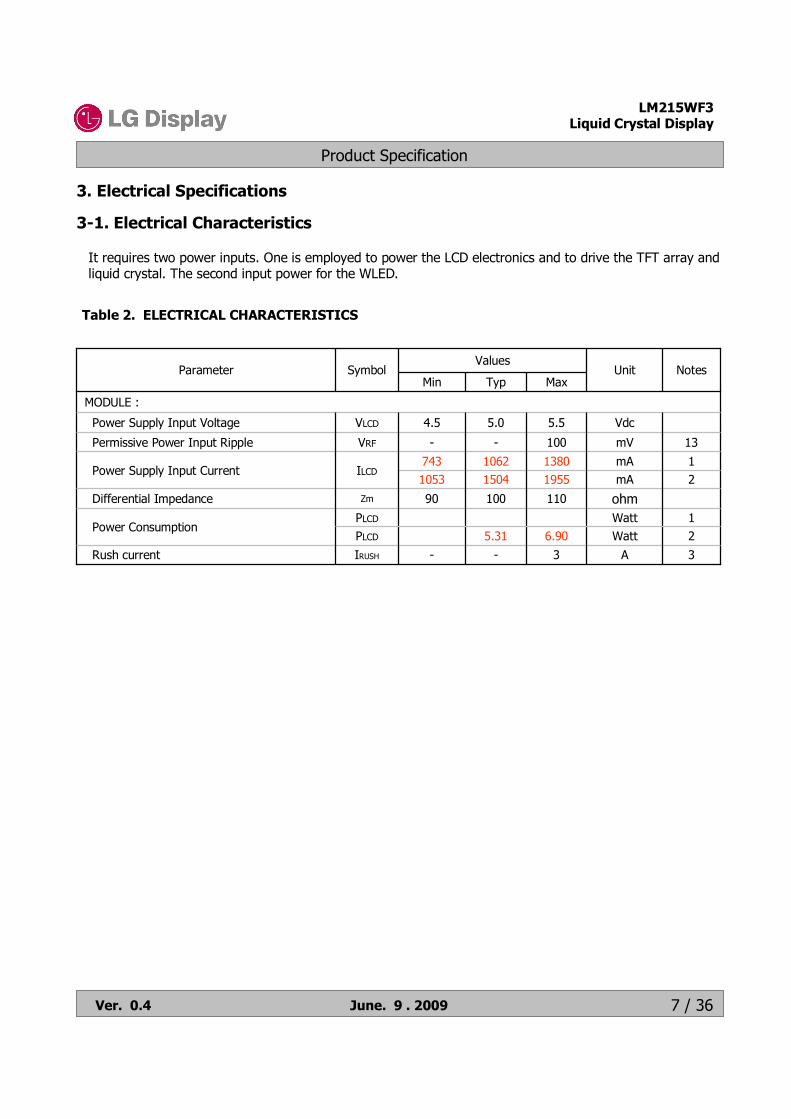
3. Electrical Specifications
3-1. Electrical Characteristics
Table 2. ELECTRICAL CHARACTERISTICS
It requires two power inputs. One is employed to power the LCD electronics and to drive the TFT array and liquid crystal. The second input power for the WLED.
1WattPLCD
3A3--IRUSHRush current
MODULE :
2Watt6.905.31PLCDPower Consumption
ohm11010090ZmDifferential Impedance
Vdc5.55.04.5VLCDPower Supply Input Voltage
13mV100--VRFPermissive Power Input Ripple
1mA138010627432mA195515041053
ILCDPower Supply Input Current
Parameter SymbolMaxTypMin
NotesUnitValues

Product Specification
8 / 36
LM215WF3Liquid Crystal Display
Ver. 0.4 June. 9 . 2009
Note.1. The specified current and power consumption are under the VLCD=5.0V, 25 2°C,fV=60Hz condition
whereas mosaic pattern(8 x 6) is displayed and fV is the frame frequency.2. The current is specified at the maximum current pattern.3. The duration of rush current is about 2ms and rising time of power Input is 1ms(min.)
White : 255GrayBlack : 0Gray Maximum current pattern
Mosaic Pattern(8 x 6) White Pattern
Product Specification
9 / 36
LM215WF3Liquid Crystal Display
Ver. 0.4 June. 9 . 2009
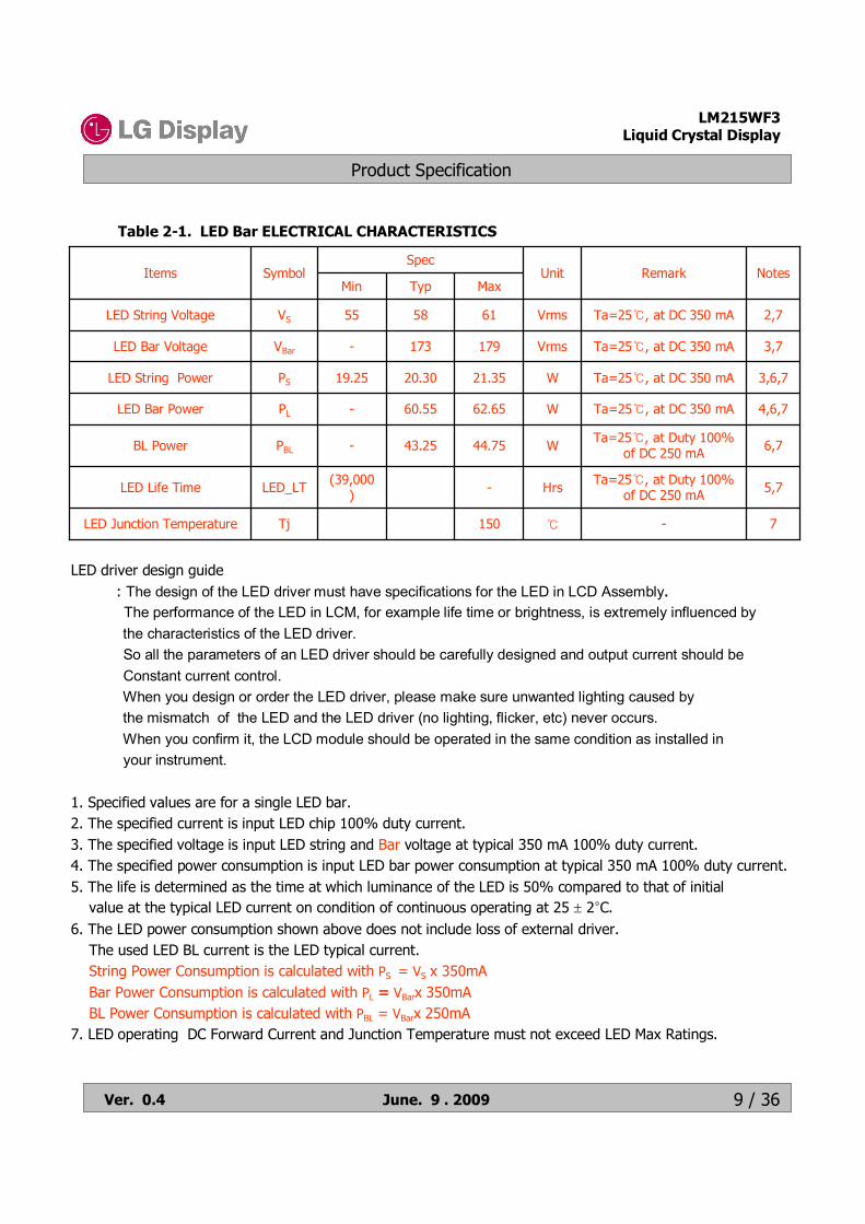
Table 2-1. LED Bar ELECTRICAL CHARACTERISTICS
LED driver design guide: The design of the LED driver must have specifications for the LED in LCD Assembly.The performance of the LED in LCM, for example life time or brightness, is extremely influenced bythe characteristics of the LED driver. So all the parameters of an LED driver should be carefully designed and output current should be Constant current control.When you design or order the LED driver, please make sure unwanted lighting caused by the mismatch of the LED and the LED driver (no lighting, flicker, etc) never occurs.When you confirm it, the LCD module should be operated in the same condition as installed in your instrument.
1. Specified values are for a single LED bar.2. The specified current is input LED chip 100% duty current.3. The specified voltage is input LED string and Bar voltage at typical 350 mA 100% duty current.4. The specified power consumption is input LED bar power consumption at typical 350 mA 100% duty current. 5. The life is determined as the time at which luminance of the LED is 50% compared to that of initial
value at the typical LED current on condition of continuous operating at 25 2°C.6. The LED power consumption shown above does not include loss of external driver.
The used LED BL current is the LED typical current. String Power Consumption is calculated with PS = VS x 350mABar Power Consumption is calculated with PL = VBarx 350mABL Power Consumption is calculated with PBL = VBarx 250mA
7. LED operating DC Forward Current and Junction Temperature must not exceed LED Max Ratings.
7-℃150TjLED Junction Temperature
5,7Ta=25℃, at Duty 100% of DC 250 mAHrs-(39,000
)LED_LTLED Life Time
6,7
4,6,7
3,6,7
3,7
2,7
Notes
Ta=25℃, at Duty 100% of DC 250 mA
Ta=25℃, at DC 350 mA
Ta=25℃, at DC 350 mA
Ta=25℃, at DC 350 mA
Ta=25℃, at DC 350 mA
Remark
W21.3520.3019.25PSLED String Power
Vrms615855VSLED String Voltage
W62.6560.55-PLLED Bar Power
MaxTypMin
Vrms179173-VBarLED Bar Voltage
W44.7543.25-PBLBL Power
UnitSpec
SymbolItems
Product Specification
10 / 36
LM215WF3Liquid Crystal Display
Ver. 0.4 June. 9 . 2009
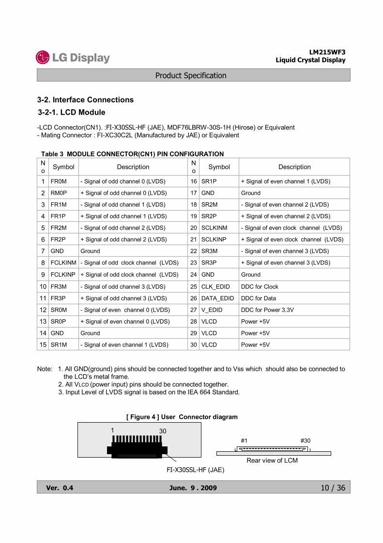
3-2. Interface Connections
Table 3 MODULE CONNECTOR(CN1) PIN CONFIGURATION
-LCD Connector(CN1). :FI-X30SSL-HF (JAE), MDF76LBRW-30S-1H (Hirose) or Equivalent- Mating Connector : FI-XC30C2L (Manufactured by JAE) or Equivalent
3-2-1. LCD Module
Note: 1. All GND(ground) pins should be connected together and to Vss which should also be connected to the LCD’s metal frame.
2. All VLCD (power input) pins should be connected together.3. Input Level of LVDS signal is based on the IEA 664 Standard.
VLCD
VLCD
VLCD
V_EDID
DATA_EDID
CLK_EDID
GND
SR3P
SR3M
SCLKINP
SCLKINM
SR2P
SR2M
GND
SR1P
Symbol
30
29
28
27
26
25
24
23
22
21
20
19
18
17
16
No
Power +5V
Power +5V
Power +5V
DDC for Power 3.3V
DDC for Data
DDC for Clock
Ground
+ Signal of even channel 3 (LVDS)
- Signal of even channel 3 (LVDS)
+ Signal of even clock channel (LVDS)
- Signal of even clock channel (LVDS)
+ Signal of even channel 2 (LVDS)
- Signal of even channel 2 (LVDS)
Ground
+ Signal of even channel 1 (LVDS)
Description
- Signal of even channel 1 (LVDS)
Ground
+ Signal of even channel 0 (LVDS)
- Signal of even channel 0 (LVDS)
+ Signal of odd channel 3 (LVDS)
- Signal of odd channel 3 (LVDS)
+ Signal of odd clock channel (LVDS)
- Signal of odd clock channel (LVDS)
Ground
+ Signal of odd channel 2 (LVDS)
- Signal of odd channel 2 (LVDS)
+ Signal of odd channel 1 (LVDS)
- Signal of odd channel 1 (LVDS)
+ Signal of odd channel 0 (LVDS)
- Signal of odd channel 0 (LVDS)
Description
SR1M15
GND14
SR0P13
SR0M12
FR3P11
FR3M10
FCLKINP9
FCLKINM8
GND7
FR2P6
FR2M5
FR1P4
FR1M3
RM0P2
FR0M1
SymbolNo
301
FI-X30SSL-HF (JAE)
#1 #30
Rear view of LCM
[ Figure 4 ] User Connector diagram

Product Specification
11 / 36
LM215WF3Liquid Crystal Display
Ver. 0.4 June. 9 . 2009
LVDS Input characteristics
NotesUnitMaxMinSymbolDescription
85MHz > Fclk ≥ 65MHzps+ 400- 400tSKEWLVDS Clock to Data Skew Margin
-
65MHz > Fclk ≥ 25MHz
- 1/7
- 600
Tclk+ 1/7tSKEW_EOLVDS Clock to Clock Skew Margin (Even to Odd)
ps+ 600tSKEW
-V2.10.3VINLVDS Input Voltage Range
-V1.80.6VCMLVDS Common mode Voltage
-mV600100|VID|LVDS Differential Voltage
NotesUnitMaxMinSymbolDescription
1. DC Specification
2. AC Specification
LVDS Even Data
LVDS Odd Clock
LVDS Even Clock
t SKEW_ EO
T clk
T clk

Product Specification
12 / 36
LM215WF3Liquid Crystal Display
Ver. 0.4 June. 9 . 2009
< Clock skew margin between channel >
< LVDS Data Format >
3. Data Format1) LVDS 2 Port
Product Specification
13 / 36
LM215WF3Liquid Crystal Display
Ver. 0.4 June. 9 . 2009
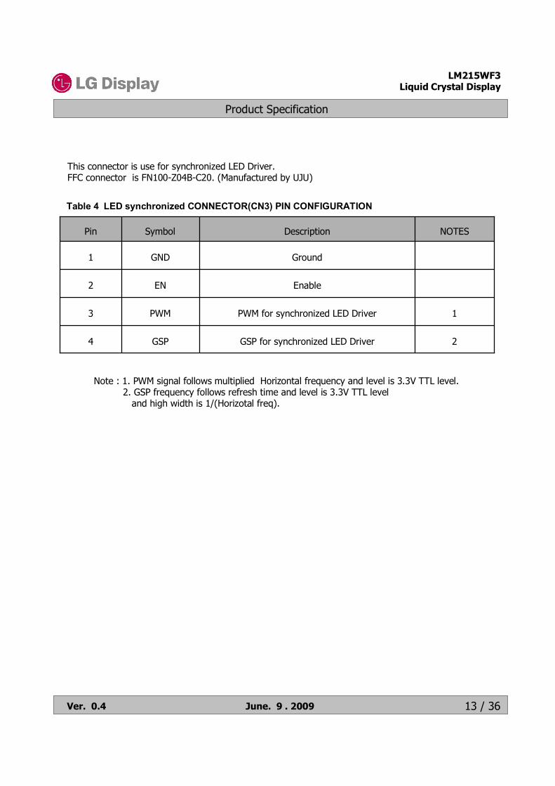
This connector is use for synchronized LED Driver. FFC connector is FN100-Z04B-C20. (Manufactured by UJU)
Enable EN2
GroundGND1
2
1
NOTES
GSP for synchronized LED Driver
PWM for synchronized LED Driver
Description
GSP
PWM
Symbol
4
3
Pin
Note : 1. PWM signal follows multiplied Horizontal frequency and level is 3.3V TTL level.2. GSP frequency follows refresh time and level is 3.3V TTL level
and high width is 1/(Horizotal freq).
Table 4 LED synchronized CONNECTOR(CN3) PIN CONFIGURATION

Product Specification
14 / 36
LM215WF3Liquid Crystal Display
Ver. 0.4 June. 9 . 2009
3-2-2. Backlight Interface
LED channel 1 Anode – Right barLED1+4
LED channel 3 cathode – Left barLED3-3
LED channel 2 Anode – Left barLED2+2
LED channel 1 cathode – Left barLED1-1
NOTES
LED channel 3 Anode – Right bar
LED channel 2 cathode – Right bar
Description
LED3+
LED2-
Symbol
6
5
Pin
Table 5 LED DRIVER CONNECTOR PIN CONFIGURATION
Driver connector: H401K-D06N-12B (Manufactured by E&T)Mating Connector: 4530K-F06N-01R (Manufactured by E&T)
123123123 ………….………………………………………………..…123
3+/ 2-/ 1+/ 3-/ 2+ /1-
16
To left sideTo right side

Product Specification
15 / 36
LM215WF3Liquid Crystal Display
Ver. 0.4 June. 9 . 2009
3-3. Signal Timing SpecificationsThis is the signal timing required at the input of the User connector. All of the interface signal timing should be satisfied with the following specifications for it’s proper operation.
Table 6. Timing Table
tHP-31-Blanking
tCLK-80-Blanking
tHP-1080-tWVvalid
Hz-60-fVFrequency
tHP-1111-tVPtotal
Vertical
tCLK/2-960-tWHvalid
KHz-66.59-fHFrequency
tCLK-1040-tHPtotal
Horizontal
MHz-69.25--Frequency
ns-14.44-tCLKPeriodDCLK
NoteUnitMaxTypMinSymbolITEM
Note:1. DE Only mode operation. The input of Hsync & Vsync signal does not
have an effect on LCD normal operation.2. The performance of the electro-optical characteristics may be influenced by variance of the
vertical refresh rates.3. Horizontal period should be even.
Product Specification
16 / 36
LM215WF3Liquid Crystal Display
Ver. 0.4 June. 9 . 2009
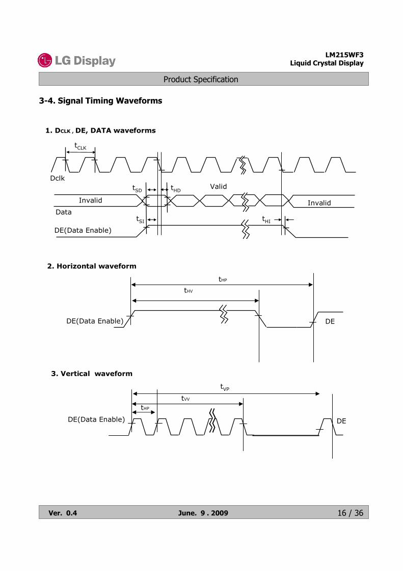
3-4. Signal Timing Waveforms
Dclk
tCLK
Valid
InvalidInvalid
DE(Data Enable)
DatatSI tHI
tSD tHD
DE(Data Enable)
tVV
tVP
DE
DE(Data Enable)
tHP
tHV
DE
1. DCLK , DE, DATA waveforms
2. Horizontal waveform
3. Vertical waveform
tHP
Product Specification
17 / 36
LM215WF3Liquid Crystal Display
Ver. 0.4 June. 9 . 2009
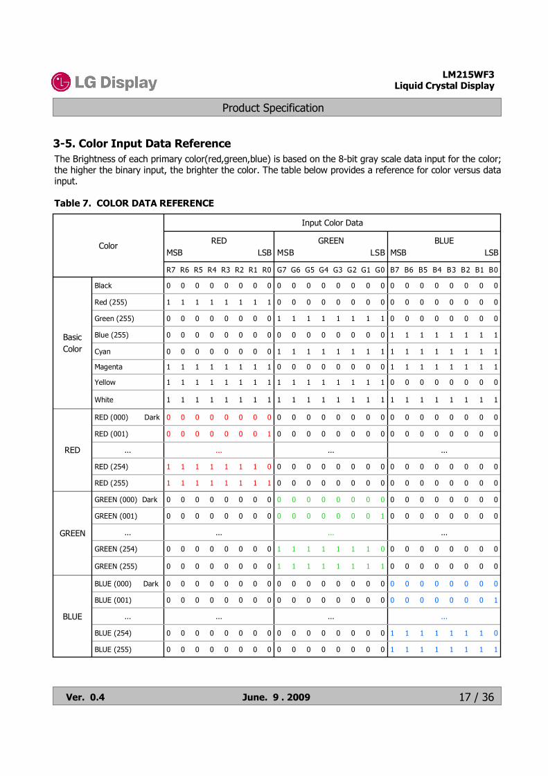
3-5. Color Input Data Reference
Table 7. COLOR DATA REFERENCE
The Brightness of each primary color(red,green,blue) is based on the 8-bit gray scale data input for the color;the higher the binary input, the brighter the color. The table below provides a reference for color versus data input.
0 0 0 0 0 0 0 00 0 0 0 0 0 0 00 0 0 0 0 0 0 0GREEN (000) Dark
GREEN
0 0 0 0 0 0 0 00 0 0 0 0 0 0 10 0 0 0 0 0 0 0GREEN (001)
............
0 0 0 0 0 0 0 01 1 1 1 1 1 1 00 0 0 0 0 0 0 0GREEN (254)
0 0 0 0 0 0 0 01 1 1 1 1 1 1 10 0 0 0 0 0 0 0GREEN (255)
0 0 0 0 0 0 0 00 0 0 0 0 0 0 00 0 0 0 0 0 0 0RED (000) Dark
RED
0 0 0 0 0 0 0 00 0 0 0 0 0 0 00 0 0 0 0 0 0 1RED (001)
............
0 0 0 0 0 0 0 00 0 0 0 0 0 0 01 1 1 1 1 1 1 0RED (254)
0 0 0 0 0 0 0 00 0 0 0 0 0 0 01 1 1 1 1 1 1 1RED (255)
0 0 0 0 0 0 0 10 0 0 0 0 0 0 00 0 0 0 0 0 0 0BLUE (001)
............
1 1 1 1 1 1 1 00 0 0 0 0 0 0 00 0 0 0 0 0 0 0BLUE (254)
1 1 1 1 1 1 1 10 0 0 0 0 0 0 00 0 0 0 0 0 0 0BLUE (255)
BLUE (000) Dark
White
Yellow
Magenta
Cyan
Blue (255)
Green (255)
Red (255)
Black 0 0 0 0 0 0 0 00 0 0 0 0 0 0 00 0 0 0 0 0 0 0
BasicColor
0 0 0 0 0 0 0 00 0 0 0 0 0 0 01 1 1 1 1 1 1 1
0 0 0 0 0 0 0 01 1 1 1 1 1 1 10 0 0 0 0 0 0 0
1 1 1 1 1 1 1 10 0 0 0 0 0 0 00 0 0 0 0 0 0 0
1 1 1 1 1 1 1 11 1 1 1 1 1 1 10 0 0 0 0 0 0 0
1 1 1 1 1 1 1 10 0 0 0 0 0 0 01 1 1 1 1 1 1 1
0 0 0 0 0 0 0 01 1 1 1 1 1 1 11 1 1 1 1 1 1 1
1 1 1 1 1 1 1 11 1 1 1 1 1 1 11 1 1 1 1 1 1 1
BLUEMSB LSB
GREENMSB LSB
REDMSB LSB
B7 B6 B5 B4 B3 B2 B1 B0G7 G6 G5 G4 G3 G2 G1 G0R7 R6 R5 R4 R3 R2 R1 R0
0 0 0 0 0 0 0 00 0 0 0 0 0 0 00 0 0 0 0 0 0 0
BLUE
Color
Input Color Data

Product Specification
18 / 36
LM215WF3Liquid Crystal Display
Ver. 0.4 June. 9 . 2009
3-6. Power Sequence
Notes : 1. Please avoid floating state of interface signal at invalid period.2. When the interface signal is invalid, be sure to pull down the power supply for LCD VLCDto 0V.3. Backlight power must be turn on after power supply for LCD and interface signal are valid.
ms---T6
s-1T7
ms50-0.01T2
ms
ms--500T3
--200T4
ms50-0.01T5
ms10-0.5T1
MaxTypMinUnits
ValuesParameter
Table 8. POWER SEQUENCE
Interface Signal, Vi(Digital RGB signal, SCDT ,Vsync, Hsync, DE, Clock to PanelLink Transmitter)
Power Supply for Backlight
Power Supply, VLCD
90%VLCD 90%
10% 10%T1
0V
Backlight ONBacklight OFF
T3
0V
T6
Backlight OFF
T4
T2 T5 T7
Valid Data
[ Figure 6 ] Power sequence

Product Specification
19 / 36
LM215WF3Liquid Crystal Display
Ver. 0.4 June. 9 . 2009
3-7. VLCD Power Dip Condition
1) Dip condition
3.5V ≤VLCD< 4.5V , td≤20ms
2) VLCD< 3.5V
VLCD-dip conditions should also follow the Power On/Off conditions for supply voltage.
4.5V
3.5V
VLCD
td
[ Figure 7 ] Power dip condition

Product Specification
20 / 36
LM215WF3Liquid Crystal Display
Ver. 0.4 June. 9 . 2009
Optical characteristics are determined after the unit has been ‘ON’ for approximately 120 minutesin a dark environment at 25±2°C. The values specified are at an approximate distance 50cm from the LCDsurface at a viewing angle of and equal to 0 ° and aperture 1 degree.FIG. 8 presents additional information concerning the measurement equipment and method.
Table 9. OPTICAL CHARACTERISTICS (Ta=25 °C, VLCD=5.0V, fV=60Hz Dclk=138.5MHz)
4. Optical Specifications
50cm
Optical Stage(x,y) LCD Module Pritchard 880 or equivalent
[ Figure 8 ] Optical characteristic measurement equipment and method
4.1ms126.5-TrRRise TimeResponse Time
4.1ms127.5-TrDDecay Time
-178-CST_VVertical5Degree
-178-CST_HHorizontalColor Shift
-178GMA_VVerticalEffective 7Degree
-178GMA_HHorizontal
82.2Gray Scale
Vertical
Horizontal
-178170V6Degree
-178170HGeneral
Viewing Angle (CR>10)
WHITE
BLUE
GREEN
RED
0.615Gy
0.306Gx
0.055By
0.145Bx
0.329Wy0.313Wx
0.333Ry
Typ +0.03
0.651
Typ-0.03
Rx
Color Coordinates [CIE1931]
3%30 WHITELuminance Variation2cd/m2-330260LWHSurface Luminance, white1
NotesUnits
-1000700CRContrast RatioMaxTypMin
ValuesSymbolParameter

Product Specification
21 / 36
LM215WF3Liquid Crystal Display
Ver. 0.4 June. 9 . 2009
Notes 1. Contrast Ratio(CR) is defined mathematically as :
It is measured at center point(Location P1)
2. Surface luminance(LWH)is luminance value at 5 points average across the LCD surface 50cm from the surface with all pixels displaying white. For more information see FIG 9. LWH = = Average[ Lon1,Lon2,Lon3,Lon4,Lon5]
3. The variation in surface luminance , WHITE is defined as :
Where L1 to L13 are the luminance with all pixels displaying white at 13 locations. For more information see FIG 9.
4. Response time is the time required for the display to transition from black to white (Rise Time, TrR) and from white to black (Decay Time, TrD). For additional information see FIG 10
5. Color shift is the angle at which the color difference is lower than 0.04.For more information see FIG 11.- Color difference (Δu’v’)
u’1, v’1 : u’v’ value at viewing angle directionu’2, v’2 : u’v’ value at front (θ=0)
- Pattern size : 25% Box size- Viewing angle direction of color shift : Horizontal, Vertical
6. Viewing angle is the angle at which the contrast ratio is greater than 10. The angles aredetermined for the horizontal or x axis and the vertical or y axis with respect to the z axis whichis normal to the LCD surface. For more information see FIG 12.
7. Effective viewing angle is the angle at which the gamma shift of gray scale is lower than 0.3.For more information see FIG 13 and FIG 14.
8. Gray scale specificationGamma Value is approximately 2.2. For more information see Table 10.
31224'
yxxu
31229'
yxyv
221
221 )''()''('' vvuuvu
pixels black all with Luminance Surfacepixels white all with Luminance Surface
RatioContrast
(%)100)L .... ,L ,(L Average
)L .. ,L,Minimum(L- )L .. ,L,Maximum(L
on5on2on1
on13on2on1on13on2on1
WHITE

Product Specification
22 / 36
LM215WF3Liquid Crystal Display
Ver. 0.4 June. 9 . 2009
The response time is defined as the following figure and shall be measured by switching the input signal for “black” and “white”.
[ FIG 10 ] Response Time
Measuring point for surface luminance & measuring point for luminance variation.
[ FIG 9 ] Measure Point for Luminance
H
1
32
54
A
B
V
Active AreaA : H/4 mmB : V/4 mm@ H,V : Active Area
H/16
V/10
6 7 8
11 12 13
9 10
whiteblack
TrR TrD
10090
100
Optical Response
black

Product Specification
23 / 36
LM215WF3Liquid Crystal Display
Ver. 0.4 June. 9 . 2009
25% Box size
2263110155206240B
2263110155206240G
2263110155206240R
blackNeutral 3.5Neutral 5Neutral 6.5Neutral 8White
172151363765145B
126622122714832G
352072411977226R
cyanMagentaYellowRedGreenBlue
2958868717424B
162193396769104G
2301607621156219R
Orange yellowYellow greenPurpleModerate redPurplish blueOrange
1781854616112345B
19911810211214256G
114129778520698R
Bluish greenBlue flowerFoliageBlue skyLight skinDark skin
Average RGB values in Bruce RGB for Macbeth Chart
FIG. 11 Test Pattern
Color shift is defined as the following test pattern and color.

Product Specification
24 / 36
LM215WF3Liquid Crystal Display
Ver. 0.4 June. 9 . 2009
[ FIG 12 ] Viewing angle
Dimension of viewing angle range.
Normal Y E
= 0, Right
= 180, Left
= 270, Down
= 90, Up
br LaVL )log()log()log( aVrLL b
Here the Parameter α and γ relate the signal level V to the luminance L.The GAMMA we calculate from the log-log representation (FIG. 14)
[ FIG 13 ] Sample Luminance vs. gray scale (using a 256 bit gray scale)
[ FIG 14 ] Sample Log-log plot of luminance vs. gray scale

Product Specification
25 / 36
LM215WF3Liquid Crystal Display
Ver. 0.4 June. 9 . 2009
Table 10. Gray Scale Specification
0.100
100
74.5
53.1
35.5
21.7
11.5
4.71
1.08
255
223
191
159
127
95
63
31
Relative Luminance [%] (Typ.)Gray Level
Product Specification
26 / 36
LM215WF3Liquid Crystal Display
Ver. 0.4 June. 9 . 2009
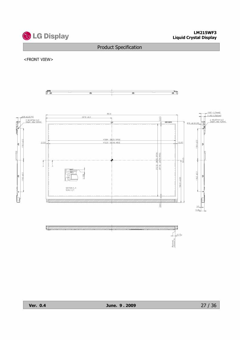
5. Mechanical Characteristics
The contents provide general mechanical characteristics. In addition the figures in the next page are detailed mechanical drawing of the LCD.
267.3mmVertical
Hard coating(2H)Glare, Low Reflection treatment of the front polarizerSurface Treatment
TBDWeight
272.32mmVertical
305.25mmVertical
15.8mmDepth
475.2mmHorizontalActive Display Area
479.84mmHorizontalBezel Area
495.6mmHorizontal
Outline Dimension
Notes : Please refer to a mechanic drawing in terms of tolerance at the next page.
Product Specification
27 / 36
LM215WF3Liquid Crystal Display
Ver. 0.4 June. 9 . 2009
<FRONT VIEW>

Product Specification
28 / 36
LM215WF3Liquid Crystal Display
Ver. 0.4 June. 9 . 2009
<REAR VIEW>

Product Specification
29 / 36
LM215WF3Liquid Crystal Display
Ver. 0.4 June. 9 . 2009
6. Reliability
Environment test condition
Ta= 40 °C ,90%RHHumidity condition Operation7
0 - 40,000 feet(12192m)Altitude
storage / shipment8
Shock level : 100GWaveform : half sine wave, 2msDirection :±X, ±Y, ±Z
One time each direction
Shock test(non-operating)6
Wave form : randomVibration level : 1.0G RMSBandwidth : 10-300HzDuration : X,Y,Z, 10 min
One time each direction
Vibration test(non-operating)5
Ta= 0°C 240hLow temperature operation test4
Ta= 50°C 50%RH 240hHigh temperature operation test3
Ta= -20°C 240hLow temperature storage test2
Ta= 60°C 240hHigh temperature storage test1
ConditionTest ItemNo
Product Specification
30 / 36
LM215WF3Liquid Crystal Display
Ver. 0.4 June. 9 . 2009
7. International Standards
7-1. Safety
7-2. EMC
a) ANSI C63.4 “Methods of Measurement of Radio-Noise Emissions from Low-Voltage Electrical and Electrical Equipment in the Range of 9kHZ to 40GHz. “American National Standards Institute(ANSI),1992
b) C.I.S.P.R “Limits and Methods of Measurement of Radio Interface Characteristics of InformationTechnology Equipment.“ International Special Committee on Radio Interference.
c) EN 55022 “Limits and Methods of Measurement of Radio Interface Characteristics of InformationTechnology Equipment.“ European Committee for Electrotechnical Standardization.(CENELEC), 1998( Including A1: 2000 )
a) UL 60950-1:2003, First Edition, Underwriters Laboratories, Inc.,Standard for Safety of Information Technology Equipment.
b) CAN/CSA C22.2, No. 60950-1-03 1st Ed. April 1, 2003, Canadian Standards Association,Standard for Safety of Information Technology Equipment.
c) EN 60950-1:2001, First Edition, European Committee for Electrotechnical Standardization(CENELEC)European Standard for Safety of Information Technology Equipment.
d) IEC 60950-1:2001, First Edition, The International Electrotechnical Commission (IEC)Standard for Safety of Information Technology Equipment.(Including report of IEC60825-1 Ed. 1.22001, clause 8 and clause 9)

Product Specification
31 / 36
LM215WF3Liquid Crystal Display
Ver. 0.4 June. 9 . 2009
8. Packing
8-1. Designation of Lot Mark
a) Lot Mark
A B C D E F G H I J K L M
A,B,C : SIZE(INCH) D : YEAR E : MONTH F ~ M : SERIAL NO.
Note1. YEAR
2. MONTH
Mark
Year
0
2010
6
2006
7
2007
8
2008
9
2009
4
2004
5
2005
321
200320022001
B
Nov
Mark
Month
A
Oct
6
Jun
7
Jul
8
Aug
9
Sep
4
Apr
5
May
C321
DecMarFebJan
b) Location of Lot Mark
Serial No. is printed on the label. The label is attached to the backside of the LCD module.This is subject to change without prior notice.
a) Package quantity in one box : TBD
b) Box Size : TBD
8-2. Packing Form

Product Specification
32 / 36
LM215WF3Liquid Crystal Display
Ver. 0.4 June. 9 . 2009
9. PRECAUTIONS
Please pay attention to the followings when you use this TFT LCD module.
9-1. MOUNTING PRECAUTIONS
(1) You must mount a module using holes arranged in four corners or four sides.(2) You should consider the mounting structure so that uneven force (ex. Twisted stress) is not applied to the
module. And the case on which a module is mounted should have sufficient strength so that external force is not transmitted directly to the module.
(3) Please attach the surface transparent protective plate to the surface in order to protect the polarizer.Transparent protective plate should have sufficient strength in order to the resist external force.
(4) You should adopt radiation structure to satisfy the temperature specification.(5) Acetic acid type and chlorine type materials for the cover case are not desirable because the former
generates corrosive gas of attacking the polarizer at high temperature and the latter causes circuit break by electro-chemical reaction.
(6) Do not touch, push or rub the exposed polarizers with glass, tweezers or anything harder than HBpencil lead. And please do not rub with dust clothes with chemical treatment.Do not touch the surface of polarizer for bare hand or greasy cloth.(Some cosmetics are detrimentalto the polarizer.)
(7) When the surface becomes dusty, please wipe gently with absorbent cotton or other soft materials like chamois soaks with petroleum benzene. Normal-hexane is recommended for cleaning the adhesives used to attach front / rear polarizers. Do not use acetone, toluene and alcohol because they cause chemical damage to the polarizer.
(8) Wipe off saliva or water drops as soon as possible. Their long time contact with polarizer causes deformations and color fading.
(9) Do not open the case because inside circuits do not have sufficient strength.
9-2. OPERATING PRECAUTIONS
(1) The spike noise causes the mis-operation of circuits. It should be lower than following voltage : V=±200mV(Over and under shoot voltage)
(2) Response time depends on the temperature.(In lower temperature, it becomes longer.)(3) Brightness depends on the temperature. (In higher temperature, it becomes lower.)
And in lower temperature, response time(required time that brightness is stable after turned on) becomeslonger.
(4) Be careful for condensation at sudden temperature change. Condensation makes damage to polarizer or electrical contacted parts. And after fading condensation, smear or spot will occur.
(5) When fixed patterns are displayed for a long time, remnant image is likely to occur.(6) Module has high frequency circuits. Sufficient suppression to the electromagnetic interference shall be
done by system manufacturers. Grounding and shielding methods may be important to minimized theinterference.
(7) Please do not give any mechanical and/or acoustical impact to LCM. Otherwise, LCM can’t be operated its full characteristics perfectly.
(8) A screw which is fastened up the steels should be a machine screw. (if not, it causes metallic foreign material and deal LCM a fatal blow)
(9) Please do not set LCD on its edge.
Product Specification
33 / 36
LM215WF3Liquid Crystal Display
Ver. 0.4 June. 9 . 2009
Since a module is composed of electronic circuits, it is not strong to electrostatic discharge. Make certain that treatment persons are connected to ground through wrist band etc. And don’t touch interface pin directly.
9-3. ELECTROSTATIC DISCHARGE CONTROL
Strong light exposure causes degradation of polarizer and color filter.
9-4. PRECAUTIONS FOR STRONG LIGHT EXPOSURE
When storing modules as spares for a long time, the following precautions are necessary.
(1) Store them in a dark place. Do not expose the module to sunlight or fluorescent light. Keep the temperature between 5°C and 35°C at normal humidity.
(2) The polarizer surface should not come in contact with any other object.It is recommended that they be stored in the container in which they were shipped.
9-5. STORAGE
9-6. HANDLING PRECAUTIONS FOR PROTECTION FILM
(1) The protection film is attached to the bezel with a small masking tape.When the protection film is peeled off, static electricity is generated between the film and polarizer.This should be peeled off slowly and carefully by people who are electrically grounded and with well ion-blown equipment or in such a condition, etc.
(2) When the module with protection film attached is stored for a long time, sometimes there remains a very small amount of glue still on the bezel after the protection film is peeled off.
(3) You can remove the glue easily. When the glue remains on the bezel surface or its vestige is recognized, please wipe them off with absorbent cotton waste or other soft material like chamois soaked with normal-hexane.