k5 5 optical processes in semiconductors:...
TRANSCRIPT

K5
______________________________________________________________________________________________________________________________
Electronics Laboratory: Optoelectronics and Optical Communications 22.03.2010
5-1
5 Optical Processes in Semiconductors: 22/03/2010 Optisch induzierte Polarisation Eines Moleküls Polarized Atomic Dipole in Optical Field Blue Silicon Carbide Light Emitting Diode LED Representation of band-to-band transitions in Semiconductors

K5
______________________________________________________________________________________________________________________________
Electronics Laboratory: Optoelectronics and Optical Communications 22.03.2010
5-2
Goals of the chapter:
Design of optical SC-devices (Laser, Photodetectors, optical amplifiers, etc.) depends critically on the calculation of the carrier transition rates R, the rate-equations of carriers and photons and the optical gain g(ω,n)
• Nonclassical description of the motion of bound electrons in the static force fields of the atomic nucleus or crystal lattice and a oscillating light wave
• The equation of motion and polarization has to be described in a quantized 2-energy level material system by a quantum mechanical model based on the perturbed time dependent Schrödinger-equation
• The description of the interaction between light field and a 2-energy band Semiconductor needs an extension of the discrete 2-level concepts to continuum-to-continuum, resp. band-to-band optical transitions
Methods for the Solution:
• The classical model for electron motion r(t) of “electrons-on-springs” will be replaced by the time-dependent Schrödinger-equation (TSE) for a harmonic oscillator providing a statistical expectation value ⟨r(t)⟩
• The quantum mechanical equation of motion of the expectation value ⟨r(t)⟩ of bound or quasi-free charges in atoms and SC will be obtained for weak optical fields.
• Perturbation-theory leads to the Transition-Rates R and a realistic microscopic susceptibilities χ(ω,n2,n1) depending on the of charge carriers densities n1, n2 in the lower and upper levels
• The quantum-mechanical analysis shows for carrier inversion n2>n1 optical gain g(ωopt) occurs

K5
______________________________________________________________________________________________________________________________
Electronics Laboratory: Optoelectronics and Optical Communications 22.03.2010
5-3
5 Optical Processes in Semiconductors:
Introduction:
The classical dipole oscillator model „electrons on springs“ breaks down for a) the quantized energy exchange between atom and light field, b) the microscopic force constant and the relation to carrier state occupancy, that is:
the „spring force constant“ kDP and the damping γ D of the dipole motion are not physically defined
Realization of a positive χ’’>0, resp. γ<0 to obtain optical gain is not obvious? Carrier motion in a atomic system with discrete quantized energy levels E2 and E1 and Distribution of carriers n2, n1 occupying these levels influence the optical gain g ?
Separation of transparent and absorbing spectral regions of SC
Goal: Semi-classical QM-Theory of the atomic oscillator and a light field with
- a classical optical field and
- a quantum mechanical (QM) description of the microscopic, induced dipole motion by an optical field

K5
______________________________________________________________________________________________________________________________
Electronics Laboratory: Optoelectronics and Optical Communications 22.03.2010
5-4
Step 1: Einstein-Theory of optical transitions
• Phenomenological semi-classical description of optical processes in a quantized 2-level medium by the so called Einstein-Rate-equation formalism of optical transitions (Einstein 1905)
Step 2: Quantum mechanical model of optical transitions • Quantum mechanical model for the dipole-oscillator (perturbation theory) (~1930)
Relation between microscopic material parameters and the quantum mechanical susceptibility χ Condition for optical gain in atoms and SC and the concept of “pumping” and carrier inversion Extension of the 2-level-interaction to band-to-band transitions in SCs calculation of optical gain / absorption spectrum g(ω,n) in SC as a function of carrier density n, p.
K5
______________________________________________________________________________________________________________________________
Electronics Laboratory: Optoelectronics and Optical Communications 22.03.2010
5-5
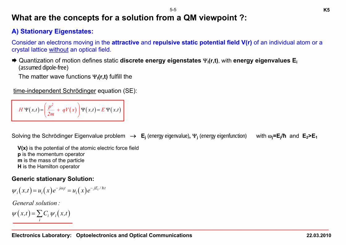
What are the concepts for a solution from a QM viewpoint ?: A) Stationary Eigenstates:
Consider an electrons moving in the attractive and repulsive static potential field V(r) of an individual atom or a crystal lattice without an optical field.
Quantization of motion defines static discrete energy eigenstates ΨI(r,t), with energy eigenvalues Ei (assumed dipole-free)
The matter wave functions ΨI(r,t) fulfill the time-independent Schrödinger equation (SE):
( ) ( ) ( ) ( )2pH qV xx,t x,t x,m
tE2
⎛ ⎞+⎜ ⎟
⎝Ψ = Ψ
⎠Ψ =
Solving the Schrödinger Eigenvalue problem → Ej (energy eigenvalue), Ψj (energy eigenfunction) with ωj=Ej/ħ and E2>E1 V(x) is the potential of the atomic electric force field p is the momentum operator m is the mass of the particle H is the Hamilton operator Generic stationary Solution:
( ) ( ) ( )
( ) ( )
i ij t jE / ti i i
i ii
x,t u x e u x e
General solution :x,t C x,t
ωψ
ψ ψ
− −= =
= ∑

K5
______________________________________________________________________________________________________________________________
Electronics Laboratory: Optoelectronics and Optical Communications 22.03.2010
5-6
with the normalizations:
i i
2i
i
*i i
i i
1
C 1
C
C
ψ ψ ψ ψ
ψ ψ
ψ ψ
= = →
=
=
=
∑
Interpretation of the Ci:
The coefficient 2 *i i iC C C= i is proportional to the probability of finding the system in the state ( )i x,tψ with the energy
Ei. B) Time dependence Eigenstate occupation
Perturbation of the static potential field V(r) by a superposed harmonic optical field (E, H, ω) with its dynamic potential Vopt(r,t)
Definition: weak perturbation the optical field is much weaker than the static atomic field, Vatom >>Vopt
QM-interaction between N quantized 2-level system (E2,E1) (level E2 with N2 electrons, level E1 with N1 electrons) and a
classical, non-quantized optical harmonic EM-field (E, H) of spectral energy-density W(ω), ( )2
EMEW
Volω
ω∂
=∂ ∂
The interaction changes of the occupation probabilities (N2(t)/N , N1(t)/N) of the 2-level system by photon absorption or emission, resp. transitions between levels combined
with an energy exchange due to the EM-forces of the light field

K5
______________________________________________________________________________________________________________________________
Electronics Laboratory: Optoelectronics and Optical Communications 22.03.2010
5-7
Quantum mechanical perturbation analysis: time-dependent SE
( ) ( ) ( ) ( ) ( )2
2 optatom qV x,tpH x,t q x,t i x,tm t
V x⎛ ⎞ ∂
Ψ = + + Ψ = Ψ⎜ ⎟ ∂⎝ ⎠
static potential oscillating potential of the EM-field (ωopt)
Assumed dynamic solution ( )x,tΨ :
a superposition of static solutions ( ) ( )1 2x,t ; x,tΨ Ψ with time-dependent coefficients Ci(t)
( ) ( ) ( ) ( ) ( ) ( ) ( ) ( ) ( )1 21 1 2 2 1 1 2 2
j t j tx,t C t x,t C t x,t C t u x e C t u x eω ω− −Ψ = Ψ + Ψ = +
C1(t), C2(t) are now time-functions
( )x,tΨ describes the quantized system completely in its interaction with the optical field !
Calculation of the time dependent expectation values of the variables of the atomic system relevant for optical properties:
( ) ( ) ( ) ( ) ( )2 1x t ; P t ; ; N t ; N t etc.χ ω
E1
E2
Materie
EM-Feldklassisch
EM-field: E0,ω
ψ2 ψ1
up- / down transitions
K5
______________________________________________________________________________________________________________________________
Electronics Laboratory: Optoelectronics and Optical Communications 22.03.2010
5-8
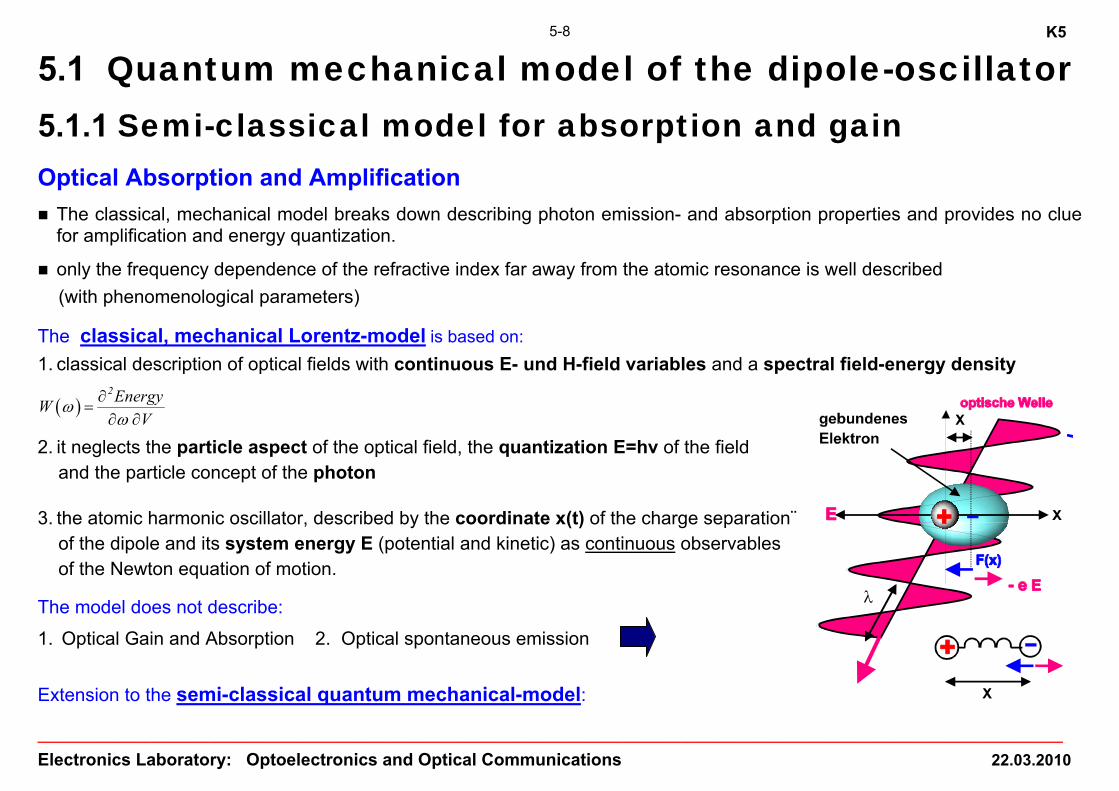
5.1 Quantum mechanical model of the dipole-oscillator
5.1.1 Semi-classical model for absorption and gain
Optical Absorption and Amplification
The classical, mechanical model breaks down describing photon emission- and absorption properties and provides no clue for amplification and energy quantization.
only the frequency dependence of the refractive index far away from the atomic resonance is well described
(with phenomenological parameters) The classical, mechanical Lorentz-model is based on:
1. classical description of optical fields with continuous E- und H-field variables and a spectral field-energy density
( )2EnergyW
Vω
ω∂
=∂ ∂
2. it neglects the particle aspect of the optical field, the quantization E=hv of the field and the particle concept of the photon
3. the atomic harmonic oscillator, described by the coordinate x(t) of the charge separation¨ of the dipole and its system energy E (potential and kinetic) as continuous observables of the Newton equation of motion. The model does not describe:
1. Optical Gain and Absorption 2. Optical spontaneous emission Extension to the semi-classical quantum mechanical-model:

K5
______________________________________________________________________________________________________________________________
Electronics Laboratory: Optoelectronics and Optical Communications 22.03.2010
5-9
5.1.2 Interaction of a EM-field with a discrete 2-level system
Introduction: (Lit. Loudon)
The optical field is represented by a classical, not quantized field H(r,t), E(r,t) → description by Maxwell’s equations
The medium response and its microscopic electrodynamics with respect to energy quantization E1, E2 under interaction with the optical field E(t) (QM-description of the equation of motion for the electron position x(t))
→ description of expectation value of <x(t)> of the QM-dipole by the time-dependent Schrödinger equation
Atomic 2-level systems (E1, E2 , N1, N2) which interact with an optical EM-field (ω, E, H) exchange energy resulting in a change of the occupation probability of the of the electrons, resp. in a change of the electron numbers N1, N2.
The goal is to calculate the time evolution of N1(t) and N2(t) for an idealized “2-level atom” and the formation of an atomic dipole p(t) under the influence of the harmonic optical field ( ) ( )E r,t , H r,t .
Strong interaction only close to the atomic transition frequency ( )21 2 1E E /ω = − Quantum mechanical 2-Level-System as a model: (quantitative description, QM >1930)
1-electron-atom-model with (no collision processes → infinite state-lifetime) 2 discrete „sharp“ energy-levels E1 and E2 (E1<E2)
The 2 energy levels are Eigenvalues E1 und E2 of the 1-D time independent Schrödinger-equation for the electron in the stationary, parabolic potential V(x) of the nucleus:
Energy-Levels of a harmonic Oscillator (electron in a parabolic potential V(x)= -kx2 , no light field)
( )3 3x , EΨ (3. excited state)
( )2 2 2x ,N ,EΨ 2.excited state
( )1 1 1x , N ,EΨ 1.ground state E1
E2
Transition 2↔1
x
-eV(x) Energy E

K5
______________________________________________________________________________________________________________________________
Electronics Laboratory: Optoelectronics and Optical Communications 22.03.2010
5-10
Stationary state without optical field: Time independent Schrödinger-Equation
The matter wave Ψ(x,t) representing the probabilistic motion of a particle of constant total Energy E=Etot (kinetic and potential) in a stationary electrostatic potential V(x) is a solution (eigenfunction) with the energy eigenvalue E of:
( ) ( ) ( ) ( ) ( ) ( )2
, , , ,2kin potpH x t H H x t qV x x t E x tm
⎛ ⎞Ψ = + Ψ = + Ψ = Ψ⎜ ⎟
⎝ ⎠ H=Hamilton (Energy)-Operator
Stationary Schrödinger equation with time-invariant potential V(x)
( ) ( )( )
( )
2
22 2
2
amilton Operator of the time-independent potential V x of the positive nucleus
mpulse operator ;
E total energy potential and kinetic energy
V x time-independent potential of
pH qV x H2m
p j i px x
−
= =
=
⎛ ⎞= + =⎜ ⎟
⎝ ⎠∂ ∂
= − = = −∂ ∂
( )
the nucleus
q charge of the particle (-e)x,t Eigenfunction of the matter wave
=
=ψ
( ) ( ) ( )( )
( ) ( ) ( ) ( ) ( )
j t jE / t
2
i i i i i i
with the time-space-dependent Eigenfunctions x,t u x e u x e ,
resp. spatial term u x and Energy Eigenvalues E as solutions :
pH u x qV x u x E u x, with u x spatial Eigenfunction and Eigenvalue E2m
− −= =
⎛ ⎞= + = =⎜ ⎟
⎝ ⎠
ωψ

K5
______________________________________________________________________________________________________________________________
Electronics Laboratory: Optoelectronics and Optical Communications 22.03.2010
5-11
( )*
i j i j ij ii ij
Eigenfunction are a complete orthogonal and normalized :
u u u u dx with : 1 , 0 if i j
μ
δ δ δ+∞
−∞
= = = = ≠∫
iorthonormal set =
(without proof)
( ) ( )( ) ( )
1
2
jE / t1 1 1 1 1
jE / t2 2 2 2 2
E : x,t u x e Standing wave with the oscillation frequency ω =E /
E : x,t u x e Standing wave with the oscillation frequency E /ω
−
−
Ψ =
Ψ = =
General solution: ( ) ( ) ( )1 1 2 2 1 2
2 2 2 21 1 1 2 1 1
, , , , constant
C C are the probabilities of finding the system at E or E ; C C 1
x t C x t C x t C C
and
ψ ψ ψ= + =
+ =
Ψ(x,t) describes the statistical behaviour of the electron in the potential field V(x) with constant total Energy E.
ΨΨ*=IΨI2 is interpreted as probability density of finding the electron at the position x, if normalized to: * 1dxψψ =∫ .
the statistical expectation value <x> for the space variable x of the particle is (probability of finding the particle at x) :
( ) ( ) ( ) ( )BRA KETDefinition
of BRA KETnotation
x x,t x x,t dx u x x u x dx u x u+∞ +∞
∗ ∗
−∞ −∞−
= Ψ Ψ = =∫ ∫
we will use x to describe the dipole
p e x etc.χ= − →
the stationary solutions Ψ(x,t) are, in order to be stationary (E=const.), non-radiating, resp. free of a dipole moment.
K5
______________________________________________________________________________________________________________________________
Electronics Laboratory: Optoelectronics and Optical Communications 22.03.2010
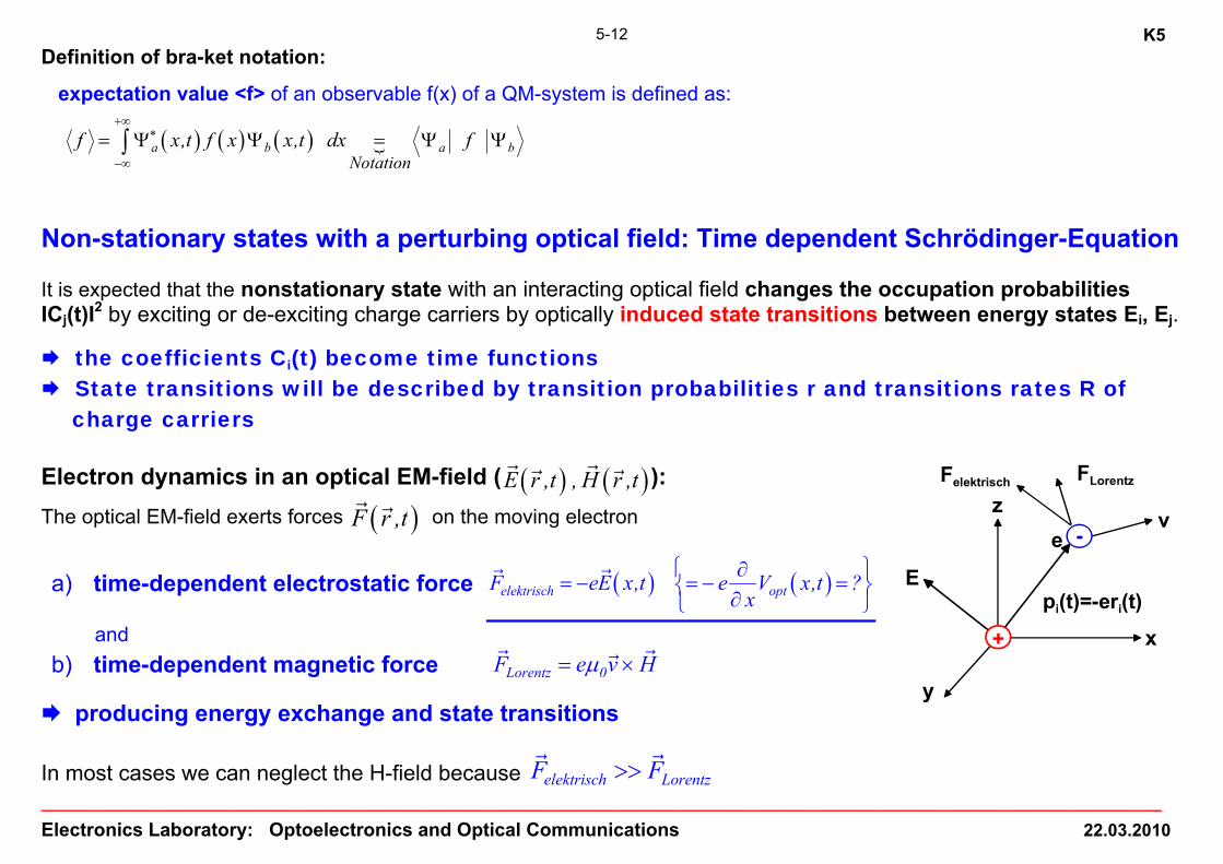
5-12Definition of bra-ket notation:
expectation value <f> of an observable f(x) of a QM-system is defined as:
( ) ( ) ( )a b a bNotation
f x,t f x x,t dx f+∞
∗
−∞
= Ψ Ψ = Ψ Ψ∫
Non-stationary states with a perturbing optical field: Time dependent Schrödinger-Equation It is expected that the nonstationary state with an interacting optical field changes the occupation probabilities ICj(t)I2 by exciting or de-exciting charge carriers by optically induced state transitions between energy states Ei, Ej.
the coefficients Ci(t) become time functions State transitions will be described by transition probabilities r and transitions rates R of charge carriers
Electron dynamics in an optical EM-field ( ( ) ( )E r ,t , H r ,t ): The optical EM-field exerts forces ( )F r ,t on the moving electron
a) time-dependent electrostatic force ( ) ( )elektrisch optF eE x,t e V x,t ?x
⎧ ⎫∂= − = − =⎨ ⎬∂⎩ ⎭
and b) time-dependent magnetic force Lorentz 0F e v Hμ= ×
producing energy exchange and state transitions
In most cases we can neglect the H-field because elektrisch LorentzF F>>
x
y
ze -
+
Epi(t)=-eri(t)
v
Felektrisch FLorentz

K5
______________________________________________________________________________________________________________________________
Electronics Laboratory: Optoelectronics and Optical Communications 22.03.2010
5-13
Schematic representation of basic interactions of a 2-level system and an optical field:
Photon Absorption Spontaneous Photon-Emission Stimulated Photon-Emission
4
(Electron-Hole-Pair Generation) (Electron-Hole-Pair Annihilation) Photon-Annihilation Photon-Generation
e-transition from: E1 → E2 E2 → E1 E2 → E1
EM-Radiation field changes occupation probabilities by level-transitions
e ee
h h h
Exciting photon Stimulated Photon
In
hv=E2-E1 in out
out
excited state ground state
Ene
rgy
E

K5
______________________________________________________________________________________________________________________________
Electronics Laboratory: Optoelectronics and Optical Communications 22.03.2010
5-14
What are the transition rates R and how do they depend on the optical field ?
In historical order:
1) Einstein Theory: (A. Einstein, 1905 without QM)
The 2-level system exchanges energy with the EM-field of frequency ω only if the photon energy E=ħω=E2-E1 (resonance)
1) electrons in the ground state E1 absorb a photon and make an up-ward transition to the excited (upper) state E2.
2) electrons in the excited state E2 make a down-ward transition to the ground state E1 emitting an incoherent spontaneous photon or emit a coherent stimulated photon, if a stimulating field is present.
3) Stimulated absorption and emission are proportional to the energy density of the optical field, the probabilities of
the occupation of the initial state and the final state being empty.
Definition: Transition-Pair (E2, E1) = initial and final state:
The initial and final state (E2 and E1) of an atom form a local transition pair. In isolated atoms the occupation of a level means that the other level is necessarily empty and available for a transition. Details see p.5-16.
2) Quantum Mechanics: (after ~1930)
The motion of the bound electron in an optical field (where the energy E of the 2-level system is not constant) is described by the matter wave Ψ(x,t) of the electron in the time dependent potential V(x,t) = V(x) + Vopt(t).
The time-dependent EM-forces induce a microscopic dipole extracting (attenuation) or transferring (amplification) energy from or to the field depending on the relative phase.
the energy-exchange excites electron transition from the ground to the excited state and vice versa if the optical frequency ωopt is close to the transition frequency ω21.
K5
______________________________________________________________________________________________________________________________
Electronics Laboratory: Optoelectronics and Optical Communications 22.03.2010
5-15
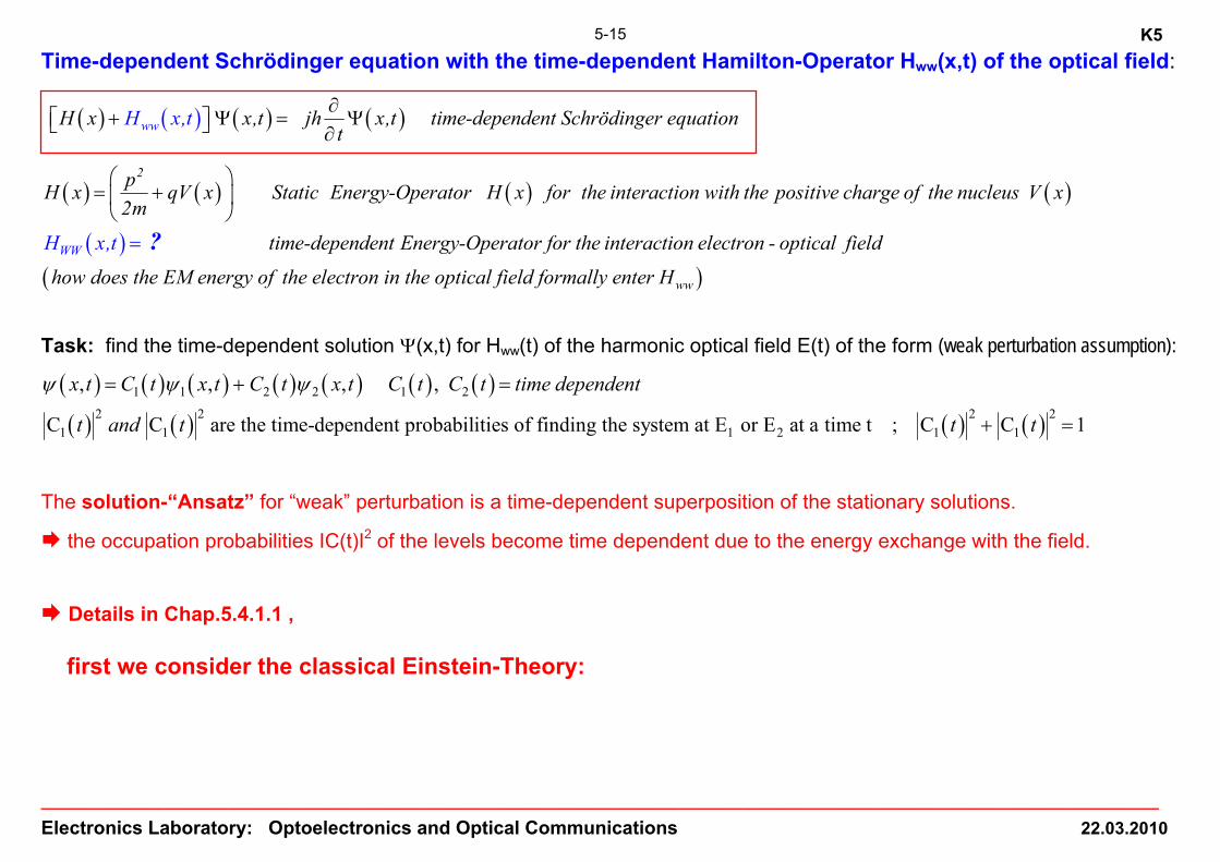
Time-dependent Schrödinger equation with the time-dependent Hamilton-Operator Hww(x,t) of the optical field:
( ) ( ) ( ) ( )
( ) ( ) ( ) ( )
( )
w
2
w
WW
H x x,t jh x,t time-dependent Schrödinger equationt
pH x qV x Static Energy-Operator H x for the interaction with the positive charge
H x,t
H x,t
of the nucleus V x2m
time-dependent Energy-Operator for the in=
∂+ Ψ = Ψ⎡ ⎤⎣ ⎦ ∂
⎛ ⎞= +⎜ ⎟
⎝ ⎠?
( )ww
teraction electron - optical field
how does the EM energy of the electron in the optical field formally enter H
Task: find the time-dependent solution Ψ(x,t) for Hww(t) of the harmonic optical field E(t) of the form (weak perturbation assumption):
( ) ( ) ( ) ( ) ( ) ( ) ( )( ) ( ) ( ) ( )
1 1 2 2 1 2
2 2 2 21 1 1 2 1 1
, , , ,
C C are the time-dependent probabilities of finding the system at E or E at a time t ; C C 1
x t C t x t C t x t C t C t time dependent
t and t t t
ψ ψ ψ= + =
+ =
The solution-“Ansatz” for “weak” perturbation is a time-dependent superposition of the stationary solutions.
the occupation probabilities IC(t)I2 of the levels become time dependent due to the energy exchange with the field.
Details in Chap.5.4.1.1 , first we consider the classical Einstein-Theory:

K5
______________________________________________________________________________________________________________________________
Electronics Laboratory: Optoelectronics and Optical Communications 22.03.2010
5-16
5.1.3 Einstein-Theory of the optical transition in 2-level systems (see lit: Loudon)
Concept: Phenomenological theory of A. Einstein (1905).
Light fields and matter interact by EM-field induced stimulated and spontaneous level-transitions in 2-level atomic systems by photon emission and absorption at the transition frequency.
The transition modify the occupation probabilities pi of the energy levels Ei in the atomic system (rate equations).
1) Transition Postulate:
Matter is built from quantized 2-level systems (transition pairs) representing atoms undergoing interaction with a classical optical wave.
Interaction with the EM-field induces “upward or downward” transition between the levels (absorption, emission).
The ↑- or ↓-transitions between levels i and j are described by changes occupation probability ICi(t)I2 and ICj(t)I2:
a) Definition : Transition Probability rij (i → j) change of level occupation probability pj per unit time in a single 2-level system
2
ij j jr p / t C / t i int ial state ; j final state= ∂ ∂ = ∂ ∂ = =
b) Transition Rates Rij (i→j) change of the particle density Nj in state Ej per unit time and volume of a collection of atomic density N
22ij j ij i ij iR N / t V r N r N C= ∂ ∂ ∂ = =

K5
______________________________________________________________________________________________________________________________
Electronics Laboratory: Optoelectronics and Optical Communications 22.03.2010
5-17Describing the occupation probability of state i of the transition as
( ) ( ) 2i ip t C t=
we get for the 2-level system E2 and E1 with
( ) ( ) ( ) ( )2 2 2 22 1 2 1C t and C t fulfilling C t C t 1+ =
( ) ( )2 2
j iij
C t C tr
t t∂ ∂
= = −∂ ∂
i= initial state, j= final state
and obtain for the transition rate of Ni identical pairs
( ) ( )2 2
j iij i i
C t C tR N N
t t∂ ∂
= = −∂ ∂
Ni=density of transition pairs i→j, resp. atoms
2) Spontaneous emission Postulate:
For thermodynamic reasons or due to the additional quantization of the optical field (zero-point energy) spontaneous emission transitions (downward transitions) are possible without an exciting optical field.
Spontaneous emission is spatially isotropic.
3) Stimulated emission Postulate:
The stimulated emitted photon induced by an external field has the same frequency ω, phase φ and propagation direction (wave number) k as the stimulating photon.
The two photons are indistinguishable.
Stimulated emission results in a coherent amplification of the EM-field.

K5
______________________________________________________________________________________________________________________________
Electronics Laboratory: Optoelectronics and Optical Communications 22.03.2010
5-18
5.1.3.1 Transition rates Rij between discrete energy levels in atoms
Goal:
We want to relate the “up” and “down” transition rate R12, R21 and R21,spont to the properties of the spectral energy density W(ω), resp. W(E) or photon density sph of the optical field and the densities of the available transition pairs N1 (level E1 for up-ward transitions) and N2 (level E2 for up-ward transitions).
Ni is the occupation density of level Ei. Definition: spectral energy density W(ω) (SED)
Optical broad-band fields E(r,t), H(r,t) are characterized in the frequency domain by their cycle averaged spectral energy density W(ω)
( ) ( ) ( ) ( )2 2E EW ; W E with the relation :
V E VW W Eω
ωωω ∂ ∂
= = =∂ ∂ ∂
=∂
(SED)
For a monochromatic, harmonic optical fields (as an ideal case): ( ) ( ) { } ( )opt opt optj t j t j t0 0E t E cos t Re e E / 2 e eω ω ωω + + −= = = +
the SED W(ω) becomes a δ-function (1-sided spectrum):
( ) ( ) ( )2
0 0opt ph opt
1 EW ED s2 2
εω δ ω ω ωδ ω ω= = − = − E0 ⇔ sph
using the concept of the photon as a energy quantum E=ħωopt and the photon density sph At Einstein’s time lasers producing quasi-ideal monochromatic fields (cos-field) did not exist. Only optical broadband (thermal) sources characterized by W(ω) were available. So it was natural to formulate the dependence of the transition probability rij related to W(ω).
W(ω)
ω ω0
Δω
K5
______________________________________________________________________________________________________________________________
Electronics Laboratory: Optoelectronics and Optical Communications 22.03.2010
5-19
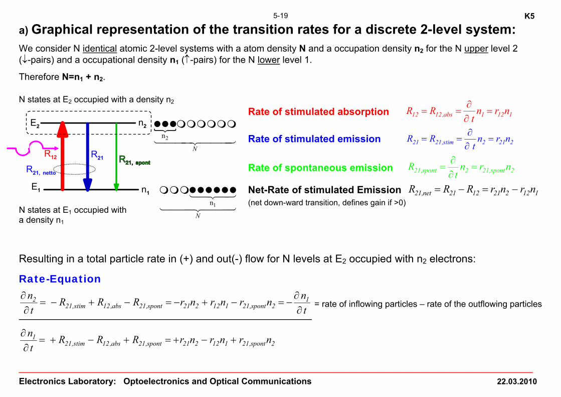
a) Graphical representation of the transition rates for a discrete 2-level system:
We consider N identical atomic 2-level systems with a atom density N and a occupation density n2 for the N upper level 2 (↓-pairs) and a occupational density n1 (↑-pairs) for the N lower level 1.
Therefore N=n1 + n2.
N states at E2 occupied with a density n2
N states at E1 occupied with a density n1
Resulting in a total particle rate in (+) and out(-) flow for N levels at E2 occupied with n2 electrons:
Rate-Equation
2 121,stim 12,abs 21,spont 21 2 12 1 21,spont 2
n nR R R r n r n r nt t
∂ ∂= − + − = − + − = −
∂ ∂ = rate of inflowing particles – rate of the outflowing particles
121,stim 12,abs 21,spont 21 2 12 1 21,spont 2
n R R R r n r n r nt
∂= + − + = + − +
∂
Rate of stimulated absorption 12 12,abs 1 12 1R R n r nt
∂= = =
∂
Rate of stimulated emission 21 21,stim 2 21 2R R n r nt
∂= = =
∂
Rate of spontaneous emission 21,spont 2 21,spont 2R n r nt
∂= =
∂
Net-Rate of stimulated Emission 21,net 21 12 21 2 12 1R R R r n r n= − = − (net down-ward transition, defines gain if >0)
n2
n1E1
E2
R12 R21
R21, netto
2n
N
1n
N
K5
______________________________________________________________________________________________________________________________
Electronics Laboratory: Optoelectronics and Optical Communications 22.03.2010
5-20
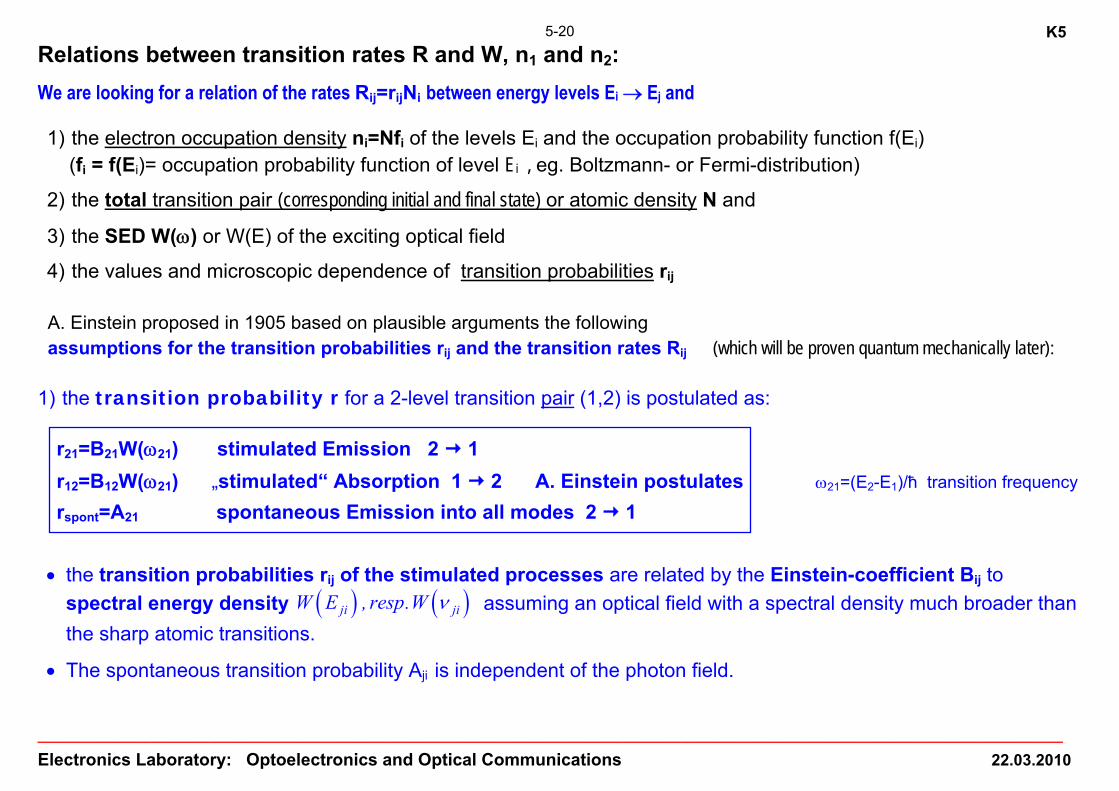
Relations between transition rates R and W, n1 and n2:
We are looking for a relation of the rates Rij=rijNi between energy levels Ei → Ej and
1) the electron occupation density ni=Nfi of the levels Ei and the occupation probability function f(Ei) (fi = f(Ei)= occupation probability function of level Ei , eg. Boltzmann- or Fermi-distribution)
2) the total transition pair (corresponding initial and final state) or atomic density N and
3) the SED W(ω) or W(E) of the exciting optical field
4) the values and microscopic dependence of transition probabilities rij A. Einstein proposed in 1905 based on plausible arguments the following assumptions for the transition probabilities rij and the transition rates Rij (which will be proven quantum mechanically later):
1) the transition probability r for a 2-level transition pair (1,2) is postulated as:
r21=B21W(ω21) stimulated Emission 2 1 r12=B12W(ω21) „stimulated“ Absorption 1 2 A. Einstein postulates ω21=(E2-E1)/ħ transition frequency
rspont=A21 spontaneous Emission into all modes 2 1 • the transition probabilities rij of the stimulated processes are related by the Einstein-coefficient Bij to
spectral energy density ( ) ( )ji jiW E , resp.W ν assuming an optical field with a spectral density much broader than the sharp atomic transitions.
• The spontaneous transition probability Aji is independent of the photon field.
K5
______________________________________________________________________________________________________________________________
Electronics Laboratory: Optoelectronics and Optical Communications 22.03.2010
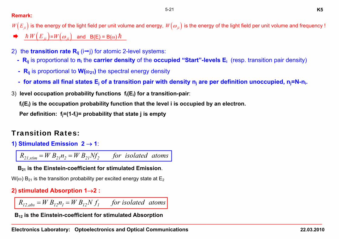
5-21Remark:
( )jiW E is the energy of the light field per unit volume and energy, ( )jiW ω is the energy of the light field per unit volume and frequency !
( )jiW E = ( )jiW ω and B(E) = B(ω)
2) the transition rate Rij (i j) for atomic 2-level systems:
- Rij is proportional to ni the carrier density of the occupied “Start”-levels Ei (resp. transition pair density)
- Rij is proportional to W(ω21) the spectral energy density
- for atoms all final states Ej of a transition pair with density nj are per definition unoccupied, nj=N-ni. 3) level occupation probability functions fi(Ei) for a transition-pair:
fi(Ei) is the occupation probability function that the level i is occupied by an electron.
Per definition: fj=(1-fi)= probability that state j is empty
Transition Rates:
1) Stimulated Emission 2 → 1:
21,stim 21 2 21 2R W B n W B Nf for isolated atoms= =
B21 is the Einstein-coefficient for stimulated Emission.
W(ω) B21 is the transition probability per excited energy state at E2 2) stimulated Absorption 1→2 :
12,abs 12 1 12 1R W B n W B N f for isolated atoms= =
B12 is the Einstein-coefficient for stimulated Absorption

K5
______________________________________________________________________________________________________________________________
Electronics Laboratory: Optoelectronics and Optical Communications 22.03.2010
5-22
3) spontaneous Emission 2→1 per mode:
21,spont 21 2 21 2R A n A N f for isolated atoms= =
A21 is the Einstein-coefficient for spontaneous Emission
4) net stimulated Rate R21,netto 2 → 1:
( )21,net 21,stim 12,abs 21,net 21 2 12 1 21 2 12 1R R R R W B n B n WB Nf WB Nf for isolated atoms= − = = − = −
n1 = density of the transition pairs with the electron in the ground state E1 (Valence band) n2 = density of the transition pairs with the electron in the excited state E2 ( Conduction band) N = density of all atomic transition pairs, resp. density of the atoms f1 = occupation probability for an electron in the ground state E1 (eg. Boltzmann or Fermi-Function) f2 = occupation probability for an electron in the excited state E2 (eg. Boltzmann orFermi-Function)
Condition for optical amplification and population inversion:
The net-rate of stimulated emission (difference between stimulated Emission und Absorption) must be R21,net >0, in order that the photon density in the optical field is increased optical gain g is possible.
For B12=B21 the occupation probability of the upper energy level 2 must be larger than the lower level 1:
POPULATION INVERSION n2 =Nf2> n1=Nf1 , → f2(E2)>f1(E1) Important Remark:
In thermal equilibrium with the thermal blackbody radiation at a finite temperature T the electrons are distributed according to a Boltzmann-Distribution with n2<<n1. This means that no gain is possible in thermally excited materials.
Electrons have to be “pumped” or transferred actively to the upper level to create population inversion by non-equilibrium
K5
______________________________________________________________________________________________________________________________
Electronics Laboratory: Optoelectronics and Optical Communications 22.03.2010
5-23
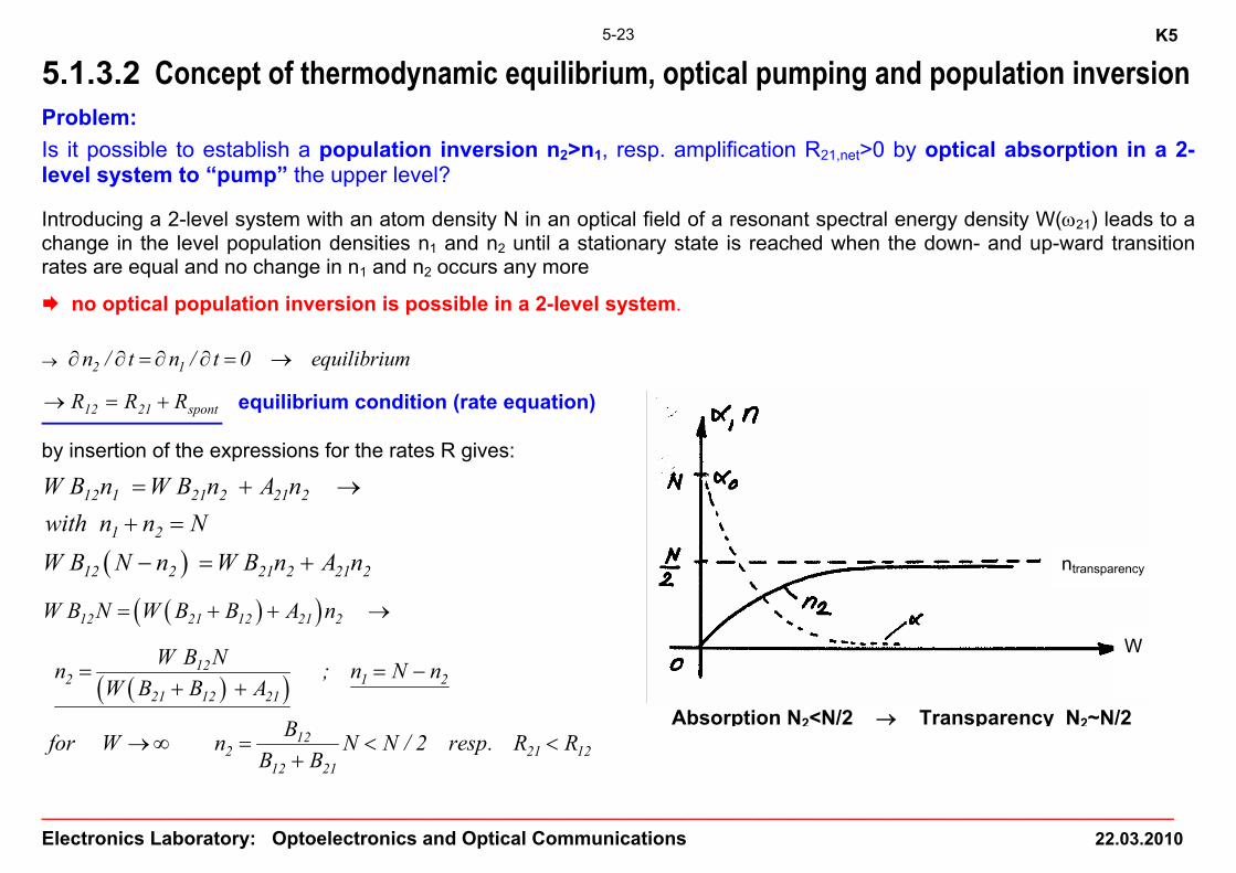
5.1.3.2 Concept of thermodynamic equilibrium, optical pumping and population inversion
Problem:
Is it possible to establish a population inversion n2>n1, resp. amplification R21,net>0 by optical absorption in a 2-level system to “pump” the upper level? Introducing a 2-level system with an atom density N in an optical field of a resonant spectral energy density W(ω21) leads to a change in the level population densities n1 and n2 until a stationary state is reached when the down- and up-ward transition rates are equal and no change in n1 and n2 occurs any more
no optical population inversion is possible in a 2-level system.
→ 2 1n / t n / t 0 equilibrium∂ ∂ = ∂ ∂ = →
spont2112 RRR +=→ equilibrium condition (rate equation)
by insertion of the expressions for the rates R gives:
( )
12 1 21 2 21 2
1 2
12 2 21 2 21 2
W B n W B n A nwith n n NW B N n W B n A n
= + →+ =
− = +
( )( )
( )( )
12 21 12 21 2
122 1 2
21 12 21
122 21 12
12 21
W B N W B B A n
W B Nn ; n N nW B B A
Bfor W n N N / 2 resp. R RB B
= + + →
= = −+ +
→ ∞ = < <+
Absorption N2<N/2 → Transparency N2~N/2
W
ntransparency

K5
______________________________________________________________________________________________________________________________
Electronics Laboratory: Optoelectronics and Optical Communications 22.03.2010
5-24The rate of absorption is always larger than the rate of stimulated emission, therefore
a simple 2-level system “optically pumped” by a light field remains always absorbing or at most becomes transparent (n2=n1).
No population inversion (n2>n1) or gain can be reached by optical pumping at the transition frequency ! The same formalism as above can be used for the
Thermal Boltzmann equilibrium with the blackbody radiation: W(ω) = ρbb(ω) (see chap.5.2.1)
In reality a 2-level system with no external light field W=0 must be in equilibrium with the always present „black body radiation“ with the spectral energy density ρbb(ω) and exhibit an electron distribution according to a Boltzmann-distribution, where n1>>n2 , resp.
( )( )2 1 2 1n / n exp E E / kT= − − The resulting relationship was used by A. Einstein to relate the constant A to B

K5
______________________________________________________________________________________________________________________________
Electronics Laboratory: Optoelectronics and Optical Communications 22.03.2010
5-25
Optical population inversion in a 3-Niveau-System:
Reaching optical amplification g>0 in a 2-level system requires: 21,stim 12,abs 21,netR R resp. R 0> > resp. 2/Nnn transp,22 >>
To enforce a population inversion, resp. inverting the population in a 2 → 1 transition (ω21) by an optical „pump“ field Wpump(ωpump) such that 2 2,transp 1n n n> > it is necessary to introduce a 3rd level for artificially injecting carriers in level E2 without removing them by stimulated emission of the pump light again.
Establishment of such a non-equilibrium (Inversion) 2 2,transpn n> is called Pumping or Inversion of the medium Optical pumping of a 3-level system:
The simplest way to achieve population inversion between level E2 and E1 is the introduction of a third, lower level E0 Assumptions:
- active optical transitions (eg. gain) occur only between 1 ↔ 2 - optical pumping take place between 0 ↔ 2 - the transition probability r10 →∞ (“empty” 1-level) - A20 should be small
ωpump=ω20=(E2-E0)/ ħ ω21=(E2-E1)/ ħ (active transition 1-2) and ω20> ω21
n1 +n2 + no=N Ideally the transition 1 → 0
occurs infinitively fast (r10 → ∞, n1=0) meaning level 1 is always empty !
2: n2 Wactive=0 1: n1 → ~0 0: n0
(B12)
A10→∞
A21
A20
B20
Pump level
B02

K5
______________________________________________________________________________________________________________________________
Electronics Laboratory: Optoelectronics and Optical Communications 22.03.2010
5-26Calculation of the equilibrium rates between the 3 levels leads to:
Lasing transition: 2-1 (without lasing W12 =0), pump transition: 0-2 (ρpump)
( ) ( )
0 1 2
pump 20 0 2 2 20 21
21 2 10 1 2 1
2
12
1010 21
1 21
0 1
pump 202
21pump 20
10
static : 0 ; n n n N density of atoms ;t
level 2 : W B n n n A A 0
level 1: A n A n 0 condition for inversion n n 0n A 1n Areplacing n and n
W B N0 n
AW BA
W 0
2
τ τ
=∂
= + + + = =∂
− − + =
− = → > →
= > → <
→
< =⎛ ⎞
+⎜ ⎟⎝ ⎠
( )1 2 21 10 2
2120 21
10
N N and n n A / A nA 22A A A
< < = <++ +
Depending on the optical and electrical properties of the gain-medium the inversion of transition 2 → 1 is realized by:
a) absorption of pump-light of a shorter wavelength than the active transition (many solid state lasers, Er-doped fiber amplifiers etc.)
b) Injection of carriers by an electrical current in forward biased pn-diodes (SC-Diode Lasers)
c) Ionization in gases (eg. HeNe-Gas Laser)

K5
______________________________________________________________________________________________________________________________
Electronics Laboratory: Optoelectronics and Optical Communications 22.03.2010
5-27
5.1.4 Stimulated Emission Rate R21,net and Optical Amplification g
Goal: • Relation between gain and optical transition rate g ↔ R21,net
Stimulated emission generates temporal and spatial coherent photons (ω, k, φ) which amplify the stimulating light field.
• Relation between the net stimulated emission rate R21 or the carrier densities difference n2-n1 and the gain constant g(R21,net) = g(n2,n1)=dI/dx/I.
• Relation between the susceptibility χ( n2-n1) for the wave-picture.
Wave representation as a photon stream: (necessary for coupling to transition rates)
The optical field is represented as coherent superposition of elementary wave packets with an energy quantum ω
In analogy to the electrical current a photon flux density (intensity) can be associated to a current of photons with the photon density sph which propagate with the group velocity vgr (particle picture of light)
Relation between photon density sph and field amplitude E=E0cos(ωt) for a harmonic TE plane wave sph ⇔ E0
( )
gr
0 0 ph 0 ph ph
1v2
0 0 0 gr ph gr 0 ph 0 r0 0
1energy density : w E E * s E 2 s / E s2
or from the int ensity I :
1 1 1I S E H E E E wv s v E 2 s / ;2 2 2
ε μ
ε ω ω ε
ε ε ω ω ε ε ε εμ εμ
=
= = → = =
= = × = = = = ⎯⎯⎯⎯→ = =
( ) ( ) ( ) ( )opt 0 0 opt opt ph opt
with the spectral energy density : (1 sided )1W w E E * s2
ω δ ω ω ε δ ω ω ω δ ω ω
−
= − = − = −

K5
______________________________________________________________________________________________________________________________
Electronics Laboratory: Optoelectronics and Optical Communications 22.03.2010
5-28
x
z
y
dx
H
E
sph
β
x+dxx
hω
dx
Graphical representation of photon-flux through a volume element:
nph = Photon density = sph E = electrical field strength H = magnetic field strength S = Pointing-vector w=energy density
vgr
Relation between the energy density w and the photon density sph of an optical field:
classical energy density of optical EM-fields
a) electric energy density DE21
b) magnetic energy density BH21
c) cycle and spatially averaged energy density photon inflow photon outflow
of an harmonic optical field 20
Ww EV 2
ε∂= =
∂
d) intensity (Pointing-Vector) photon generation / destruction 1 2 gr ph grI S / E H wv n vω= = × = =
associated photon density: 20
ph phw En s
2ε
ω ω= = =
dVol

K5
______________________________________________________________________________________________________________________________
Electronics Laboratory: Optoelectronics and Optical Communications 22.03.2010
5-29
x
z
y
dx
sph
x+dx
x
hωI I + ΔI
R21,net
Calculation of the relation g(Rstim(n2,n1)):
the net-rate of stimulated emission R21,net changes the photon density sph in transit. Depending R21,net> or <0 optical amplification g or attenuation α will result.
The optical field with photon density sph(x,t), resp. intensity I(x,t)=sph(x,t)ħωvgr travels with vgr in the x-direction through a thin layer Δx of amplifying medium in time Δt.
The medium increasing its intensity by ΔI, resp Δsph. From the definition of the attenuation α:
( ) ( ) xI 1 I x I 0 ex I
αα −∂= − → =
∂ using this definition of α: α>0 means absorption, α<0 gain !
because the intensity I=sphvgrħω is proportional sph, we write:
( ) ( ) ( ) ( )( ) ( ) ( ) ( )
ph
ph
ph ph ph ph ph
s
I sI x x I x I I x I x x
s x x s x s s x s x xΔ
+ Δ = + Δ − Δ ⎯⎯⎯→
+ Δ = + Δ − Δ
∼α
α
R21,netto sph R21,netto sph + Δsph x x + Δx Δt=Δx/vgr
Δsph
Photon inflow
Photon outflow
Photon generation / annihilation

K5
______________________________________________________________________________________________________________________________
Electronics Laboratory: Optoelectronics and Optical Communications 22.03.2010
5-30
ph 21,netto
ph
gr
ph
To travel through the layer Δx and increase its intensity by I, resp. s the wave needs the time t:
t x / v
during the time Δt the wave increases its photon de s R Δt of stimn ulated photonssity by
s R
:
Δ Δ
Δ = Δ
Δ
Δ =
=
Δ
( ) ( ) ( ) ( )
( )( )
ph
21 12 ph ph gr ph gr
21,netto ph
21,n
g
e to
r
t
s
t R R t s x x s x v t s x g v t
R / s x v g
Δ
Δ = − Δ = − Δ = − Δ = Δ
= − = −
α
α
α
Important relation ship to connect fields and rates: g ⇔ R21

K5
______________________________________________________________________________________________________________________________
Electronics Laboratory: Optoelectronics and Optical Communications 22.03.2010
5-31
5.2 Spontaneous emission in 2-Level Systems
(see lit. Coldren, Yariv) Goal:
To determine 2 relations between the 3 Einstein-coefficients A, B21, B12 we can use the thermodynamic equilibrium situation between a
2-level system and the
Blackbody-Radiation with a spectral power density W(E)=ρbb(E) (obtained from thermodynamics) and
a carrier distribution obeying the Boltzmann-distribution (see Physik II, 2.Sem.)
Finally there is still one unknown remaining, eg. B which can only be determined only from a quantum mechanical description of atomic polarization or experimentally from an absorption measurement.
5.2.1 Spontaneous Emissions-Processes
R21,spont Spontaneous-Emission-Postulate
The spontaneous transition of an excited QM-system without external optical disturbance into the lower energy-level has no classical equivalent.
This can only be understood by QM if also the optical field is quantized into a harmonic oscillator (2.quantization, zero-point fluctuations of an optical mode)
Spontaneous emission is a necessary process to explain that an optical 2-level system perturbed by an external optical field (resulting in non-equilibrium carrier densities n2+Δn2 and n1+Δn1 with Δn= carrier disturbance) can relax back to equilibrium (Bolzmann-distribution) after switching off the disturbance.
Spontaneous emission is a thermodynamic necessity to establish equilibrium

K5
______________________________________________________________________________________________________________________________
Electronics Laboratory: Optoelectronics and Optical Communications 22.03.2010
5-32
5.2.2 Thermodynamic equilibrium: quantized atomic system ↔ blackbody radiation
Following A. Einstein we consider the rate equations for the electrons of a 2level system in thermodynamic equilibrium (Boltzmann) with the known blackbody EM-radiation field with a spectral energy density ρBB(ω) inside a „2-level blackbody“ of temperature T. The carrier distribution obeys Boltzmann distribution.
Idea: In thermodynamic equilibrium the spectral energy density is BBW ρ= and the electron densities n2 and n1 obey Boltzmann-statistics. In equilibrium the transition rates between levels 2 → 1 and 1 → 2 must be equal:
( ) ( )21 BB 21,spont 12 BBR R Rρ ρ+ = ρbb = ?
Spectral mode ρmode and energy ρBB density of blackbody-radiation: (without proof, see Physik II)
We obtain the spectral energy density BBρ of blackbody radiation by counting the EM-modes inside a Volume V and multiplying the
spectral mode density ρmode with the average number of thermal photons per mode n and the photon energy E. n=refractive index.
( ) ( ) ( )BB modeE E n E Eρ ρ=
( )( )
( ) ( ) ( )
( )( )
( )
3 3 3 3ph,BB
BB BB3 3 3 3
3 3ph,BB
BB 2 3
modeE
d n1 E / n ds hv8 n E 8 n E 1d EE energy density Eexp E / kT 1 exp E / kT
no di1 d Eh c h c
ρ
d n1 E / n ds hv8 n E d Ev energy de
spersion
nsityexp E / kT 1 d vh
o
c
f n n
+= ≅ =
− −⎡ ⎤ ⎡ ⎤⎣ ⎦ ⎣ ⎦
+= =
−⎡ ⎤⎣ ⎦
π πρ ρ
πρ ( )BB vρ
E=hv= energy of blackbody radiation photons n= refractive index of blackbody T= temperature of the blackbody h= Plank constant
volume V

K5
______________________________________________________________________________________________________________________________
Electronics Laboratory: Optoelectronics and Optical Communications 22.03.2010
5-33
For the derivation of the ρBB we made use of:
Spectral blackbody mode density:
( ) ( )
( )
3 2 3 2 2mode
mod e 3 3 3 3
3 2 2mode
mod e 3
8 n E d n 8 n E d NE 1 E / n blackbody-mode densityd E d E dVolh c h c
8 n v d Nvd vdVolc
π πρ
πρ
⎡ ⎤= + ≅ =⎢ ⎥
⎣ ⎦
≅ =I
Photon-occupation ( )n E per mode in thermal equilibrium:
In thermal equilibrium each mode i carries according to the Bose-Einstein-Statistic for photons in photons.
( ) ( )i
i i i ii E kT
Bose-Einstein-Statistic:1n E 1 occupation probability of mode i with photons ofenergy E
exp E / kT 1ω
>>
= << =−⎡ ⎤⎣ ⎦
Therefore we get ( ) ( )BB mode i iE E n Eρ ρ=

K5
______________________________________________________________________________________________________________________________
Electronics Laboratory: Optoelectronics and Optical Communications 22.03.2010
5-34
5.2.3 Relation between the Einstein-coefficients A21, B21 and B12 Example: atomic 2-level transition pairs
In the thermodynamic equilibrium with the spectral energy density ρBB of the thermal radiation:
1) total emission rate = total absorption rate
BB112BB221221 nBnBnA ρρ =+ A21n2 = spont. photon emission rate into all vacuum modes with density ρbb 2) Boltzmann-equilibrium of the level occupation for n2, n1
122121
1
2 EEE;kTEexp
nn
−=⎟⎠⎞
⎜⎝⎛ −=
insertion of the ratio of n2/n1 leads to:
( )( ) ( ) ( )
mod e 2121
3 321 21 21
BB 21 mod e 21 21 213 321 21
12 21 E n
A / B 8 n E 1E E n EE exp E / kT 1h cB / B exp 1kT ρ
πρ ρ= = =−⎛ ⎞ ⎡ ⎤⎣ ⎦−⎜ ⎟
⎝ ⎠
Comparision of the coefficients on both sides of the equation results in:
Relation between Einstein-coefficients B and A
( ) ( ) ( )
21 12
3 3 3 321
mode3 3 3
for energy density for enery densityper energy E per frequency v
B B B
8 n E 8 n hvA B E B v B E Eh c c
π π ρ
= =
⎛ ⎞ ⎛ ⎞= = =⎜ ⎟ ⎜ ⎟
⎝ ⎠ ⎝ ⎠

K5
______________________________________________________________________________________________________________________________
Electronics Laboratory: Optoelectronics and Optical Communications 22.03.2010
5-35Important remark:
The relations are valid at a particular energy difference E21=E2-E1 of a particular mode. The coefficient A which is the inverse of a spontaneous carrier lifetime ( )spont iA 1/ Eτ= is the Einstein coefficient for the spontaneous emission into all modes of free space. (also not only lasing modes or resonator modes, see spont. emission factor β in chap.6)
Considering the ratio between the net stimulated rate and the spontaneous rate:
(measure for the ease to invert the material)
In thermal equilibrium ( ) ( ) ( )opt 21 bb 21 mod e 21 21 21E E E n Eρ ρ ρ= = we have the following magnitude-relation of the net stimulated and spontaneous rates:
( )21,net
2 121,spont
21,spont 21,stim 12,abs
R 1 n 1 if E hv kT and n nR exp E / kT 1
R R , R Thermal Radiation Source
= = << = > <<−
>>
kT~26meV@300K, hv~1eV → E/kT~40
Conclusion:
Systems in thermodynamic equilibrium (eg. lamps) do virtually not emit coherent, resp. stimulated radiation (Rstim << Rspont).
Only for LASERs, excited by pumping into a strong non-equilibrium state (inverted) with n2>n1 , optical gain and coherent radiation becomes possible and dominant.
Optical gain is more difficult to achieve at short wavelengths (microwave Masers have been invented before optical Lasers).
( )21,net 21 12 2 1 opt
3 3
21,spont 2 23
R R R B n n
8 n hvR An B nc
ρ
π
= − = −
⎛ ⎞= = ⎜ ⎟
⎝ ⎠

K5
______________________________________________________________________________________________________________________________
Electronics Laboratory: Optoelectronics and Optical Communications 22.03.2010
5-36
Relation between the Einstein coefficient B and the attenuation α:
A direct experimental measurement of A or B is difficult, however we will show that there is a simple relation ship between the Einstein coefficients and the attenuation α.
The attenuation α, describing the decrease of the optical beam intensity I(L)=I(0)e-αL with propagation distance L in the medium of known absorption state, is relatively easy to measure.
Assuming a weak monochromatic optical field (close to thermal equilibrium) with the spectral energy density:
( ) ( ) ( )ph 0 21,net 2 1 phW s hv R B n n sω δ ω ω ω= − → = −
We have already shown that α and R21,netto are related by: h
( ) ( ) ( ) ( ) ( ) ( )21,net ph gr ph 2 1 ph gr 2 1 grE R E / s v s hv B n n / s v hv B n n / vα = − = − − = − −
Using a weak optical beam for attenuation measurements, which does not disturb the equilibrium Boltzmann population:
2 21 2 1 2 1 21
1 1 1
1n ~N
n E n n n n Eexp expn kT n N kT
⎡ ⎤− −⎛ ⎞ ⎛ ⎞= − → ≅ = − −⎜ ⎟ ⎜ ⎟⎢ ⎥⎝ ⎠ ⎝ ⎠⎣ ⎦
with known N=atoms / unite volume
( ) ( ) ( ) ( )gr gr2 1
212 1
v v1 1B E E E ; E E hvEhv n n hv N exp 1kT
α α= − = − − =− ⎡ ⎤⎛ ⎞− −⎜ ⎟⎢ ⎥⎝ ⎠⎣ ⎦
From the measurement of α with known atom density N and group velocity vgr we obtain B and also A.

K5
______________________________________________________________________________________________________________________________
Electronics Laboratory: Optoelectronics and Optical Communications 22.03.2010
5-37
Conclusions:
• The Einstein model postulates 1) the energy quantization of the medium and 2) transition rates between the states
• The Einstein coefficients B12, B21 and A21 have been introduced formally as postulates and can not be related directly to the material properties (eg. electronic potentials, eff. mass) on a microscopic level
• The model allows the description of optical gain g by population inversion • The spontaneous emission is a quantum-mechanical phenomenon and has no classical equivalent. However it is a thermodynamic necessity for the classical system to relax to thermal equilibrium. • The model is also capable of representing the black-body radiation, resp. the relation between A and B

K5
______________________________________________________________________________________________________________________________
Electronics Laboratory: Optoelectronics and Optical Communications 22.03.2010
5-38
5.3 Pumping and Population Inversion Optical amplification α<0 or g>0 requires a population inversion → R21,net>0 → n2>n1.
A population inversion can not be realized in thermodynamic equilibrium (eg. heating T→∞).
Non-equilibrium is enforced by an influx of carriers into the higher energy level E2 PUMPING (pumping transitions in 3- or multi-level systems).
5.3.1 Optical and electrical pumping
Inverted transition pairs are realized by Absorption of „pump-light“ (optical pumping) in the isolating crystal matrix containing the active atoms. The atoms must provide at least an additional 3rd energy level E3 (3-level-system), at λpump<λ21. For so called solid-state lasers based on active metal atoms like Nd, Er, Cr, etc. embedded in an isolating crystal matrix of eg. Erbium in Glass, Cr in Ruby, Nd in Glass etc. there is no possibility for pumping by an electrical current or impact-ionization.
a) Optical Pumping-Scheme of a 4-level system:
See also Er-doped-Fiber-amplifier in chap.6.
Pump-Transition 0 → 3
Laser-Transition2 → 1
• It is assumed that the active atoms (often metals in isolators) provide the atomic levels
• In addition we assume that there is a very fast
transition with a short life time r=1/τ between levels 3 → 2 and 1 → 0.
n3~0 , n1~0 , n2>0 n0 + n1 + n2 + n3 = N
3: n3
2: n2
1: n1 0: n0
level 3
level 2
level 1
level 0

K5
______________________________________________________________________________________________________________________________
Electronics Laboratory: Optoelectronics and Optical Communications 22.03.2010
5-39
b) Electrical Pumping: (mostly used with semiconductor based components, see chap.6)
Inversion of the excited states in the conduction and valence band of SC can be realized by optical pumping, impact ionization, but in particular by current injection in pn-junctions.
Minority carrier-injection (electron-injection into the conduction band of a p-SC, hole-Injection into the valence band of n-SC) is realized simply by current injection through a depletion layer of a forward biased pn-diode.
a) amplification in SC (n1<<n2): • Elektrons (n2) in Conduction band, E2
o Löcher (n1) in Valence band, E1 b) attenuation in SC (n1>>n2):
Carrier non-equilibrium by carrier injection the active i-layer: n>>n0 , p>>p0 und np>>ni
2
of a forward biased diode.
Output-wave
Input-wave
P
N
Injection current
Schematic Carrier (electrons / holes) injection in forward biased PiN-Diode:

K5
______________________________________________________________________________________________________________________________
Electronics Laboratory: Optoelectronics and Optical Communications 22.03.2010
5-40
Technical Realizations of optical and electrical Pumping:
1) Optical Pumping of Solid State Lasers: 3) Current-Injection-Pumping of pn-Diodes Lasers: Nd:YAG-Laser Band diagram-Representation
Excitation of Neodymium atoms (Nd) in an YAG-crystal-matrix by Absorption of pump-light from a gas discharge lamp
2) Gas-Discharge-Pumping (electrical pumping) of Gas-Lasers (He-Ne)
Excitation of gas atoms (Ne) by Impact ionization in gas-discharge
Nd doped YAG-X-tal
Inversion by minority carrier injection (chap. 6)
eh- Non-equilibrium (carrier inversion)
YAG: NdxY3-xAl2O12 Yttrium-Aluminium-Granat
ws = depletion layer width VD=0 , ID=0 VD~Eg/e , ID>0 VD>Eg/e (High current-Injection)
d: area if inversion
ws
electrons
holes
VD
ID

K5
______________________________________________________________________________________________________________________________
Electronics Laboratory: Optoelectronics and Optical Communications 22.03.2010
5-41
5.3.2 Carrier Rate Equations and total Spontaneous Emission
Total Spontaneous Emission Rate Rspont: (see lit. Coldren)
The Einstein coefficient A describes the spontaneous emission rate R21,spont into all modes of a particular frequency ω21, in a spectral width Δωspont and all propagation directions in a “given volume” V.
Therefore an excited 2-level system can emit spontaneously
1) in all spatial directions resp. into all available optical modes ρmode in the a given device volume Vspont
2) at all frequencies Δωopt of the involved active transition pairs
The total spontaneous emission rate R21,spont (appearing n the carrier rate equation) is obtained as the spontaneous emission rate per mode R21,spon,mode (eg. the lasing mode) multiplied by the spatial mode-density ( ) 3 2 3
mode 8 n v / cρ ω π≅ , the spectral band-width Δωspont of the total spontaneous transition and the “available” volume for spontaneous emission Vspont :
( ) ( )
( )( ) ( )
21,spont 21,spont ,mod e mode spont spont 2
21,spont ,mod e 21,spont
spont mode spont4 510 10 for SC-Diode Laserswith =spontaneous emissions factor=1/
R R V n A
R R
V 1
ρ ω ω
γ
γ β ρ ω ω − −−
= Δ
=
= Δ <<
(one often assumes as a first order approximation Vspont=Vmode)
R21,spon,mode=γAn2 is the spontaneous emission into a single mode (eg. lasing or amplified mode)
wave guide mode
wave guide
ungu
ided
mod
e
spontaneousdipole
fictive mode volume
Vspont

K5
______________________________________________________________________________________________________________________________
Electronics Laboratory: Optoelectronics and Optical Communications 22.03.2010
5-42
Carrier-Rate Equations including Pumping
Concept of Rate Equations: (carrier continuity equation for particle currents per energy level)
Optical transitions produce particle currents (rates) R into and from a particular energy level Ei. Particles can also be stored in the energy states of the energy level Ei in the volume Vactive (particle reservoir).
Rate equations are just the continuity equation for particle in an energy level (reservoir): Temporal change of particle density dn/dt = Σ in-flowing particle currents - Σ out-flowing particle currents The pump-mechanism (optical, electrical) can be accounted by the continuity equation for the carrier densities n2, n1 by the addition of an inflowing carrier generation rate Rpump.
2 1pump 21,net 21,spont
n n R R Rt t
∂ ∂= − = − −
∂ ∂
Rate equation of the carriers in the excited state E2 and E1
We express the optical field by the photon density sph and relate it by the gain g to the transition rates:
( )21 2 1
2
,net ph gr
spont spont
R g n ,n s v
R n / τ
=
=
( )pump 2 1 gr ph 2 spontn R g n ,n v s n /t
τ∂= − −
∂
Remark: the active volume for carriers Vactive and the mode volume for photons Vmode must not necessarily be equal !
VmodeRpump
Vaktive
S
L
nRstimRspont

K5
______________________________________________________________________________________________________________________________
Electronics Laboratory: Optoelectronics and Optical Communications 22.03.2010
5-43
Amplification and Inversion:
( ) ( )21,net 21 tr21 tr
ph gr
tr
Static : / t 0R E ,n
g E ,n 0s v
n transparency density
∂ ∂ =
= − = ≥
→
Transparency condition g 0 defines
( )tr 2,tr
pump,tr tr spont 21,net
pump,tr tr spont
n n and n :
0 R 0 n / with R 0
R n /
τ
τ
=
= − − → =
=
pump,trPump rate for Transparency R
Conclusions:
Materials without pumping are absorbing for the wavelength of interest. Pumping reduces the attenuation until the material becomes transparent and finally amplifying. For low pump rates for transparency Rpump,tr
• small spontaneous emission (“lost” photons) and small density of atoms (gives also only small gain)
• small Einstein coefficient A, eg. long carrier lifetime of the excited state

K5
______________________________________________________________________________________________________________________________
Electronics Laboratory: Optoelectronics and Optical Communications 22.03.2010
5-44
5.3.3 Photon Rate Equation
Photons propagate as photon streams of density sph or are contained as standing waves in resonators. Continuity equations per unit volume can also be formulated for in- and out-flowing photons into the propagating field of a single optical mode i. (note that here the spontaneous emission rate per mode R21,spont,mode=γR21,spont has to be used) The photon density sph is changed by:
1) the stimulated emission (net) R21,net and
2) the spontaneous emission per mode R21,spont, mode=γ R21,spont ( γ = β = spontaneous emission factor)
3) Scattering losses from the waveguide, Rloss (residual absorption, scattering) Photon number Sph=sphVmode of the mode volume Vmode:
( )
( )
ph21,net 21,spont active loss mode mode
ph active21,net 21,spont loss
modeconfinement factor
SR R V R V :V
ts VR R Rt V
γ
γ
Γ
∂= + − →
∂
∂= + −
∂
Rate equation for photon density per mode
Rloss= losses per unit length due to scattering, different absorption mechanisms, etc. For a 2-level system we get:
( )ph2 1 ph gr 2 spont loss
sg n ,n s v n / R
tγ τ
∂= Γ + Γ −
∂
Mode iR21, netto
Rloss
Vmode
Vactive

K5
______________________________________________________________________________________________________________________________
Electronics Laboratory: Optoelectronics and Optical Communications 22.03.2010
5-45
Example: Graphical representation of particle “reservoirs” and particle flow rates:
Particle transition rates between an active, pumped medium and an optical mode field
n2 , n1

K5
______________________________________________________________________________________________________________________________
Electronics Laboratory: Optoelectronics and Optical Communications 22.03.2010
5-46
5.4 Quantum Mechanics of Optical Transitions
5.4.1 Quantum-Mechanical concepts of the dynamic of bound electrons in an optical E/M-field
What do we need beyond the Einstein-Theory ? (see lit: Loudon, Yariv)
Perturbation Theory for the motion of electrons in the potential V(x) of atomic or crystal lattice forces and a superposed dynamic optical field (optical potential Vopt(t))
Correlation of the transition rates R or Einstein coefficients A, B to microscopic properties (eg. V(x)).
Quantum Mechanics (QM) allows the self-consistent calculation of B, resp A from first principles
Procedure of solution:
1) the classical EM light field superposes a time dependent, high frequency (f~200 THz) electrical potential Vopt(x,t) on the static microscopic potential field V(x) of the atom or crystal lattice. Assumption: weak perturbation Vopt(x,t)<<V(x). 2) Weak Perturbation Theory solves approximately the time-dependent Schrödinger-equation (TSE) for ψ(x,t)
The interaction of the E(M) forces of the optical field appears as time-dependent electrical (magnetic) „potential“ in the time-dependent Energy (Hamilton)-Operator HWW(t): Vopt(x,t) HWW(x,t)= ?.
a) the solution ψ(x,t) of the TSE, allows the calculation of statistical QM expectation values of:
( ) ( ) ( ) ( ) ( ) ( )
( ) ( )1 2 12 21
position : x t x,t x x,t dx dipole : p t e x t susceptibility :
C t ; C t r ; r
ψ ψ χ ω∗= → = − →
→∫
b) the transitions probabilities 2
ij jr Ct
∂=
∂ between discrete atomic states
K5
______________________________________________________________________________________________________________________________
Electronics Laboratory: Optoelectronics and Optical Communications 22.03.2010
5-47
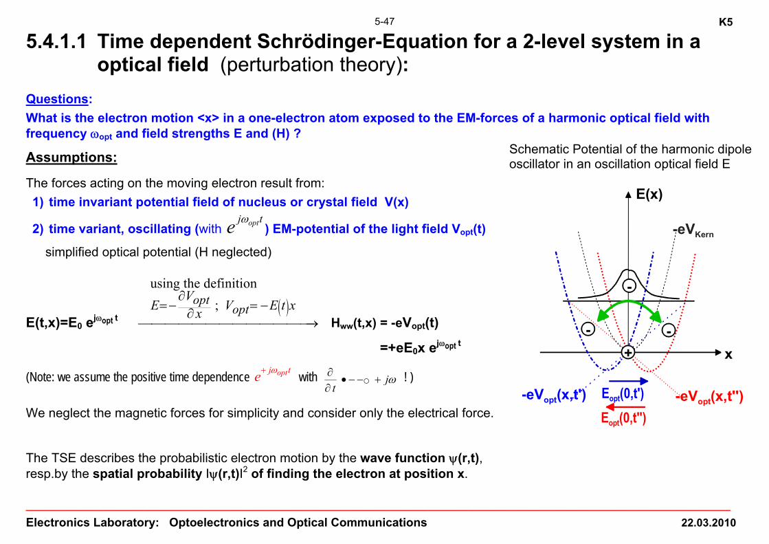
5.4.1.1 Time dependent Schrödinger-Equation for a 2-level system in a optical field (perturbation theory):
Questions:
What is the electron motion <x> in a one-electron atom exposed to the EM-forces of a harmonic optical field with frequency ωopt and field strengths E and (H) ?
Assumptions:
The forces acting on the moving electron result from:
1) time invariant potential field of nucleus or crystal field V(x)
2) time variant, oscillating (with optj te ω) EM-potential of the light field Vopt(t)
simplified optical potential (H neglected)
E(t,x)=E0 ejωopt t ( )
using the definition ;opt
optV
E V E t xx⎯⎯⎯⎯⎯⎯⎯⎯⎯⎯⎯⎯⎯→
∂= − = −∂
Hww(t,x) = -eVopt(t)
=+eE0x ejωopt t
(Note: we assume the positive time dependence optj te ω+ with jt
ω∂• − − +
∂○ ! )
We neglect the magnetic forces for simplicity and consider only the electrical force. The TSE describes the probabilistic electron motion by the wave function ψ(r,t), resp.by the spatial probability Iψ(r,t)I2 of finding the electron at position x.
Schematic Potential of the harmonic dipole oscillator in an oscillation optical field E
x
E(x)
+
-eVopt(x,t') -eVopt(x,t'')Eopt(0,t'')Eopt(0,t')
-eVKern
-
--

K5
______________________________________________________________________________________________________________________________
Electronics Laboratory: Optoelectronics and Optical Communications 22.03.2010
5-48
Time dependent Schrödinger-equation:
( ) ( ) ( ) ( ) ( ) ( )pot WWH t,x x,t H x H t,x x,t i x,tt
∂⎡ ⎤Ψ = + Ψ = Ψ⎣ ⎦ ∂ H=Hamilton-Energy –Operator, Hpot >>HWW
Hww(t,x) is the Hamilton-Operator of the optical field. 2 is the upper excited level, 1 is the lower ground state with E2 > E1.
Stationary solutions (Hww=0): ( → discrete energy levels without the optical field)
( ) ( ) ( )
( ) ( )
WW
1 2
w
without an optical field: H =0
H x,t i x,t E x,t time independent Schrödinger equationt
H x E xwith the two stationary solutions (eigenfunctions) and the energy-eigenvalues: E , E
Eigenfunctions for H
μ μ
∂Ψ = Ψ = Ψ
∂
→ =
( ) ( ) ( )( ) ( ) ( )
1
2 2
w
; E /
; /
0
E
=
=
=
1 1
2 2
-jE / h t -jω t1 1 1 1 1
-jE / h t -jω t2 2 2 2
E : Ψ x,t = u x e = u x e ω
E : Ψ x,t = u x e = u x e ω
( )
( ) ( ) ( ) ( ) ( ) ( ) ( )
i
k l kl k k kk k l klk `l
The solutions u x fulfill the
u x u x dx , u x u x dx 1 , u x u x dx 0 without prove
:
∗ ∗ ∗
≠
= Δ = Δ = = Δ =∫ ∫ ∫
Orthonormalization Relations (orthogonal and normalized)
( ) ( ) ( )2 2
1 2 i i
The stationary total solution for the 2-level-system is a superposition:
with C C 1 , E /ω+ = =
1 2-jω t -jω t1 1 2 2Ψ x,t = C u x e + C u x e

K5
______________________________________________________________________________________________________________________________
Electronics Laboratory: Optoelectronics and Optical Communications 22.03.2010
5-49Interpretation: IC1I2, (IC2I2) is the probability of finding the electron in the state E1 (E2) resp. ( ) ( )( )1 2x,t , x,tΨ Ψ . C1 and C2 are constants for the stationary state, Hww=0.
System in Ground state: C1=1, C2=0 System in Excited state: C2=1, C1=0 System in Mixed state: C2≠0, C1≠0
5.4.1.2 Optical Perturbation calculation of the transition probability rij or transition rate Rij
1) Non-stationary solution for a harmonic perturbation HWW≠0:
( ) ( ) ( ) ( ) ( )
( ) ( )
pot WW
1 2
H x,t H x H t x,t i x,tt
with the postulated solution as a superpostion of the stationary ground and excited states described by C t , C t as time functions
∂⎡ ⎤Ψ = + Ψ = Ψ⎣ ⎦ ∂
( ) ( ) ( ) ( ) ( )
( ) ( )
1 2j t j t1 1 2 2
2 21 2
x,t C t u x e C t u x
wit t
e
h C C t 1
ω ω− −
+
Ψ = +
=
The perturbation of the 2-level-system by the optical field (switched on at t=0 with eg. the system initially in the ground state IC1(0)I2=1 and IC2(t)I2=0) causes an absorption Process E1 → E2 changing the occupation probabilities IC1(t)I2 and IC2(t)I2.
For simplicity the system is at t=0 in a „pure“ state, either at E1 (leading to absorption) or at E2 (leading stimulated emission).
K5
______________________________________________________________________________________________________________________________
Electronics Laboratory: Optoelectronics and Optical Communications 22.03.2010
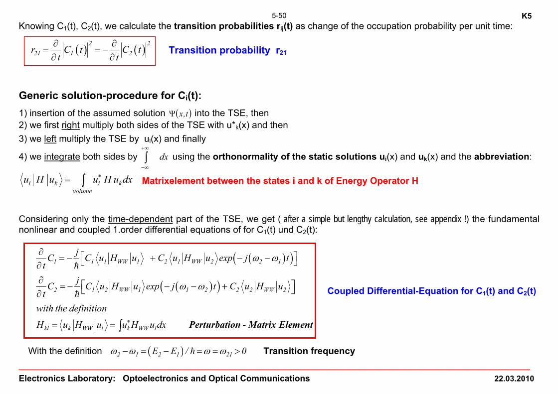
5-50Knowing C1(t), C2(t), we calculate the transition probabilities rij(t) as change of the occupation probability per unit time:
( ) ( )
2 221 1 2r C t C t
t t∂ ∂
= = −∂ ∂
Transition probability r21
Generic solution-procedure for Ci(t):
1) insertion of the assumed solution ( )t,xΨ into the TSE, then 2) we first right multiply both sides of the TSE with u*k(x) and then
3) we left multiply the TSE by ul(x) and finally
4) we integrate both sides by dx+∞
−∞∫ using the orthonormality of the static solutions ui(x) and uk(x) and the abbreviation:
i k i kvolume
u H u u H u dx∗= ∫ Matrixelement between the states i and k of Energy Operator H
Considering only the time-dependent part of the TSE, we get ( after a simple but lengthy calculation, see appendix !) the fundamental nonlinear and coupled 1.order differential equations of for C1(t) und C2(t):
( )( )
( )( )
1 1 1 WW 1 2 1 WW 2 2 1
2 1 2 WW 1 1 2 2 2 WW 2
kl k WW l k WW l
jC C u H u C u H u exp j tt
jC C u H u exp j t C u H ut
with the definition
H u H u u H u dx
ω ω
ω ω
∗
∂ ⎡ ⎤= − + − −⎣ ⎦∂∂ ⎡ ⎤= − − − +⎣ ⎦∂
= = ∫ Perturbation - Matrix Element
Coupled Differential-Equation for C1(t) and C2(t)
With the definition ( )2 1 2 1 21E E / 0ω ω ω ω− = − = = > Transition frequency

K5
______________________________________________________________________________________________________________________________
Electronics Laboratory: Optoelectronics and Optical Communications 22.03.2010
5-51
Observe that Matrix element <ukIHwwIul> is the key parameter containing the materials parameter and the optical perturbation with the frequency ωopt because Hww=Hww(E0, ωopt).
<ukIHwwIul> contains only the spatial parts ui(x) of the solutions Ψ(x).
2) Calculation of the Interaction Hamilton Operator HWW(x,t) for monochromatic harmonic optical fields:
We calculate the interaction hamiltonian Hww(t,x) as the time dependent potential energy - eVopt(x,t) of a bound electron in the time dependent potential of the electrical field strength E(t) of the harmonic optical field (magnetic energy is neglected).
The matrix element Hkl. describes the atomic forces acting on the electron inducing the transition k ↔ i resp. 2 ↔ 1. Potential energy of electrons in the optical E-field (atomic nucleus at x=0):
On atomic dimension (few Å) the optical field is considered spatially constant E(x,t)~E(0,t).
( ) ( )
( ) ( ) ( )opt
WW opt
V x,t x E 0,t
H t,x eV t,x e x E 0,t
≅ − →
= − = because ( ) ( ) ( ) ( ) ( )x
electrical ,opt opt0
F x eE x and V x E x dx E 0,t x= − = − = −∫
Considering only harmonic optical fields with frequency ωopt:
( ) ( ) ( ) ( )0 0 01 1cos exp exp2 2
optj topt opt optE t E t E j t j t E e ccωω ω ω +⎡ ⎤⎡ ⎤= = + − = +⎣ ⎦ ⎣ ⎦ Remark: we just use the positive frequency optj te ω+
-term
( )ww 0 optH t ex E cos tω= Interaction-Hamiltonian
The atomic resonance occurs at the transition frequency: 2 112 2 1 opt
E Eω ω ω ω ω−= = = − ≅
Inserting Hww(t) into the differential equation for the coefficients C1(t) und C2(t) we obtain:

K5
______________________________________________________________________________________________________________________________
Electronics Laboratory: Optoelectronics and Optical Communications 22.03.2010
5-52
( )
kl k WW l k WW l 0 opt k kVol
k l k l
11 22
using H u H u u H u dx eE cos t u x u Interaction Hamiltonian
and the definition : u x u u x u dx k l
leading to : H H 0 because x is an odd function
ω∗
∗
= = =
= ↔
= =
∫
∫ dipole matrixelement of the transition
Inserting Hww and ω21=ω in the diff. equation for Ci
( )( ) ( )( )
( )( ) ( )( )
1 opt opt 2 1 0 2
2 opt opt 1 2 0 1
jC exp j t exp j t C u eE x u ;t 2
jC exp j t exp j t C u eE x ut 2
ω ω ω ω
ω ω ω ω
∂ ⎡ ⎤= − + − +⎣ ⎦∂∂ ⎡ ⎤= + + − +⎣ ⎦∂
Coupled differential equation for C1(t) and C2(t) for harmonic optical excitation Remark: Ci(t) is determined by ω21, ωopt and 2 0 1u eE x u
For the calculation of the transition (↑, ↓) rates we will solve this diff. eq. for 2 different situations (initial conditions):
1) Switching on the field at t=0 if the system is initially either - in the ground state 1 (C1(0)=1) → absorption, upward transition or → r12 - in the excited state 2 (C2(0)=1) → stimulated emission, downward transition → r21
3) Calculation of the photon absorption (ground state transition 1 2):
we simplify the solution for C1(t), C2(t) for a weak perturbation (only small changes from the initial condition at t=0 !) of the system, which is assumed to be initially in the ground state.
1) Initial condition for Absorption: ( ) ( )21C 0 1 ground state, C 0 0= = E2>E1
2) the changes of C1(t) and C2(t) are still small with respect to the initial state, C1(t)~1-ε , C2(t)~ε <<1

K5
______________________________________________________________________________________________________________________________
Electronics Laboratory: Optoelectronics and Optical Communications 22.03.2010
5-53
With these simplification a simple integration t
0dt'∫ of the differential eq. for C2(t) leads to simple solution (appendix):
( ) ( )( ) ( )( )
opt2 2 0 1 opt
opt
sin t / 2jC t u eE x u exp j t / 22 / 2
ω ωω ω
ω ω
⎡ ⎤−⎣ ⎦= −−
and
( )
( )( )
( )2
2 opt2 222 2 0 1 0 22 2
opt
sin t / 21C t u eE x u ~ E Intensity I ; C t 14 / 2
ω ω
ω ω
⎡ ⎤−⎣ ⎦= ≈ <<⎡ ⎤−⎣ ⎦
Approximation for a weak perturbation

K5
______________________________________________________________________________________________________________________________
Electronics Laboratory: Optoelectronics and Optical Communications 22.03.2010
5-54
Approximation of the evolution of the occupation probability IC2(t)I2 of the excited state at E2:
(excitation with both exactly defined optical frequency ωopt and transition frequency ω of the 2-level system, unphysical )
The occupation probability IC2(t)I2 of the excited state 2 increases resulting in absorption. The evolution of IC2(t)I2 depends on time t and frequency detuning ω-ωopt between transition and monochromatic E-field.
• only close or at resonance ω≈ωopt there is a substantial absorption
• at resonance ω=ωopt the occupation probability of the excited state increases with t2 (experimental ~t !) → unphysical, in most experimental situations, because state energies E and photon energies hωopt need to be exactly
defined over long times without any perturbation.
• at resonance optω ω= ( )2 2 22 20
2 2 12e EC t u x u t
4= increases ~t2, the „width“ of the resonance decreases as Δω ~2π/t,
the area under the curve ( ) 22C t increases ~2πt ( constant rate at constant field).
ICI2
1 _
t 0
IC1I2
IC2I2
weak perturbation limit
~2π/ t
~t2
area ~2πt
resonance
IC2(t)I2
IC2(t)I2
δ(ω−ωopt) t
ω-ωopt ω-ωopt
t
~t2

K5
______________________________________________________________________________________________________________________________
Electronics Laboratory: Optoelectronics and Optical Communications 22.03.2010
5-55
4) Fermi’s Golden Rule
To get out of the dilemma we use a procedure known as “Fermi’s Golden Rule”:
• The calculation contains the unphysical assumptions 1) the light field is ideal monochromatic, characterized by a δ-function for the SDF W(ω) (infinite duration of the light wave !) 2) the energy levels Ei are defined exactly and characterized by a δ-function for the density of state function (assuming infinite duration of atomic states no collisions, dephasing processes, etc.). In reality the density of state function of the electrons is broadened and Ψi shows an energy ΔEi uncertainty due to the short (~0.1ps) lifetime of the state
Solution: Averaging the transition probabilities over the optical power density ρopt(ω)=W(ω)
We average the transition functions over the energy width of the optical field or the electronic states by an integration over the frequency domain of C2(t,ω)
For averaging over the optical spectral width of the transition we replace the field amplitude term E0
2 by the spectral energy
density ρopt , defined with the relation ( )20 opt opt optE / 2 ... dε ρ ω ω= ∫ , and integrate the time-dependent probability ( ) 2
optC t ,ω
weighted by ρopt(ωopt) over the finite spectral width of W(ω)=ρopt(ω) of the field:
( ) ( ) ( )( )
( )22 2 22 optopt opt22 2 1 opt 2 12 2 2
opt
opt optlim
sin t / 22W WeC t u x u d e u x u/
t
4t
2
2
2
+∞
−∞
⎯⎯⎯⎛ ⎞⎜ ⎟⎝ ⎠
⎯⎯⎯→→
⎡ ⎤−⎣ ⎦= =⎡ ⎤−⎣
−
⎦∫
ω ω π δ ω ω
ω ωω ω πωε εω ω
the averaged occupation probability increases linear with t leading to a constant transition probability r12 which is proportional to the spectral energy density W(ω)=ρopt(ω).

K5
______________________________________________________________________________________________________________________________
Electronics Laboratory: Optoelectronics and Optical Communications 22.03.2010
5-56
a) the term dipole matrixelement 12 uxu contains the dynamic microscopic properties of the 2-level system
b) a transition with a matrix element 12 uxu =0 is not possible and is called forbidden transition.
c) detuned transitions ωω ≠opt only show weak oscillations of IC(t)I2 → polarization mode
• Interpretation of the dipole matrix elements: k l k lu x u u x u dx∗= ∫
The dipole moment <p>=-e<x> is proportional to k lu x u . For strong polarization and absorption k lu x u has to be large, meaning that the wave functions uk and ul should reach large values at large values of x → only weakly bound electrons.
Stimulated emission proceeds in the same way but with changed initial conditions giving the same results:
( ) ( )1 2C 0 0 , C 0 1 excited state as "start" state= =
Einsteins Coefficient with an optical field of finite spectral energy density W(ω):
From ( ) ( )2 22
2 2 1 opt2e 1C t u x u 2 t
4ρ ω π
ε= averaged occupation probability (linear in time t)
Per definition the transition rate r12 per transition pair 1 → 2:
( ) ( )2 2 22
12 2 12C er u x u W BW
t 2π ω ωε
∂= = =
∂ → ( )
2 22 12
eB u x u2
πωε
=
Einstein-coefficient B for stimulated transitions (Absorption)
( )3 3 2 3 2
2 1 spont2 3 30 0
n eFrom A B A u x u 1/c 2 cω ωω τ
π π ε⎛ ⎞
= → = =⎜ ⎟⎝ ⎠
Einstein-coefficient A for spontaneous emission

K5
______________________________________________________________________________________________________________________________
Electronics Laboratory: Optoelectronics and Optical Communications 22.03.2010
5-57
Calculation of transition rates with a spectral energy density: (self-study)
In order to avoid the averaging by the Fermi-Golden Rule we consider that the optical field is not monochromatic but described by a spectral power density ρopt(ω). For being able to work with Fourier-transforms we consider all signal to be time-limited (compare chap.7).
The optical field amplitude is described by a time-limited envelop-function A(t) and we consider a the situation of absorption:
[ ]
( ) ( ) ( ) ( )
( ) ( )
( ) ( ) ( )
opt opt
21
j t j tTT T
1
j t2
time-limited field to the interval 0,T :
A tE t e e for 0 t T ; E t 0 for T t and t 0
2Differential equation for occupation probability for absorbtion with C t 1: p.49
jeE t jeA tC t 1 x 2 e 1 x 2 e
t 2
ω ω
ω
−
+
= + < < = < <
≈
∂= =
∂( ) ( )( )
( ) ( ) ( )
( ) ( ) ( ) ( ) ( ) ( ) ( )
21 opt 21 opt
21 opt 21 opt
j t j t
1 2 21 2 1
T
0
T Tj t j t
2 2 20 0
e
Initial condition : C 0 1 ; C 0 0 ; E E /
Integrating both sides over t: dt and considering time-limited functions:
jeC T C 0 C T 1 x 2 A t e dt A t e dt2
ω ω ω ω
ω ω ω ω
ω
+ + + −
+ + + −
+
= = = −
⎛ ⎞− = = + =⎜ ⎟
⎝ ⎠
∫
∫ ∫
( ) ( ) ( )
( )
( ) ( )
( )
( ( ) ( ) )21 opt 21 opt
T 21 optT opt21
j t j t2 T T T 21 opt T 21 opt Mixed
products =00 `0
Fourier Transform AFourier Transform A
je je jeC T 1 x 2 A t e dt 1 x 2 A t e dt 1 x 2 A A2 2 2
ω ω ω ω
ω ωω ω
ω ω ω ω+∞ +∞
+ + + −
−∞ −∞≈ ≠
− −+−
= + = + + − ⎯∫ ∫
( ) ( ) ( ) ( ) ( )2
2 22 T 21 opt T 21 opt T 21 opt T 21 opt2
0
eC T 1 x 2 A A A A4
ω ω ω ω ω ω ω ω∗ ∗
≈
⎯⎯⎯⎯→
⎛ ⎞= + + + − −⎜ ⎟
⎝ ⎠
( ) ( ) ( ) ( ) ( ) ( ) ( )
( ) ( )
2T T T T T T TT0 0
2 22 2 2
2 op2 2
Using the relation between sectral power density and spectral amplitude density (chap.7):
2 1E S d lim E E d if T S T 2 E E one sidedspectrumT 2
e eC T 1 x 2 S T 1 x 22 2
ω ω ω ω ω ω π ω ωε π
π πω ρε ε
+∞ +∞∗ ∗
→∞= = → ∞ = −
= =
∫ ∫
( ) ( )t same result as Fermi Golden RuleTω − −
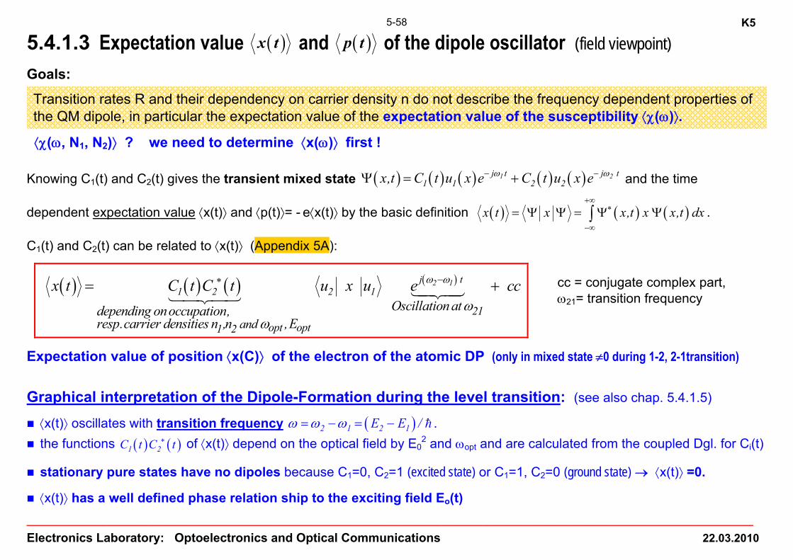
K5
______________________________________________________________________________________________________________________________
Electronics Laboratory: Optoelectronics and Optical Communications 22.03.2010
5-58
5.4.1.3 Expectation value ( )x t and ( )p t of the dipole oscillator (field viewpoint)
Goals:
Transition rates R and their dependency on carrier density n do not describe the frequency dependent properties of the QM dipole, in particular the expectation value of the expectation value of the susceptibility ⟨χ(ω)⟩.
⟨χ(ω, N1, N2)⟩ ? we need to determine ⟨x(ω)⟩ first ! Knowing C1(t) and C2(t) gives the transient mixed state ( ) ( ) ( ) ( ) ( )1 2j t j t
1 1 2 2x,t C t u x e C t u x eω ω− −Ψ = + and the time
dependent expectation value ⟨x(t)⟩ and ⟨p(t)⟩= - e⟨x(t)⟩ by the basic definition ( ) ( ) ( )x t x x,t x x,t dx+∞
∗
−∞
= Ψ Ψ = Ψ Ψ∫ .
C1(t) and C2(t) can be related to ⟨x(t)⟩ (Appendix 5A):
( ) ( ) ( ) ( )2 1j t1 2 2 1
21opt opt1 2 and
Oscillation atdepending onoccupation,resp.carrier densities n ,n ,E
x t C t C t u x u e ccω ω
ωω
−∗= +
Expectation value of position ⟨x(C)⟩ of the electron of the atomic DP (only in mixed state ≠0 during 1-2, 2-1transition)
Graphical interpretation of the Dipole-Formation during the level transition: (see also chap. 5.4.1.5)
⟨x(t)⟩ oscillates with transition frequency ( )2 1 2 1E E /ω ω ω= − = − . the functions ( ) ( )1 2C t C t∗ of ⟨x(t)⟩ depend on the optical field by E0
2 and ωopt and are calculated from the coupled Dgl. for Ci(t)
stationary pure states have no dipoles because C1=0, C2=1 (excited state) or C1=1, C2=0 (ground state) → ⟨x(t)⟩ =0.
⟨x(t)⟩ has a well defined phase relation ship to the exciting field Eo(t)
cc = conjugate complex part, ω21= transition frequency

K5
______________________________________________________________________________________________________________________________
Electronics Laboratory: Optoelectronics and Optical Communications 22.03.2010
5-59
Dipole oscillation for the transition between a symmetric ground state (u100)- and a nonsymmetric excited state (u210) of the H-Atom:
Consider the total mixed wave function ( )z,tΨ and ( ) 2z,tΨ , where we moved the phase factor out of the bracket expression:
<p(tn)> <p(tn’)>
( )' z,tΨ and ( ) 2z,tΨ at times tn (b)
( ) j2 nn b a bat 2 n / nT , n 0,1,2,3 ... phase term e 1ππ ω ω −= − = = → =
(c)
( ) ( ) ( )( )
n b a ba
j 2n 1
t ' 2n 1 / n 1 T , n 0,1,2,3...
phase term e 1π
π ω ω− +
= + − = + =
→ = −
+ +- - Dipole-oscillation occur only during the transition between 100 ↔ 210.
symmetric / anti-symmetric wavefunction
The transient mixed state ψ(z,t) is asymmetric and forms a oscillating charge dipole <p> with the transition frequency ωba=ωb−ωa
ground state excited state
( ) ( ) ( ) ( ) ( )
( ) ( ) ( ) ( ) ( ) ( )
( ) ( )
a
a b
bbb
j t j ta 100 b 210
j t j ta 100 b
j t210
2 2'
x,t C t u x e C t u x e
e C t u x C t u x e ' x,t
where x,t ' x
e
,t
ω ω
ω ω
ω ω− −
− −
− −
Ψ
Ψ = +
⎧ ⎫⎪ ⎪= + = Ψ⎨ ⎬⎪ ⎪⎩ ⎭
Ψ = Ψ
Phase term oscillating with the transition frequency ωa-ωb
mixed state

K5
______________________________________________________________________________________________________________________________
Electronics Laboratory: Optoelectronics and Optical Communications 22.03.2010
5-60Remark:
the electron charge distribution ~ uiui* is symmetric to the nucleus for a pure state, therefore stationary pure states have no dipole moment (für ρopt=0). The phase of the dipole relative to the exciting field depends on the relative phase of Ci resp. carrier occupation n2, n1 and the opt. Frequency ωopt Depending on the phase the dipole absorbs or emits radiation.
5.4.1.4 Dipole-Matrix-Elements for allowed and forbidden transitions
Possible Dipole-Matrix-Elements of a 2-level system:
The time invariant potential V(x) has been assumed as symmetric around x=0 for our 1-dimensional case. Therefore the solutions u(x) are either symmetric or anti-symmetric. However the probability density uu*(x) must be symmetric.
The dipole operator x in 12 uxu is a asymmetric function, therefore we have 4 possibilities: Initial state: final state: transition: u1 symmetric - u2 symmetric → forbidden, because 12 uxu =0 u1 asymmetric - u2 asymmetric → forbidden, because 12 uxu =0 u1 symmetric - u2 asymmetric → allowed, because 12 uxu ≠0 u1 asymmetric - u2 symmetric → allowed, because 12 uxu ≠0

K5
______________________________________________________________________________________________________________________________
Electronics Laboratory: Optoelectronics and Optical Communications 22.03.2010
5-61
5.4.1.5 QM-calculation of the Susceptibility ⟨χ(ω)⟩
Procedure: we show that the quantum-mechanical expectation value of ⟨x(t)⟩ leads to the same differential equation of motion as for the classical oscillator for x(t).
The important difference is that ⟨x(t)⟩ depends on the populations n1 and n2, and the initial occupation state leading to negative absorption, resp. gain.
For the analysis we consider the stationary harmonic solutions of the differential equation for C1(t) and C2(t) with weak harmonic optical excitation.
Calculation of the expectation value of the “dipole distance“ ⟨x(t)⟩, resp ⟨X(ω)⟩ determines the quantum mechanical Susceptibility ⟨χ(ω)⟩.
Classical mechanics: ( )0 0 0 0 01 rD E P E E E Eε ε ε χ ε χ ε ε= + = + = + = (electrons on springs)
Quantum mechanics: ( ) ( ) ( ) ( ) ( ) ( )0 0 0 0 0D E P E eN X E E eN / Xω ε ω ε ω ε ε χ ω χ ω ε ω= + = + = + → =
expectation values of physical observables Solution-Procedure:
To calculate the quantum mechanical susceptibility ⟨χ(ω)⟩, we determine from the diff.eg. for C1 and C2 first an oscillator equation of motion for ⟨x(t)⟩, resp. ⟨X(ω)⟩ having the same form as the classical diff.eq. for x(t):
( )20 D e xx x x e / m E cos tω γ ω+ + = − classical driven oscillator with damping γD and resonance frequency ω0.
1) from the oscillator differential equation of ⟨x(t)⟩ we calculate ⟨χ(ω)⟩, resp. ⟨n(ω)⟩, ⟨k(ω)⟩ as for x(t).
Definitions and assumptions:

K5
______________________________________________________________________________________________________________________________
Electronics Laboratory: Optoelectronics and Optical Communications 22.03.2010
5-62
( ) ( )
( ) ( )( ) ( ) ( )( )
opt opt
o
opt
pt opt
j t j t0
j t j t0 0opt op
j t
t
+
Definition of position expectation value : x x,t x x,t dx
EE t e e assuming: harmonic optical field with positive frequency 2
EP t e e harmonic polariz2
e ω ωω
ω ωε χ ω χ ω
∗
+ −
+ −
< >= Ψ Ψ
= +
= + −
∫
( )ation assumption
( ) ( ) ( )( ) ( ) ( )
opt opt
1 2
j t j t0ww
j t j t1 1 2 2
EH t ex E t ex e e2
x,t C t u e C t u e assumed solution for harmonically perturbed wavefunction
ω ω
ω ω
+ −
− −
= = +
Ψ = +
Therefore the differential equations for C1 , C2 (p. 5-42) transform to:
( )( ) ( )( )
( )( ) ( )( )
01 2 1 opt opt 2
02 2 1 opt opt 1
E ej C u x u exp j t exp j t C2E ej C u x u exp j t exp j t C2
ω ω ω ω
ω ω ω ω
•
•
⎡ ⎤≅ − + − +⎣ ⎦
⎡ ⎤≅ − − + +⎣ ⎦
with C Ct
∂=
∂
By insertion of the of assumed solution for ψ(x,t) into <x> we obtain:
( ) ( ) ( ) ( )j t j t1 2 1 2 1 2 1 2
2 1
x C t C t u x u e C t C t u x u e
with transition frequency:
ω ω
ω ω ω
∗+∗ ∗< >= +
= − (used p.5-49)
For the derivation of the QM-equation of motion of ⟨x(t)⟩ we evaluate the first and second derivatives x xt
∂< >= < >
∂
2
2and x xt
∂< >= < >
∂ (see appendix Chap.5). Making use of the above differential equation for C1(t) and C2(t) gives finally an:

K5
______________________________________________________________________________________________________________________________
Electronics Laboratory: Optoelectronics and Optical Communications 22.03.2010
5-63
QM Oscillator-Equation of the expectation value ⟨x(t)⟩:
(without damping force!)
fundamental driven oscillator equation for ⟨x(t)⟩ with the self-resonance ω=ω21
( ) ( ){ }1 1− ≤ ≤2 2
2 1C t - C t depends on the occupation n1, n2 of E1, E2 determines the phase of the DP to the driving E-field
F-transforming gives: x(t) → X(ω)=F(x(t)) → (frequency domain with undamped resonance at ω)
Remark: Incomplete solution, because we do not know the time-dependence of C(t) ! The equation simplifies (C ~ constant and known) under the assumption of
1) a weak field, that does not change the initial condition for C1 and C2 substantially during time t and
2) that the system was initially eg. in the ground state E1 (absorption process):
( ) ( ) ( )tCtCund1tC 211 >>≅ → medium is absorbing ( ) ( ){ } 1−∼2 22 1C t - C t
Quantum mechanic equation of oscillation for the charge position <x> for ABSORPTION (C2(t)~0, C1(t)~1)
( )22 02 1 opt
E ex x 2 u x u cos tω ω ω< > + < > = − undamped driven oscillator for absorption
Inphase or antiphase oscillating DP (classical situation)
( ) ( ) ( ){ }22 02 1 opt
E ex x 2 u x u cos tω ω ω ×< > + < > =2 2
2 1
determines the phase of the oscillator relative to the driving optical field
C t - C t
( ) ( ) ( ){ }202 12 2
opt
2E eX u x uωωω ω
⎛ ⎞= ⎜ ⎟− ⎝ ⎠
2 22 1C t - C t

K5
______________________________________________________________________________________________________________________________
Electronics Laboratory: Optoelectronics and Optical Communications 22.03.2010
5-64 → (frequency domain solution for absorption)
The QM-equation for the harmonic oscillator <x(t)> for absorption is formally equivalent to the classical undamped dipole, therefore all relations for the frequency dependence of the real part-(χ‘) and imaginary part (χ‘‘) of the QM-susceptibility <χ> will be equal (no damping γD=0). Substitution / equivalence classical ↔ QM: (absorption)
classical: Quantum mechanical dipole:
( )
( )
( )
0 2 1
20x 2 1
e
D D
E E /e E eE 2 u x u absorption, gain :
m0 undamped no loss, gain
ω ω
ω
γ γ
→ = −
− → − +
→ = →
h
Depending if the system is initially in the a) ground state (absorption) or b) excited state (emission), there is a change in the sign of the driving field in the oscillator equation (dipole phase relative to the optical field E):
a) ground state: ( ) ( ) ( ) ( )( )2 21 2 2 1C 0 1, C 0 0 C 0 C 0 1= = → − ≅ − Absorption (n1~N , n2~0)
b) excited state: ( ) ( ) ( ) ( )( )2 21 2 2 1C 0 0, C 0 1 C 0 C 0 1= = → − ≅ + Emission (n2~N , n1~0)
• the susceptibility for absorption and stimulated emission have opposite signs.
• similar to the classical case χ‘‘=0 results in no optical gain at this level of QM-oscillator model. Only by introducing damping γ we will be able to realize χ‘‘≠0.
• The necessary damping mechanism (deexcitation of excited state) by the spontaneous emission can not be introduced in the semi-classical QM-model self-consistently ( Quantization of the optical field is required).
( ) 20opt 2 12 2
opt
2E eX u x uωωω ω
⎛ ⎞= − ⎜ ⎟− ⎝ ⎠
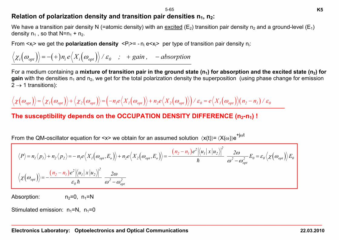
K5
______________________________________________________________________________________________________________________________
Electronics Laboratory: Optoelectronics and Optical Communications 22.03.2010
5-65
Relation of polarization density and transition pair densities n1, n2:
We have a transition pair density N (=atomic density) with an excited (E2) transition pair density n2 and a ground-level (E1) density n1 , so that N=n1 + n2.
From <xi> we get the polarization density <Pi>= - ni e<xi> per type of transition pair density ni:
( ) ( ) ( )i opt i i opt 0n e X / ; gain , absorptionχ ω ω ε= − + + −
For a medium containing a mixture of transition pair in the ground state (n1) for absorption and the excited state (n2) for gain with the densities n1 and n2, we get for the total polarization density the superposition (using phase change for emission 2 → 1 transitions):
( ) ( ) ( ) ( ) ( )( ) ( ) ( )opt 1 opt 2 opt 1 1 opt 2 2 opt 0 1 opt 2 1 0n e X n e X / e X n n /χ ω χ ω χ ω ω ω ε ω ε= + = − + = −
The susceptibility depends on the OCCUPATION DENSITY DIFFERENCE (n2-n1) ! From the QM-oscillator equation for <x> we obtain for an assumed solution ⟨x(t)⟩= ⟨X(ω)⟩e+jωt
( ) ( ) ( ) ( )
( ) ( )
221 2
1 1 2 2 1 1 opt o 2 2 opt o 0 0 opt 02 2opt
2
221 2
opt 2 20 o t
1
1
p
2
e u x u 2P n p n p n e X ,E n e X ,E E E
e u
n n
x un 2n
ωω ω ε χ ωω ω
ωχ ωε ω ω
= + = − + = − =−
=−
−
−−
Absorption: n2=0, n1=N Stimulated emission: n1=N, n1=0

K5
______________________________________________________________________________________________________________________________
Electronics Laboratory: Optoelectronics and Optical Communications 22.03.2010
5-66QM: absorption, n1=N (stimulated emission, n2=N)
( ) ( )
( )
( )
( )
221 2
opt 2 20 opt
opt
1 2
2
o 0 0 02 2opt
2
opt 2 20 opt
Ne u x u 2' ,
'' 0
with N dipole density n ; n 0 absorption
Klassisch :
Ne 2P Nex E E ' Em
Ne 2' , '' 0m
ωχ ωε ω ω
χ ω
ε χω ω
χ ω χε ω ω
= −−
=
= = =
= − = + =−
= + =−
Formal introduction of QM damping by spontaneous emission: (Appendix 5A)
Goal:
The QM-model assumed unrealistically „sharp“ energy levels and exact optical frequency meaning infinite carrier lifetimes.
As can be seen from the differential equations for C1 and C2:
An excited system can not return to equilibrium after switching-off of the optical field (E0=0) because the is no damping term in
the diff.eq. for C1, C2 (same argument as in Einstein-model) iC 0t
∂→ =
∂.
Susceptibility of the undamped, lossless QM-Dipole with density N in absorption
χ’’=0
Characteristic of χ(ω): n1>n2 (absorption)
ωopt ω
χ'(ω) χ'’(ω)=0
stimulated emission

K5
______________________________________________________________________________________________________________________________
Electronics Laboratory: Optoelectronics and Optical Communications 22.03.2010
5-67To formally introduce damping and optical gain (χ’’≠0) into the diff.eq. for C1, C2 we modify them by additional a damping term γ (representing finite carrier lifetime τ~1/γ):
Only the introduction of damping als the QM representation of loss and gain ! (from first principles required the quantization of the optical field)
( )( ) ( )( )( )
02 2 1 opt opt 1
spont
j E eC u x u exp j t exp j t Ct 2
A / 2 1 / 2 damping constant
ω ω ω ω
γ τ
∂ ⎡ ⎤= − + + − −⎣ ⎦∂
= =
2γC carrier lifetime damping of excited level E2
The damping γ relaxes C2 after a disturbance (E0 → 0) with the time constant τspont back to equilibrium i iC Ct
γ∂→ = −
∂.
We repeat the previous calculation as for the undamped case to get the frequency dependence of the susceptibility ⟨χ(ω)⟩ of the damped QM-oscillator:
( ) ( )ground state 1 excited state 2n nχ χ χ= + n1= transition pairs in ground state ; n2= transition pairs in excited state , n1 + n2 = N =atom density
( ) ( )( ) ( )
( )
( ) ( )( ) ( )
( )
( )( ) ( )
( )
2 2 22 2 opt optopt 2 1 1 22 22 2 20 opt opt
2 2 22 2 optopt 2 1 1 22 22 2 20 opt opt
2 2 D optopt 2 1 1 22 22 2 20 opt opt
2 j2eRe j Im ' j '' u x u n n2 2
2e' u x u n n2 2
2e'' u x u n n2 2
0
ω ω γ ω γωχ ω χ χ χ χ
ε ω γ ω γω
ω ω γ ωχ ω
ε ω γ ω γω
ωγ ωχ ω
ε ω γ ω γω
⎡ ⎤+ − −⎣ ⎦= + = + = −+ − +
+ −= −
+ − +
= −+ +
≠−−
using the attenuation relation from chap. 02 ''/ 2 / 1 'α β κ χ χ= ≈ − + from chap.2.
Positive frequencies have been
assumed optj te ω+
Absorption χ’’<0 Gain χ’’>0

K5
______________________________________________________________________________________________________________________________
Electronics Laboratory: Optoelectronics and Optical Communications 22.03.2010
5-68Quantum mechanically susceptibility with damping
QM allows describing optical gain as a function of population inversion (n2 > n1):
n2>n1 → Gain (for population inversion), χ“>0
n2<n1 → Attenuation, χ“<0 Real- and imaginary part of the QM-susceptibility with damping
• The frequency dependence of ( ) ( )ωχωχ '',' is similar to the classical damped dipole.
However for population inversion n2>n1 we get ( ) 0'' ≤ωχ and optical gain g(ω)= - ( )''χ ω∼
• The detuned QM-resonance frequency is:
( )/ 12 2res 2 1E E /γ ωω ω γ ω<<≅ − ⎯⎯⎯⎯→ = −
ωopt ω0
χ', χ'’
n1>n2 n1<n2
n1<n2 n1>n2
K5
______________________________________________________________________________________________________________________________
Electronics Laboratory: Optoelectronics and Optical Communications 22.03.2010
5-69
Conclusions:
• QM showed us, that the emission of a stimulated, coherent photon becomes possible for n2>n1, because the 2-level oscillator can be synchronized in such a way, that there is a dipole component orthogonal to the exciting field , resp. that χ‘‘>0. In a classic description this was not possible (χ‘‘<0).
• In case of the population inversion n2>n1 , then χ‘‘>0 and the medium produces optical gain g>0. Thus we succeeded to relate population (n2-n1) to gain and absorption.
• The stimulated global optical field E0 enforces a macroscopic synchronization of all atomic dipoles in a medium with a phase difference according to the frequency response of χ(ωopt).
• The synchronized dipoles reemit (scatter) a macroscopic dipole field, that is synchronized with the exciting field and superimposes to a 1) amplified or attenuated (χ‘’, α) and 2) phase modified (χ‘, n) total field.
K5
______________________________________________________________________________________________________________________________
Electronics Laboratory: Optoelectronics and Optical Communications 22.03.2010
5-70
Linewidth functions and reduction of maximal gain: (self-study)
For weak damping (γ>>ω) g(ω) simplifies to a Lorenzian-shaped frequency dependence L(ωopt):
( ) ( ) ( )( ) ( )
( ) ( )( )2 22 2D opt
opt opt opt 2 1 1 2 2 1 opt 1 22 22 2 20 0opt opt
2e eg '' u x u n n u x u L n n2 22
ωγ ωω α ω χ ω ω
ε εω γ ω γω≅ − = = − = −
+ − +
The width Δω of the linewidth function L(ωopt) is: ( )( ) ( ) ( )opt 2 222
21 opt 21 opt
1 1 / 4L ; 22 1 / / 2
ωω ω γγ ω ω γ ω ω ω
Δ= = Δ =
+ − Δ + −
The width of linewidth function is proportional to the inverse of the spontaneous carrier lifetime τspont (typ.~1ns for SC). Additional lifetime effects such as carrier collisions leading to a dephasing of the dipole (typ. ~100fs in SC) cause much stronger broadening and reduction of the gain by the linewidth functions.
In the following we will neglect the effect of the linewidth functions for mathematical simplicity.
Remarks:
The damping γ of the level populations n1 and n2 is the origin for the appearance of the imaginary part χ’’ of the susceptibility χ.
In the excited state the polarization is opposite to the “classical” polarization (1800 out of phase).
In the excited state the dipole acts as a source of radiation or as an active source of the field.
The role of the external stimulating field is to synchronize the phases of C1(t) und C2(t) in such a way, that there results an active dipole, emitting radiation coherent to the simulating field.

K5
______________________________________________________________________________________________________________________________
Electronics Laboratory: Optoelectronics and Optical Communications 22.03.2010
5-71
5.5 Optical band-to-band transitions in Semiconductors
In Optoelectronics active (amplifying) III-V semiconductors, such as GaAs, AlGaAs, InP, InGaAsP, GaN etc. play a key role for optical component, therefore we will concentrate on optical processes in semiconductors (SC). In the courses Physik II (3.Sem) and Bauelemente (4.Sem) it was demonstrated that the coupling of the atoms in the solid and the condensation into a periodic lattice leads to:
energetic splitting of discrete energy levels of the electrons into energy-bands (Conduction-, Valenceband) a band structure with a band gap Eg and quantized, quasi-free electron states (no localized states as in atoms) distributed, non-localized matter waves ψ(x,t) and quasi-free motion of the electrons in the bands
To analyze the optical gain in SC we extend the notion of discrete transition pairs from atoms to a quasi-continuum of state-pairs distributed over energy-bands (Conduction and Valence band) of the SC.
Similar to the averaging process for the transition rate over energy spectrum of the optical field W(ω), we assume here a mono-chromatic light field E0cos(ωot) (typical for modern optoelectronic devices) and average the transition over the energy state density distributions of the transition pairs ρcontinuum(E) or ρcontinuum(ω) (≠ρC or ρV).
Δn2
Δn1E1,ΔE1
ΔR12 ΔR21
E2,ΔE2
Conduction band: ¨
density of energy states ρC(E2) Valence band: ¨
density of energy states ρv(E1)
transition pair density ρr(E21)= ρr(ρC(E2), ρv(E1))=?
EC EV
Eg
( )2C E ,xψ
( )1V E ,xψ
ΔE2
ΔE1

K5
______________________________________________________________________________________________________________________________
Electronics Laboratory: Optoelectronics and Optical Communications 22.03.2010
5-72
Band-to-Band-Transition Rates between energy bands of semiconductors:
For SC the optical transitions occur between the densely distributed energy states Ec,i, ( )C , j xψ in the C-band and the Ev,i , ( )V ,i xψ in the V-band forming transition pairs (defined by selection rules).
For the total energy interval ΔE= ΔE2+ΔE1 we will prove later that a reduced transition-pair density (RTPD) ρr(E2-E1) can be defined as the number of transition pairs pro unit volume and unit energy ΔE.
In SC the electrons are quasi-free to move and the final state is not necessary empty as in atoms. The final state can be
occupied by an electron according to the Quasi-Fermi-occupation probability function fQ,c(E2), resp fQ,v(E1). We consider incremental sub-populations Δn2, Δn1 around the energy levels at E2 and E1 and distributed in energy intervals ΔE2 and ΔE1 with the individual density of state functions ρC(E2) and ρV(E1). Generalization of Einstein-Formalism: Conduction band Valence band
Δn2
Δn1E1,ΔE1
ΔR12 ΔR21
E2,ΔE2
Transition probability of a single transition pair Transition rate in the energy interval ΔE with the postulated pair density ρr(E12)
Stimulated Emission:
( ) ( )( )21 21 C 2 V 1
ìnitial ,occupied final ,empty
r W B f E 1 f E= −
Stimulated Absorption:
( ) ( )( )12 12 V 1 C 2r W B f E 1 f E= −
Spontaneous Emission:
( ) ( )( )21,spont 21 C 2 V 1r A f E 1 f E= −
Stimulated Emission:
( ) ( ) ( )( )21 21 r 21 c 2 v 1R W B E f E 1 f E EρΔ = − Δ
Stimulated Absorption:
( ) ( ) ( )( )12 12 r 12 v 1 c 2R W B E f E 1 f E EρΔ = − Δ
Spontaneous Emission:
( ) ( ) ( )( )21,spont 21 r 21 c 2 v 1R A E f E 1 f E EρΔ = − Δ

K5
______________________________________________________________________________________________________________________________
Electronics Laboratory: Optoelectronics and Optical Communications 22.03.2010
5-73
Transition rates rij ~ to the density of transition pairs ρr × occupation probability fi of initial state × probability of final to be empty 1-fj Generalization of transition rates for non-monochromatic light fields and distributed levels:
In the general case when optical field and transition pairs are described by spectral density functions, W(E) and ρr(E) we generalize the transition rates as for the example for the stimulated transition rate:
( ) ( ) ( ) ( ) ( )( )
( ) ( ) ( ) ( ) ( )( )
21 21 21 21 r 21 c 2 v 1
21 21 21 21 r 21 c 2 v 1
dR E B W E E f E 1 f E dE .... dE
R E B W E E f E 1 f E dE total transition rate C V
ρ
ρ+∞
−∞
= − →
= − →
∫
∫
Considered the two extreme cases:
a) optical field described by a broadband spectral density function W(Ε) and a “sharp” discrete transition-pair density N δ(E-E21) (eg. atomic states with no collision processes)
( ) ( ) ( )
( ) ( ) ( ) ( ) ( )( ) ( ) ( ) ( )( )
r 21
21 21 21 21 C V 21 21 C 2 V 1
W E ; E N E E ; N atom density
R E B W E N E E f E 1 f E dE B W E N f E 1 f E
ρ δ
δ
= − =
= − − = −∫
b) monochromatic optical field E(t)=E0cos(ωoptt) described by a spectral density function W(E)=Nphћωopt δ(E- ћωopt) and a distributed transition-pair density ρr(E) (eg. bands-to-band transition in semiconductors)
( ) ( ) ( ) ( )
( ) ( ) ( ) ( ) ( )( ) ( ) ( ) ( )( )
20 0
ph opt opt opt r ph
21 21 21 ph opt opt r C V ph opt 21 r 21 opt C 2 V 1
EW E N E E ; E ; N photon density2
R E B N E E f E 1 f E dE N B E f E 1 f E
εω δ ω δ ω ρ
ω δ ω ρ ω ρ ω
= − = − =
= − − = = −∫
Einstein-Ansatz (broad band sources)
K5
______________________________________________________________________________________________________________________________
Electronics Laboratory: Optoelectronics and Optical Communications 22.03.2010
5-74
c) monochromatic optical field E(t)=E0cos(ωoptt) with W(E)=Nphћωopt δ(E- ћωopt) and a “sharp” discrete transition-pair density N δ(E-E21)
Here the transition rate diverges because the situation is unphysical.

K5
______________________________________________________________________________________________________________________________
Electronics Laboratory: Optoelectronics and Optical Communications 22.03.2010
5-75
5.5.1 Dipole-Matrix-Element of the transitions between energy bands
For the calculation of the transition rates between valence-continuum and conduction-continuum we have to determine the dipole-matrix element
C Vu x' u between a delocalized discrete valence and a delocalized discrete conduction-band
state ( ) ( )C , j V ,ix,t and x,tψ ψ of the continuum:
→ continuum-to-continuum transition
( )( )
( )0 opt
v , j c ,ij icos tE
x,t x,tω
ψ ψ⎯⎯⎯⎯⎯→∑ ∑
In a SC the wave functions ( ) ( )C , j V ,ix,t and x,tψ ψ are extended and periodic with the lattice (lattice-modulated plane waves) The calculation of total transition rates in SC is further complicated because the transition pairs are distributed over two continuums in the conduction and valence bands
→ Summation, resp. integration over allowed band-to-band (interband) transitions ijij pairs
r−∑
Assumptions:
1) The light field is monochromatic with an amplitude E0 and a frequency ωopt resulting in a δ spectral energy density:
ρopt(ω)=1/2εEo2δ(ω − ωopt) (1-sided)
2) Wave functions in SC are non-localized Bloch-functions uj(x), having the periodicity a of the lattice.
( ) ( ) ( ) ( ) ( ) ( ) ( ) ( )j j j j 0 j j j jx,t F x u x exp jE t / resp. exp jk x u x exp jk x exp jE t /ψΨ = − = −
Fj(x) slow spatial envelope function, determined by the macroscopic crystal-potential (macroscopic crystal dimension L)
uj(x) fast varying, lattice-periodic Bloch-function, determined by the microscopic lattice potential (a lattice period a ~5A) kj(ω) crystal wave vector
0ψ normalization constant

K5
______________________________________________________________________________________________________________________________
Electronics Laboratory: Optoelectronics and Optical Communications 22.03.2010
5-76
Schematic representation of the wave function and e-h-dipoles in SC:
a = lattice period L = macroscopic crystal dimension
3) For transitions in SC the final states are not necessarily empty, but are occupied by electrons according to the Fermi-statistics F(E, EFQ) (in atoms the final state of an atomic transition-pair was per definition empty).
Dipole-transitions are represented as a superposition of wavefunctions ψC , ψV of the conduction- and valence-band.
lattice cell
. - Dipol +
Crystal-potential (schematic, period a) Wavefunctions of conduction (e) and valence band (h)
a
Lattice-periodic potential
Ek
Ej j ↔ k
extended, crystal periodic Bloch wave functions

K5
______________________________________________________________________________________________________________________________
Electronics Laboratory: Optoelectronics and Optical Communications 22.03.2010
5-77
5.6 Basic Properties of Electrons in Semiconductors (Recapitulation, 4.Sem. Hablbleiterbauelemente)
For the calculation of the rates of stimulated R21.netto and spontaneous R21,spont emission, as well as optical amplification g in SC and their relation to the electron- and hole-densities n and p we review the following basic relations on
wavefunctions in conduction (valence) band ( )c( v ) c( v )r ,k ,tψ
dispersion relation, ( )c( v ) c( v )E k
effective mass meff
density of states ( )c( v ) Eρ and
carrier densities in SC: n, p
Density of states ρc(ECi), ρv(EVi) and carrier densities n, p in conduction- and valence-band at energy Eci and Evi
Reduced density of state-pairs ρr(Eij), describing the density of electrons and holes of transition pairs having the same crystal momentum p , resp. the same propagation vector k (conservation of k of the transition) for an energy difference Eij, resp. EV1C2 : kv(Ev1)=kc(Ec2)
The dispersion relation E(ki) for electron and holes, expressing the dependence of the quantized particle energy Ei on its crystal momentum pi = ħ ki , resp. wave vector ki.
The carrier occupation probability in valence- and conduction-band described by assumed Quasi-Fermi-distribution functions fC(V)(E, EFQ) of the individual bands C, V. EFQ is the Quasi-Fermi-level of the particular band.
Quasi-Fermi-functions density of states Dispersion relation
EC(kC)
Ev(kv)
k
ρ
E E E
EC
EV
ρC
ρV
EQF,c
EQF,v fQ,v
fQ
fQ,C
EC2
EV1
kC2
kV1

K5
______________________________________________________________________________________________________________________________
Electronics Laboratory: Optoelectronics and Optical Communications 22.03.2010
5-78
5.6.1 Density of states and dispersion-relation of electrons in an ideal SC
Electrons of a precise total energy E=Ekinetic + Epotential moving in the periodic potential Vlattice(r) of a crystal can be represented quantum mechanically by a planar Bloch-wave ( )r ,tΨ as solution of the stationary Schrödinger equation.
Planar matter wave for a particle of energy E=hv, of mass m and a crystal momentum p=ħk:
( ) ( ) ( ) ( )E pr ,t u r exp j t j r u r e xp j t j k rω⎛ ⎞Ψ = − = −⎜ ⎟⎝ ⎠
u(r) has the periodicity of the crystal lattice (a)
To first order the motion of the electron in an energy band can be described as a quasi-free “classical” particle with
1) an effective mass meff, 2) a kinetic energy Ekin=E-Ec (for the electrons in the conduction band and Ekin=Ev-E for holes in the valence band) and 3) a crystal momentum p= ħk Dispersion-Relation E(k) and density of states ρ:
The kinetic energy Ekin of the electron as a quasi-free particle in the SC-crystal is related to its momentum p in the same way
as for a free particle: 2 2 2
kineff eff
p kE2m 2m
= = Bild / Formel
In analogy to classical particles there is a square law relation between the quantized crystal momentum p, resp. k and the quantized Ekin:
kp = k= wave vector of matter wave
/E=ω ω= frequency of the matter wave

K5
______________________________________________________________________________________________________________________________
Electronics Laboratory: Optoelectronics and Optical Communications 22.03.2010
5-79
the kinetic energy Ekin=E-EC of the electron is positive from the conduction band edge Ec into the band (similar for holes in the valence band)
Dispersion-Relation Ekin(k) for quantized matter waves in (1D) semiconductors:
( )
( )
( )( )
2kin
n.p
22
kinn,p
kin,n c
kin,p v
n( v )
1E p p2m
E k k2m
E E E electrons
E E E holes
m effective electron (hole) mass
=
=
= −
= − +
=
Unlike a classical particle the crystal momentum p and wave vector k are quantized ( by the boundaries of the macroscopic crystal volume Lx):
1
2 0 1 2 3
2
xx
n n x
k n n k ; n , , , , ....L
k k k / L
π
π−
= = Δ =
Δ = − =
the momentum p=ħk is quantized equidistantly by Δk=2π/Lx
Therefore also the energy levels E are quantized :
( )2 2 2
2 222kin n n
n,p x n ,p
E k k nm L m
π= = n=0,1,2,3,4 ....the energy level quantization is not equidistant !
The allowed energy-levels and momentums on the dispersions-relation E(k) are quasi-continuous, because Δk and ΔE very small.
k
Ec(k) wave vector (k) and energy (E(k)) of the quantized conduction band state Conduction band Energy gap
Valence band
EC
EV
E
E
EV(k)
V-band: Ψv,i , Ev,i , kv,i
C-band: Ψc,i, Ec,i , kc,i
Δk=2π/L momentum quantization
ΔE

K5
______________________________________________________________________________________________________________________________
Electronics Laboratory: Optoelectronics and Optical Communications 22.03.2010
5-80
Occupation of states in the k-diagram: (undoped SC → in thermal equilibrium Fermi-Energy EF lies in the band gap) Temperature T=0 Temperature T>0 (Valence band completely occupied, conduction band empty) (Valence band and conduction band partially occupied)
Bild
For each wave vector kn there are two associated energy-levels EC(kn) and EV(kn) in the conduction and valence band forming a discrete transition pair (EC(kn) ↔ EV(kn))at kn.
kn
f(E,EF) f(E,EF)
π/a −π/a −π/a π/a k a=lattice period
parabolic approximation
EF EF

K5
______________________________________________________________________________________________________________________________
Electronics Laboratory: Optoelectronics and Optical Communications 22.03.2010
5-81
Repetition: carrier densities in C- and V-bands:
In the course „Halbleiterbauelemente“ (4.Sem) the number N of solution of the Schrödinger equation in k-space has been calculated per unit volume and unit energy interval – this density is called
1. Density of states ρ(E) (DOS), resp. ρ(k) for electrons and holes as a function of Energy
ρc(E), ρv(E) using a constant effective masse for parabolic bands
( ) ( )3 / 23 / 2
pnC c V V2 2
2m2mE 4 E E , E 4 E Eh h
ρ π ρ π⎛ ⎞⎛ ⎞= − = −⎜ ⎟ ⎜ ⎟
⎝ ⎠ ⎝ ⎠
ρ describes the state density in a band at a particular energy, it does not describe the transition pair density ρr directly
2. Fermi-Occupation Probability of the energy level E by an electron
( ) ( )QFQF E E / kT
1f E,E1 e −
=+
, EQF=EF (Quasi-) Fermi-Energy of the corresponding band for equilibrium
resp. Quasi-Fermi-Distribution for electrons and holes in non-equilibrium EQF,n ≠ EQF,p
( ) ( ) ( ) ( )QF ,n QF ,pQ,n Q,pE E / kT E E / kT
1 1f E ; f E1 e 1 e− −
= =+ +
3. Electrons- and Hole-Density n, p for parabolic Bands as a function of Fermi-energies
From the DOS ρ(E) and from f(E,EQF) the carrier densities n, p are determined by integration over the corresponding band
( ) ( )
( ) ( )
C ,Top
C
V ,Bottom
v
3 / 2En,eff V F F C
c c 1 / 2 C ,eff 1 / 22E
3 / 2Ep,eff F V V F
v v 1 / 2 V ,eff 1 / 22E
1/ 2
2 m kT4 E E E En E f E dE F N FkT kTh
2 m kT4 E E E Ep E f E dE F N FkT kTh
with the Fermi Integral : F x, x
πρ
π
πρ
π
⎛ ⎞ − −⎛ ⎞ ⎛ ⎞= = =⎜ ⎟ ⎜ ⎟⎜ ⎟⎝ ⎠ ⎝ ⎠⎝ ⎠
⎛ ⎞ − −⎛ ⎞ ⎛ ⎞= = =⎜ ⎟ ⎜ ⎟⎜ ⎟⎝ ⎠ ⎝ ⎠⎝ ⎠
−
∫
∫
( )F
1 / 2
F x x0
x dx1 e
∞
−=+∫
Neff= effective density of states

K5
______________________________________________________________________________________________________________________________
Electronics Laboratory: Optoelectronics and Optical Communications 22.03.2010
5-82
4. Carrier Transport by Drift and Diffusion
n n n p p nn pj en E eD , j ep E eDx x
μ μ∂ ∂= + = −
∂ ∂
Drift current Diffusion current μ = mobility, D=diffusion constant Important for carrier transport in photodiodes and current-injection in Laser diodes and LEDs
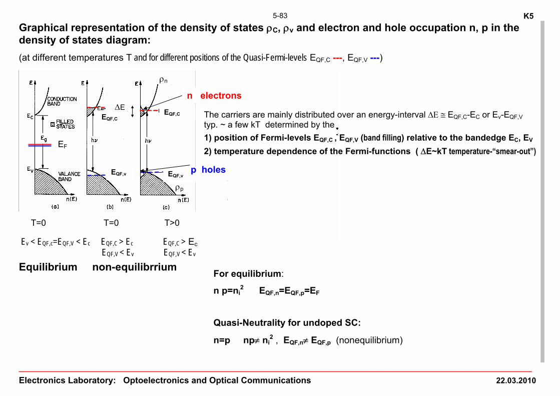
K5
______________________________________________________________________________________________________________________________
Electronics Laboratory: Optoelectronics and Optical Communications 22.03.2010
5-83
Graphical representation of the density of states ρC, ρv and electron and hole occupation n, p in the density of states diagram:
(at different temperatures T and for different positions of the Quasi-Fermi-levels EQF,C ---, EQF,V ---)
T=0 T=0 T>0 Ev < EQF,c=EQF,V < Ec EQF,C > Ec EQF,C > Ec EQF,V < Ev EQF,V < Ev
Equilibrium non-equilibrrium
For equilibrium:
n p=ni2 EQF,n=EQF,p=EF
Quasi-Neutrality for undoped SC:
n=p np≠ ni2 , EQF,n≠ EQF,p (nonequilibrium)
ΔE
ρp
ρn
EF
n electrons EQF,C
EQF,v p holes EQF,v
EQF,C
The carriers are mainly distributed over an energy-interval ΔΕ ≅ EQF,C-EC or Ev-EQF,V typ. ~ a few kT determined by the
1) position of Fermi-levels EQF,C , EQF,V (band filling) relative to the bandedge EC, EV
2) temperature dependence of the Fermi-functions ( ΔE~kT temperature-“smear-out”)
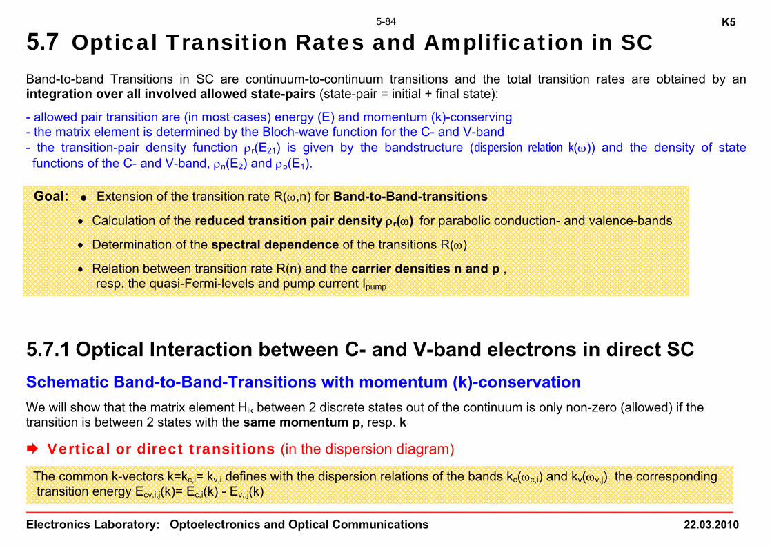
K5
______________________________________________________________________________________________________________________________
Electronics Laboratory: Optoelectronics and Optical Communications 22.03.2010
5-84
5.7 Optical Transition Rates and Amplification in SC
Band-to-band Transitions in SC are continuum-to-continuum transitions and the total transition rates are obtained by an integration over all involved allowed state-pairs (state-pair = initial + final state):
- allowed pair transition are (in most cases) energy (E) and momentum (k)-conserving - the matrix element is determined by the Bloch-wave function for the C- and V-band - the transition-pair density function ρr(E21) is given by the bandstructure (dispersion relation k(ω)) and the density of state functions of the C- and V-band, ρn(E2) and ρp(E1).
Goal: Extension of the transition rate R(ω,n) for Band-to-Band-transitions
• Calculation of the reduced transition pair density ρr(ω) for parabolic conduction- and valence-bands
• Determination of the spectral dependence of the transitions R(ω)
• Relation between transition rate R(n) and the carrier densities n and p , resp. the quasi-Fermi-levels and pump current Ipump
5.7.1 Optical Interaction between C- and V-band electrons in direct SC
Schematic Band-to-Band-Transitions with momentum (k)-conservation
We will show that the matrix element Hik between 2 discrete states out of the continuum is only non-zero (allowed) if the transition is between 2 states with the same momentum p, resp. k
Vertical or direct transitions (in the dispersion diagram)
The common k-vectors k=kc,i= kv,i defines with the dispersion relations of the bands kc(ωc,i) and kv(ωv,j) the corresponding transition energy Ecv,i,j(k)= Ec,i(k) - Ev,,j(k)

K5
______________________________________________________________________________________________________________________________
Electronics Laboratory: Optoelectronics and Optical Communications 22.03.2010
5-85
The k-conserving optical Band-to-Band-Transitions E2(k) ⇔ E1(k) in the dispersion diagram E(k): Individual dipole-transitions can only take place between wave functions of the same k-vector. Postulated momentum conservation: k of start- and final state are equal (vertical transitions)
no momentum kv ≠ kc momentum (k) kv = kc (kintial = kfinal) conservation conservatuion
forbidden allowed
Dispersions-Diagram represents energy- and momentum-conservation:
From a k the corresponding energy difference of the pair are:
( ) ( ) ( ) ( ) ( )2 2
2 2g C V g
eff ,c eff ,vE k E E k E k E k k k or k
2m 2mω ω ω= = + + = + + →
The reduced pair state density ρr has to be determined separately from the densities of states ρc , ρv.
e
h
k E(k)=ωħ=EC(k)-EV(k)
EC(k)
EV(k)

K5
______________________________________________________________________________________________________________________________
Electronics Laboratory: Optoelectronics and Optical Communications 22.03.2010
5-86
5.7.2 Direct Semiconductors
The transition rates between C- and V-band levels j and k depend essentially of the matrix-elements j ku x u . if 0uxu kj = then this optical transition is forbidden.
Transition energy ( ) ( )j j k k jk j kE E ; E E E ωΨ → Ψ = − = conserved by converting potential/kinetic energy into a radiation quantum:
kj EE −=ω Energy-conservation
During band-to-band transitions in SC the momentum of the electron-hole pair must be identical („vertical“ transitions, other transitions are forbidden):
kj kk = momentum conservation
5.7.2.1 Momentum conservation in optical transitions in undoped SC
Simple calculations will show that in ideal SC:
1) the transition matrix element is large for k-conservation and small (forbidden) for non-k-conserving transitions.
2) indirect transitions need a 3rd particle (eg. phonon) for k-conservation → low interaction probability for 3 particle interaction.
a transition is direct if the energy-minimum of the C-band and the energy –maximum of the V-band have the same k-vector
a SC with a direct optical transition (usually at k~0) is called a direct Semiconductor (eg. AlGaAs, InGaAsP, GaN, etc. but not Si, Ge)
electrons occupy the energy minimum of the conduction band and holes occupy the maximum of the valence band with high probability.

K5
______________________________________________________________________________________________________________________________
Electronics Laboratory: Optoelectronics and Optical Communications 22.03.2010
5-87
Allowed and forbidden transitions in SCs: Direct, momentum conserving transitions
To proof the k-conservation we calculate the dipole matrix-element for the electron and hole wave function in the C- , resp. V-band :
( ) ( )( ) ( )
( )
c
v
c vjk x
c,k c ,k C c
jk xv,k v ,k V v
j x
Bloch-matter wave for e and h with k vectors k , resp. k :
x u x e matter wave of e in conduction-band ; E
x u x e matter wave of h in valence-band ; E
E x e optical wave with propagatioβ
ω
ω
−
−
−
−
Ψ = =
Ψ = =
= ( )c vn vector 2 / ;β π λ ω ω ω= −
Not all transitions between ( ) ( )
c , j v ,iC ,k c , j V ,k v ,ix,k ,t x,k ,tψ ψ→ are allowed. Allowed transitions ( c , j v , ju x u 0≠ ) conserve:
1. Energy conservation: ħωopt = Ec,j – Ev,i
2. Momentum conservation: kc,j = kv,i The dipole-matrix-element of the valence-conduction band transition cv Ψ→Ψ becomes for an extended polarized (e , β ) optical plane EM-wave:
( )( ) ( ) ( )j r j t
0
Electrical plane wave : e 0 ; r x,y,z
E r E e e and E r ,t E r e ; r spatial coordinateβ ω
β− +
= =
= = =
( ) ( ){ }( )
00 0 2
j t r j r j t
E r
eEeE cos t r eE Re e e e ccω β β ωω β − − −− = = +

K5
______________________________________________________________________________________________________________________________
Electronics Laboratory: Optoelectronics and Optical Communications 22.03.2010
5-88
( ) j r0
Electrical potential :
V r ,r ' E e e r ' ; r ' dipole displacment coordinate at position rβ−= − =
Including the distributed wave and EM-wave functions in the dipole matrix elements gives integrated over the total crystal volume:
( ) ( ) ( ) ( ) ( )
( ) ( ) ( ) ( ) ( ) ( )
c v
v cc v
j r21 c ww v c 0 v 0 c v
F F 1Matrixelement
j k kjk r jk rj rc 0 v 0 c v
crystal crystalvolume volume
H r H r ,r ',t r r eE e e r ' r ,t eE u x' u
u r e eE e e r ' u r e dr eE u r u r e r ' e
β
β
ψ ψ ψ ψ∗ ∗ − ∗
= =
− − ++ −∗ − ∗
= = =
≡ =∫∫∫ ∫∫∫( )
( )( )r
0 c v
v cfalls k k 0
dr eE u e r ' uβ
β
∗
− + =
=
The function u(x) is periodic with the lattice-constant a and the exp-term containing [kC-kV-kopt]x oscillates with unity absolute value in the integral and thus the volume integral over L3 averages to <uCIxIuV>=0 if [kC-kV-kopt] ≠0 .
v c optk k 0β− + = momentum conservation in optical transitions momentum of a photon: momentum of a electron with the thermal energy Ek=kT:
4 1opt opt2 / ; 10 cmβ π λ β −= → ≈ 19e
ccc cm10kTm2
kkp −≅≈=
Because the photon wave vector kopt is much smaller than the electron-momentum c v optk ,k β>> we get:
c vk k≅ Direct Optical Transition requirement

K5
______________________________________________________________________________________________________________________________
Electronics Laboratory: Optoelectronics and Optical Communications 22.03.2010
5-89Remarks:
• The matrix element in a crystal is often a function of the optical propagation direction β , resp. of the polarization e of the optical field, therefore in SC the optical properties are often non-isotropic.
• The lattice constant (a~5Å) is much smaller than the wavelength λ (~1μm) of the light, a<<λ,. The optical field is homogenous for atomic dimensions, resp. over the lattice cell.
5.7.3 Stimulated and spontaneous transition rates in direct SC
We extended from Chap.5.5 Einstein’s-transition rates to the transition probabilities and differential transition rates in ΔE as: Conduction band Valence band
Δn2
Δn1E1,ΔE1
ΔR12 ΔR21
E2,ΔE2
Transition probability of a transition pair Transition rate in the energy interval ΔE with the pair density ρr(E12)
Stimulated Emission:
( ) ( )( )21 21 C 2 V 1r W B f E 1 f E= −
Stimulated Absorption:
( ) ( )( )12 12 V 1 C 2r W B f E 1 f E= −
Spontaneous Emission:
( ) ( )( )21,spont 21 C 2 V 1r A f E 1 f E= −
Stimulated Emission:
( ) ( ) ( )( )21 21 r 21 c 2 v 1R W B E f E 1 f E EρΔ = − Δ
Stimulated Absorption:
( ) ( ) ( )( )12 12 r 12 v 1 c 2R W B E f E 1 f E EρΔ = − Δ
Spontaneous Emission:
( ) ( ) ( )( )21,spont 21 r 21 c 2 v 1R A E f E 1 f E EρΔ = − Δ
vc2
2
uxu2
eB π=

K5
______________________________________________________________________________________________________________________________
Electronics Laboratory: Optoelectronics and Optical Communications 22.03.2010
5-90
Wave functions of electrons in bands of SC are not localized and the final state may already be occupied by a particle according to the Fermi-statistic thus blocking the transition (because of Pauli exclusion principle):
• the transition rate r12 (eg. absorption 1→2) is ~ to the probability f(E1), that the start-level E1 is occupied
• the transition rate r12 (eg. absorption 1→2) is ~ to the probability [1-f(E2)], that the final-level E2 is empty • ( ) ( )( )ij i jr f E 1 f E−∼
occupied state: empty state: fx = Fermi-Function of band x
Concept of the reduced density ( )Erρ for k-conserving pairs and the reduced mass rm :
Concept:
For optical transitions rates with k-conservation we are interested in the number of energy-pairs (in the 2 bands) with the same k-vector in the interval Δk, resp. per energy interval ΔEs at E2(k) and E1(k) in C- and V-band.
(the density of states ρn and ρp describe only the number of energy-levels (not pairs !) per energy interval ΔE in one band)
Definition of the Reduced Density ρr for transition-pairs in conduction and valence bands:
the reduced density ( )r Eρ is defined as number of energy level-pairs with the energy-difference E per energy interval ΔE where the initial and final states in the conduction and valence band have the same k-vector
eh-pair

K5
______________________________________________________________________________________________________________________________
Electronics Laboratory: Optoelectronics and Optical Communications 22.03.2010
5-91
The continuum-continuum transition rates R are proportional to the so defined reduced pair density rρ weighted by the occupation probabilities of the initial and final state-pair.
Graphical representation of continuum → continuum transitions 2 (C) 1 (V)
momentum conservation: k1 = k2
Remark: k determines (by the dispersion relation E(k)) the energy levels E2(k) and E1(k), E(k)=E2(k) – E1(k) of an individual pair
ΔN-states in Δk
ΔN-states in Δk
Δk
δk (equidistant k-quantization) → in ΔE1 und in ΔE2 we have ΔN=Δk/δk
ΔE21
ΔE1
ΔE2
Dispersion relation E(k):
2 22 c 2 nE E k / 2m− = conduction band
2 2v 1 1 pE E k / 2m− = valence band
All ΔN transition pairs of the momentum interval Δk are distributed in the total energy interval ΔE21: ΔE21= ΔE2+ ΔE1
ρC ΔΕΔΕ2
ΔΕ1
ΔΝ Uebergangspaare ρr ?
Ε1
Ε2
Δk k
E

K5
______________________________________________________________________________________________________________________________
Electronics Laboratory: Optoelectronics and Optical Communications 22.03.2010
5-92
Procedure for the calculation of the reduced density ρr:
calculate the reduced density ρr for direct transition (k2=k1) between E2 and E1 as a function of the known densities of states of conduction and valence band ρc(E2), ρv(E1) and as a function of k, resp E21:
ρr{E21}= ρr{ρc(E2), ρv(E1)} = ?
The calculation of the number of transition pairs ΔN(Δk) in the momentum interval Δk is simple, because all states are separated by the equal momentum quantization δk. We then transform the interval Δk into the associated energy interval ΔE21(Δk) with the help of the dispersion relation of the C- and V-bands.
In addition we also use the fact that ΔΝ can also be expressed by both energy state densities
ΔN=ρv(E)ΔE1=ρc(E)ΔE2 with ΔE1(Δk) ≠ ΔE1(Δk). a) Calculation of the number of transition pairs ΔN in the interval Δk and ΔE:
Due to the quantization δk of kn there are ΔN pairs in the momentum interval Δk:
knkn δ= with L/hk =δ (1-D case) , resp. 33 L/hk =δ (3-D-case)
N k / k transition pairsδΔ = Δ distributed over the total energy interval ΔE21= ΔE2+ ΔE1
ΔN transition pairs are distributed in each energy interval ΔE2 and ΔE1 at E2 and E1. b) Calculation of the relation between ΔE2 , ΔE1 , (E2-Ec) and (Ev-E1) with k and Δk:
Δk, ΔE21, ΔE2, ΔE1 are related by the dispersion relation E(k)
( )( ) ( )( )2 2
2 22 c 1 v
n p
2 2
2 1n p
differentiation by k:E k E k and E k E k ;2m 2m
E k k and E k km m
− = − + = →
Δ = Δ Δ = Δ^
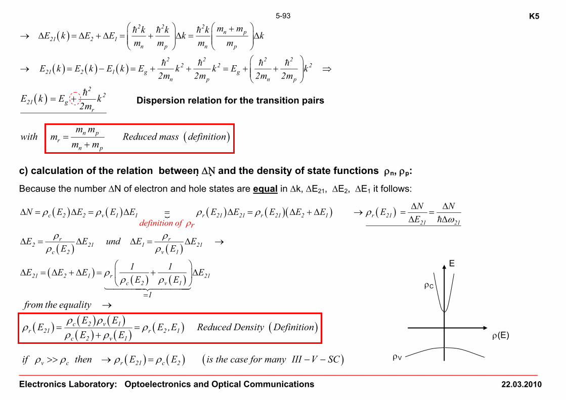
K5
______________________________________________________________________________________________________________________________
Electronics Laboratory: Optoelectronics and Optical Communications 22.03.2010
5-93
( )
( ) ( ) ( )
2 2 2n p
21 2 1n p n p
2 2 2 22 2 2
21 2 1 g gn p n p
m mk k kE k E E k km m m m
E k E k E k E k k E k2m 2m 2m 2m
⎛ ⎞ ⎛ ⎞+→ Δ = Δ + Δ = + Δ = Δ⎜ ⎟ ⎜ ⎟⎜ ⎟ ⎜ ⎟
⎝ ⎠ ⎝ ⎠⎛ ⎞
→ = − = + + = + + ⇒⎜ ⎟⎜ ⎟⎝ ⎠
( )
( )
22
21 gr
n pr
n p
E k E k2m
m mwith m Reduced mass definition
m m
= +
=+
c) calculation of the relation between ΔΝ and the density of state functions ρn, ρp:
Because the number ΔN of electron and hole states are equal in Δk, ΔE21, ΔE2, ΔE1 it follows:
( ) ( ) ( ) ( )( ) ( )c 2 2 v 1 1 r 21 21 r 21 2 1 r 2121 21definition of r
N NN E E E E E E E E E EEρ
ρ ρ ρ ρ ρω
Δ ΔΔ = Δ = Δ = Δ = Δ + Δ → = =
Δ Δ
( ) ( )
( ) ( ) ( )
r r2 21 1 21
c 2 v 1
21 2 1 r 21c 2 v 1
1
E E und E EE E
1 1E E E EE E
ρ ρρ ρ
ρρ ρ
=
Δ = Δ Δ = Δ →
⎛ ⎞Δ = Δ + Δ = + Δ⎜ ⎟
⎝ ⎠
( ) ( ) ( )( ) ( ) ( ) ( )
( ) ( ) ( )
c 2 v 1r 21 r 2 1
c 2 v 1
v c r 21 c 2
from the equalityE E
E E ,E Reduced Density DefinitionE E
if then E E is the case for many III V SC
ρ ρρ ρ
ρ ρ
ρ ρ ρ ρ
→
= =+
>> → = − −
Dispersion relation for the transition pairs
E ρC ρ(E) ρV

K5
______________________________________________________________________________________________________________________________
Electronics Laboratory: Optoelectronics and Optical Communications 22.03.2010
5-94
we get with ( )2
rNE
Vol Eρ ∂
=∂ ∂
for the Transition Rates ( )3 NR E
Vol E t∂
=∂ ∂ ∂
by generalizing to continuum (C:2) – continuum (V:1)
transition with a monochromatic field ( ) ( )( )220
21 2 1EEW E E E E
Vol E 2ε δ∂
= = − −∂ ∂
:
( ) ( ) ( )( ) ( ) ( ) ( )( ) ( )
( )( ) ( ) ( )( ) ( )
( ) ( ) ( ) ( )( )( ) ( ) ( )( ) ( )
2 2 2 2021,abs 21 c, j v,0 r 21 c 2 v 1 0 r 21 c 2 v 12
22 2c, j v,0
221,stim 21 0 r 21 V 1 C 2
221,net 21 0 r 21 C 2 V 1
21,spont 21 r 21 V 1 C 2 spont 21,spont
e ER E u x u E 1 f E f E E B E 1 f E f E2
B e / 2 u x u
R E E B E 1 f E f E
R E E B E f E f E
R E A E 1 f E f E E R dR
π ρ ε ρ
π ε
ε ρ
ε ρ
ρ
= − = −
=
= −
= −
Δ = − Δ → = =∫ ( ) ( )( ) ( )r 21 V 1 C 2A E 1 f E f E dEρ −∫
with 2 1E Eω −
=
fv, fc are the Quasi- Fermi-functions at E1 and E2 Remark:
if (E2-E1)=E21=ћω in a practical situation is specified, we get the corresponding k by solving a quadratic equation for E21(k). From k we obtain E2, E1 and ρr(E2, E1) by using the corresponding dispersion relations of the C- and V-band.

K5
______________________________________________________________________________________________________________________________
Electronics Laboratory: Optoelectronics and Optical Communications 22.03.2010
5-95Transform Eo to photon density sph of the momochromatic field:
Modern optoelectronic devices often operate with almost monochromatic fields compared to the energy width of the band-to-band transitions in SC. Therefore we use discrete field-amplitudes Eo or photon densities.
2o ph optUsing w E / 2 sε ω= =
( ) ( ) ( )221,netto opt o r 2 1 ph opt r 2 1
1R E B f f s B f f2
ω ε ρ ω ρ= − = −
( ) ( ) ( )
( ) ( ) ( )
221 r 2 1 o r 2 1 ph r 2 1
212 r 1 2 o r 1 2 ph r 1 2
1R w B f 1 f E B f 1 f s B f 1 f21R w B f 1 f E B f 1 f s B f 1 f2
ρ ε ρ ω ρ
ρ ε ρ ω ρ
= − = − = −
= − = − = −

K5
______________________________________________________________________________________________________________________________
Electronics Laboratory: Optoelectronics and Optical Communications 22.03.2010
5-96
5.7.4 Optical Amplification and Attenuation in ideal SCs Goals:
Combining the transition pair density ρr and the Fermi-functions f for the occupation probability of the energy-levels we can in principle calculate all transition rates R (at least numerically) and their frequency dependence, determined mainly by ρr(ω) and f(EF,ω):
• Emissions-/Absorption rates R21,net(ω), R21(ω), R12(ω) und R21,spont(ω) vers. ω resp λ, E21 (rates per unit volume at the optical energy ħω21 or wavelength λ21) as a function of
1) the Quasi-Fermi-Levels EFQc and EFQv or
2) the carrier densities n and p (to combine with the carrier rate equation !) because n=n(EFQc) and p=p(EFQv)
• Amplification g(ω) versus carrier density n or finally as a function of pump current: g(ω,n), resp. g(ω,I)
• Wavelength λmax(n) and value of the maximal optical gain gmax(n, λmax) These rates will be fundamental for the design of the characteristics of diode lasers and optical amplifiers in chap.6.
5.7.4.1 Gain spectrum g(ω,EQF,n, EQF,p) ; g(ω,n=p)
Procedure:
For the computation of the frequency dependence of g(ω,n=p), g(ω,EQF,n, EQF,p) the transition rates R21,net(E=ħω) , R12(E) , R21(E) , Rspont(E), R21,spont are evaluated at
a) given optical energy E=ħω, resp. a wavelength λ and
b) given quasi-Fermi-level EFQ,n, EFQ,p, resp. carrier density n(EFQ,n)=p(EFQ,p) assuming carrier neutrality
EFQ,n , EFQ,p are not independent because of the charge neutrality n=p condition (pumped undoped SC) !

K5
______________________________________________________________________________________________________________________________
Electronics Laboratory: Optoelectronics and Optical Communications 22.03.2010
5-97
Relation between optical amplification g(ω,n) and netto-rate of stimulated emission R21,netto(ω,n):
From R21,netto(ω,n) we obtain immediately the important spectral gain function g(ω,n) often used in device design.
Assuming given quasi-Fermi-energies EFQc, EFQv (with the restriction n=p) and using the fundamental relation between the gain g(ω, EFQc, EFQv ) and R21,netto
( ) ( ) ( )
( ) ( ) ( ) ( )( ) ( ) ( ) ( )( )( )( ) ( ) ( )( )
( )
ph ph21,net 21 12
ph gr ph gr ph gr ph
phFQc FQv r 21 c 2 FQ,c v 1 FQ,v r 21 v 1 FQ,v c 2 FQ,c
gr ph
r 21 c 2 v 1gr
22
21 c v20
s s1 1 1 1g R R R gs x v s t v s v s
s hvg ,E ,E B E f E ,E 1 f E ,E B E f E ,E 1 f E ,E
v s
hv B E f E f Ev
ewith B E u x u ,2
ω ω
ω ρ ρ
ρ
πε
∂ ∂= = = = − = →
∂ ∂
⎡ ⎤ ⎡ ⎤= − − − =⎣ ⎦ ⎣ ⎦
= −⎡ ⎤⎣ ⎦
= ( ) ( ) ( )r 21 21 2 1 2 1E , E E E and the relation between E and E , E we express g asρ ω ω= = − →
( ) ( ) ( ) ( ) ( ) ( )max 21 max 21 r 21gr
, 0
c 2 v 1g f Eg E EE ; g Ev
f Bωω ρ> <
⎤= −⎡ ⎦ =⎣
( ) ( )c 2 v 1f E f E−⎡ ⎤⎣ ⎦ defines pumping condition and “parabolic or bell-shaped” frequency dependence of g(ω)
For the numerical evaluation of g(ω) the energies E1(ω), resp. E2(ω), assuming k-conservation, are determined first followed by the computation of f(E2) and f(E1) using the charge neutrality n=p.

K5
______________________________________________________________________________________________________________________________
Electronics Laboratory: Optoelectronics and Optical Communications 22.03.2010
5-98
From the functional dependence of g(ω,n) some basic conclusions about the gain-spectrum can be drawn:
Condition for amplification in SC (Bernard-Duraffourgh condition) a) SC in thermal equilibrium (no population inversion)
In thermal equilibrium in undoped SC the Fermi level is approx. in the middle of the bandgap: ( )FQ ,c FQ ,v F c vE E E E E / 2= = ≅ + therefore fc(E2) < fv(E1) (few electrons in the C-band)
As a result g is negative and the SC is for all frequencies absorbing (attenuating), so stimulated absorption is the dominating rate.
( ) ( ) ( ) ( ) ( ) ( )
( ) ( )
( )
max c 2 v 1 max v 1
2 2*max c v r 21
gr
g
g g f E f E g f E
e 2with g . u x u E2 v
for E / Absorption at the Bandedge
ω ω ω
π ωω ρε
ω
= − −⎡ ⎤⎣ ⎦
≅
≈
∼
remark: here ρr is the density per energy interval !
In general we can estimate g(ω) by considering:
• for the term ( ) ( )[ ]1,vv2,cc EfEf − we have the following inequality: ( ) ( )[ ] 1EfEf1 1,vv2,cc <−<−
• the dependence of gmax(ω) is dominated by ( ) ( ) ( )3 / 22r c eff ,c gE E 4 2m / h E Eρ ρ π≅ = − ,
if ρc<< ρv as is the case for many III-V-SC
then ( ) ( )max 21 gg E E /ω ≈ − max. absorption for parabolic bands
(assuming that the matrix element is only weakly dependent on the transition energy E21)
• Optical amplification is only possible if fc(E2) >fv(E1), that means [fc(E2) -fv(E1)] >1 POPULATION-INVERSION

K5
______________________________________________________________________________________________________________________________
Electronics Laboratory: Optoelectronics and Optical Communications 22.03.2010
5-99
b) Properties of the spectral dependence of optical gain g(ω) and absorption α(ω): For simplicity we assume T=0. 1) Intrinsic SC at T=0 and in thermal equilibrium: n=ni, p=ni (no gain-situation)
( ) ( ) ( ) ( ) ( ) [ ] ( ) ( )FQ,c FQ,v F i
max c 2 v 1 max max g
E E E E
g g f E f E g 0 1 g 0 ~ E Eω ω ω ω
= = ≅
= − = − = − < −⎡ ⎤⎣ ⎦
the semiconductor absorbs at all frequencies gEω > transparency loss
Absoption becomes stronger for shorter wavelengths.
Above the bandgap wavelength the material becomes transparent.
+1
-1
Eω=(E-Eg)/ hEg
g(E)g(ω)
fC(E2)-fV(E1)
Verstärkung
Absorption
gmax(ω)
transparency
E
f(E)
EF
gain

K5
______________________________________________________________________________________________________________________________
Electronics Laboratory: Optoelectronics and Optical Communications 22.03.2010
5-100
2) Intrinsic SC at T=0 and in thermal non-equilibrium (Inversion) n>ni , p>ni but n=p (quasi-neutrality)
( )( ) ( ) ( ) ( )
( ) ( ) [ ] ( )( ) ( ) [ ] ( )
FQ,c C FQ,v V FQ,c FQ,v g
max c 2 v 1
max max g 21 FQ,c FQ,v
max max 21 FQ,c FQ,v
Assumption : E E , E E E E E degenerated SC
g g f E f E
g g 1 g for E E E E range of amplification
g g 1 g for E E E range of absorption
ω ω
ω ω ω
ω ω ω
> < → − >
= −⎡ ⎤⎣ ⎦
= + = < < −
= − = − > −
Quasi-Neutrality: n=p transparent I gain I losses/absorption
the SC amplifies in the frequency range g FQ,c FQ,vE E Eω< < − In the frequency range FQ,c FQ,vE Eω > − the SC is absorbing.
Condition for amplification in SC by Bernard-Duraffourgh
the condition FQ,c FQ,vEg E Eω< < − is called the amplification-condition of Bernard-Duraffourgh.
transparency
E
fc(E)
EFQ,c
EFQ,v
fv(E)
+1
-1
Eω=(E-Eg)/ hEg
g(E)g(ω)
fC(E2)-fV(E1)
Verstärkung
Absorption
Eg
(EFQ,c-EFQ,c)
transparency
EC EV
gain
EFQ,v
EFQ,c
E2
E1

K5
______________________________________________________________________________________________________________________________
Electronics Laboratory: Optoelectronics and Optical Communications 22.03.2010
5-101
3) Intrinsic SC at T>0 and thermal non-equilibrium (population inversion):
For T≠0 the expression for g(ω,n) is “smeared out” due to the continuous distribution of the Fermi-function at EQF. The following figure gives a qualitative picture of the role of the factor ( ) ( )[ ]1v2c EfEf − in the expression for
( ) ( ) ( ) ( )[ ]1v2cmax EfEfgg −= ωω .
Thermal broadening of g(ω): graphical construction of the spectral dependence of the gain g(ω)
ΔE ~kT transparent I gain I losses/absorption
Gain
Absorption
g(ω)Transparency
Band-filling and thermal broadening: The spectral width Δω of g(ω,n) is determined by:
• Filling of the bands by the carrier density n
• Temperature dependence of the Fermi-function
The higher the carrier density n or the higher the temperature T
- the broader the positive gain-spectrum
- the smaller the peak gain

K5
______________________________________________________________________________________________________________________________
Electronics Laboratory: Optoelectronics and Optical Communications 22.03.2010
5-102If the quasi-Fermi-levels are assumed to be known under the constraint of charge neutrality n=p, then the electron density n in the conduction band can be determined and we will calculate the gain g(ω,n) vers. carrier density n.
This dependence is essential for device design and combining g with the rate-equations. Numerical example of gain spectra g(λ,n) for GaAs and InGaAs at different carrier densities n=p:
Parameter: carrier density (electron density /1018cm3) gain is narrowband: Δλ~0.1λ Remark on densities of states and quasi-Fermi-levels: For the self-consistent calculation of g(ω,n) we have to eliminate the quasi-Fermi-levels EFQc(n), EFQv(p). As EFQc, EFQv determine n and p and together with the boundary condition of quasi-neutrality in the SC n=p, the elimination can be carried out numerically as no analytical inverse Fermi-function 1
1/ 2F − exists .
( ) ( ) ( )( )
( ) ( ) ( )( )
C ,Top
C
V ,Bottom
v
E
n n C ,eff 1 / 2 FQn CE
E
p p V ,eff 1 / 2 V FQvE
n E f E dE N F E E / kT
p E f E dE N F E E / kT
ρ
ρ
= = −
= = −
∫
∫
F1/2 are Fermi-integrals ( ) ∫∞
−+=
0xx
2/1
F2/1 dxe1
xx,xFF
n(EQF,C)=NC,eff F1/2([EQF,C-EC]/kT) and with the inverse function [EQF,C-EC]/kT= F1/2-1(n/ NC,eff)
p(EQF,V)= NV,eff F1/2([EV-EQF,V]/kT) and with the inverse function [EQF,V+EV]/kT= F1/2-1(p/ NV,eff)
gain
loss
n gain
loss
n To achieve substantial gain in SC the
“transparency” carrier density ntr
must be in the range of 3-4 1018 cm-3

K5
______________________________________________________________________________________________________________________________
Electronics Laboratory: Optoelectronics and Optical Communications 22.03.2010
5-103
5.7.4.2 Spontaneous Emission versus carrier density n and wavelength λ a) incremental spontaneous emissions rate R21,spont into all modes
In the analysis of the thermal equilibrium with the blackbody radiation, we considered the radiation equilibrium with all modes of the blackbody-radiation.
so the Einstein-coefficient A for discrete energy states describes the spontaneous emission rate into a all modes.
The incremental spontaneous emission rate ΔR21,spont(ω) for a the frequency ω, resp. energy ω=E can be calculated from
( ) ⎟⎟⎠
⎞⎜⎜⎝
⎛= 2
02
3
cBA
πωω Einstein-Relation.
• the spontaneous emission rate results from downward-transitions and has to be weighted by the level-occupancy (Fermi-functions fC and fv:
( ) ( ) ( ) ( )( ) ( ) ( ) ( )( )3
21,spont r c c,2 v v,1 r c c,2 v v,12 20
R A . f E 1 f E E B . f E 1 f E Ec
ωω ρ ω ρ ωπ
⎛ ⎞⎡ ⎤ ⎡ ⎤Δ = − Δ = − Δ⎜ ⎟⎣ ⎦ ⎣ ⎦⎝ ⎠ Spontaneous Emission in ΔE
b) Total spontaneous emission rate Rspont into all possible spatial and frequency modes:
The total spontaneous emission is generated isotropic in all directions by all transition pairs distributed over the whole energy range ΔE=ħΔωspont. For the total spontaneous emission rate Rspont we have to integrate over all filled states in the bands resp. to the carrier density n under assumption f charge neutrality n=p.
The total spontaneous emission rate Rspont enters the carrier rate-equation for n and p.
Rspont is emitted into all modes keeping in mind that Rspont >> R21,spont ,mode.
( ) ( ) ( ) ( )( )spont r c c,2 v v,1 21,spont,DEFINITION of
mode0
1R A . f E 1 f E d Rγ
ω ρ ω ωγ
∞⎡ ⎤= − =⎣ ⎦∫

K5
______________________________________________________________________________________________________________________________
Electronics Laboratory: Optoelectronics and Optical Communications 22.03.2010
5-104For lasers also need the fraction γ, β of spontaneous emission into a single mode R21,spont, mode:
( ) ( )( )spont
mode spont spont mode spont
= :
1/ V d 1/ Vω
γ β
γ ρ ω ω ρ ω ωΔ
= ≅ Δ∫
Definition of the spontaneous emissions factor ρmode = mode density of free space
If A and B are approximately frequency independent, we can use for simplicity the following
life-time approximation for Rspont:
( ) ( ) ( )( )
( ) ( ) ( )( ) ( )
spont r c c ,2 v v,1 spont0 spont
spont
spont r c c ,2 v v,10
spont
Definition ofR A f E 1 f E d n /
at high carriere densities is not really constant but depends also on n
n / A f E 1 f E 1 / n not constant !
R n
τρ ω ω τ
τ
τ ρ ω
∞
∞
⎡ ⎤= − ≈ →⎣ ⎦
⎡ ⎤= − ≈⎣ ⎦
→
=
∫
∫
( )2spont BM/ B n Bimolecular Recombinationτ ≈
Numerical calculation of Rspont(n) confirms a square-law dependence ~n2 (– n3) of the carrier density n (Bimolecular Recombination).
• the spectral width Δωspont of the spontaneous emission R21,spont(ω) is in general larger than the width Δωstim of stimulated emission Rstim(ω)
• for mathematical simplicity spontaneous emission rates are often approximated by a constant carrier lifetime τspont,tot.
Numerical Simulation of Gain- and spontaneous emission-spectra for GaAs:
Δωspont Δωstim
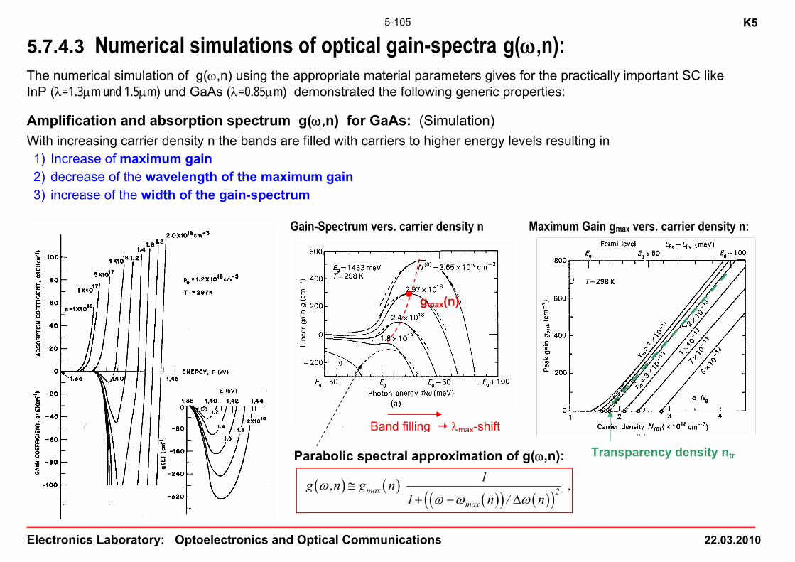
K5
______________________________________________________________________________________________________________________________
Electronics Laboratory: Optoelectronics and Optical Communications 22.03.2010
5-105
5.7.4.3 Numerical simulations of optical gain-spectra g(ω,n):
The numerical simulation of g(ω,n) using the appropriate material parameters gives for the practically important SC like InP (λ=1.3μm und 1.5μm) und GaAs (λ=0.85μm) demonstrated the following generic properties: Amplification and absorption spectrum g(ω,n) for GaAs: (Simulation)
With increasing carrier density n the bands are filled with carriers to higher energy levels resulting in 1) Increase of maximum gain 2) decrease of the wavelength of the maximum gain 3) increase of the width of the gain-spectrum
Gain-Spectrum vers. carrier density n Maximum Gain gmax vers. carrier density n:
Parabolic spectral approximation of g(ω,n):
( ) ( )( )( ) ( )( )max 2
max
1g ,n g n ,1 n / n
ωω ω ω
≅+ − Δ
gmax(n)
Band filling λmax-shift
Transparency density ntr

K5
______________________________________________________________________________________________________________________________
Electronics Laboratory: Optoelectronics and Optical Communications 22.03.2010
5-106
Linear Gain dependence for bulk semiconductors: Simulation show that the maximum gain gmax is approximately linear dependent on the carrier density n > ntr.
( ) ( )trmaxmax nnan,g −≅ω Linear approximation of max. gain in function of n
Definition: ntr = Transparency-carrier density ( ( )max max trg ,n 0ω ≅ ) and a = differential gain ( ) maxa n g / n= ∂ ∂
• at n=0 the material is absorbing with f1~1 and f2 ~0 , g(0)~ -gmax(ω) • at n=ntr (transparency density) the material is transparent , g(ntr)=0 • at n>ntr the material is amplifying with f1~0 and f2 ~1 , g(n)~ +gmax(ω)
Nonlinear gain-carrier density relation for Quantum Wells (QW) in SCs:
gmax(n) relations show in general the nonlinear behavior (logarithmic for QWs) of the figure below and a parabolic frequency dependence:
( ) ( )0max max trg ,n g ln n/ nω ≅
Parabolic approximation of the spectral dependence of g(ω,n):
( ) ( ) ( )2 2
max maxmax max trg ,n g ,n / 1 a n n / 1ω ω ω ωω ω
ω ω
⎧ ⎫ ⎧ ⎫− −⎪ ⎪ ⎪ ⎪⎛ ⎞ ⎛ ⎞= + = − +⎨ ⎬ ⎨ ⎬⎜ ⎟ ⎜ ⎟Δ Δ⎝ ⎠ ⎝ ⎠⎪ ⎪ ⎪ ⎪⎩ ⎭ ⎩ ⎭
Valid approximation because often only the gain close to the maximum is relevant !
ω
ggmax
ωmax
Δω
g(ωmax,n)
n ntr

K5
______________________________________________________________________________________________________________________________
Electronics Laboratory: Optoelectronics and Optical Communications 22.03.2010
5-107
Temperature dependence of the optical gain g(ω,n,T) in SC:
Thermal gain broadening and gain reduction
Because of the temperature T dependence of the Fermi-functions and subsequent broadening of the carrier distribution: • the spectral width Δω of g(ω,n) increases with increasing temperature • the maximum gain gmax(ωmax,n) decreases with increasing temperature (RT-operation of diode lasers was a challenge)
T=297K T=77K
Bild Temp-abhängigkeit
The broadening and reduction of the optical gain with temperature has a very detrimental effect on devices such as diode lasers and amplifiers. It is also responsible for the high temperature sensitivity of these devices.
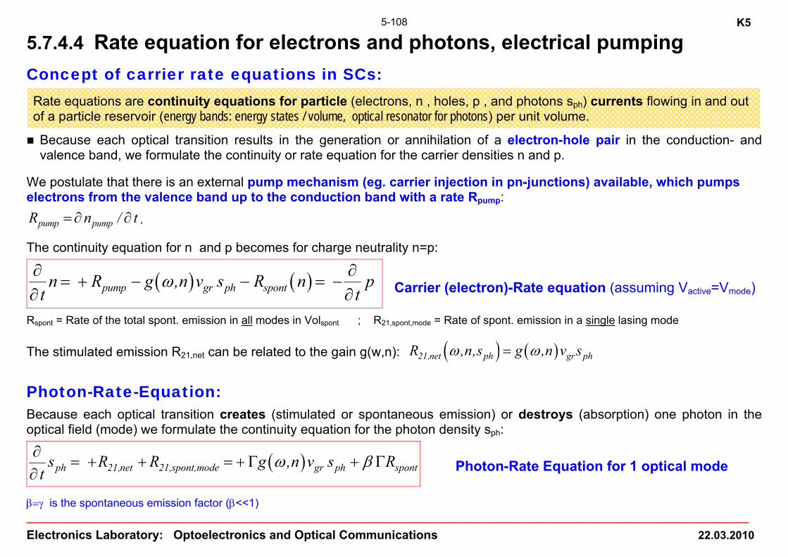
K5
______________________________________________________________________________________________________________________________
Electronics Laboratory: Optoelectronics and Optical Communications 22.03.2010
5-108
5.7.4.4 Rate equation for electrons and photons, electrical pumping
Concept of carrier rate equations in SCs:
Rate equations are continuity equations for particle (electrons, n , holes, p , and photons sph) currents flowing in and out of a particle reservoir (energy bands: energy states / volume, optical resonator for photons) per unit volume.
Because each optical transition results in the generation or annihilation of a electron-hole pair in the conduction- and valence band, we formulate the continuity or rate equation for the carrier densities n and p.
We postulate that there is an external pump mechanism (eg. carrier injection in pn-junctions) available, which pumps electrons from the valence band up to the conduction band with a rate Rpump:
pump pumpR n / t= ∂ ∂ .
The continuity equation for n and p becomes for charge neutrality n=p:
( ) ( )pump gr ph spontn R g ,n v s R n pt t
ω∂ ∂= + − − = −
∂ ∂ Carrier (electron)-Rate equation (assuming Vactive=Vmode)
Rspont = Rate of the total spont. emission in all modes in Volspont ; R21,spont,mode = Rate of spont. emission in a single lasing mode
The stimulated emission R21,net can be related to the gain g(w,n): ( ) ( )21,net ph gr phR ,n,s g ,n v sω ω= Photon-Rate-Equation:
Because each optical transition creates (stimulated or spontaneous emission) or destroys (absorption) one photon in the optical field (mode) we formulate the continuity equation for the photon density sph:
( )ph 21,net 21,spont,mode gr ph sponts R R g ,n v s Rt
ω β∂= + + = + Γ + Γ
∂ Photon-Rate Equation for 1 optical mode
β=γ is the spontaneous emission factor (β<<1)

K5
______________________________________________________________________________________________________________________________
Electronics Laboratory: Optoelectronics and Optical Communications 22.03.2010
5-109
Conclusions SC:
• At low electron densities n< ntr the SC is absorbing for all frequencies ω with gEω > . This means that the simulated absorption is dominating for g(ω,n)<0
• At the carrier density ntr (transparency density) g(ω,ntr)=0 for a particular frequency ω. Stimulated emission almost equals absorption – therefore the SC is transparent at ω.
• At carrier densities n>ntr there is optical gain g(ω,n)>0 over a limited optical frequency range ~ ( )QF ,n QF ,n gE E Eω− > > , The optical bandwidth increases with increasing n. The stimulated emission dominates.
• The frequency ωmax , where g(ω) reaches a maximum gmax(ωmax,n), increases with increasing n (filling the conduction- and valence band from the bottom)
• For bulk-SC gmax(ωmax,n) increases approximately linear with (n-ntr), for Quantum-Wells ~ln(n-ntr)

K5
______________________________________________________________________________________________________________________________
Electronics Laboratory: Optoelectronics and Optical Communications 22.03.2010
5-110
Conclusions:
• For the description of the interaction of the optical field with the quantized medium near resonance (amplification) needs an quantum-mechanical treatment
• The influence of the material properties on the dynamic of the dipole is described quantum-mechanically by the dipole-matrix-element
• Population inversion creates a non-classical net dipole with an out-of-phase component in anti-phase to the exciting field and which delivers energy to the field
• Populations-Inversion in quantized media allow a) optical amplification and b) generation of coherent optical wave
• The energy conservation in the interaction of optical field – carrier population can be described by rate equations for charge carriers and photons.
• The polarization and the e-h-pair generation can be described by the susceptibility and the transition probability r, resp. by the quantum-mechanical transition rate R of the carriers
• QM shows that the “electron-on-springs”-model is an adequate description for loss-less media
• Without the quantization of the optical field (photons) the spontaneous emission can not be calculated from first principles – it remains just a thermodynamic necessity for equilibrium

K5
______________________________________________________________________________________________________________________________
Electronics Laboratory: Optoelectronics and Optical Communications 22.03.2010
5-111
5.8 Population inversion by electrical pumping of pn-diodes
(optional, see Coldren) To satisfy the condition of Bernard-Duraffourgh in SC a carrier pump mechanism is required for achieving population inversion between electrons and holes n> ntr.
A simple, fast and efficient realization of electrical pumping is carrier injection through the depletion layer of a forward biased pn-diode or into the I-layer of a PIN-diode.
A key benefit electrical current pumping of a pn-diode is current modulation of the light generation up to high frequencies and with high efficiency.
5.8.1 Carrier injection and population inversion in homojunction pn-diodes
Considering a strongly forward biased GaAs-pn-diode with VD ≅ Eg/e:
• electrons from the n-area (majority carriers in n+) are injected as minority carriers through the depletion layer into the p-area • in the p-area the injected electrons diffuse for a distance of a diffusion length LD,n (~2-3μm) before they have mostly
recombined by spontaneous emission and reach the electron equilibrium value no,p of the p-area.
Within a diffusion length LD in the p-area adjacent to the depletion layer we have np(x)>>no,p,. There is a local carrier non-equilibrium (np>>ni
2).
Because the electrons in the conduction band and the holes in the valence band are not in equilibrium, the distribution of electrons and holes is described by 2 separate Quasi-Fermi-distributions characterized by 2 different Quasi-Fermi-levels EFQ,n and EFQ,p.
with: FQ,n FQ,p DE E eV− ≅
Same arguments hold for hole-injection from the p-area into the n-region.

K5
______________________________________________________________________________________________________________________________
Electronics Laboratory: Optoelectronics and Optical Communications 22.03.2010
5-112
The external diode voltage VD separates the quasi-Fermi-levels in the depletion-layer
p Sperrschicht n
e-Injektion h-Injektion Ln Lp
Considering the inversion condition by Bernard-Duraffourg, VD must fulfill:
D QF ,n QF ,p 2 1 21 geV E E E E E Eω≅ − > − = = >
• Under this condition the material on both sides of the depletion layer is inverted within about one diffusion length L and can be optically amplifying g>0 resp. (n>ntr).
Carrier injection in forward biased pn-diodes: Equilibrium VD=0 EF=EFQn=EFQv Region of gain High injection VD~Eg/e (forward polarized) EFQn-EFQv~eVD Area of non-equilibrium carrier injection
EFn EFp
EQF,n
EQF,p eUD

K5
______________________________________________________________________________________________________________________________
Electronics Laboratory: Optoelectronics and Optical Communications 22.03.2010
5-113
• As long as there is no strong light field, which is amplified by stimulated emission, the injected minority carriers recombine only by spontaneous emission with a carrier-lifetime spontτ (approximation):
spontspont
n n Rt τ
∂≅ =
∂
it is obvious that for a given diode current I the diffusion length L must be a minimum in order to achieve a minority carrier
density n (or p) or an optical gain g(n,p) as heigh as possible. For simple homojunction-pn-diodes the diffusion length LD is as a material parameter in the order of a few μm leading to very high current densities for population inversion (~ several 10kA/cm2), resp. for achieving a certain optical gain g(n).
Quasi-Neutrality Condition in SCs:
We will saw that in the electrical pumping of SCs by carrier injection in pn-diodes: • The application of a forward diode voltage determines the separation of the quasi-Fermi-levels EQF,n and EQF,p
eVD= (EQF,c - EQF,v) • VD also causes a very strong carrier-injection and current flow through the diode
It is assumed that at the high carrier injection levels, the minority carrier density is comparable to the majority carrier density. The carrier density is so high, so that there can be 1) no internal E-field or as an equivalent statement 2) the active area must be electrically neutral requiring: Quasi-Neutrality Condition for undoped SC:
n p=
With the help of this equation it is possible to determine the positions of the quasi-Fermi-levels for a given VD.
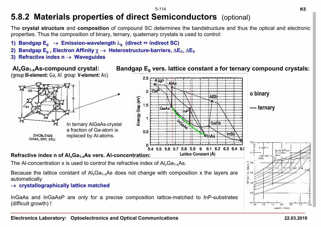
K5
______________________________________________________________________________________________________________________________
Electronics Laboratory: Optoelectronics and Optical Communications 22.03.2010
5-114
5.8.2 Materials properties of direct Semiconductors (optional)
The crystal structure and composition of compound SC determines the bandstructure and thus the optical and electronic properties. Thus the composition of binary, ternary, quaternary crystals is used to control:
1) Bandgap Eg → Emission-wavelength λg (direct indirect SC) 2) Bandgap Eg , Electron Affinity χ → Heterostructure-barriers, ΔEC, ΔEV 3) Refractive index n → Waveguides AlxGa1-xAs-compound crystal: Bandgap Eg vers. lattice constant a for ternary compound crystals: (group III-element: Ga, Al group V-element: As)
o binary ---- ternary
Refractive index n of AlxGa1-xAs vers. Al-concentration:
The Al-concentration x is used to control the refractive index of AlxGa1-xAs.
Because the lattice constant of AlxGa1-xAs does not change with composition x the layers are automatically → crystallographically lattice matched InGaAs and InGaAsP are only for a precise composition lattice-matched to InP-substrates (difficult growth) !
In ternary AlGaAs-crystal a fraction of Ga-atom is replaced by Al-atoms.