kelin j. kuhn - inteldownload.intel.com/pressroom/pdf/kkuhn/kuhn_ssdm_plenary_slides.pdf · kelin...
TRANSCRIPT
Kelin Kuhn / SSDM / Japan / 2009 1
Moore's Law past 32nm: Moore's Law past 32nm: Future Challenges in Device ScalingFuture Challenges in Device Scaling
Kelin J. KuhnKelin J. KuhnIntel FellowIntel Fellow
Director of Advanced Device Technology Director of Advanced Device Technology Intel CorporationIntel Corporation
Kelin Kuhn / SSDM / Japan / 2009 2
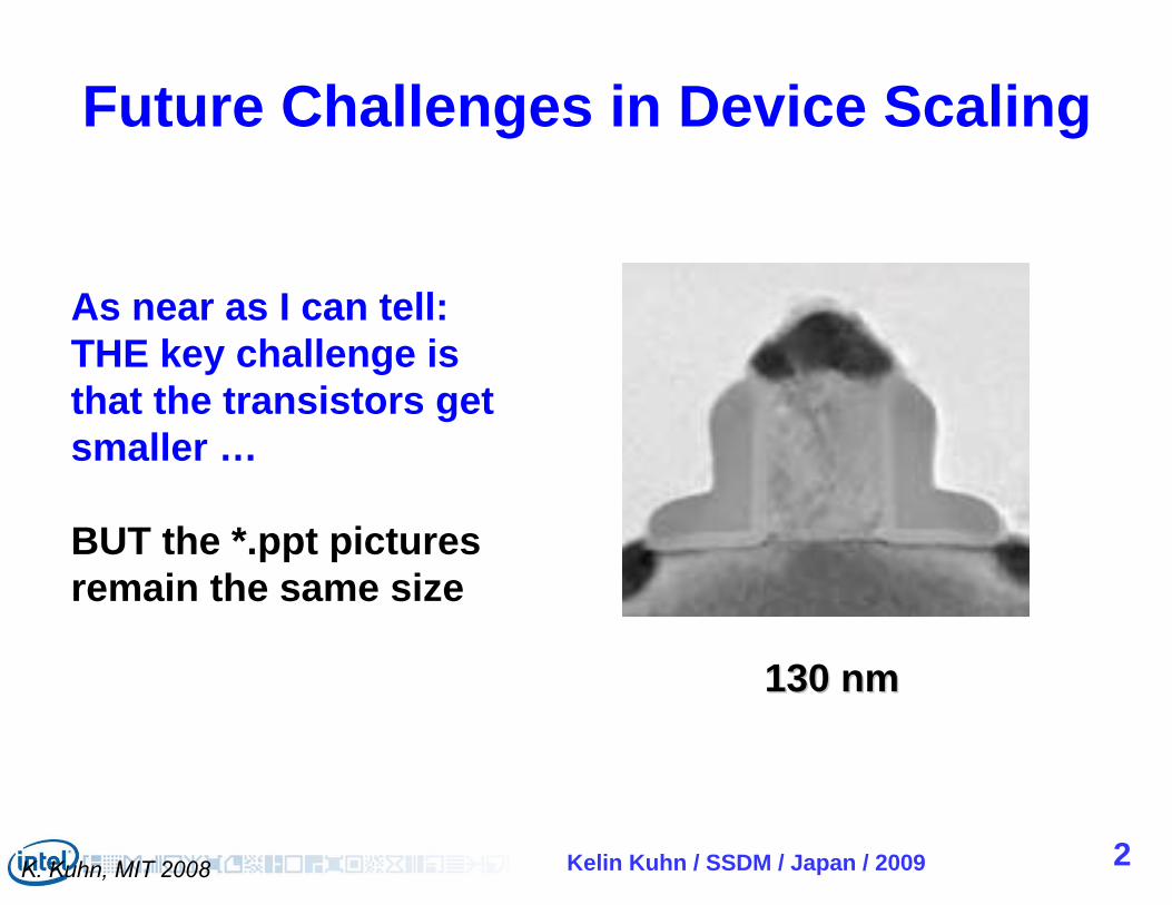
Future Challenges in Device Scaling
130 nm130 nm
As near as I can tell:THE key challenge is that the transistors get smaller …
BUT the *.ppt pictures remain the same size
K. Kuhn, MIT 2008
Kelin Kuhn / SSDM / Japan / 2009 3
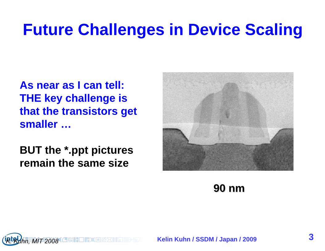
90 nm90 nm
K. Kuhn, MIT 2008
As near as I can tell:THE key challenge is that the transistors get smaller …
BUT the *.ppt pictures remain the same size
Future Challenges in Device Scaling
Kelin Kuhn / SSDM / Japan / 2009 4
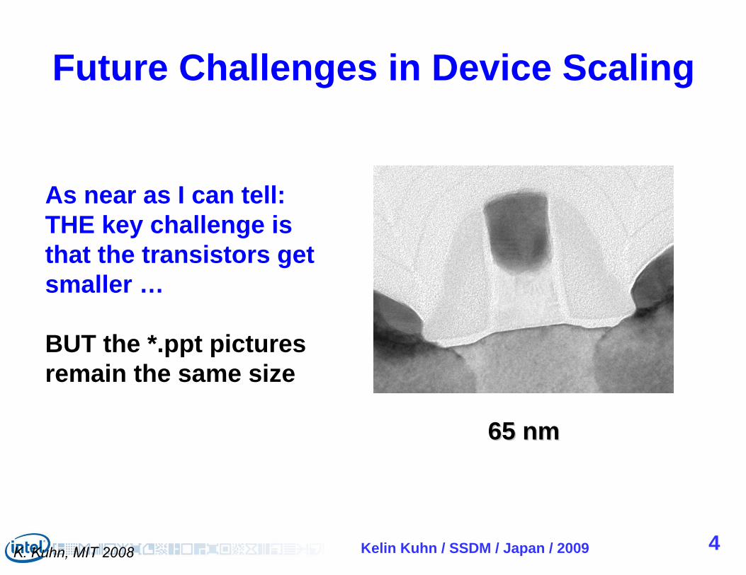
65 nm65 nm
K. Kuhn, MIT 2008
As near as I can tell:THE key challenge is that the transistors get smaller …
BUT the *.ppt pictures remain the same size
Future Challenges in Device Scaling
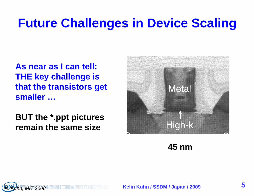
Kelin Kuhn / SSDM / Japan / 2009 5
45 nm45 nm
K. Kuhn, MIT 2008
As near as I can tell:THE key challenge is that the transistors get smaller …
BUT the *.ppt pictures remain the same size
Future Challenges in Device Scaling

Kelin Kuhn / SSDM / Japan / 2009 6
130 nm130 nm
K. Kuhn, MIT 2008
As near as I can tell:THE key challenge is that the transistors get smaller …
BUT the *.ppt pictures remain the same size
Maybe it would help if we SCALED THEM TOO!
Future Challenges in Device Scaling
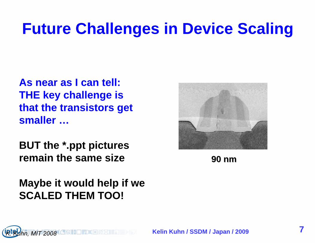
Kelin Kuhn / SSDM / Japan / 2009 7
90 nm90 nm
K. Kuhn, MIT 2008
As near as I can tell:THE key challenge is that the transistors get smaller …
BUT the *.ppt pictures remain the same size
Maybe it would help if we SCALED THEM TOO!
Future Challenges in Device Scaling
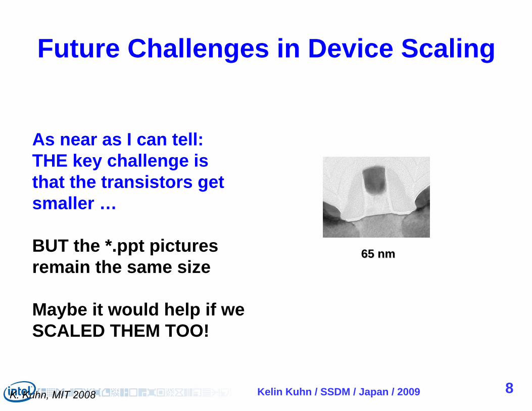
Kelin Kuhn / SSDM / Japan / 2009 8
65 nm65 nm
K. Kuhn, MIT 2008
As near as I can tell:THE key challenge is that the transistors get smaller …
BUT the *.ppt pictures remain the same size
Maybe it would help if we SCALED THEM TOO!
Future Challenges in Device Scaling
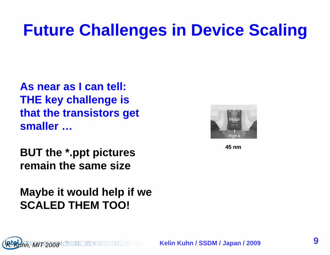
Kelin Kuhn / SSDM / Japan / 2009 9
45 nm45 nm
K. Kuhn, MIT 2008
As near as I can tell:THE key challenge is that the transistors get smaller …
BUT the *.ppt pictures remain the same size
Maybe it would help if we SCALED THEM TOO!
Future Challenges in Device Scaling
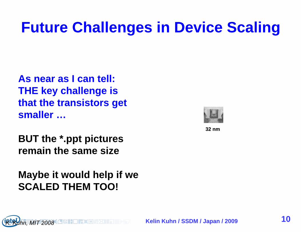
Kelin Kuhn / SSDM / Japan / 2009 10
32 nm32 nm
K. Kuhn, MIT 2008
As near as I can tell:THE key challenge is that the transistors get smaller …
BUT the *.ppt pictures remain the same size
Maybe it would help if we SCALED THEM TOO!
Future Challenges in Device Scaling
Kelin Kuhn / SSDM / Japan / 2009 11
AGENDA• Scaling history• Gate control
– High-k metal-gate– Structural enhancements
• Resistance• Capacitance• Mobility
– Strain– Orientation– Advanced channel materials
• Summary
Kelin Kuhn / SSDM / Japan / 2009 12
AGENDA• Scaling history• Gate control
– High-k metal-gate– Structural enhancements
• Resistance• Capacitance• Mobility
– Strain– Orientation– Advanced channel materials
• Summary
Kelin Kuhn / SSDM / Japan / 2009 13
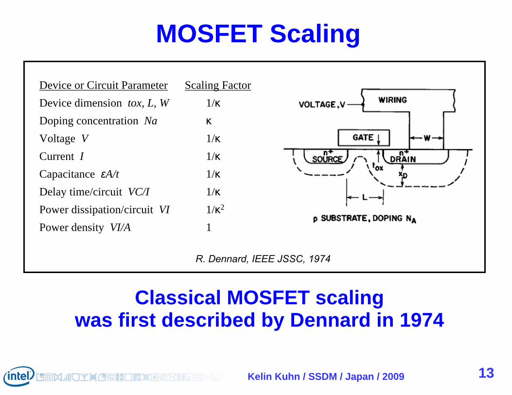
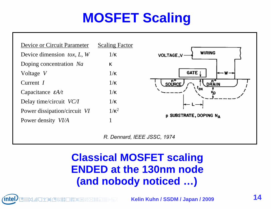
MOSFET Scaling
R. Dennard, IEEE JSSC, 1974
Device or Circuit Parameter Scaling FactorDevice dimension tox, L, W 1/κDoping concentration Na κVoltage V 1/κCurrent I 1/κCapacitance εA/t 1/κDelay time/circuit VC/I 1/κPower dissipation/circuit VI 1/κ2
Power density VI/A 1
Classical MOSFET scaling was first described by Dennard in 1974
Kelin Kuhn / SSDM / Japan / 2009 14
MOSFET Scaling
R. Dennard, IEEE JSSC, 1974
Device or Circuit Parameter Scaling FactorDevice dimension tox, L, W 1/κDoping concentration Na κVoltage V 1/κCurrent I 1/κCapacitance εA/t 1/κDelay time/circuit VC/I 1/κPower dissipation/circuit VI 1/κ2
Power density VI/A 1
Classical MOSFET scaling ENDED at the 130nm node (and nobody noticed …)
Kelin Kuhn / SSDM / Japan / 2009 15
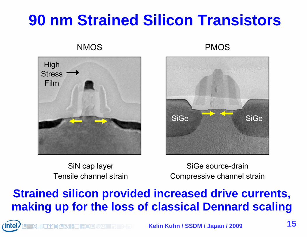
90 nm Strained Silicon Transistors
HighStressFilm
NMOS
SiGe SiGe
PMOS
SiN cap layer SiGe source-drainTensile channel strain Compressive channel strain
Strained silicon provided increased drive currents, making up for the loss of classical Dennard scaling
Kelin Kuhn / SSDM / Japan / 2009 16
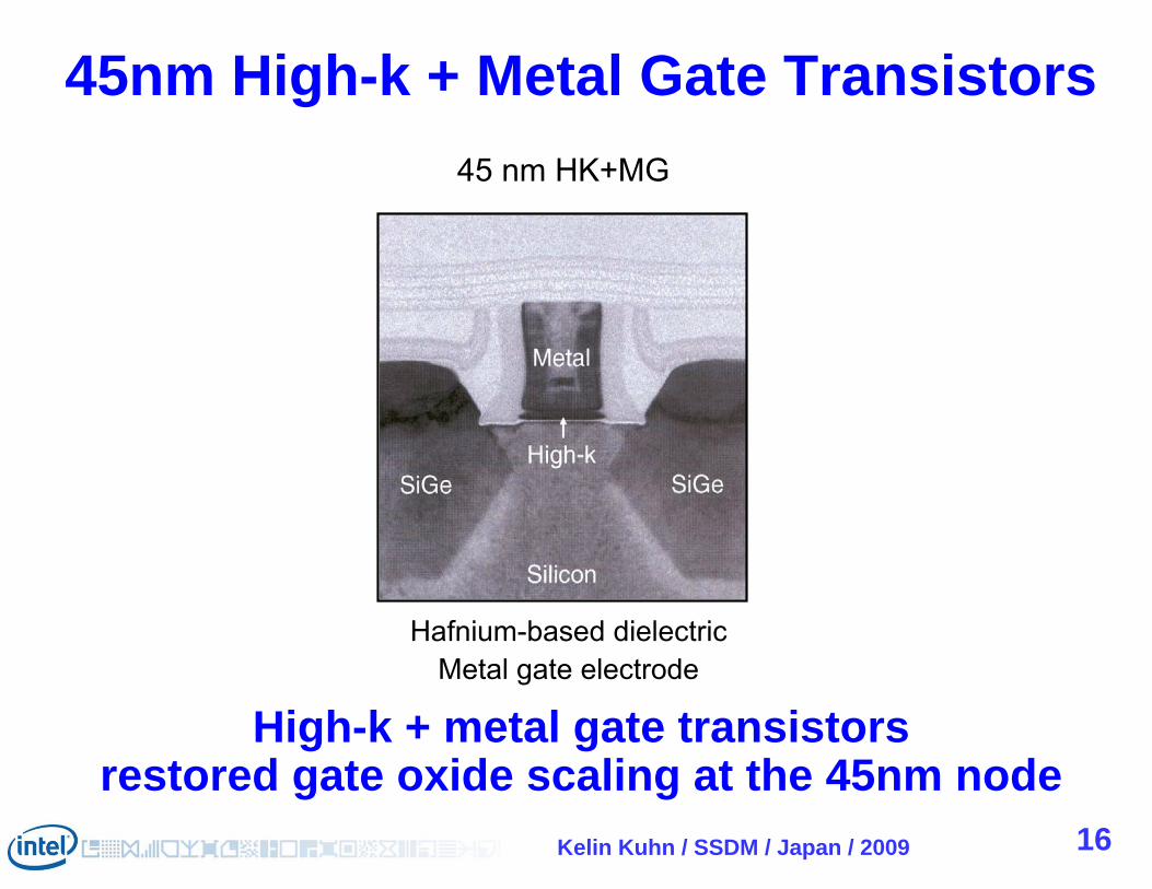
45nm High-k + Metal Gate Transistors45 nm HK+MG
High-k + metal gate transistors restored gate oxide scaling at the 45nm node
Hafnium-based dielectricMetal gate electrode
Kelin Kuhn / SSDM / Japan / 2009 17
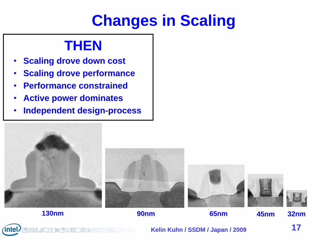
Changes in ScalingTHEN
• Scaling drove down cost• Scaling drove performance• Performance constrained• Active power dominates• Independent design-process
130nm 90nm 65nm 45nm 32nm
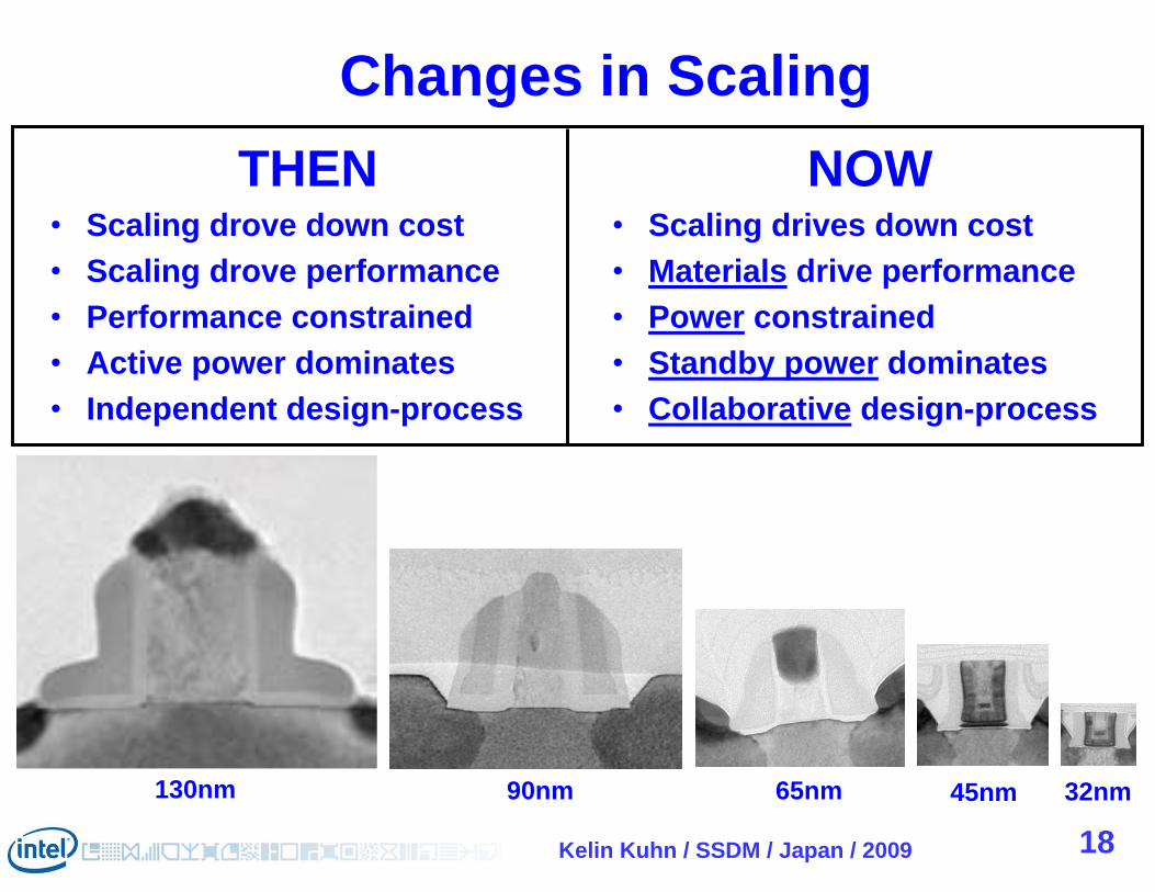
Kelin Kuhn / SSDM / Japan / 2009 18
Changes in ScalingTHEN
• Scaling drove down cost• Scaling drove performance• Performance constrained• Active power dominates• Independent design-process
NOW• Scaling drives down cost• Materials drive performance• Power constrained• Standby power dominates• Collaborative design-process
130nm 90nm 65nm 45nm 32nm
Kelin Kuhn / SSDM / Japan / 2009 19
0.1
1
10
100
1000
1960 1980 2000 2020YEAR
MIP
S/w
att
110100100010000100000
Mile
s pe
r gal
lon
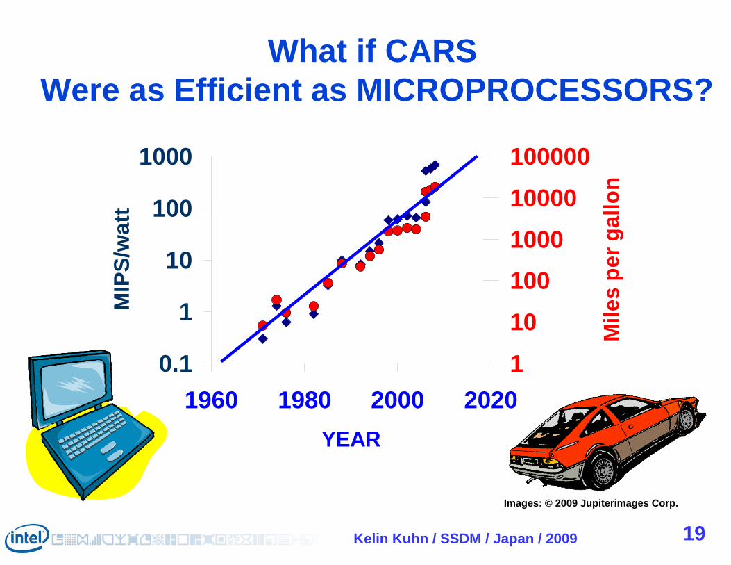
What if CARS Were as Efficient as MICROPROCESSORS?
Images: © 2009 Jupiterimages Corp.
Kelin Kuhn / SSDM / Japan / 2009 20
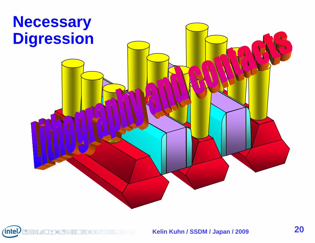
NecessaryDigression
Kelin Kuhn / SSDM / Japan / 2009 21
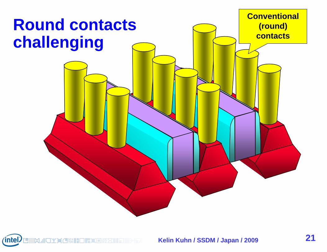
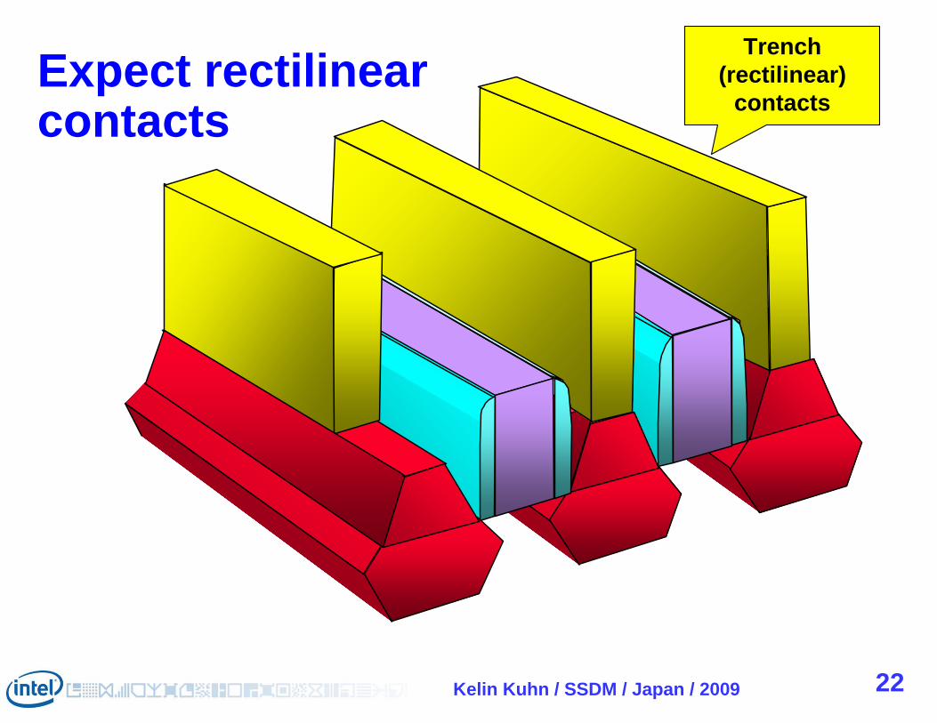
Conventional (round)
contactsRound contacts challenging
Kelin Kuhn / SSDM / Japan / 2009 22
Trench (rectilinear)
contactsExpect rectilinearcontacts

Kelin Kuhn / SSDM / Japan / 2009 23
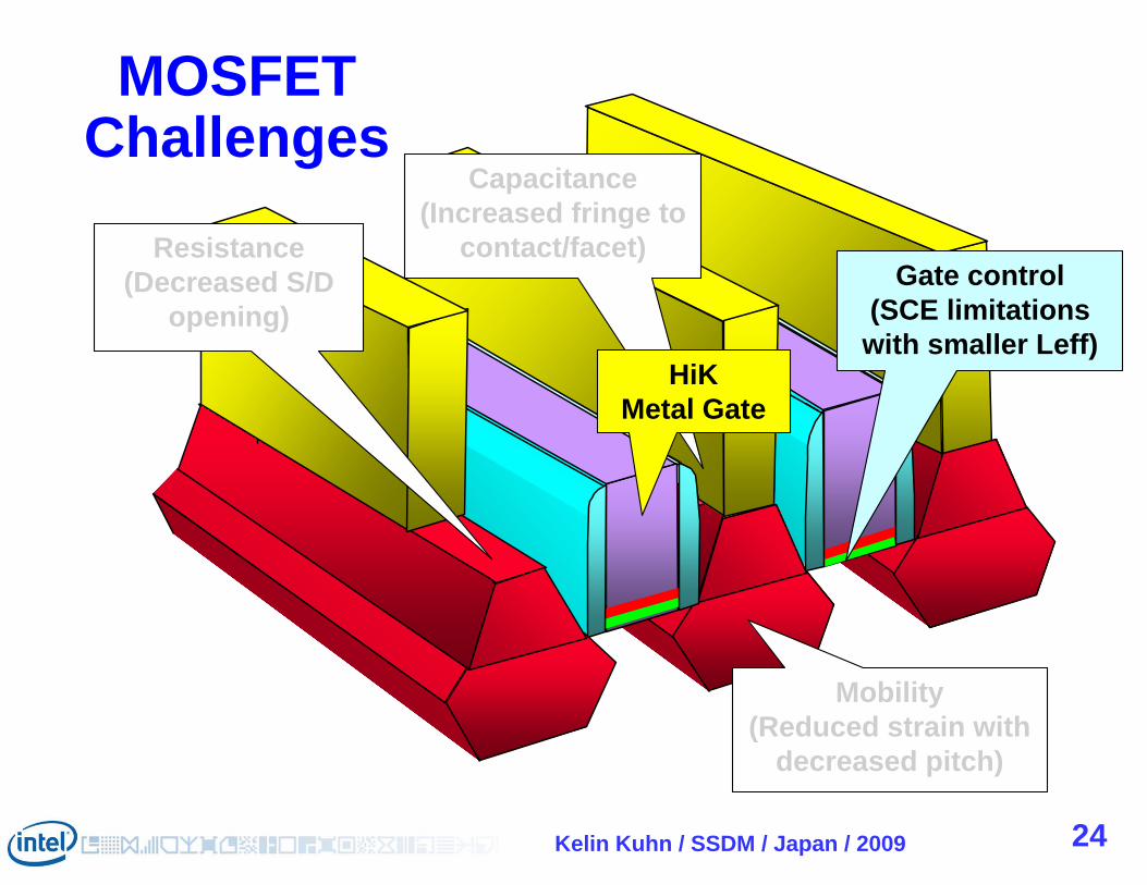
MOSFET Challenges
Mobility(Reduced strain with
decreased pitch)
Gate control(SCE limitations
with smaller Leff)
Capacitance (Increased fringe to
contact/facet)Resistance(Decreased S/D
opening)
Kelin Kuhn / SSDM / Japan / 2009 24
Mobility(Reduced strain with
decreased pitch)
MOSFET Challenges
Capacitance (Increased fringe to
contact/facet)Resistance(Decreased S/D
opening)
HiKMetal Gate
Gate control(SCE limitations
with smaller Leff)
Kelin Kuhn / SSDM / Japan / 2009 25
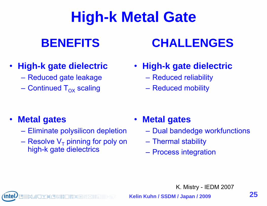
• High-k gate dielectric – Reduced gate leakage– Continued TOX scaling
• High-k gate dielectric – Reduced reliability– Reduced mobility
• Metal gates– Eliminate polysilicon depletion– Resolve VT pinning for poly on
high-k gate dielectrics
• Metal gates– Dual bandedge workfunctions– Thermal stability– Process integration
BENEFITS CHALLENGES
High-k Metal Gate
K. Mistry - IEDM 2007
Kelin Kuhn / SSDM / Japan / 2009 26
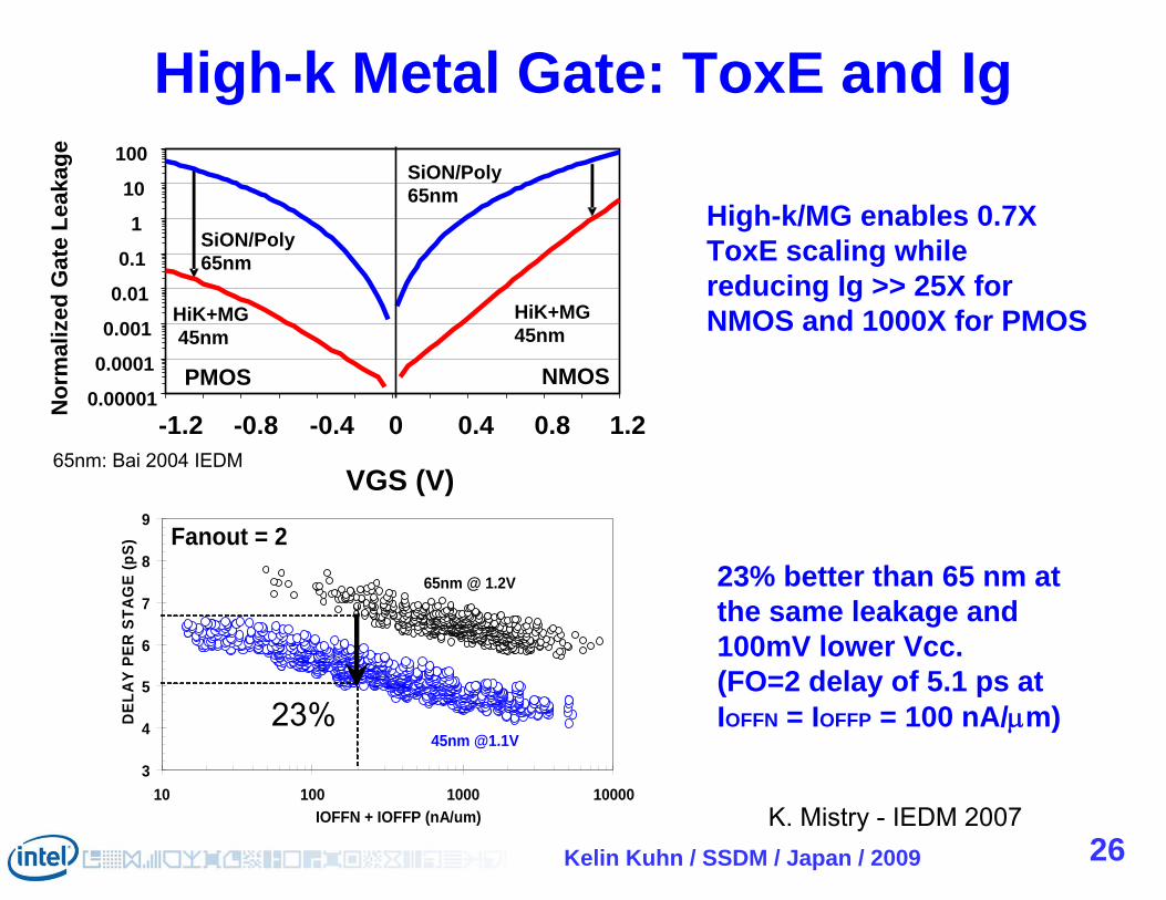
High-k/MG enables 0.7X ToxE scaling while reducing Ig >> 25X for NMOS and 1000X for PMOS
65nm: Bai 2004 IEDM
0.00001
0.0001
0.001
0.01
0.1
1
10
100
-1.2 -0.8 -0.4 0 0.4 0.8 1.2
VGS (V)
Nor
mal
ized
Gat
e Le
akag
e
SiON/Poly 65nm
HiK+MG45nm
NMOS PMOS
HiK+MG45nm
SiON/Poly 65nm
K. Mistry - IEDM 2007
High-k Metal Gate: ToxE and Ig
Fanout = 2
3
4
5
6
7
8
9
10 100 1000 10000IOFFN + IOFFP (nA/um)
DEL
AY
PER
STA
GE
(pS)
65nm @ 1.2V
45nm @1.1V
23% better than 65 nm at the same leakage and 100mV lower Vcc. (FO=2 delay of 5.1 ps at IOFFN = IOFFP = 100 nA/m)23%
Kelin Kuhn / SSDM / Japan / 2009 27
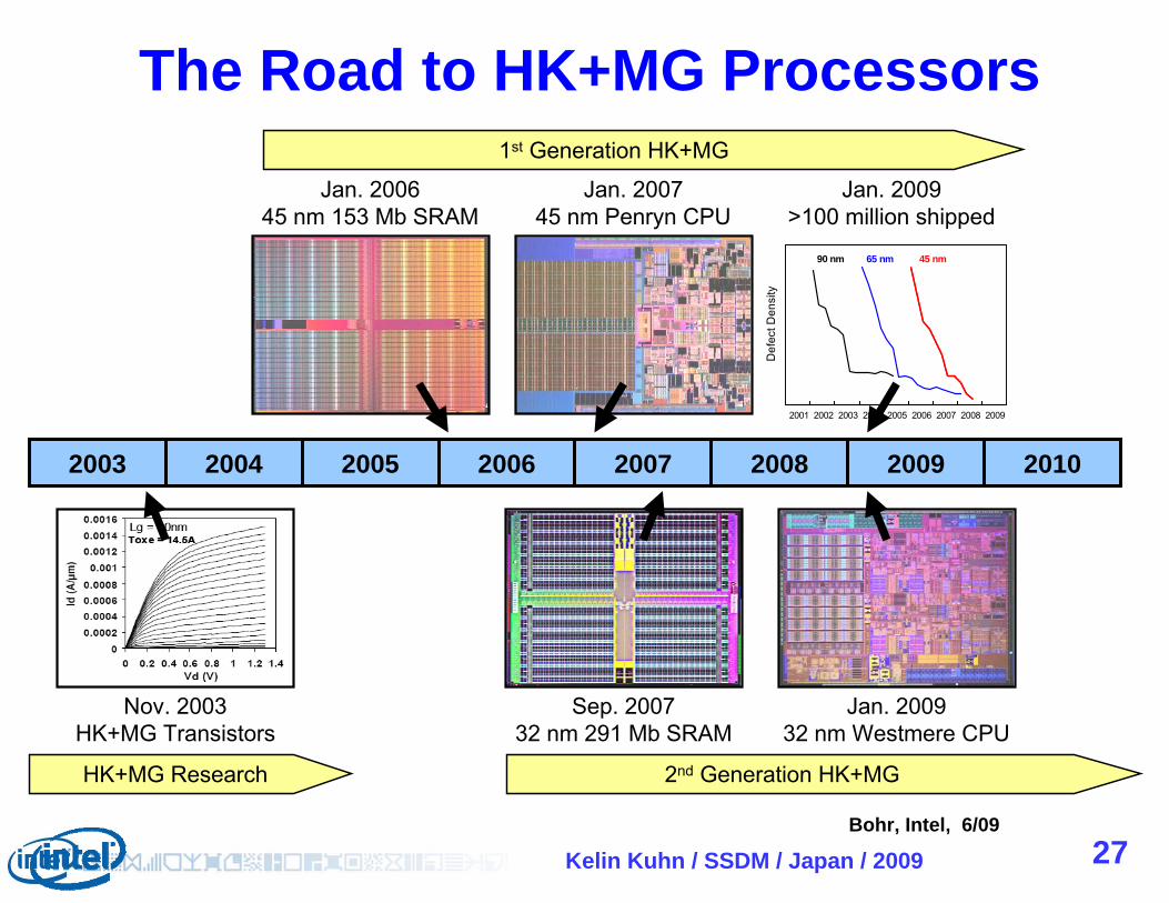
The Road to HK+MG Processors
Bohr, Intel, 6/09
20042003
Nov. 2003HK+MG Transistors
HK+MG Research
20062005
Jan. 200645 nm 153 Mb SRAM
1st Generation HK+MG
2007
2nd Generation HK+MG
Sep. 200732 nm 291 Mb SRAM
Jan. 200745 nm Penryn CPU
2008 2009 2010
Jan. 200932 nm Westmere CPU
90 nm 65 nm 45 nm
2001 2002 2003 2004 2005 2006 2007 2008 2009
Def
ect D
ensi
ty
Jan. 2009>100 million shipped
Kelin Kuhn / SSDM / Japan / 2009
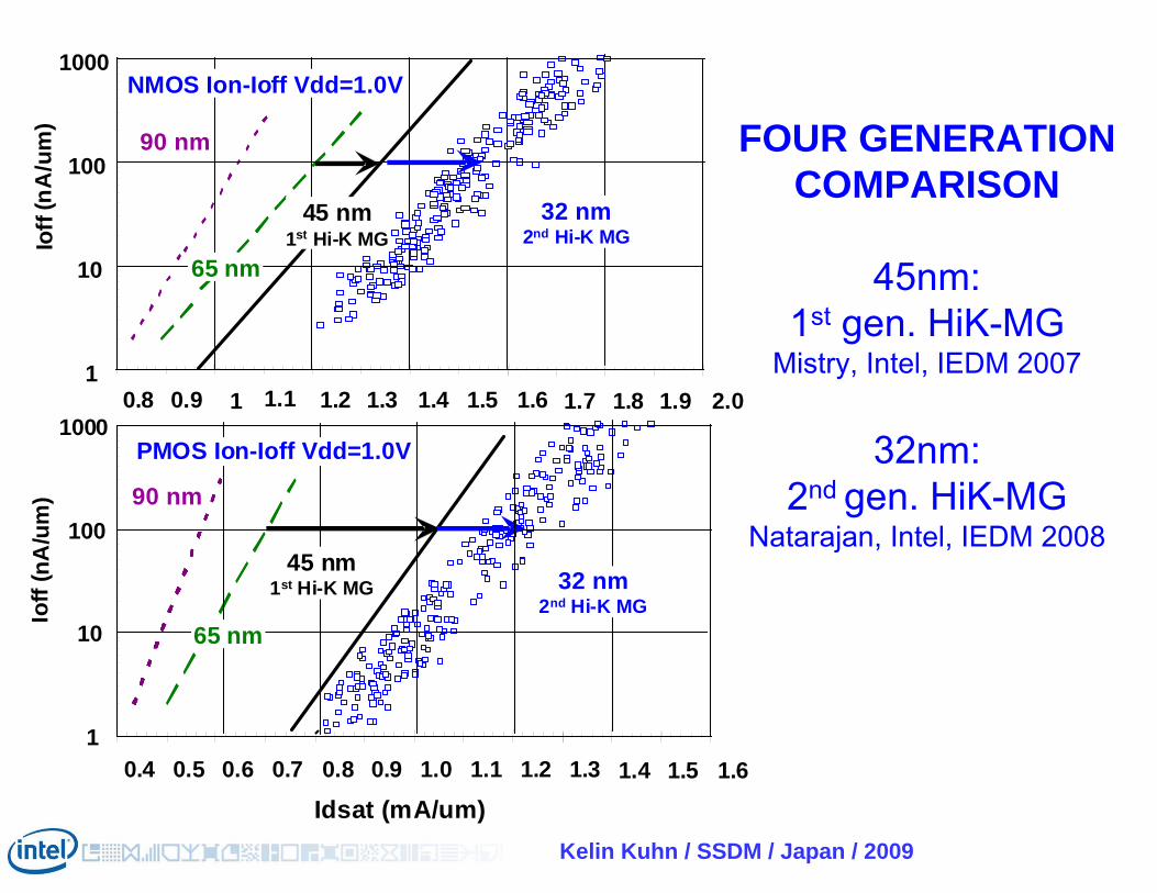
FOUR GENERATION COMPARISON
45nm: 1st gen. HiK-MG
Mistry, Intel, IEDM 2007
32nm:2nd gen. HiK-MG
Natarajan, Intel, IEDM 2008
1
10
100
1000
0.4 0.5 0.6 0.7 0.8 0.9 1.0 1.1 1.2 1.3
90 nm
1.4 1.5 1.6
1 1.2 1.4 1.61
10
100
1000
0.8 0.9 1.1 1.3 1.5 1.8 2.01.7 1.9
65 nm
90 nm
NMOS Ion-Ioff Vdd=1.0V
Idsat (mA/um)
Ioff
(nA
/um
)Io
ff( n
A/u
m)
45 nm1st Hi-K MG
PMOS Ion-Ioff Vdd=1.0V
65 nm
32 nm2nd Hi-K MG
45 nm1st Hi-K MG
32 nm2nd Hi-K MG
Kelin Kuhn / SSDM / Japan / 2009 29
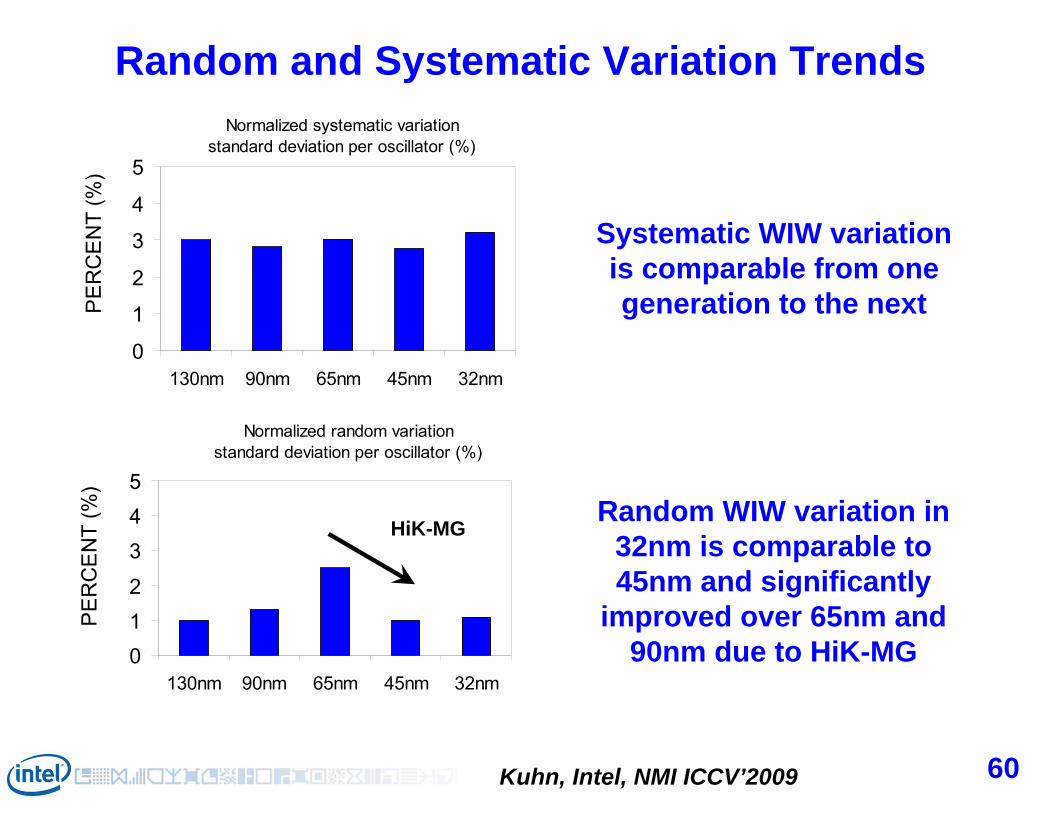
Normalized random variationstandard deviation per oscillator (%)
012
345
130nm 90nm 65nm 45nm 32nm
PE
RC
EN
T (%
) Normalized systematic variation
standard deviation per oscillator (%)
0
1
2
3
4
5
130nm 90nm 65nm 45nm 32nm
PE
RC
EN
T (%
) Random and Systematic Variation Trends
Systematic WIW variation is comparable from one generation to the next
Random WIW variation in 32nm is comparable to 45nm and significantly
improved over 65nm and 90nm due to HiK-MG
HiK-MG
60 Kuhn, Intel, NMI ICCV’2009

Kelin Kuhn / SSDM / Japan / 2009 30
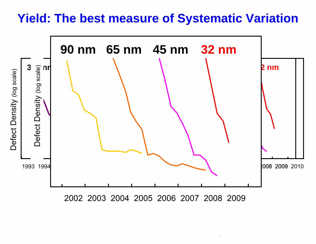
90 nm 65 nm 45 nm 32 nm
2002 2003 2004 2005 2006 2007 2008 2009 20101993 1994 1995 1996 1997 1998 1999 2000 2001
350 nm 250 nm 180 nm 130 nm
Def
ect D
ensi
ty (l
og s
cale
)Yield: The best measure of Systematic Variation
Kelin Kuhn / SSDM / Japan / 2009 31
90 nm 65 nm 45 nm 32 nm
2002 2003 2004 2005 2006 2007 2008 2009 20101993 1994 1995 1996 1997 1998 1999 2000 2001
350 nm 250 nm 180 nm 130 nm
Def
ect D
ensi
ty (l
og s
cale
) 90 nm 65 nm 45 nm 32 nm
2002 2003 2004 2005 2006 2007 2008 2009
Def
ect D
ensi
ty (l
og s
cale
)
2002 2003 2004 2005 2006 2007 2008 2009
90 nm 65 nm 45 nm 32 nm
Yield: The best measure of Systematic Variation
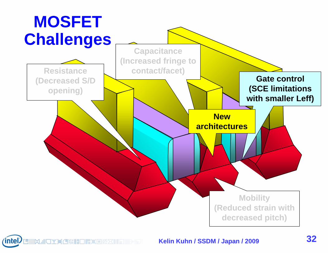
Kelin Kuhn / SSDM / Japan / 2009 32
Mobility(Reduced strain with
decreased pitch)
Resistance(Decreased S/D
opening)
Capacitance (Increased fringe to
contact/facet)
MOSFET Challenges
Gate control(SCE limitations
with smaller Leff)
New architectures

33Kelin Kuhn / SSDM / Japan / 2009
Ultra-thinbody (UTB)
Ultra-thin bodywith RSD
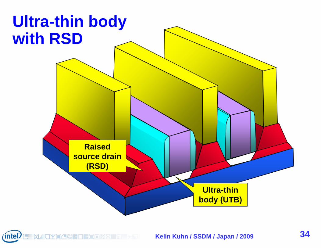
34Kelin Kuhn / SSDM / Japan / 2009
Ultra-thinbody (UTB)
Ultra-thin bodywith RSD
Raised source drain
(RSD)
35Kelin Kuhn / SSDM / Japan / 2009
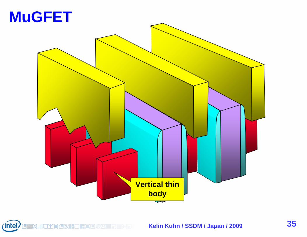
MuGFET
Vertical thin body
36Kelin Kuhn / SSDM / Japan / 2009
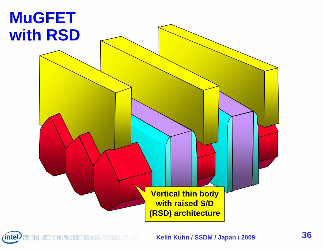
Vertical thin body with raised S/D
(RSD) architecture
MuGFETwith RSD
37Kelin Kuhn / SSDM / Japan / 2009
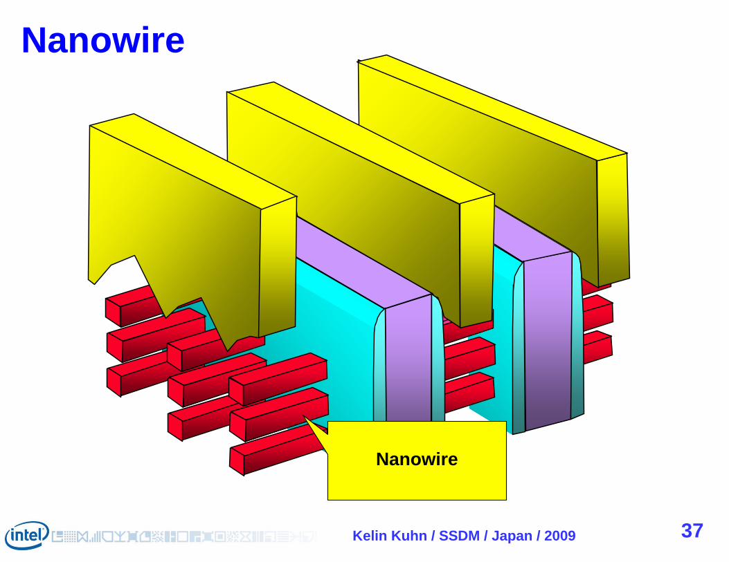
Nanowire
Nanowire

38Kelin Kuhn / SSDM / Japan / 2009
Nanowirewith RSD
Nanowirewith raised S/D
(RSD) architecture

39Kelin Kuhn / SSDM / Japan / 2009
Nanowirewith RSD
Nanowirewith raised S/D
(RSD) architecture
Looking at all these in more detail
40Kelin Kuhn / SSDM / Japan / 2009
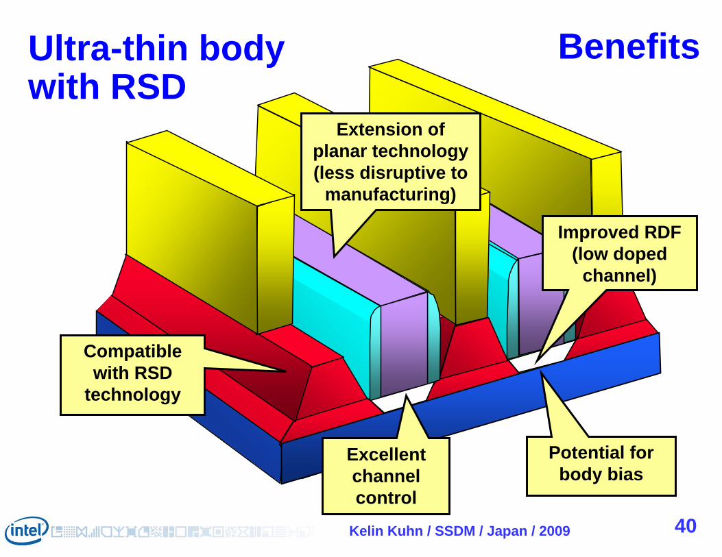
Ultra-thin bodywith RSD
Benefits
Compatible with RSD
technology
Extension of planar technology(less disruptive to
manufacturing)
Excellent channel control
Improved RDF (low doped
channel)
Potential for body bias
41Kelin Kuhn / SSDM / Japan / 2009
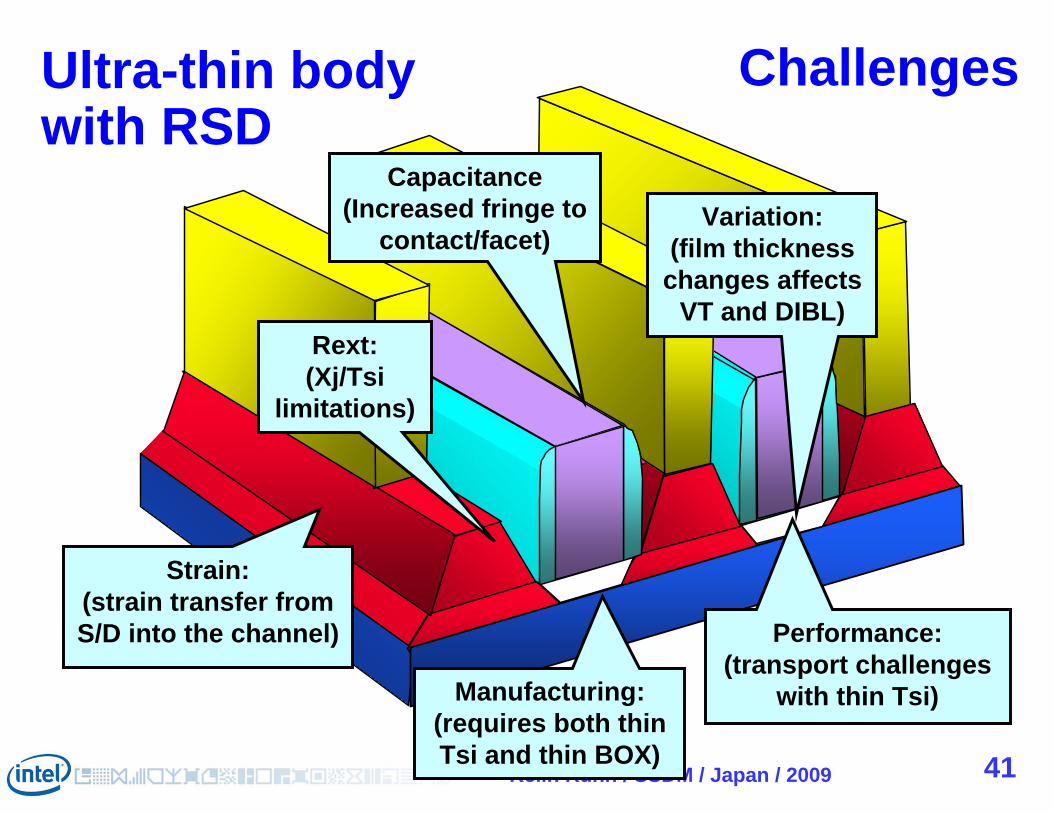
Rext: (Xj/Tsi
limitations)
Manufacturing:(requires both thin Tsi and thin BOX)
Strain:(strain transfer from S/D into the channel) Performance:
(transport challenges with thin Tsi)
Variation:(film thickness
changes affects VT and DIBL)
ChallengesUltra-thin bodywith RSD
Capacitance (Increased fringe to
contact/facet)
42Kelin Kuhn / SSDM / Japan / 2009
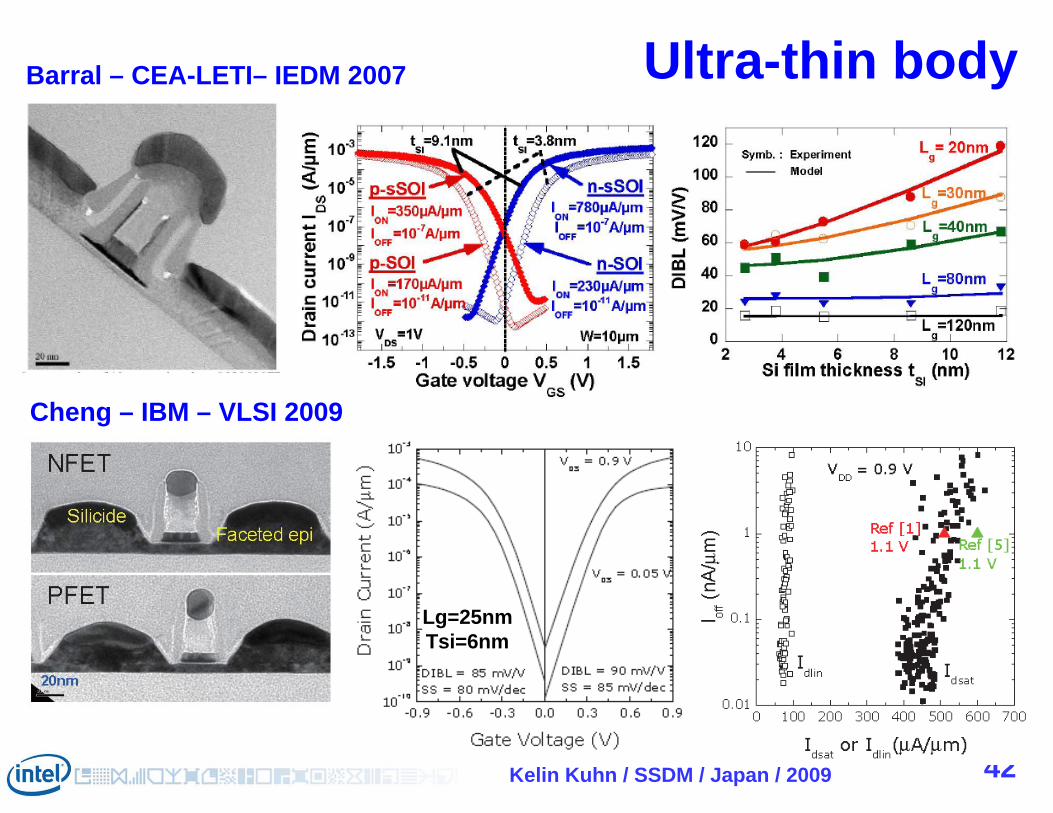
Ultra-thin body
Lg=25nmTsi=6nm
Barral – CEA-LETI– IEDM 2007
Cheng – IBM – VLSI 2009
43Kelin Kuhn / SSDM / Japan / 2009
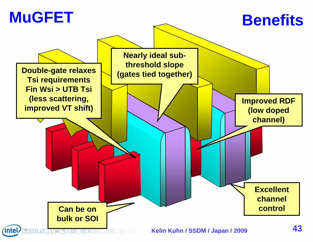
MuGFET Benefits
Double-gate relaxes Tsi requirementsFin Wsi > UTB Tsi(less scattering,
improved VT shift)
Excellent channel control
Improved RDF (low doped
channel)
Nearly ideal sub-threshold slope
(gates tied together)
Can be on bulk or SOI
44Kelin Kuhn / SSDM / Japan / 2009
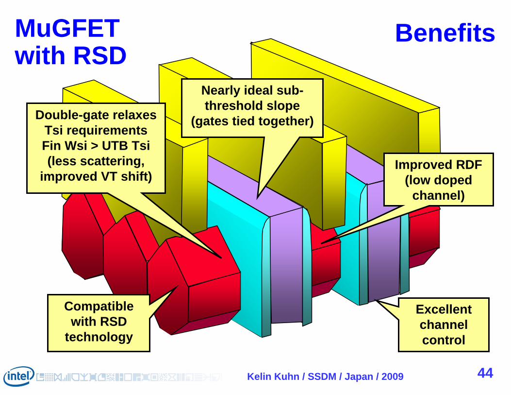
MuGFETwith RSD
Compatible with RSD
technology
Double-gate relaxes Tsi requirementsFin Wsi > UTB Tsi(less scattering,
improved VT shift)
Excellent channel control
Improved RDF (low doped
channel)
Benefits
Nearly ideal sub-threshold slope
(gates tied together)
45Kelin Kuhn / SSDM / Japan / 2009
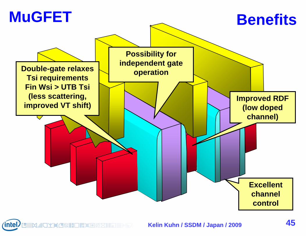
MuGFET Benefits
Double-gate relaxes Tsi requirementsFin Wsi > UTB Tsi(less scattering,
improved VT shift)
Excellent channel control
Improved RDF (low doped
channel)
Possibility for independent gate
operation
46Kelin Kuhn / SSDM / Japan / 2009
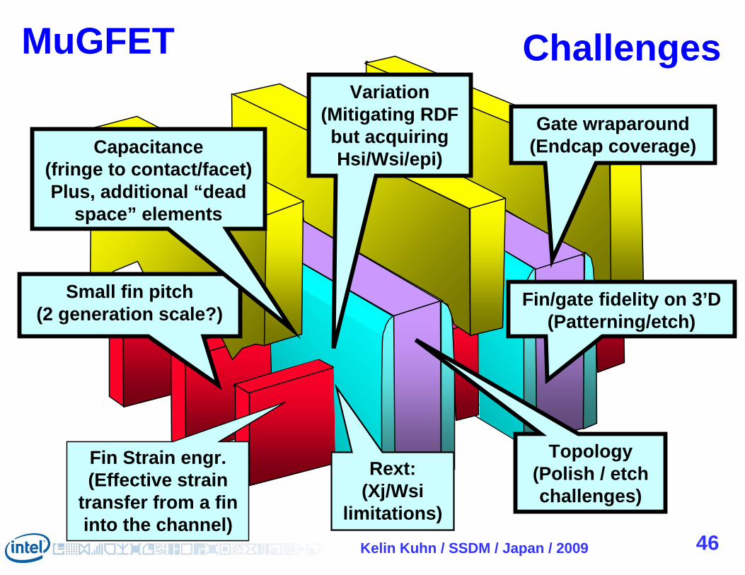
MuGFET
Rext: (Xj/Wsi
limitations)
Small fin pitch (2 generation scale?)
Fin/gate fidelity on 3’D(Patterning/etch)
Topology(Polish / etch challenges)
Fin Strain engr.(Effective strain
transfer from a fin into the channel)
Variation(Mitigating RDF but acquiring Hsi/Wsi/epi)
Gate wraparound(Endcap coverage)
Challenges
Capacitance (fringe to contact/facet)Plus, additional “dead
space” elements
Kelin Kuhn / SSDM / Japan / 2009 47
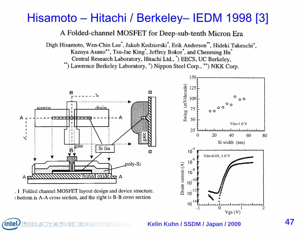
Hisamoto – Hitachi / Berkeley– IEDM 1998 [3]
48Kelin Kuhn / SSDM / Japan / 2009
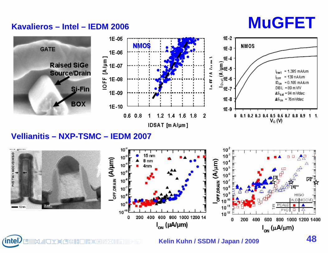
MuGFETKavalieros – Intel – IEDM 2006
Vellianitis – NXP-TSMC – IEDM 2007
49Kelin Kuhn / SSDM / Japan / 2009
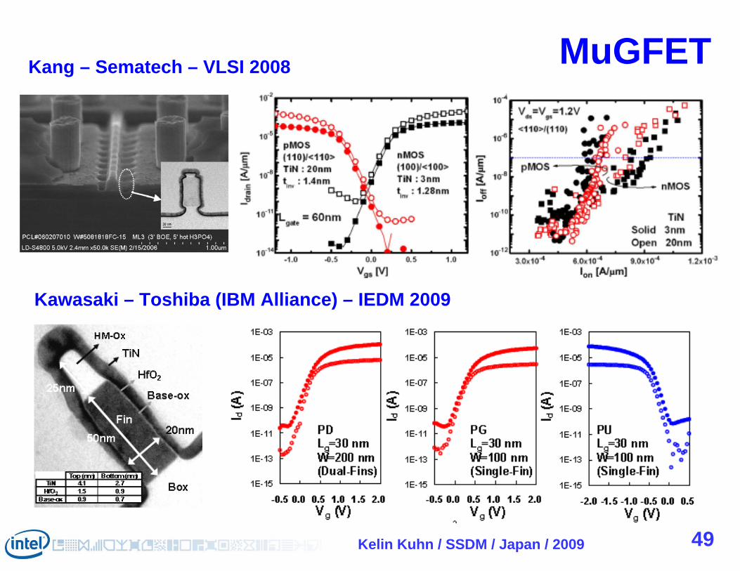
Kawasaki – Toshiba (IBM Alliance) – IEDM 2009
Kang – Sematech – VLSI 2008 MuGFET
50Kelin Kuhn / SSDM / Japan / 2009
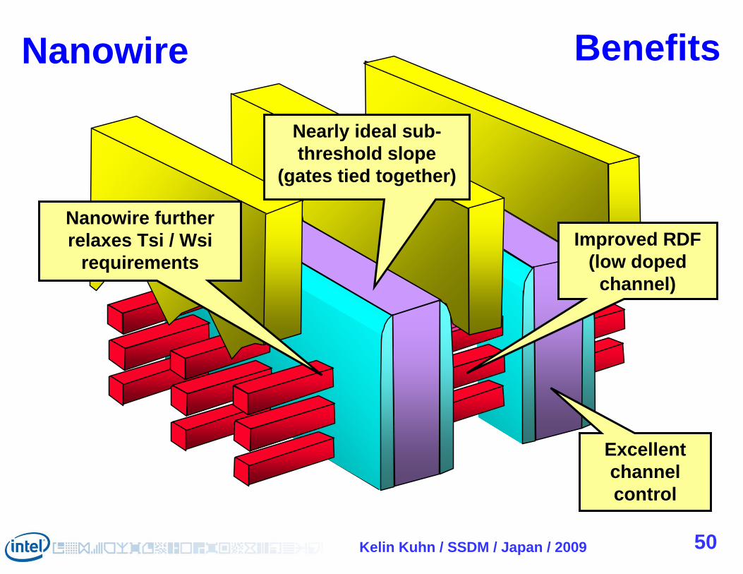
Nanowire further relaxes Tsi / Wsi
requirements
Excellent channel control
Improved RDF (low doped
channel)
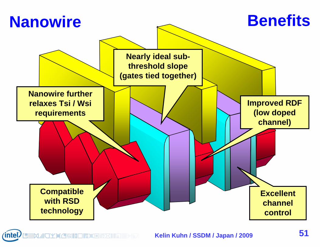
Nanowire Benefits
Nearly ideal sub-threshold slope
(gates tied together)
51Kelin Kuhn / SSDM / Japan / 2009
BenefitsNanowire
Compatible with RSD
technology
Nanowire further relaxes Tsi / Wsi
requirements
Excellent channel control
Improved RDF (low doped
channel)
Nearly ideal sub-threshold slope
(gates tied together)

52Kelin Kuhn / SSDM / Japan / 2009
Nanowire further relaxes Tsi / Wsi
requirements
Excellent channel control
Improved RDF (low doped
channel)
Possibility for independent gate
operation
Nanowire Benefits
53Kelin Kuhn / SSDM / Japan / 2009
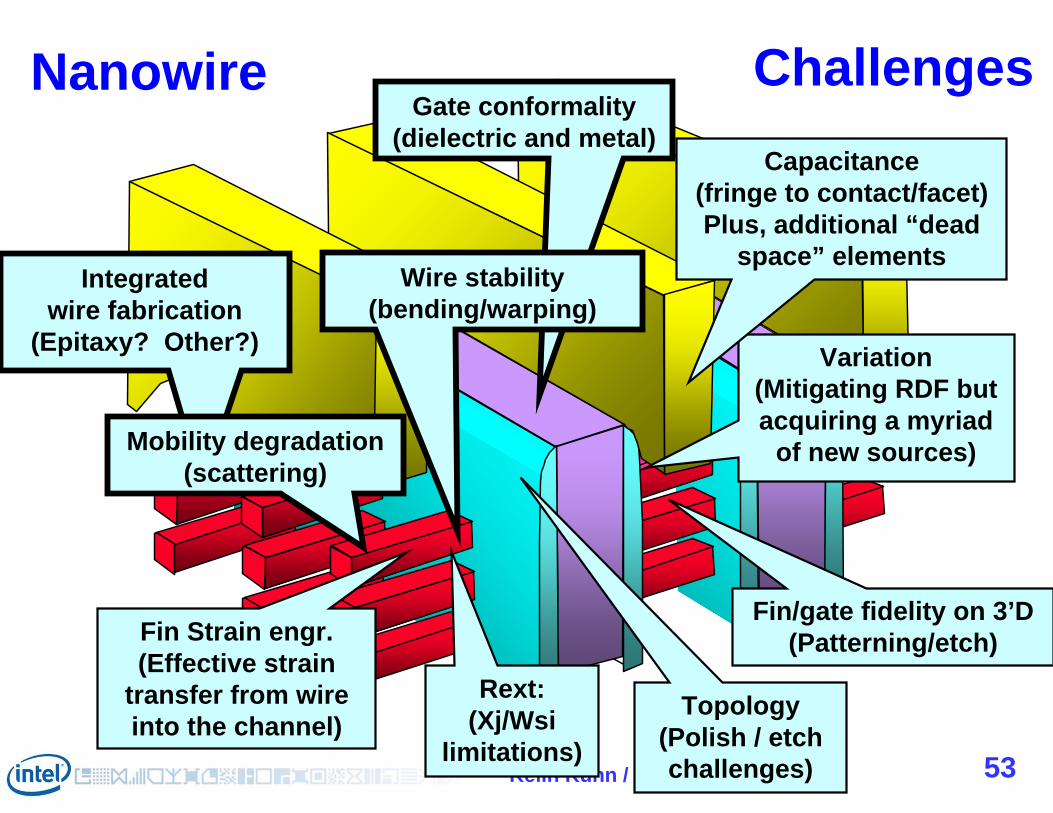
Rext: (Xj/Wsi
limitations)
Fin Strain engr.(Effective strain
transfer from wire into the channel)
Variation(Mitigating RDF but acquiring a myriad
of new sources)
Nanowire Challenges
Fin/gate fidelity on 3’D(Patterning/etch)
Topology(Polish / etch challenges)
Capacitance (fringe to contact/facet)Plus, additional “dead
space” elementsIntegrated
wire fabrication (Epitaxy? Other?)
Gate conformality(dielectric and metal)
Wire stability(bending/warping)
Mobility degradation(scattering)
54Kelin Kuhn / SSDM / Japan / 2009
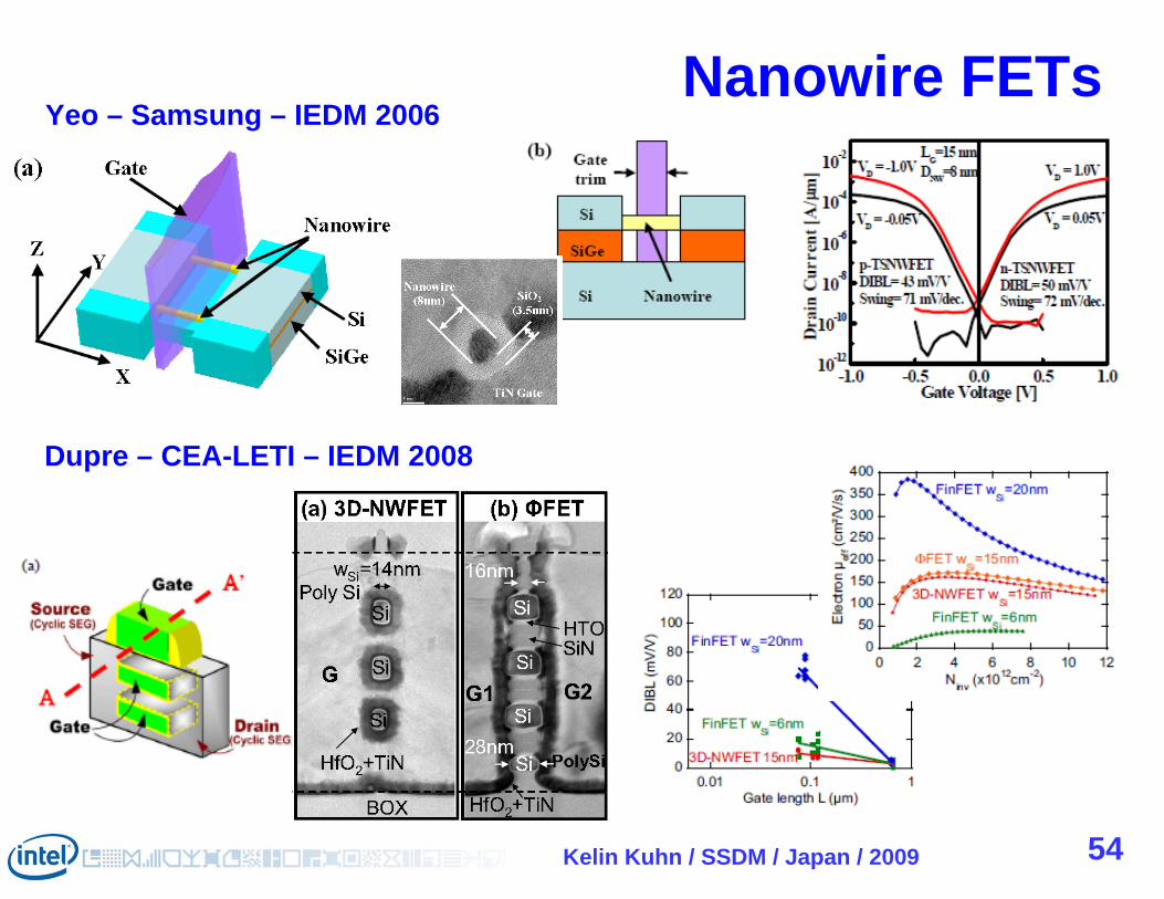
Nanowire FETsYeo – Samsung – IEDM 2006
Dupre – CEA-LETI – IEDM 2008
Kelin Kuhn / SSDM / Japan / 2009 55
AGENDA• Scaling history• Gate control
– High-k metal-gate– Structural enhancements
• Resistance• Capacitance• Mobility
– Strain– Orientation– Advanced channel materials
• Summary
56Kelin Kuhn / SSDM / Japan / 2009
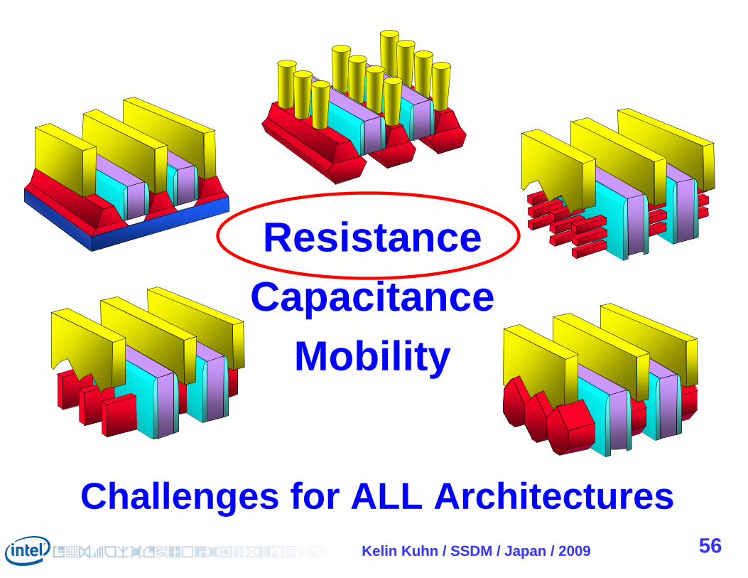
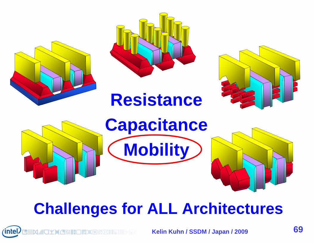
Challenges for ALL Architectures
ResistanceCapacitance
Mobility
Kelin Kuhn / SSDM / Japan / 2009 57
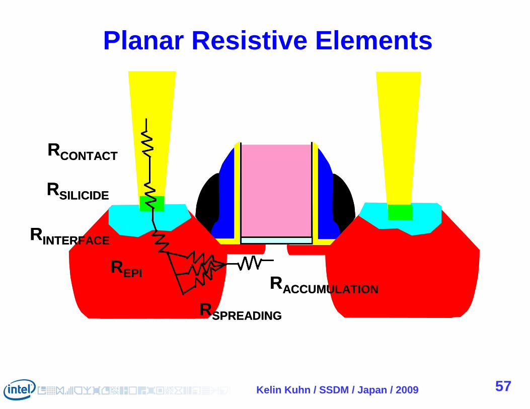
Planar Resistive Elements
RACCUMULATION
RSPREADING
REPI
RCONTACT
RINTERFACE
RSILICIDE
RACCUMULATION
RSPREADING
REPI
RCONTACT
RINTERFACE
RSILICIDE
Kelin Kuhn / SSDM / Japan / 2009 58
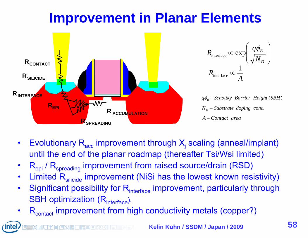
Improvement in Planar Elements
.concdopingSubstrateND
)(SBHHeightBarrierSchottkyq B
• Evolutionary Racc improvement through Xj scaling (anneal/implant) until the end of the planar roadmap (thereafter Tsi/Wsi limited)
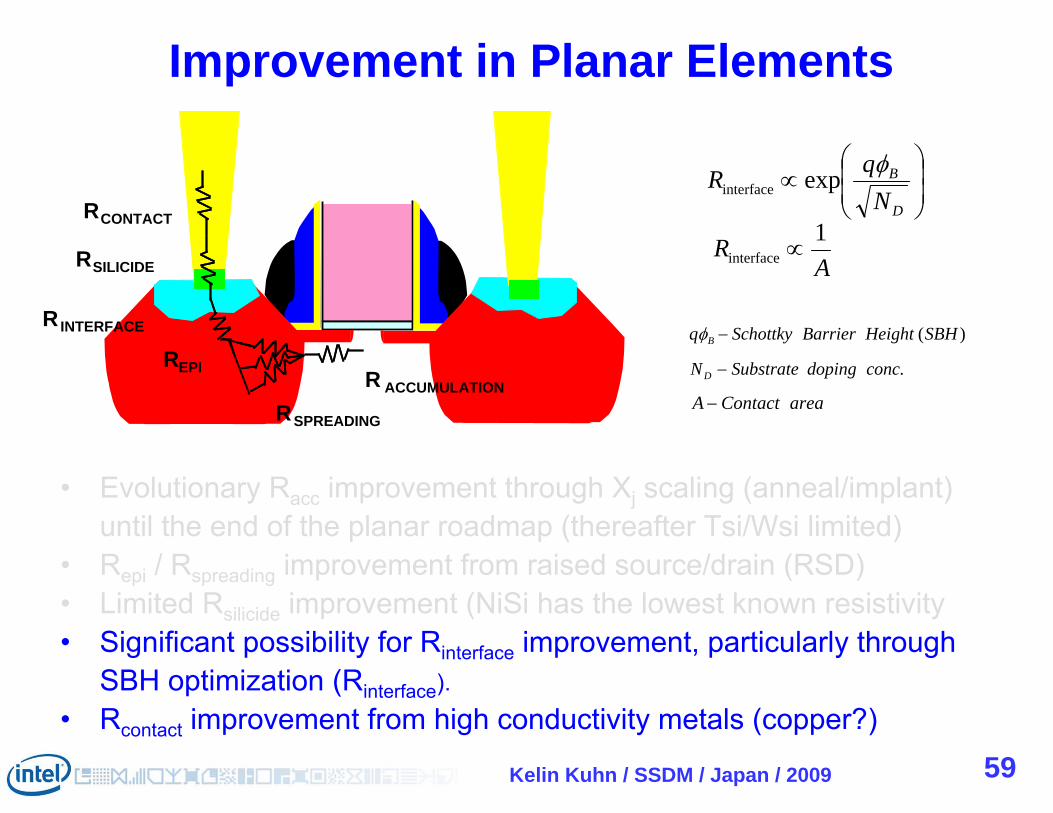
• Repi / Rspreading improvement from raised source/drain (RSD)• Limited Rsilicide improvement (NiSi has the lowest known resistivity)• Significant possibility for Rinterface improvement, particularly through
SBH optimization (Rinterface).• Rcontact improvement from high conductivity metals (copper?)
D
B
NqR expinterface
AR 1
interface
areaContactA R ACCUMULATION
RSPREADING
REPI
RCONTACT
RINTERFACE
RSILICIDE
Kelin Kuhn / SSDM / Japan / 2009 59
Improvement in Planar Elements
.concdopingSubstrateND
)(SBHHeightBarrierSchottkyq B
• Evolutionary Racc improvement through Xj scaling (anneal/implant) until the end of the planar roadmap (thereafter Tsi/Wsi limited)
• Repi / Rspreading improvement from raised source/drain (RSD)• Limited Rsilicide improvement (NiSi has the lowest known resistivity)• Significant possibility for Rinterface improvement, particularly through
SBH optimization (Rinterface).• Rcontact improvement from high conductivity metals (copper?)
D
B
NqR expinterface
AR 1
interface
areaContactA R ACCUMULATION
RSPREADING
REPI
RCONTACT
RINTERFACE
RSILICIDE
Kelin Kuhn / SSDM / Japan / 2009 60
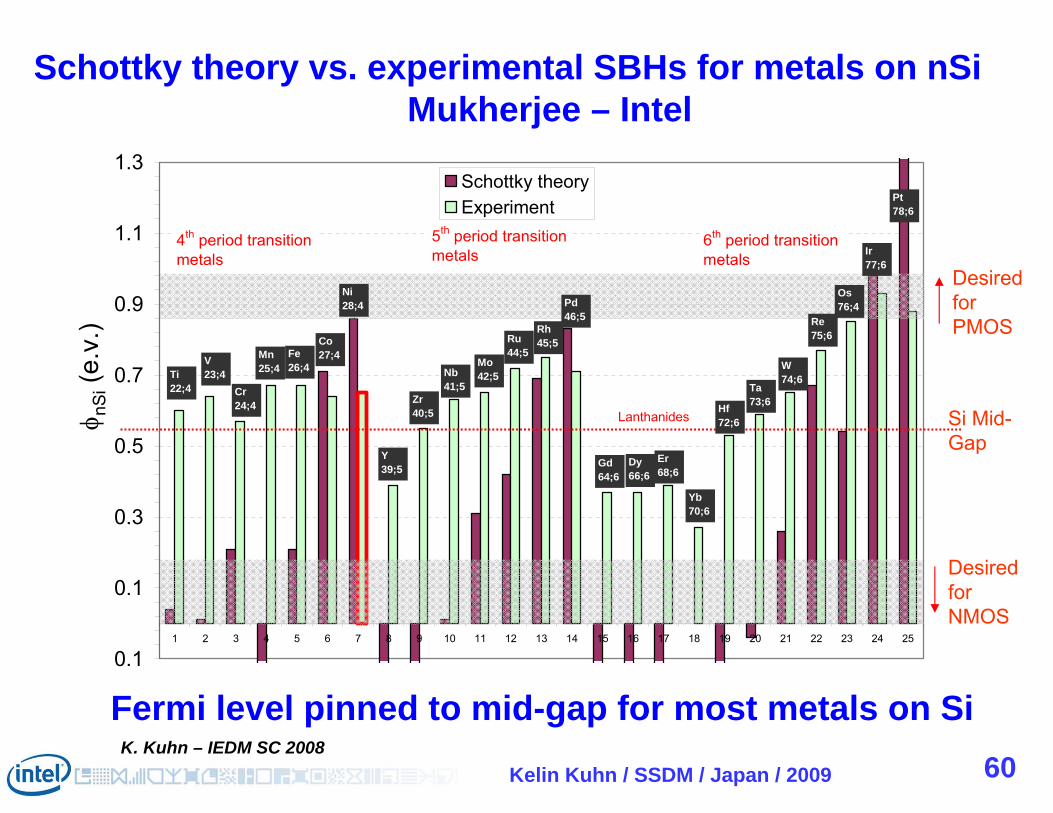
Schottky theory vs. experimental SBHs for metals on nSiMukherjee – Intel
nSi
(e.v
.)
Si Mid-Gap
0.1
0.1
0.3
0.5
0.7
0.9
1.1
1.3
1 2 3 4 5 6 7 8 9 10 11 12 13 14 15 16 17 18 19 20 21 22 23 24 25
Schottky theoryExperiment
Lanthanides
4th period transition metals
6th period transition metals
5th period transition metals
Ti22;4
V23;4
Cr24;4
Nb41;5
Zr40;5
Y39;5
Ni28;4
Co27;4Fe
26;4Mn25;4
Pt78;6
Ir77;6
Os76;4
Re75;6
W74;6
Ta73;6Hf
72;6
Er68;6
Dy66;6
Gd64;6
Pd46;5
Rh45;5Ru
44;5Mo42;5
Yb70;6
Desired for PMOS
Desired for NMOS
Fermi level pinned to mid-gap for most metals on SiK. Kuhn – IEDM SC 2008
Kelin Kuhn / SSDM / Japan / 2009 61
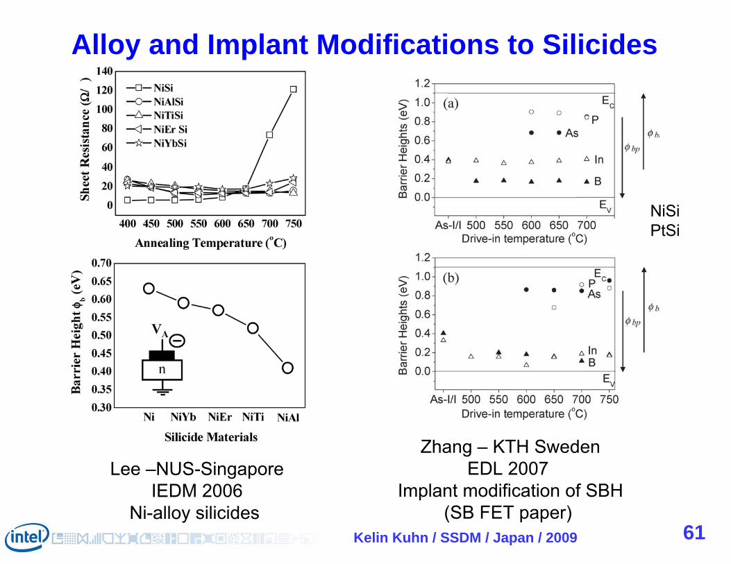
Lee –NUS-SingaporeIEDM 2006
Ni-alloy silicides
Alloy and Implant Modifications to Silicides
Zhang – KTH SwedenEDL 2007
Implant modification of SBH(SB FET paper)
NiSiPtSi
Kelin Kuhn / SSDM / Japan / 2009 62
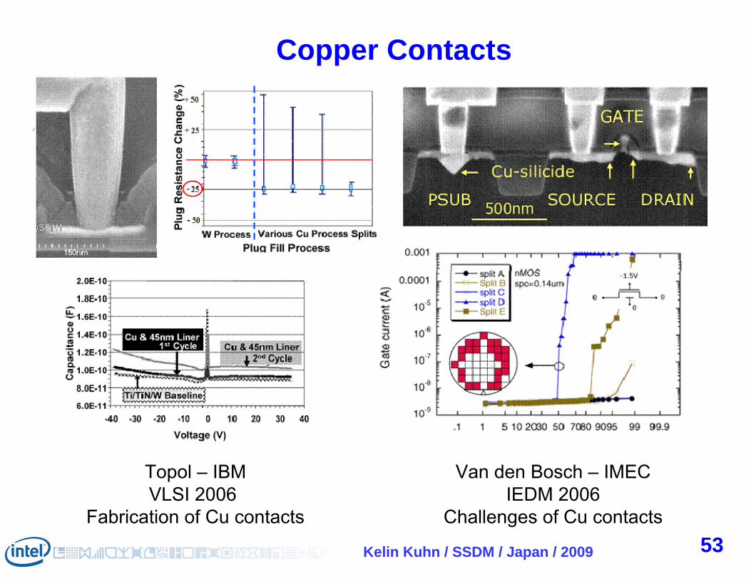
Topol – IBMVLSI 2006
Fabrication of Cu contacts
Van den Bosch – IMECIEDM 2006
Challenges of Cu contacts
Copper Contacts
53

63Kelin Kuhn / SSDM / Japan / 2009
Challenges for ALL Architectures
ResistanceCapacitance
Mobility
Kelin Kuhn / SSDM / Japan / 2009 64
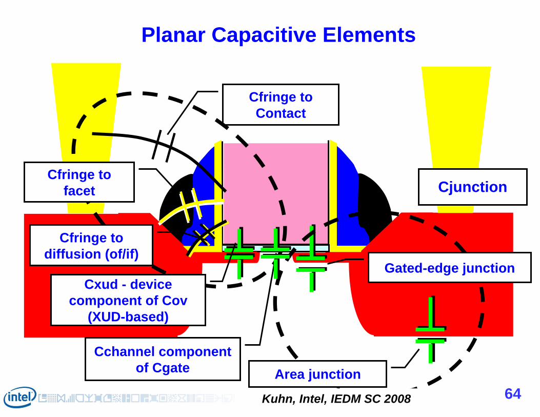
Planar Capacitive Elements
Cjunction
Area junction
Gated-edge junction
Cfringe to Contact
Cfringe to facet
Cchannel componentof Cgate
Cxud - device component of Cov
(XUD-based)
Cfringe to diffusion (of/if)
Kuhn, Intel, IEDM SC 2008
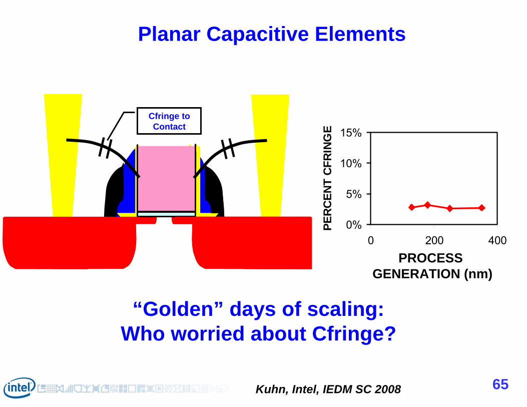
Kelin Kuhn / SSDM / Japan / 2009 65
Planar Capacitive Elements
Cfringe to Contact
“Golden” days of scaling:Who worried about Cfringe?
0%
5%
10%
15%
0 200 400GENERATION
PER
CEN
T C
FRIN
GE
PROCESS GENERATION (nm)
K. Kuhn – IEDM 2008Kuhn, Intel, IEDM SC 2008
Kelin Kuhn / SSDM / Japan / 2009 66
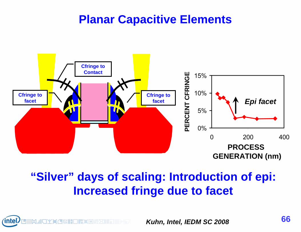
Planar Capacitive Elements
Cfringe to Contact
Cfringe to facet
Cfringe to facet
“Silver” days of scaling: Introduction of epi:Increased fringe due to facet
0%
5%
10%
15%
0 200 400GENERATION
PER
CEN
T C
FRIN
GE
Epi facet
PROCESS GENERATION (nm)
K. Kuhn – IEDM 2008Kuhn, Intel, IEDM SC 2008
Kelin Kuhn / SSDM / Japan / 2009 67
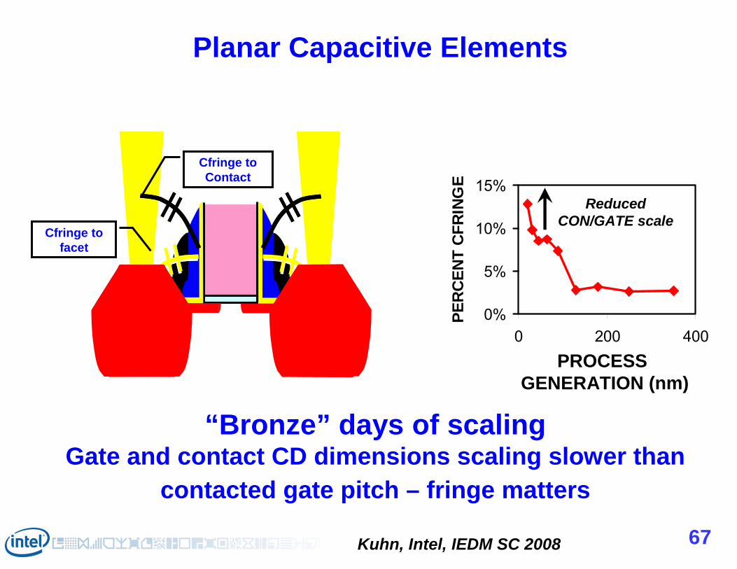
Planar Capacitive Elements
Cfringe to facet
Cfringe to Contact
“Bronze” days of scalingGate and contact CD dimensions scaling slower than
contacted gate pitch – fringe matters
0%
5%
10%
15%
0 200 400GENERATION
PER
CEN
T C
FRIN
GE
Reduced CON/GATE scale
PROCESS GENERATION (nm)
K. Kuhn – IEDM 2008Kuhn, Intel, IEDM SC 2008
Kelin Kuhn / SSDM / Japan / 2009 68
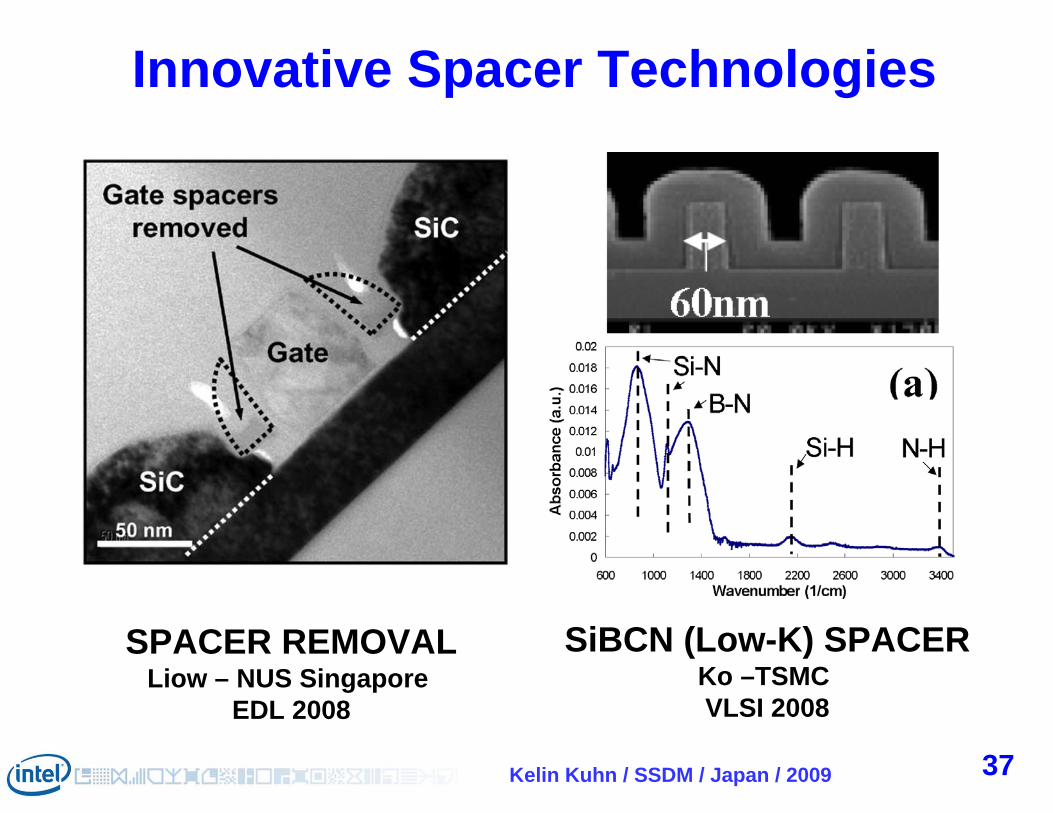
Innovative Spacer Technologies
SPACER REMOVALLiow – NUS Singapore
EDL 2008
SiBCN (Low-K) SPACERKo –TSMC VLSI 2008
37
69Kelin Kuhn / SSDM / Japan / 2009
Challenges for ALL Architectures
ResistanceCapacitance
Mobility
Kelin Kuhn / SSDM / Japan / 2009 70
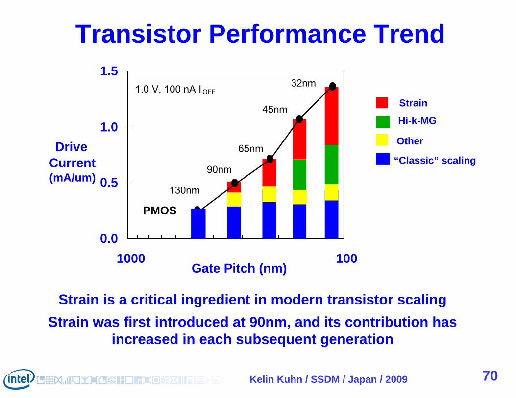
Transistor Performance Trend
Strain is a critical ingredient in modern transistor scalingStrain was first introduced at 90nm, and its contribution has
increased in each subsequent generation
Drive Current (mA/um)
1001000Gate Pitch (nm)
0.0
0.5
1.0
1.51.0 V, 100 nA IOFF
45nm
32nm
65nm
90nm
PMOS
130nm
Strain
Hi-k-MG
Other
“Classic” scaling
Kelin Kuhn / SSDM / Japan / 2009 71
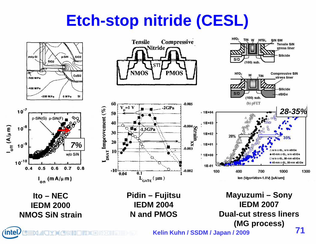
Etch-stop nitride (CESL)
Mayuzumi – SonyIEDM 2007
Dual-cut stress liners(MG process)
28-35%
Pidin – FujitsuIEDM 2004
N and PMOS
Ito – NECIEDM 2000
NMOS SiN strain
7%
Kelin Kuhn / SSDM / Japan / 2009 72
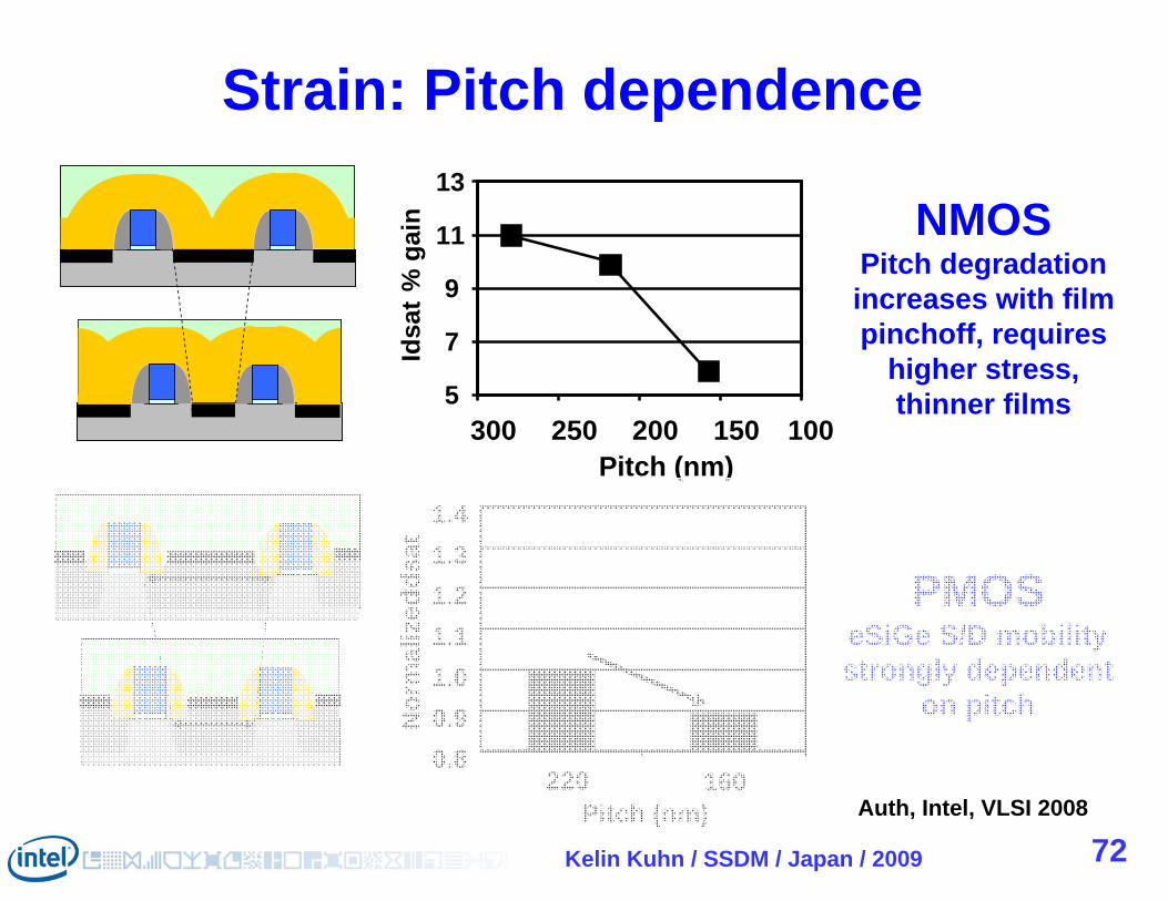
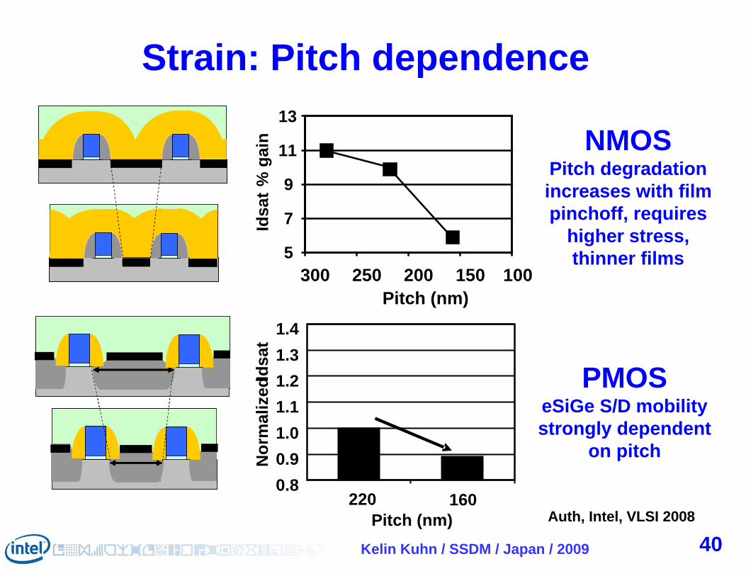
Strain: Pitch dependence
NMOS Pitch degradation increases with film pinchoff, requires
higher stress, thinner films
PMOS eSiGe S/D mobility strongly dependent
on pitch
220 160 Pitch (nm)
0.80.91.01.11.21.31.4
Nor
mal
ized
Idsa
t5
7
9
11
13
100150200250300Pitch (nm)
Idsa
t%
gai
n
Auth, Intel, VLSI 2008
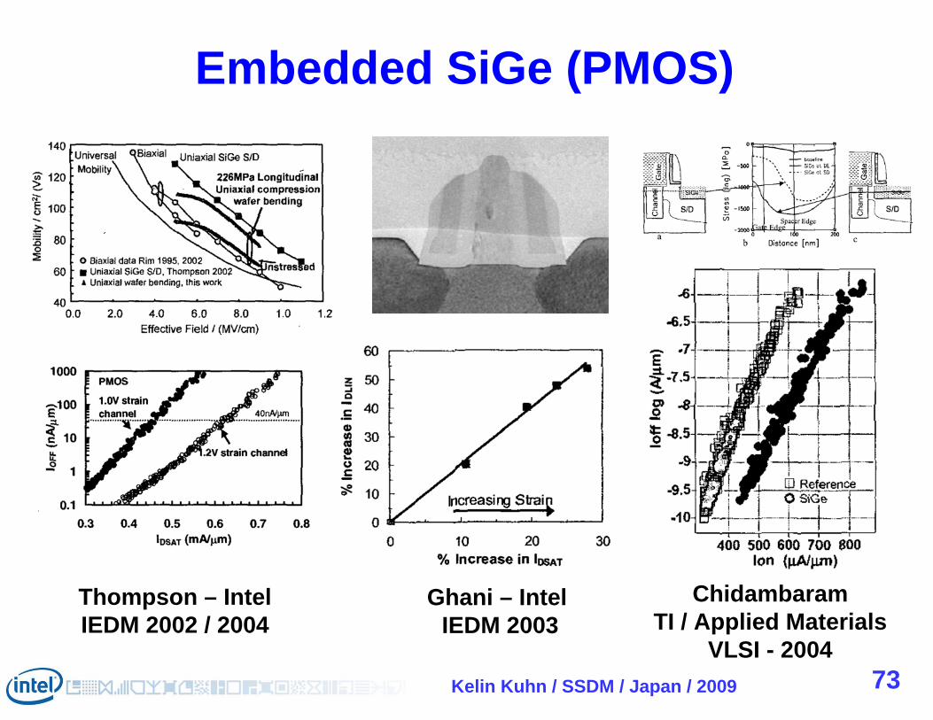
Kelin Kuhn / SSDM / Japan / 2009 73
Thompson – IntelIEDM 2002 / 2004
Ghani – Intel IEDM 2003
ChidambaramTI / Applied Materials
VLSI - 2004
Embedded SiGe (PMOS)
Kelin Kuhn / SSDM / Japan / 2009 74
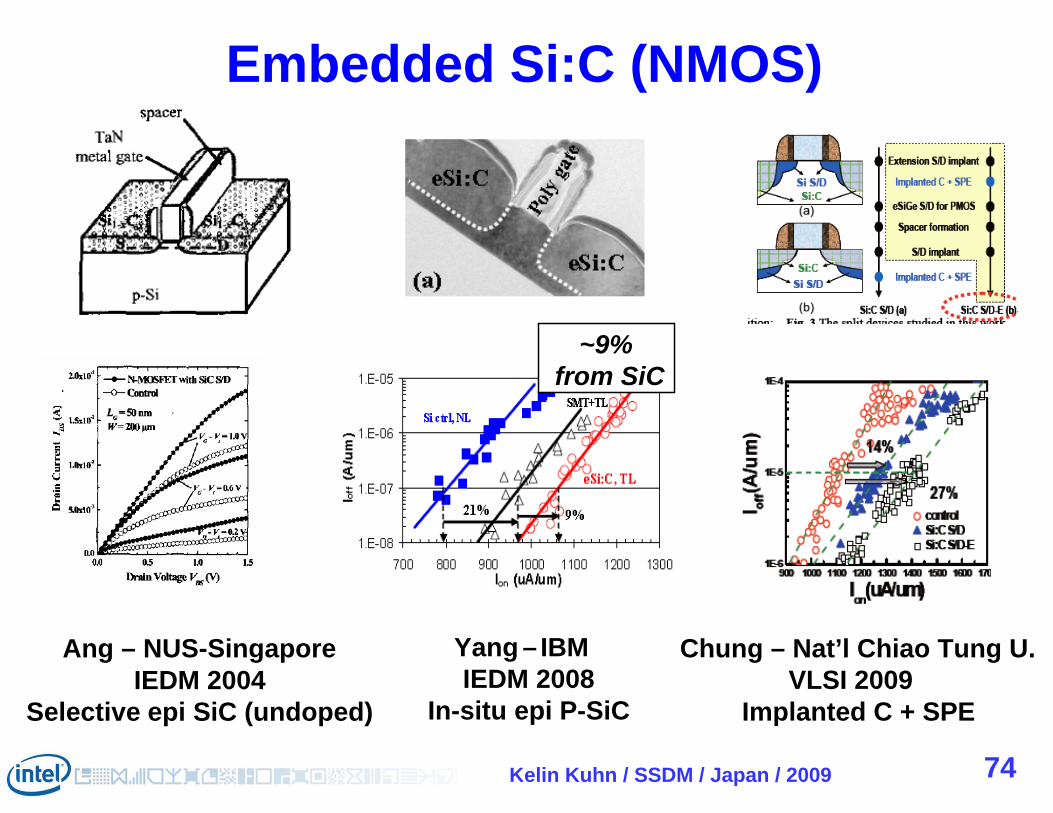
Embedded Si:C (NMOS)
Yang –IBM IEDM 2008
In-situ epi P-SiC
Ang – NUS-SingaporeIEDM 2004
Selective epi SiC (undoped)
~9% from SiC
Chung – Nat’l Chiao Tung U.VLSI 2009
Implanted C + SPE
Kelin Kuhn / SSDM / Japan / 2009 75
Strain: Pitch dependence
NMOS Pitch degradation increases with film pinchoff, requires
higher stress, thinner films
PMOS eSiGe S/D mobility strongly dependent
on pitch
220 160 Pitch (nm)
0.80.91.01.11.21.31.4
Nor
mal
ized
Idsa
t5
7
9
11
13
100150200250300Pitch (nm)
Idsa
t%
gai
n
40 Auth, Intel, VLSI 2008

Kelin Kuhn / SSDM / Japan / 2009 76
Strain: Pitch dependence
NMOS Pitch degradation increases with film pinchoff, requires
higher stress, thinner films
PMOS eSiGe S/D mobility strongly dependent
on pitch
C. Auth, VLSI 2008
220 160 Pitch (nm)
0.80.91.01.11.21.31.4
Nor
mal
ized
Idsa
t5
7
9
11
13
100150200250300Pitch (nm)
Idsa
t%
gai
n
40
What about strain options less sensitive to pitch?
Kelin Kuhn / SSDM / Japan / 2009 77
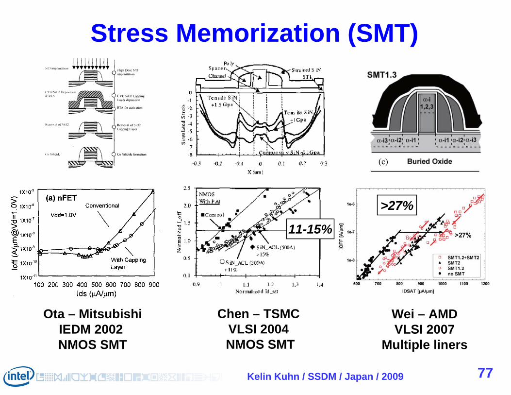
Stress Memorization (SMT)
Ota – MitsubishiIEDM 2002 NMOS SMT
Chen – TSMC VLSI 2004 NMOS SMT
Wei – AMDVLSI 2007
Multiple liners
>27%
11-15%
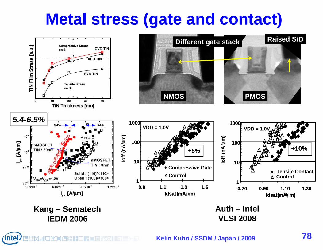
Kelin Kuhn / SSDM / Japan / 2009 78
Metal stress (gate and contact)
Auth – IntelVLSI 2008
Kang – SematechIEDM 2006
NMOS PMOS
Different gate stack Raised S/D
+10%
1
10
100
1000
0.70 0.90 1.10 1.30Idsat(mA/m)
Ioff
(nA
/m
)
Tensile ContactControl
VDD = 1.0V
+10%
1
10
100
1000
0.70 0.90 1.10 1.30Idsat(mA/m)Idsat(mA
+5%
1
10
100
1000
0.9 1.1 1.3 1.5Idsat(mA/m)
Ioff
(nA
/m
)
Compressive GateControl
VDD = 1.0V
+5%
1
10
100
1000
0.9 1.1 1.3 1.5Idsat(mA
5.4-6.5%
Kelin Kuhn / SSDM / Japan / 2009 79
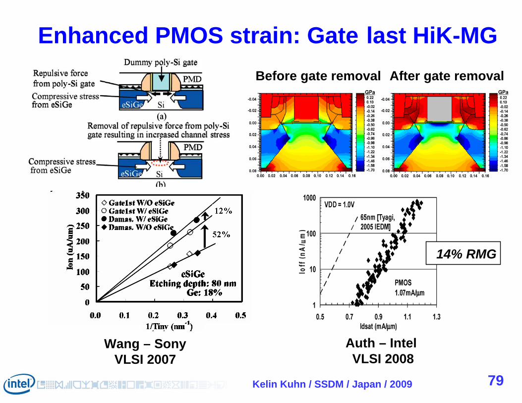
Enhanced PMOS strain: Gate last HiK-MG
Auth – Intel VLSI 2008
Before gate removal After gate removal
Wang – SonyVLSI 2007
14% RMG
Kelin Kuhn / SSDM / Japan / 2009 80
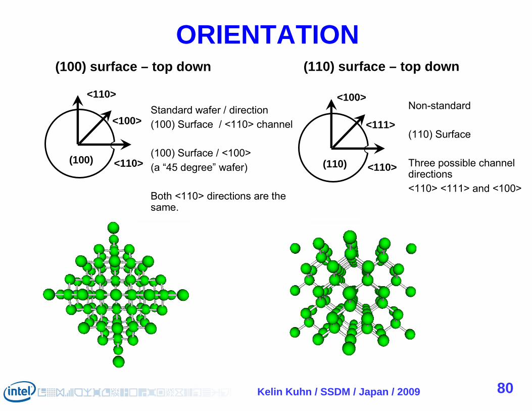
(110) surface – top down(100) surface – top down
Non-standard
(110) Surface
Three possible channel directions<110> <111> and <100>
<110>
<110>
<100>
(100)
<100>
<110>
<111>
(110)
Standard wafer / direction(100) Surface / <110> channel
(100) Surface / <100> (a “45 degree” wafer)
Both <110> directions are the same.
<100><110>
ORIENTATION

Kelin Kuhn / SSDM / Japan / 2009 81
(110) surface – top down(100) surface – top down
Non-standard
(110) Surface
Three possible channel directions<110> <111> and <100>
<110>
<110>
<100>
(100)
<100>
<110>
<111>
(110)
Standard wafer / direction(100) Surface / <110> channel
(100) Surface / <100> (a “45 degree” wafer)
Both <110> directions are the same.
<100><110>(100) BEST NMOS (110) <110> BEST PMOS
YangAMD/IBM EDST 2007
Kelin Kuhn / SSDM / Japan / 2009 82
Put NMOS at 45degrees to
PMOS?
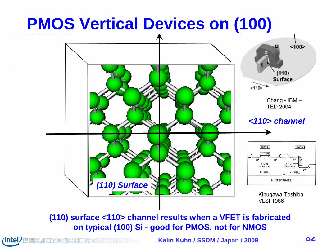
(110) Surface
(110) surface <110> channel results when a VFET is fabricated on typical (100) Si - good for PMOS, not for NMOS
<110> channel
Chang - IBM –TED 2004 [54]
Put NMOS at 45degrees to
PMOS?
(110) Surface
(110) surface <110> channel results when a VFET is fabricated on typical (100) Si - good for PMOS, not for NMOS
<110> channel
Chang - IBM –TED 2004 [54]
PMOS Vertical Devices on (100)
Kinugawa-ToshibaVLSI 1986
Kelin Kuhn / SSDM / Japan / 2009 83
Put NMOS at 45degrees to
PMOS?Put NMOS at 45degrees to
PMOS?
(100) Surface
Put NMOS at 45degrees to
PMOS?Put NMOS at 45degrees to
PMOS?
(100) Surface
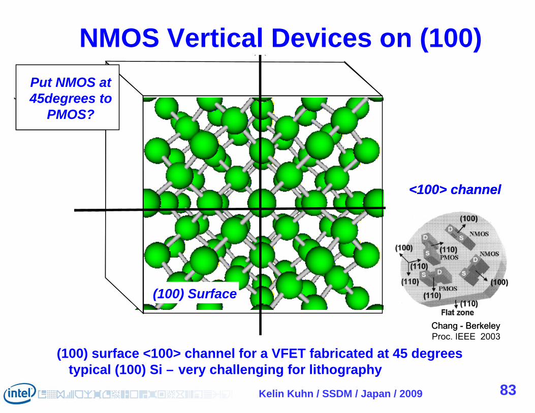
(100) surface <100> channel for a VFET fabricated at 45 degrees typical (100) Si – very challenging for lithography at 22nm node
(100) surface <100> channel for a VFET fabricated at 45 degrees typical (100) Si – very challenging for lithography
<100> channel
Chang - Berkeley Proc. IEEE 2003 [56]
<100> channel
Chang - Berkeley Proc. IEEE 2003
NMOS Vertical Devices on (100)
Kelin Kuhn / SSDM / Japan / 2009 84
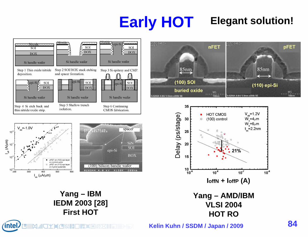
Yang – IBMIEDM 2003 [28]
First HOT
Yang – AMD/IBMVLSI 2004HOT RO
IoffN + IoffP (A)
Elegant solution!Early HOT
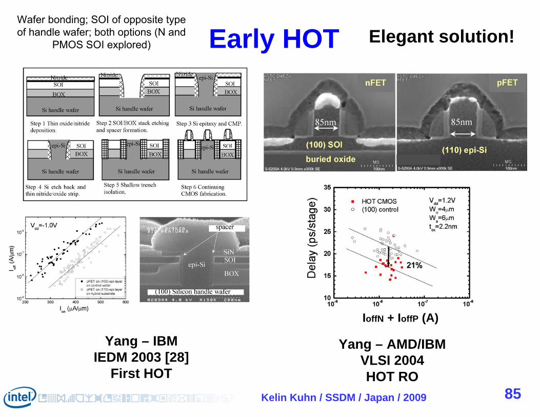
Kelin Kuhn / SSDM / Japan / 2009 85
Yang – IBMIEDM 2003 [28]
First HOT
Yang – AMD/IBMVLSI 2004HOT RO
IoffN + IoffP (A)
Elegant solution!Early HOTWafer bonding; SOI of opposite type of handle wafer; both options (N and
PMOS SOI explored)
Kelin Kuhn / SSDM / Japan / 2009 86
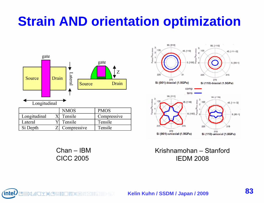
Strain AND orientation optimization
Chan – IBMCICC 2005
83
Krishnamohan – StanfordIEDM 2008
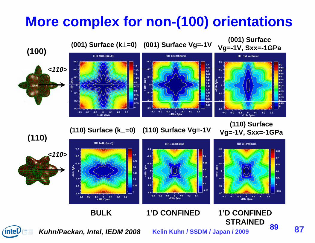
Kelin Kuhn / SSDM / Japan / 2009 8789
(110) Surface (k=0) (110) Surface Vg=-1V(110) Surface
Vg=-1V, Sxx=-1GPa
<110>
<110>
(001) Surface (k=0) (001) Surface Vg=-1V(001) Surface
Vg=-1V, Sxx=-1GPa
BULK 1’D CONFINED 1’D CONFINEDSTRAINED
(100)
(110)
More complex for non-(100) orientations
Kuhn/Packan, Intel, IEDM 2008
Kelin Kuhn / SSDM / Japan / 2009 88
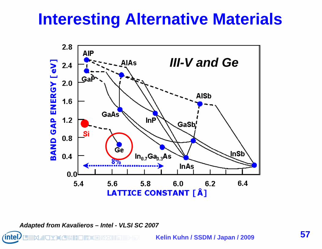
Interesting Alternative Materials
Adapted from Kavalieros – Intel - VLSI SC 200757
III-V and Ge
Kelin Kuhn / SSDM / Japan / 2009 89
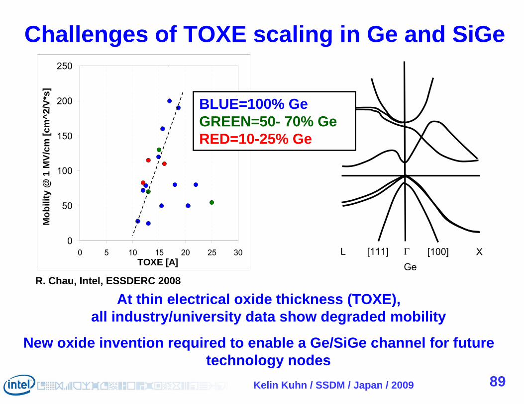
At thin electrical oxide thickness (TOXE), all industry/university data show degraded mobility
New oxide invention required to enable a Ge/SiGe channel for future technology nodes
0
50
100
150
200
250
0 5 10 15 20 25 30TOXE [A]
Mob
ility
@ 1
MV/
cm [c
m^2
/V*s
] Challenges of TOXE scaling in Ge and SiGe
R. Chau, Intel, ESSDERC 2008Ge
[100][111] XL
BLUE=100% GeGREEN=50- 70% GeRED=10-25% Ge
Kelin Kuhn / SSDM / Japan / 2009 90
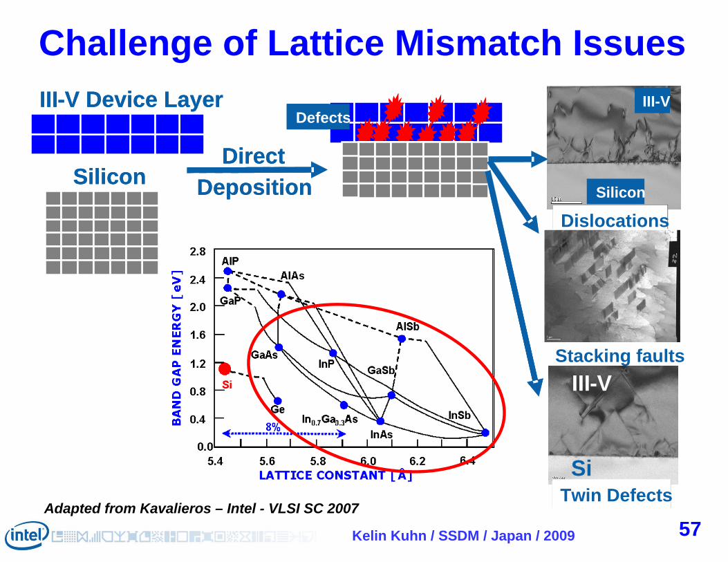
Challenge of Lattice Mismatch Issues
DirectDeposition
III-V Device Layer
SiliconDirect
Deposition
III-V Device Layer
SiliconSilicon
III-VDefects
Dislocations
Stacking faults
Si
III-V
Twin Defects
Silicon
III-V
Silicon
III-VDefectsDefects
Dislocations
Stacking faults
Si
III-V
Twin DefectsAdapted from Kavalieros – Intel - VLSI SC 2007
57
Kelin Kuhn / SSDM / Japan / 2009 91
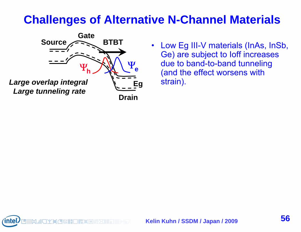
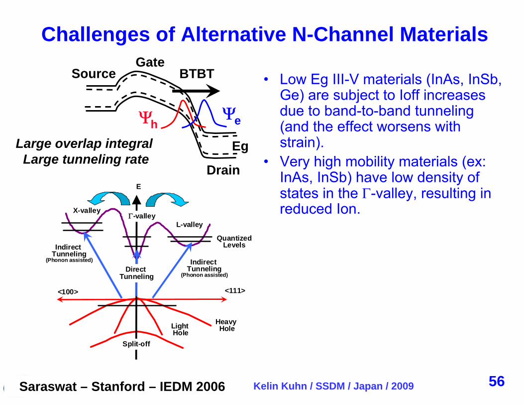
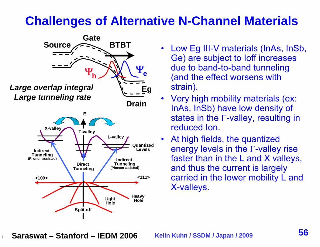
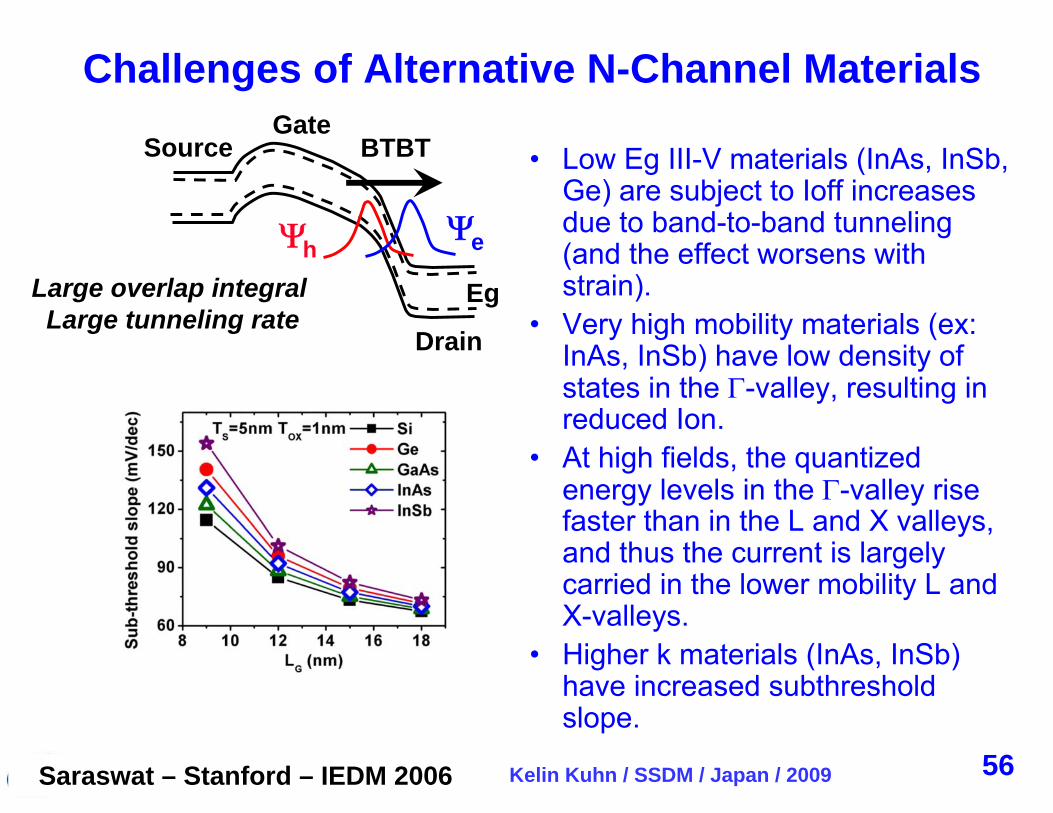
• Low Eg III-V materials (InAs, InSb, Ge) are subject to Ioff increases due to band-to-band tunneling (and the effect worsens with strain).
• Very high mobility materials (ex: InAs, InSb) have low density of states in the -valley, resulting in reduced Ion.
• At high fields, the quantized energy levels in the -valley rise faster than in the L and X valleys, and thus the current is largely carried in the lower mobility L and X-valleys.
• Higher k materials (InAs, InSb) also have increased subthresholdslope.
BTBT
Eg
Drain
SourceGate
he
Large overlap integral Large tunneling rate
56
Challenges of Alternative N-Channel Materials
Kelin Kuhn / SSDM / Japan / 2009 92
• Low Eg III-V materials (InAs, InSb, Ge) are subject to Ioff increases due to band-to-band tunneling (and the effect worsens with strain).
• Very high mobility materials (ex: InAs, InSb) have low density of states in the -valley, resulting in reduced Ion.
• At high fields, the quantized energy levels in the -valley rise faster than in the L and X valleys, and thus the current is largely carried in the lower mobility L and X-valleys.
• Higher k materials (InAs, InSb) also have increased subthresholdslope.
BTBT
Eg
Drain
SourceGate
he
Large overlap integral Large tunneling rate
56
Indirect Tunneling
(Phonon assisted) Indirect Tunneling
(Phonon assisted)
QuantizedLevels
Heavy HoleLight
HoleSplit-off
<111><100>
L-valley
X-valley-valley
E
Direct Tunneling
Saraswat – Stanford – IEDM 2006
Challenges of Alternative N-Channel Materials
Kelin Kuhn / SSDM / Japan / 2009 93
• Low Eg III-V materials (InAs, InSb, Ge) are subject to Ioff increases due to band-to-band tunneling (and the effect worsens with strain).
• Very high mobility materials (ex: InAs, InSb) have low density of states in the -valley, resulting in reduced Ion.
• At high fields, the quantized energy levels in the -valley rise faster than in the L and X valleys, and thus the current is largely carried in the lower mobility L and X-valleys.
• Higher k materials (InAs, InSb) also have increased subthresholdslope.
BTBT
Eg
Drain
SourceGate
he
Large overlap integral Large tunneling rate
56
Indirect Tunneling
(Phonon assisted) Indirect Tunneling
(Phonon assisted)
QuantizedLevels
Heavy HoleLight
HoleSplit-off
<111><100>
L-valley
X-valley-valley
E
Direct Tunneling
Saraswat – Stanford – IEDM 2006
Challenges of Alternative N-Channel Materials
Kelin Kuhn / SSDM / Japan / 2009 94
• Low Eg III-V materials (InAs, InSb, Ge) are subject to Ioff increases due to band-to-band tunneling (and the effect worsens with strain).
• Very high mobility materials (ex: InAs, InSb) have low density of states in the -valley, resulting in reduced Ion.
• At high fields, the quantized energy levels in the -valley rise faster than in the L and X valleys, and thus the current is largely carried in the lower mobility L and X-valleys.
• Higher k materials (InAs, InSb) have increased subthresholdslope.
BTBT
Eg
Drain
SourceGate
he
Large overlap integral Large tunneling rate
56Saraswat – Stanford – IEDM 2006
Challenges of Alternative N-Channel Materials
Kelin Kuhn / SSDM / Japan / 2009
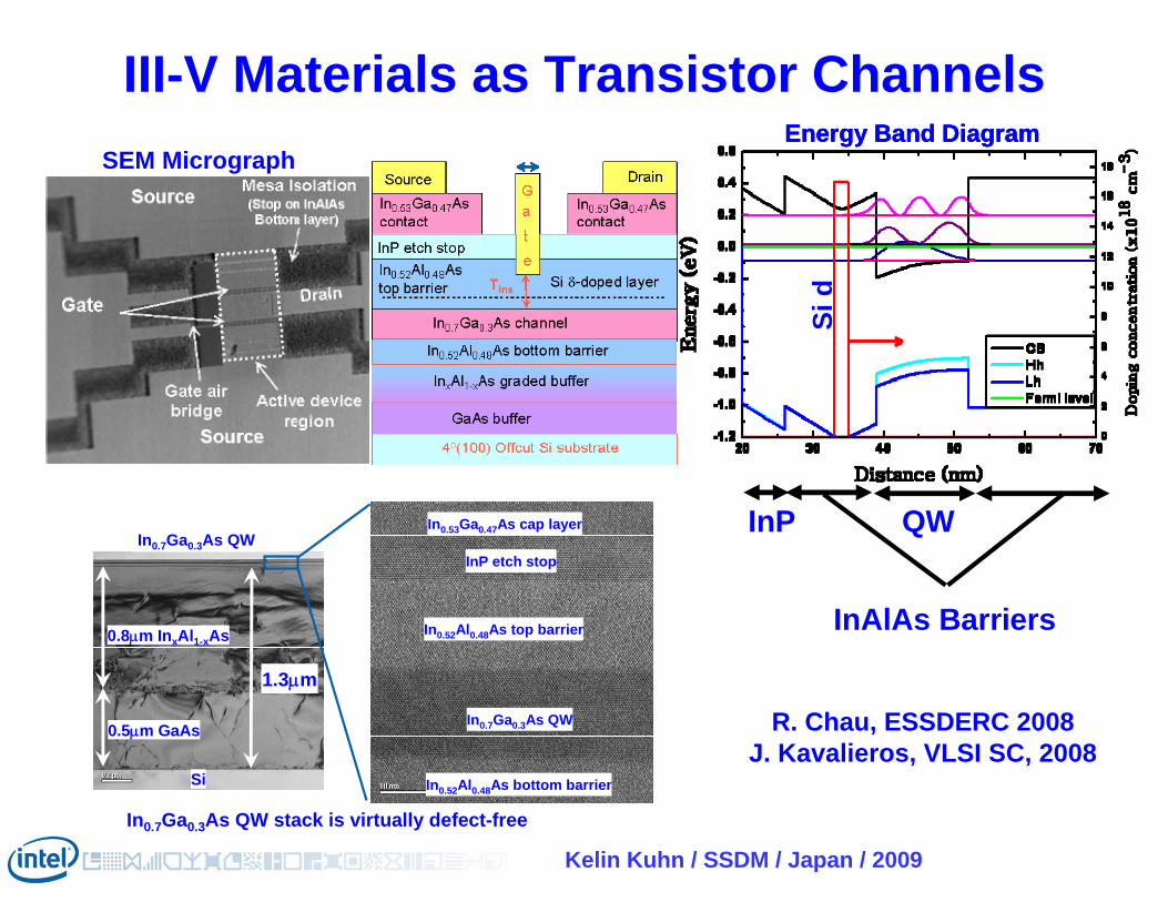
III-V Materials as Transistor Channels
0.5m GaAs
0.8m InxAl1-xAs
In0.7Ga0.3As QW
Si
1.3m
In0.7Ga0.3As QW stack is virtually defect-free
In0.52Al0.48As bottom barrier
In0.7Ga0.3As QW
In0.52Al0.48As top barrier
InP etch stop
In0.53Ga0.47As cap layer
In0.52Al0.48As bottom barrier
In0.7Ga0.3As QW
In0.52Al0.48As top barrier
InP etch stop
In0.53Ga0.47As cap layer
InAlAs Barriers
QW
SEM Micrograph
InP
Energy Band DiagramEnergy Band DiagramEnergy Band Diagram
Si d
R. Chau, ESSDERC 2008J. Kavalieros, VLSI SC, 2008

Kelin Kuhn / SSDM / Japan / 2009 96
At a gate overdrive = 0.3V, III-V QWFET shows 55% intrinsic drive current gain over strained Si
At a drain voltage of 0.5V, III-V QWFET shows >20% IDSAT gain over strained Si (despite thicker Toxe and higher RSD)
0
0.1
0.2
0.3
0.4
0.5
0.6
0 0.1 0.2 0.3 0.4 0.5
Dra
in c
urre
nt, I
D (m
A/
m)
Drain voltage, VDS
(V)
VG-V
T=0.3V
80nm InGaAs QW, TOXE=27ARSD matched to Si(Simulated)
80nm InGaAs QWTOXE=34A
40nm Strained SiTOXE=14A
2X RSD
20%
80%
Experiment & Simulation
0
0.1
0.2
0.3
0.4
0.5
0.6
0 0.1 0.2 0.3 0.4 0.5
Dra
in c
urre
nt, I
D (m
A/
m)
Drain voltage, VDS
(V)
VG-V
T=0.3V
80nm InGaAs QW, TOXE=27ARSD matched to Si(Simulated)
80nm InGaAs QWTOXE=34A
40nm Strained SiTOXE=14A
2X RSD
20%
80%
0
0.1
0.2
0.3
0.4
0.5
0.6
0 0.1 0.2 0.3 0.4 0.5
Dra
in c
urre
nt, I
D (m
A/
m)
Drain voltage, VDS
(V)
VG-V
T=0.3V
80nm InGaAs QW, TOXE=27ARSD matched to Si(Simulated)
80nm InGaAs QWTOXE=34A
40nm Strained SiTOXE=14A
2X RSD
20%
80%
Experiment & SimulationMeasurement DataMeasurement Data
0
0.1
0.2
0.3
0.4
0.5
0.6
0 0.1 0.2 0.3 0.4 0.5
Dra
in c
urre
nt, I
D (m
A/
m)
Drain voltage, VDS
(V)
VG-V
T=0.3V
80nm InGaAs QW, TOXE=27ARSD matched to Si(Simulated)
80nm InGaAs QWTOXE=34A
40nm Strained SiTOXE=14A
2X RSD
20%
80%
Experiment & Simulation
0
0.1
0.2
0.3
0.4
0.5
0.6
0 0.1 0.2 0.3 0.4 0.5
Dra
in c
urre
nt, I
D (m
A/
m)
Drain voltage, VDS
(V)
VG-V
T=0.3V
80nm InGaAs QW, TOXE=27ARSD matched to Si(Simulated)
80nm InGaAs QWTOXE=34A
40nm Strained SiTOXE=14A
2X RSD
20%
80%
0
0.1
0.2
0.3
0.4
0.5
0.6
0 0.1 0.2 0.3 0.4 0.5
Dra
in c
urre
nt, I
D (m
A/
m)
Drain voltage, VDS
(V)
VG-V
T=0.3V
80nm InGaAs QW, TOXE=27ARSD matched to Si(Simulated)
80nm InGaAs QWTOXE=34A
40nm Strained SiTOXE=14A
2X RSD
20%
80%
Experiment & SimulationMeasurement DataMeasurement Data
55%
20%
R. Chau, ESSDERC 2008
Success of III-V Materials as Transistor Channel (Vcc = 0.5V)
Kelin Kuhn / SSDM / Japan / 2009 97
AGENDA• Scaling history• Gate control
– High-k metal-gate– Structural enhancements
• Resistance• Capacitance• Mobility
– Strain– Orientation– Advanced channel materials
• Summary
98Kelin Kuhn / SSDM / Japan / 2009
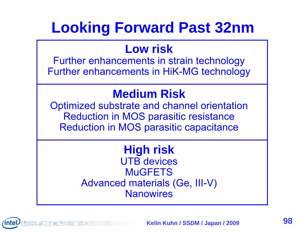
Looking Forward Past 32nmLow risk
Further enhancements in strain technologyFurther enhancements in HiK-MG technology
Medium RiskOptimized substrate and channel orientation
Reduction in MOS parasitic resistanceReduction in MOS parasitic capacitance
High riskUTB devices MuGFETS
Advanced materials (Ge, III-V) Nanowires

Kelin Kuhn / SSDM / Japan / 2009 99
Questions???Questions???