kenneth r. laker, university of pennsylvania, updated 6apr15
TRANSCRIPT

Kenneth R. Laker, University of Pennsylvania, updated 6Apr15
1

Kenneth R. Laker, University of Pennsylvania, updated 6Apr15
2
Extract Parasitic Elements
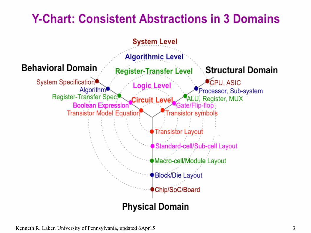
Three Domain View of VLSI Design Flow at One Level
1. Design Rule Check (DRC)2. Layout Versus Schematic (LVS) Check3. Post layout simulation (PLS)
SPICE(Spectre)
Verilog/Cadence
Cadence(Virtuoso)
PLS
Verilog/Spectre
FUNCTIONAL DESIGN
Verilog/Spectre
Spectre
LAYOUTVERIFICATION
Kenneth R. Laker, University of Pennsylvania, updated 6Apr15
3

Kenneth R. Laker, University of Pennsylvania, updated 6Apr15
4
(and near neighbor boundaries)
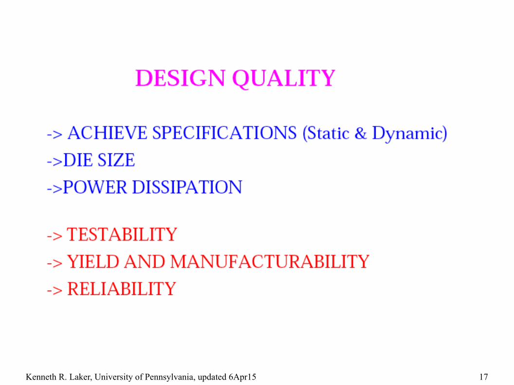
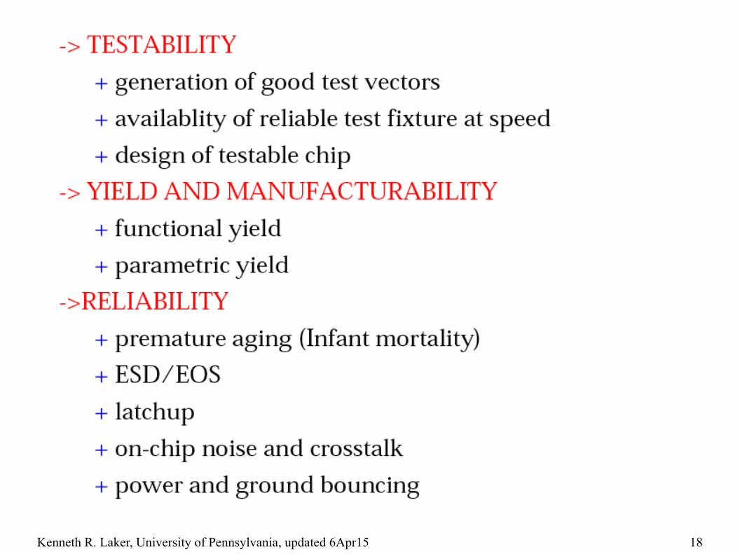
Metrics By Which Design Success is Measured:
metrics.

Kenneth R. Laker, University of Pennsylvania, updated 6Apr15
5

Kenneth R. Laker, University of Pennsylvania, updated 6Apr15
6
add4
add add addadd
sum
car ry
sum
car ry
sum
car ry
sum
car ry
nand
nor
nand
nor
nand
nor
nand
nor
Hierarchical & Modular 4-bit Adder
+ab
c
co
s
inv inv inv inv
cab sumcab carry
s
co
++++
a[3:0]
b[3:0]s[3:0]
co3
c0

Kenneth R. Laker, University of Pennsylvania, updated 6Apr15
7
++++
a[3:0]
b[3:0]s[3:0]
co3
c0
a[0]
a[1]
a[2]
a[3]
b[0]
b[1]
b[2]
b[3]s[3]
s[2]
s[1]
s[1]add[0]
add[1]
add[2]
add[3]
c0
co3
(100,100)
(100,200)
(100,300)
(100,400)
(0,100)(0,0)
b[i]
a[i]s[i]
c[i]
co[i]
add[i]
(100,100)
(100,50)
(100,0)(50,0)
(50,100)
(0,0)
(0,25)
(0,75)
add4 Module
add1 Celladd4
Hierarchical & Modular Layout

Kenneth R. Laker, University of Pennsylvania, updated 6Apr15
8
Unused die area -> inefficient layout
Structural Hierarchy 1 mapped poorly intoPhysical Hierarchy.
Better mapping!
Miss-mappings between Structural and Physical Hierarchies usually avoided by using automatic layout system.

Kenneth R. Laker, University of Pennsylvania, updated 6Apr15
9
REGULARITYDESIGN THE CHIP REUSING AS MANY IDENTICAL MODULES, CIRCUITS, DEVICES AS POSSIBLE. REGULARITY CAN EXIST AT ALL LEVELS OF THE DESIGN HIERARCHY.
sub-structures.

Kenneth R. Laker, University of Pennsylvania, updated 6Apr15
10
LOCALITY (PHYSICAL)TIME LOCALITY: modules are synchronized by common clock.
-> Critical timing paths are kept within module boundaries or within near neighbor Boundaries.
-> Place modules to minimize large or “global” inter-module signal routes.
-> Care take to realize robust clock generation and distribution.
-> Signal routes between modules with large physical separation need sufficient time to traverse route.
-> Replicate modules, if necessary, to alleviate delay issues caused by long inter- module signal routes.
Take care

Kenneth R. Laker, University of Pennsylvania, updated 6Apr15
11
Performance Increasing, Die Area Decreasing, Power Dissipation Increasing (for a given application)
Design Time and Cost Decreasing (for a given application)

Kenneth R. Laker, University of Pennsylvania, updated 6Apr15
12
are
custom design style.

Kenneth R. Laker, University of Pennsylvania, updated 6Apr15
13
Gates/Modules:
Gate/Module standard cell concept can be extended to higher level functions, often as parameterized modules.

Kenneth R. Laker, University of Pennsylvania, updated 6Apr15
14
Kenneth R. Laker, University of Pennsylvania, updated 6Apr15
15
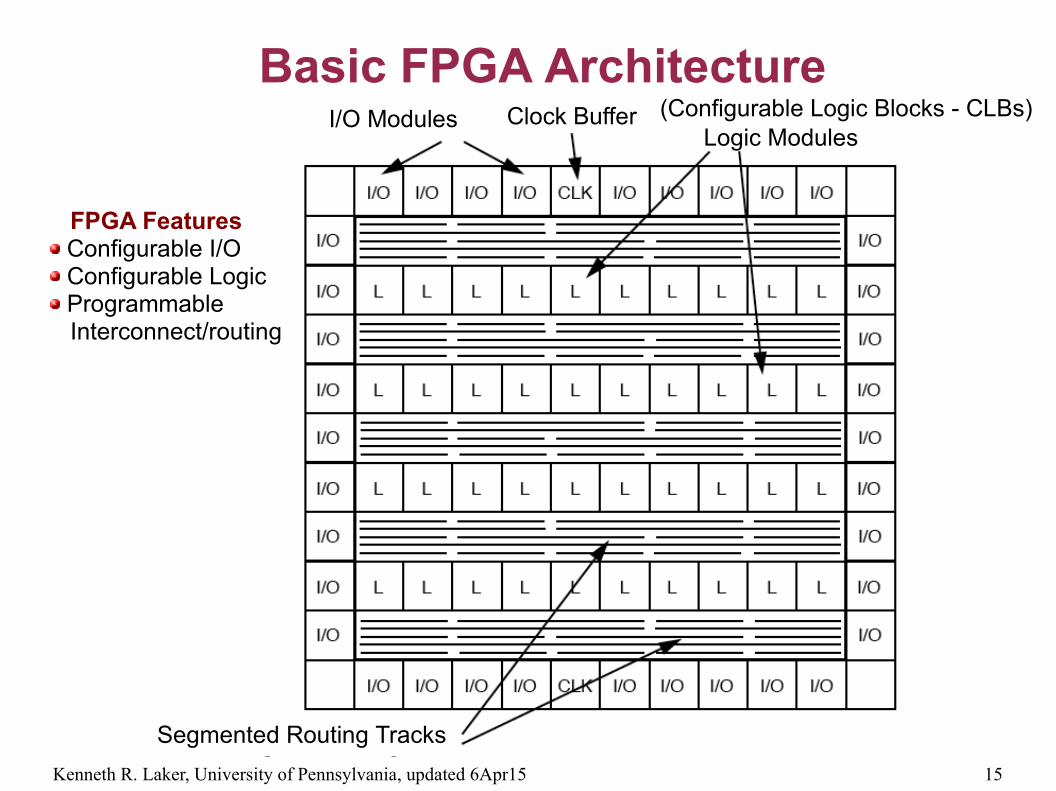
Basic FPGA Architecture(Configurable Logic Blocks - CLBs)
Segmented Routing Tracks
I/O ModulesLogic Modules
Clock Buffer
FPGA Features Configurable I/O Configurable Logic Programmable
Interconnect/routing

Kenneth R. Laker, University of Pennsylvania, updated 6Apr15
16http://www.latticesemi.com/products/fpga/ecp2/optimizedfpgaarchitecture.cfm
State-of-the-Art FPGA Architecture
Programmable Function Unit (PFU) – perform logic, arithmetic,Distributed RAM & ROM functions.
Flexible Sys I/O Buffers – support LVCMOS, LVDS, etc.
Sys Clock – PLLs & DLLs for clock management.
Configuration Port – supports SPI, serial and parallel configuration.
Sys DSP Blocks – implement multipliers, adders, subtractors,accumulators.
Embedded 3.125 Gbps SERDES – support PCI express, Ethernet.
TransFR = Transparent Field ReconfigurationTransFR I/O
Kenneth R. Laker, University of Pennsylvania, updated 6Apr15
17
Kenneth R. Laker, University of Pennsylvania, updated 6Apr15
18

Kenneth R. Laker, University of Pennsylvania, updated 6Apr15
19
IMPORTANT PACKAGE DESIGN CONCERNS:

Kenneth R. Laker, University of Pennsylvania, updated 6Apr15
20
Package Bonding Techniques

Kenneth R. Laker, University of Pennsylvania, updated 6Apr15
21
Parasitics in an Electronic Package
PCB Transmission Line
PCB Ground PlanePCB Vias
Wire Bond Package Body
DiePaddle
Kenneth R. Laker, University of Pennsylvania, updated 6Apr15
22
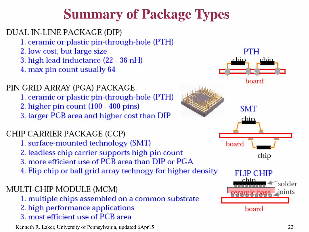
Summary of Package Types

Kenneth R. Laker, University of Pennsylvania, updated 6Apr15
23
A System-In-Package Solution
http://www.ansoft.com/leadinginsight/pdf/System%20in%20Package.pdf, slide 15
chipHigh density memory chip