keysight technologies measure parasitic capacitance and...
TRANSCRIPT

Keysight TechnologiesMeasure Parasitic Capacitance and Inductance Using TDR
White Paper

02 | Keysight | Measure Parasitic Capacitance and Inductance Using TDR – White Paper
Time Domain Reflectometry (TDR) is commonly used as a convenient method to de-termine the characteristic impedance of a transmission line, or to quantify reflections caused by discontinuities along or at the termination of a transmission line. TDR can also be used to measure quantities such as the input capacitance of a voltage probe, the inductance of a jumper wire, the end to end capacitance of a resistor, or the effective loading of a PCI card. Element values can be calculated directly from the integral of the reflected or transmitted waveform.
David J. DascherKeysight Technologies, Inc.Colorado Springs, CO, USA
Why would anyone use TDR to measure an inductance or capacitance when there are many Inductance-Capacitance-Resistance (LCR) meters available that have excellent resolution and are easy to use? First of all, TDR allows measurements to be made on de-vices or structures as they reside in the circuit. When measuring parasitic quantities, thephysical surroundings of a device may have a dominant effect on the quantity that is being measured. If the measurement can not be made on the device as it resides in the circuit, then the measurement may be invalid. Also, when measuring the effects of devices or structures in systems containing transmission lines, TDR allows the user to separate the characteristics of the transmission lines from the characteristics of the device or structure being measured without physically separating anything in the circuit. To illustrate a case where TDR can directly measure a quantity that is very difficult to measure with an LCR meter, consider the following example.
A Printed Circuit (PC) board has a long, narrow trace over a ground plane which forms a “micro-strip” transmission line. At some point, the trace goes from the top of the PC board, through a via, to the bottom of the PC board and continues on.The ground plane has a small opening where the via passes through it. Assuming that the via adds capacitance to ground, a model of this structure would be a discrete capac-itance to ground between the top and bottom transmission lines. For now, assume that the characteristics of the transmission lines are known and all that needs to be measured is the value of capacitance to ground between the two transmission lines.
Using an LCR meter, the total capacitance between the trace-via-trace structure and ground can be measured but the capacitance of the via can not be separated from the capacitance of the traces. Sacrificing this PC Board for the sake of science, the trac-es are cut away from the via. Now the capacitance between just the via and ground is measured. Unfortunately, the measured value is not the correct value of capacitance for the model.
Using TDR instead of an LCR meter, a step shaped wave is sent down the trace on the PC board and the wave that gets reflected off of the discontinuity caused by the via is observed. The amount of “excess” capacitance caused by the via can be calculated by integrating and scaling the reflected waveform. Using this method, the measured value of capacitance is the correct value of capacitance to be used in the model.
The discrepancy between the two measurements is that an LCR meter measures the total capacitance of the via while TDR measures the “excess” capacitance of the via. If the series inductance of the via was 0, then its total capacitance would be the same as its excess capacitance. Since the series inductance of the via is not 0, a complete model of the via must include both its series inductance and shunt capacitance. Assuming that the via is “capacitive”, the complete model can be accurately simplified by removing the series inductance and including only the excess capacitance rather than the total capacitance.

03 | Keysight | Measure Parasitic Capacitance and Inductance Using TDR – White Paper
It should be no surprise that the value of excess capacitance measured using TDR is the correct value for the model. The reason to model the trace-via-trace structure in the first place is to predict what effect the via will have on signals propagating along the trac-es. TDR propagates a signal along the trace in order to make the measurement. In this sense, TDR provides a direct measurement of the unknown quantity.
To derive expressions that relate TDR waveforms to excess capacitance and inductance, an understanding of the fundamental transmission line parameters is required. A cursory review of transmission lines and the use of TDR to characterize them will be presented prior to deriving expressions for excess capacitance and inductance. If you are already familiar with transmission lines and TDR then you may wish to skip the next sections.
Fundamental transmission line parameters:First, a bit about “Ground”. Twin-lead (or twisted pair) forms a two conductor transmis-sion line structure that can be modeled as shown in figure 1. The model includes the self inductance of each conductor, mutual inductance between the self inductances, and capacitance between the two conductors. Skin effect and dielectric loss are assumed to be negligible in this model. Injecting a current transient into one side of the transmissionline, from node A1 to node C1, causes a voltage (v=i*Z0) to appear between nodes A1 and C1 and also causes a voltage (v=L*di/dt) to appear across the series inductance of both the A-B and C-D conductors. Referring back to the physical structure, this means that there is a voltage difference between the left side and right side of each conductor. Even if you name the C-D conductor “Ground”, it still develops a voltage between its left side and right side, across its series inductance.
Microstrip traces and coaxial cables (coax) are two very special cases of two conductortransmission line structures. Injecting a current transient into one side of a microstrip or coax transmission line causes a voltage to appear across only one of the two conductors. In the case of ideal microstrip, where one of the conductors is infinitely wide, the wide conductor can be thought of as a conductor with 0 inductance. Hence the voltage gen-erated across the infinitely wide conductor is 0. With coax, the inductance of theouter conductor is not 0. The voltage generated across the inductance of the outer conductor has two components. One component is due to the current through the self inductance of the outer conductor (v1=Loc*di/dt). The other component is due to the current through the center conductor and the mutual inductance between the center and outer conductors (v2=Lm*di/dt). Current that enters the center conductor returns through the outer conductor so the two currents are equal but in opposite directions.The unique property of coax is that the self inductance of the outer conductor is exactly equal to the mutual inductance between the center and the outer conductors. Hence the two components that contribute to the voltage generated across the inductance of the outer conductor exactly cancel each other and the resulting voltage is 0. When current is injected into a coax transmission line, no voltage is generated along the outer conductor if the current in the center conductor is returned in the outer conductor.
The point here is that the generalized model for a two conductor transmission line can be simplified for microstrip and coax constructions. The simplified model has zero inductance in series with one of the conductors since, in both cases, no voltage appears across the conductor. This conductor is commonly referred to as the ground plane in microstrip transmission lines and as the shield in coax transmission lines. The other con-ductor, the one that develops a voltage across it, is referred to as the “transmission line”, even though it is really only half of the structure.
There are two ways to model a lossless transmission line. One method defines the trans-mission line in terms of characteristic impedance (Z0) and time delay (td) and the other method defines the transmission line in terms of total series inductance (LTotal) and total shunt capacitance (CTotal). There are times when it is beneficial to think of a transmission line in terms of Z0 and td and likewise, there are times when thinking in terms of CTotal and LTotal is best.

04 | Keysight | Measure Parasitic Capacitance and Inductance Using TDR – White Paper
If one end of a long transmission line is driven with an ideal current step, the voltage at that end will be an ideal voltage step whose height is proportional to the current and the characteristic impedance (Z0) of the transmission line, VIn=IIn*Z0. The waveform generated at this end will propagate along the transmission line and arrive at the opposite endsome time later. The time it takes the wave to propagate from one end to the other is the time delay (td) of the transmission line.
The total capacitance and inductance of a transmission line can be measured with an LCR meter. To determine the total capacitance of a coaxial cable, measure the capac-itance between the center conductor and the shield at one end of the cable while the other end is left open. The frequency of the test signal used by the LCR meter should be much less than 1/(4*td) where td is the time delay of the cable. To measure the total inductance of the cable, measure the inductance from the center conductor to the shield at one end of the cable while the other end has the center conductor connected tothe shield. Again, the test frequency must be much less than 1/(4*td).
If the characteristic impedance and time delay of a transmission line are known, then the total shunt capacitance and total series inductance of the transmission line can be calculated as:
If the total shunt capacitance and total series inductance are known, then td and Z0 can be calculated as:
As an example, many engineers use 50 ohm coaxial cables that are about 4 feet long and have BNC connectors on each end. The time delay of these cables is about 6 nanosec-onds (nS), the capacitance of the cable is 6nS/50ohms = 120 picofarads (pF), and the inductance of the cable is 6nS*50ohms = 300 nanohenrys (nH).
CtZ
L t ZTotald
Total d ⋅==0
0
Total
TotalTotalTotald C
LZCLt =⋅= 0

05 | Keysight | Measure Parasitic Capacitance and Inductance Using TDR – White Paper
Figure 2 shows two LC models for a 50 ohm, 6 nS long coaxial cable. The distributed in-ductance of the transmission line has been collected into 2 discrete inductors in the first model and 6 discrete inductors in the second model. The distributed capacitance has been collected into 1 discrete capacitor in the first model and 5 discrete capacitors in the second. Collecting the distributed capacitance and inductance into discrete, lumpedelements reduces the range of frequencies over which the model is accurate. The more discrete segments that a transmission line is broken up into, the wider range of fre-quencies the model is accurate over. Figure 3 shows the magnitude of the impedance seen looking into one end of each model while the other end is left open. The 5 segment model is accurate over a wider range of frequencies than the 1 segment model. Figure 3 also shows the transmitted response through each of the models in a circuit that is both source and load terminated in 50 ohms. The discrete LC models are both low pass filters.
Figure 2
1
51
51
51
5103
1 2 4 6 8 1 2 4 6 8 1 2 4 6
106
108
3
4
5
67891
2
10-1
mag(ZIn_TLine)mag(ZIn_1Seg)mag(ZIn_5Seg)
mag(Out_TLine/In)mag(Out_1Seg/In)mag(Out_5Seg/In)
Figure 3
freq

06 | Keysight | Measure Parasitic Capacitance and Inductance Using TDR – White Paper
Again, the 5 segment model is accurate over a wider range of frequencies than the 1 seg-ment model. In the time domain, a good rule of thumb is to break a transmission line into 5 segments per risetime. For example, to build a model that will accurately simulate the response of a step with a 1 nanosecond risetime, the model should contain 5 segments per nanosecond of time delay. This would require a 30 segment model for the 4 foot, 6 nS coaxial cable.
The transmission line model used in SPICE and many other time domain simulators is defined by characteristic impedance and time delay. It consists only of resistors, depen-dent sources, and time delay. It is an accurate model of a lossless transmission line over an infinite range of frequencies. There are three situations where lumped LC models may be preferred over the Z0-td model used by SPICE. When modeling very short sections of transmission lines, the maximum time increment is never greater than the time delay ofthe shortest transmission line. Short transmission lines can cause lengthy simulations. When modeling skin effect and dielectric loss, discrete LC models can be modified to include these effects. And finally, discrete LC models can be used to model transmission line systems that contain more than two conductors.
Characteristic impedance and time delay, or series inductance and shunt capacitance, completely specify the electrical properties of a lossless transmission line. Propagation velocity and length are also required in order to completely specify a physical cable or PC board trace. If the time delay (also known as the electrical length) of a cable is 6 nS and the physical length of the cable is 4 feet, then the propagation velocity is .67 feet per nanosecond. The propagation delay is 1.5 nS per foot.
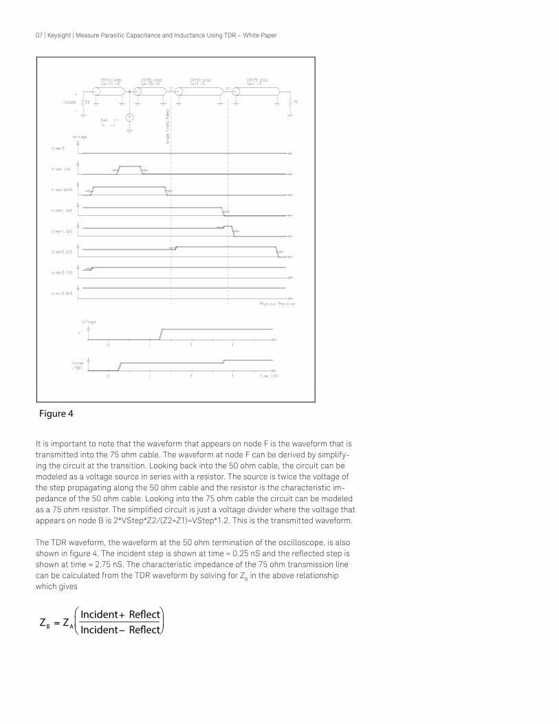
Reflection coefficients for impedance changes:Figure 4 shows a typical measurement setup using an oscilloscope with an internal TDR. The oscilloscope input is a 50 ohm transmission line terminated into 50 ohms. The TDR step generator can be modeled as a current source that connects to the 50 ohm trans-mission line between the front of the oscilloscope and the 50 ohm termination. When the current source transitions from low to high at time = 0, voltages are generated in the system as shown. Note that figure 4 is plotting voltage versus position along the trans-mission lines, not versus time. The waveform viewed by the oscilloscope is the waveform at the 50 ohm termination. This is the TDR waveform.
There is only one discontinuity in the system, the transition between the 50 ohm cable and the 75 ohm cable at node “F”. When the wave propagating along the 50 ohm trans-mission line arrives at the 75 ohm transmission line, reflected and transmitted waves are generated The wave that is incident to the transition is shown at time=1.2nS. Waves that are reflected and transmitted from the transition are shown at time=1.3nS. Defining a positive reflected wave to be propagating in the opposite direction as the incident wave, the reflected wave is given as:
where ZA is the characteristic impedance that the incident wave travels through and ZB is the characteristic impedance that the transmitted wave travels through. The transmitted wave is given as:
If ZA = 50 ohms, ZB = 75 ohms, and the incident waveform is a 1 volt step then the reflect-ed waveform will be a step of 1*(75-50)/(75+50) = 0.2 volts and the transmitted wave-form will be a step of 1*(2*75)/(75+50) = 1.2 volts.
re�ectedincident
Z ZZ Z
B A
B A
=−+
transmittedincident
ZZ Z
B
B A
=⋅+
2
07 | Keysight | Measure Parasitic Capacitance and Inductance Using TDR – White Paper
Figure 4
It is important to note that the waveform that appears on node F is the waveform that is transmitted into the 75 ohm cable. The waveform at node F can be derived by simplify-ing the circuit at the transition. Looking back into the 50 ohm cable, the circuit can be modeled as a voltage source in series with a resistor. The source is twice the voltage of the step propagating along the 50 ohm cable and the resistor is the characteristic im-pedance of the 50 ohm cable. Looking into the 75 ohm cable the circuit can be modeled as a 75 ohm resistor. The simplified circuit is just a voltage divider where the voltage that appears on node B is 2*VStep*Z2/(Z2+Z1)=VStep*1.2. This is the transmitted waveform.
The TDR waveform, the waveform at the 50 ohm termination of the oscilloscope, is also shown in figure 4. The incident step is shown at time = 0.25 nS and the reflected step is shown at time = 2.75 nS. The characteristic impedance of the 75 ohm transmission line can be calculated from the TDR waveform by solving for ZB in the above relationshipwhich gives
Z ZIncident Re�ectIncident Re�ectB A=
+−

08 | Keysight | Measure Parasitic Capacitance and Inductance Using TDR – White Paper
Both the incident and reflected waveforms are step functions that differ only in ampli-tude and direction of propagation. In the expression for ZB, the step functions cancel and all that remains is the step heights. The TDR waveform in figure 4 shows the incident step height to be +1 volt and the reflected step height to be +0.2 volts. Knowing the imped-ance looking into the oscilloscope is ZA = 50 ohms, the characteristic impedance of the second cable, ZB, can be calculated as ZB = 50*(1V+0.2V)/(1V-.2V) = 75 ohms.
There is a “transition” from the front panel of the oscilloscope to the first cable. The characteristic impedance on either side of the transition is the same, hence the reflected wave has 0 amplitude. If there is no reflected wave, then the transmitted wave is iden-tical to the incident wave. Electrically, there is no discontinuity at this transition since it causes no reflection and the transmitted wave is identical to the incident wave.
The transition between transmission lines of different characteristic impedance is a discontinuity that produces reflected and transmitted waves that are identical in shape to the incident wave. The reflected wave differs from the incident wave in amplitude and direction of propagation. The transmitted wave differs only in amplitude. Discontinuities that are not simply impedance changes will produce reflected and transmitted waves that are different in shape from the incident wave.

09 | Keysight | Measure Parasitic Capacitance and Inductance Using TDR – White Paper
Discrete shunt capacitance:
Figure 5 shows two 50 ohm transmission lines with a shunt capacitor between them. The capacitance produces a discontinuity between the two transmission lines. A wave that is incident to the discontinuity produces reflected and transmitted waves. In this case, both the reflected and transmitted waves have a different shape than the incident wave.
Given an incident step, the voltage at node “H” can be ascertained by simplifying the circuit as shown in figure 5. The incident step, shown at time = 1.8 nS, has an amplitude of “inc_ht” and is propagating along a 50 ohm transmission line. Looking to the left of the capacitor, the circuit can be simplified as a voltage source in series with a resistor. The voltage source is twice the incident voltage and the resistance is Z0=50 ohms (not RS=50 ohms). Looking to the right of the capacitor, the circuit can be simplified as a resistor of value Z0=50 ohms (not RL=50 ohms). The simplified circuit contains no transmission lines. The circuit can again be simplified by combining the two resistors and the voltage source into their Thevenin equivalent.
Note that if the left transmission line did not have a source resistance of 50 ohms, or the right transmission line did not have a load resistance of 50 ohms, the simplified model would still be valid for 10 nS after the incident step arrives at node H. After 10 nS, reflec-tions from the source and load terminations would need to be accounted for at node H.
Looking at the simplified circuit and redefining time = 0 to be when the incident steparrives at node H, the voltage at node H is 0 for time < 0. For time > 0, the voltage at node H is
V
Where
H = −
= ⋅ = ⋅
−inc ht e
R CZ
C
t
_ 1
20
τ
τ
Figure 5

10 | Keysight | Measure Parasitic Capacitance and Inductance Using TDR – White Paper
The voltage waveform that appears on node H is the transmitted waveform. The reflect-ed wave can be determined knowing that the incident wave equals the transmitted wave plus the reflected wave. For time < 0, the reflected wave is 0. For time > 0, the reflected wave is
Normalizing the reflected waveform to the incident step height and integrating the nor-malized reflected waveform gives
Solving for the shunt capacitance between the two transmission lines gives
The amount of capacitance between the two transmission lines can be determined by integrating and scaling the normalized reflected waveform.
Figure 6 shows a measured TDR waveform from a 50 ohm microstrip trace with a discrete capacitor to ground at the middle of the trace. The TDR waveform has been normalized to have an incident step height of 1. The bottom trace is the integral of the normalized reflected waveform scaled by -2/Z0=-1/25. The bottom trace showsthat the capacitance of the discontinuity is 2.0 pF.
time
0.0
1.0
0.0 1.0 2.0 3.0
10-9
0.0
3.0
10-12
tdr_norm
integral/25
Figure 6
Where
re�ect inc ht e
R CZ
C
t
= − ⋅
= ⋅ = ⋅
−_ τ
τ 0
2
re�ect nre�ectinc ht
re�ect n dt e dt et t
__
_
=
⋅ = − ⋅ = ⋅ = −−
+∞
−∞
+∞−
+∞
τ ττ τ0 0
CZ Z
re�ect n=⋅
= − ⋅ ⋅+∞2 2
0 0 0
τ_ dt
11 | Keysight | Measure Parasitic Capacitance and Inductance Using TDR – White Paper
Discrete series inductance:
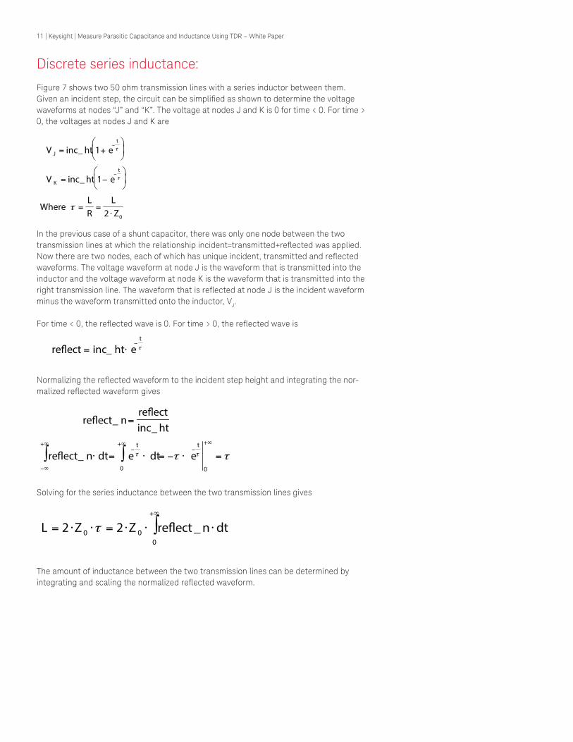
Figure 7 shows two 50 ohm transmission lines with a series inductor between them. Given an incident step, the circuit can be simplified as shown to determine the voltage waveforms at nodes “J” and “K”. The voltage at nodes J and K is 0 for time < 0. For time > 0, the voltages at nodes J and K are
In the previous case of a shunt capacitor, there was only one node between the two transmission lines at which the relationship incident=transmitted+reflected was applied.Now there are two nodes, each of which has unique incident, transmitted and reflectedwaveforms. The voltage waveform at node J is the waveform that is transmitted into theinductor and the voltage waveform at node K is the waveform that is transmitted into the right transmission line. The waveform that is reflected at node J is the incident waveformminus the waveform transmitted onto the inductor, VJ.
For time < 0, the reflected wave is 0. For time > 0, the reflected wave is
Normalizing the reflected waveform to the incident step height and integrating the nor-malized reflected waveform gives
Solving for the series inductance between the two transmission lines gives
The amount of inductance between the two transmission lines can be determined by integrating and scaling the normalized reflected waveform.
V
V
Where
J
K
= +
= −
= =⋅
−
−
inc ht e
inc ht e
LR
LZ
t
t
_
_
1
1
2 0
τ
τ
τ
re�ect inc ht et
= ⋅−
_ τ
re�ect nre�ectinc ht
re�ect n dt e dt et t
__
_
=
⋅ = ⋅ = − ⋅ =−
+∞
−∞
+∞−
+∞
τ ττ τ0 0
L Z Z re�ect n dt= ⋅ ⋅ = ⋅ ⋅ ⋅+∞
2 20 00
τ _

12 | Keysight | Measure Parasitic Capacitance and Inductance Using TDR – White Paper
Figure 7
13 | Keysight | Measure Parasitic Capacitance and Inductance Using TDR – White Paper
Figure 8

14 | Keysight | Measure Parasitic Capacitance and Inductance Using TDR – White Paper
Excess series inductance:
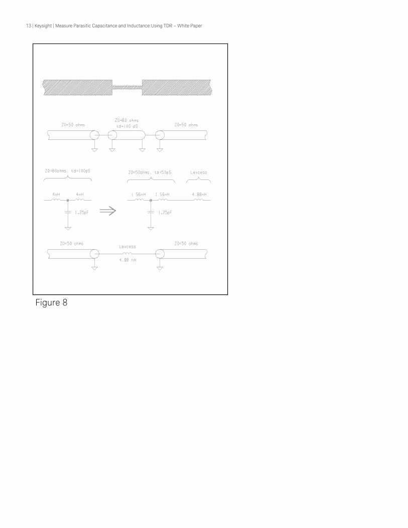
In the previous two cases of shunt capacitance and series inductance, the discontinuity was caused by discrete, lumped capacitance or inductance. Discontinuities can alsobe caused by distributed shunt capacitance and series inductance. Consider the PC board traces shown in figure 8. Being over a ground plane, the traces form microstriptransmission lines. The circuit can be modeled as two long, 1 nS, 50 ohm transmission lines separated by a short , 100 pS, 80 ohm transmission line. Modeling the discontinuityas a short, high impedance transmission line produces accurate simulations up to very high frequencies, or for incident waveforms with very fast transitions.
The discontinuity can also be modeled as a single discrete inductor. Modeling the discon-tinuity as an inductor produces less accurate simulations at high frequencies, but, when transition times are much larger than the time delay of the discontinuity, a simple inductorproduces accurate simulation results. The simpler model provides quick insight to the be-havior of the circuit. To say a discontinuity looks like 4.9 nH of series inductance provides most people with more insight than to say it looks like a 100 pS long, 80 ohm transition line. Also, simulating a single inductor is much faster than simulating a very short transmission line.
The total series inductance of the 100 pS long, 80 ohm transmission line is
To model the short trace as an 8 nH inductor would be incorrect because the trace also has shunt capacitance. The total shunt capacitance of the trace is
To simplify the model of the discontinuity, separate the total series inductance into two parts. One part is the amount of inductance that would combine with the total capac-itance to make a section of 50 ohm transmission line, or to “balance” the total capaci-tance . The remaining part is the amount of inductance that is in excess of the amount necessary to balance the total capacitance. Now, combine the total capacitance with the portion of total inductance that balances that capacitance and make a short section of 50 ohm transmission line. Put this section of transmission line in series with the remaining, or excess, inductance. The short 50 ohm transmission line does nothing except increase the time delay between the source and load. The excess inductance (not the total inductance) causes an incident wave to generate a nonzero reflected wave and a non-identical trans-mitted wave. This is the correct amount of inductance to model the short, narrow trace as.
In this case, the portion of the total inductance that balances the total capacitance is
and the remaining, excess inductance is
L t Z pS ohms nHTotal d High= ⋅ = ⋅ =100 80 8
Ct
ZpS
ohmspFTotal
d
High
= = =10080
125.
L L L nH nH nHExcess Total Balance= − = − =8 3.125 4 . 875
15 | Keysight | Measure Parasitic Capacitance and Inductance Using TDR – White Paper
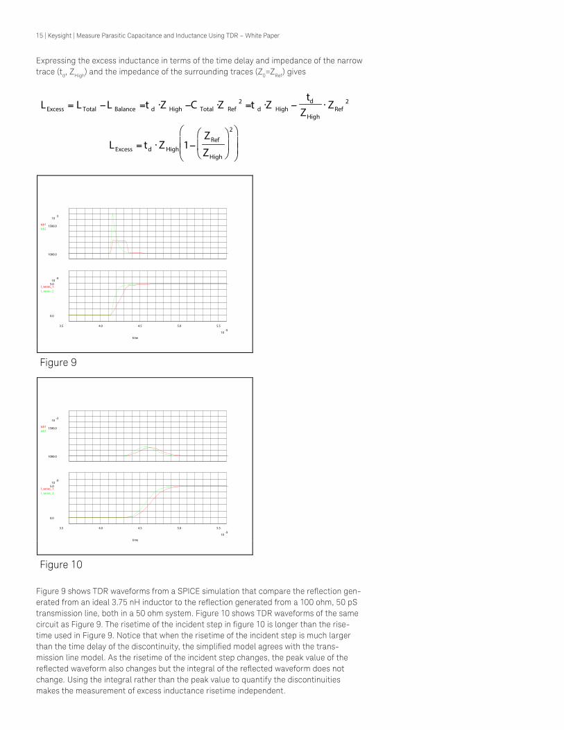
Expressing the excess inductance in terms of the time delay and impedance of the narrow trace (td, ZHigh) and the impedance of the surrounding traces (Z0=ZRef) gives
L L L t Z C Z t Zt
ZZ
L t ZZ
Z
Excess Total Balance d High Total Ref d Highd
HighRef
Excess d HighRef
High
= − = ⋅ − ⋅ = ⋅ − ⋅
= ⋅ −
22
2
1
Figure 9 shows TDR waveforms from a SPICE simulation that compare the reflection gen-erated from an ideal 3.75 nH inductor to the reflection generated from a 100 ohm, 50 pStransmission line, both in a 50 ohm system. Figure 10 shows TDR waveforms of the same circuit as Figure 9. The risetime of the incident step in figure 10 is longer than the rise-time used in Figure 9. Notice that when the risetime of the incident step is much larger than the time delay of the discontinuity, the simplified model agrees with the trans-mission line model. As the risetime of the incident step changes, the peak value of the reflected waveform also changes but the integral of the reflected waveform does notchange. Using the integral rather than the peak value to quantify the discontinuities makes the measurement of excess inductance risetime independent.
time
1000.0
1500.0
10-3
3.5 4.0 4.5 5.0 5.5
10-9
0.0
5.010
-9
tdr1tdr2
l_series_1l_series_2
Figure 9
time
1000.0
1500.0
10-3
3.5 4.0 4.5 5.0 5.5
10-9
0.0
5.010
-9
tdr1tdr2
l_series_1l_series_2
Figure 10

16 | Keysight | Measure Parasitic Capacitance and Inductance Using TDR – White Paper
Excess shunt capacitance:
In the example shown, the discontinuity is a section of trace that is narrower than the surrounding traces, hence the discontinuity can be modeled as an inductor. If a discon-tinuity is a section of trace that is wider than the surrounding traces, the discontinuity can be modeled as a capacitor. As in the previous case, the correct value of capaci-tance is not the total capacitance of the wide section of trace but rather the difference between the total capacitance and the portion of that capacitance that combines with the total inductance to make a section of transmission line of the same impedance as the surrounding, reference impedance. In terms of the time delay and impedance of the wide trace (td, ZLow) and the impedance of the surrounding traces (Z0=ZRef), the excess capacitance is
The length of the transmission line to the right of the discontinuity has no effect on the reflected or transmitted waveforms since it is terminated in its characteristic impedance. It has been shown as a long transmission line in order to easily view the transmitted wave. If the right transmission line is removed then the discontinuity is at the termination of the left transmission line. Quantifying parasitic inductance and capacitance at the termination of a transmission line is no different than quantifying parasitic inductance and capacitance along a transmission line.
Non 50 ohm ZRef:Often, the impedance of the system to be measured is not the same as the impedance of the TDR/oscilloscope system. There are two ways to deal with non-50 ohm systems. In one case the TDR can be connected directly to the system to be measured. In the other case an impedance matching network can be inserted between the TDR and the system to be measured. In either case, the above relationships can be applied if corrections are made to the TDR waveform.
Figure 11
CtZ
ZZExcess
d
Ref
Low
Ref
= ⋅ −1
2

17 | Keysight | Measure Parasitic Capacitance and Inductance Using TDR – White Paper
Connecting the TDR directly to a non-50 ohm system creates a system with two discon-tinuities, one being the transition between the 50 ohm TDR and the non-50 ohm system and the other being the discontinuity to be measured. The incident step will change am-plitude at the non-50 ohm interface prior to arriving at the discontinuity to be measured.The reflected wave from the discontinuity creates another reflection when it arrives at the non-50 ohm to 50 ohm interface. This re-reflection propagates back into the non-50 ohm system and generates another reflection when it arrives at the discontinuity being measured. If twice the time delay of the transmission line between the non-50ohm interface and the discontinuity being measured is larger than the settling time of the first reflected wave, then the integral of the normalized reflected wave can be evaluated before any re-reflections arrive. Otherwise, all of the re-reflections must settle before the integral can be evaluated. If the discontinuity is purely capacitive or inductive, then the re-reflections will not change the final value that the integral converges to.
There are two corrections that need to be made to the TDR waveform. First, the height of the step that is incident to the discontinuity, inc_ht, is not the same height as the height of the step that was generated by the TDR, tdr_ht. Second, the reflected waveform that is viewed by the oscilloscope, reflect_scope, has a different magnitude than the wave-form that was reflected from the discontinuity, reflect. The relationships between the characteristic impedance of the system being measured, the characteristic impedance of the TDR, and the above waveforms are
The characteristic impedance of the system being measured can be calculated from the height of the step reflected from the transition between the 50 ohm TDR system and the non-50 ohm (ZRef) system.
To calculate series inductance or shunt capacitance, the integral of the waveform reflected from the discontinuity, normalized to the height of the step incident to the dis-continuity, needs to be evaluated. In terms of the measured TDR waveform, the normal-ized reflected waveform is
inc ht tdr htZ
Z Z
re�ect scope re�ectZ
Z Z
Ref
Ref TDR
TDR
TDR Ref
_ _
_
= ⋅⋅
+
= ⋅⋅+
2
2
Z ZIncident Re�ectIncident Re�ect
ohmstdr ht ref httdr ht ref htRef TDR= ⋅
+−
= ⋅+−
5011
_ __ _
( )re�ect n
re�ectinc ht
re�ect scopeZ Z
Z
tdr htZ
Z Z
re�ect scopetdr ht
Z Z
Z Z
Ref TDR
TDR
Ref
Ref TDR
Ref TDR
Ref TDR
__
_
_
__
= =
⋅+
⋅
⋅⋅
+
= ⋅+
⋅ ⋅
2
2 4
2

18 | Keysight | Measure Parasitic Capacitance and Inductance Using TDR – White Paper
As an example, the shunt capacitance would be
( )C
Zre�ect n
Z Z
Z Zre�ect scope
tdr htRef
Ref TDR
TDR Ref
= − ⋅ ⋅ = −+
⋅ ⋅⋅
+∞+∞22
2
200
_ dt__
dt
Reflections between the discontinuity and the non-50 ohm transition can be removed if an impedance matching network is inserted between the TDR and the non-50 ohm system. Two resistors are the minimum requirement to match an impedance transition in both directions. Attenuation across the matching network needs to be accounted for pri-or to integrating the reflected waveform. When a matching network is used, neither the impedance of the system being tested nor the attenuation of the matching network can be ascertained from the TDR waveform. If tran_12 is the gain of the matching network going from the TDR to the system and tran_21 is the gain going from the system to the TDR, then the normalized reflected waveform is
re�ect nre�ectinc ht
re�ect scopetran
tdr ht tranre�ect scope
tdr ht tran tran_
_
__
_ ___ _ _
= =⋅
= ⋅⋅
2112
112 21
Series Capacitance:
So far, all of the discontinuities that have been measured have been mere perturba-tions in the characteristic impedance of transmission line systems. The discontinuities have been quantified by analyzing the reflected waveforms using TDR. Now consider a situation where a capacitance to be measured is in series with two transmission lines. The series capacitance can be quantified using the transmitted waveform rather than the reflected waveform, or using Time Domain Transmission (TDT). Given an incident step that arrives at the series capacitance at time = 0, the transmitted waveform is 0 for time < 0. For time > 0, the transmitted waveform is
Where
trans inc ht e
R C Z C
t
o
= ⋅
= ⋅ = ⋅ ⋅
−_ τ
τ 2
Note that tau is now 2*Z0 instead of Z0/2. Normalizing the transmitted waveform to theincident step height and integrating the normalized, transmitted waveform gives
trans ntransinc ht
trans n dt e dt et t
__
_
=
⋅ = ⋅ = − ⋅ =−
+∞
−∞
+∞−
+∞
τ ττ τ0 0
Solving for the series capacitance gives
CZ Z
trans no o
=⋅
⋅ =⋅
⋅ ⋅+∞τ
21
2 0
_ dt

19 | Keysight | Measure Parasitic Capacitance and Inductance Using TDR – White Paper
Figure 12
Shunt Inductance:The last topology to be analyzed will be shunt inductance to ground. Given an incident step that arrives at the shunt inductance at time = 0, the transmitted waveform is 0 for time < 0. For time > 0, the transmitted waveform is
Where
trans inc ht e
LR
LZ
LZ
t
o o
= ⋅
= = =⋅
−_ τ
τ
2
2
This is the same transmitted waveform as in the case of series capacitance. Tau is 2*L/Z0 hence the shunt inductance is
LZ Z
trans n dto o= ⋅ = ⋅ ⋅+∞
2 2 0
τ _

20 | Keysight | Measure Parasitic Capacitance and Inductance Using TDR – White Paper
More complex discontinuities:
Consider a circuit where a transmission line is brought to the input of an integrated circuit (IC) and terminated. Looking from the termination into the IC, there is inductance of the lead in series with capacitance of the gate in series with resistance of the channel. A first order approximation of the load that the IC puts on the termination of the trans-mission line is simply a capacitor. The reflected wave can be integrated to calculate the capacitance but will the series inductance and resistance change the measured value? Looking back to figure 5, the current into the shunt capacitor is
I =⋅
⋅ = − ⋅−inc ht
Ze re�ect
Z
t_ 2 2
00
τ
The integral of the reflected wave is directly proportional to the integral of the current into the capacitor. This means that the value of capacitance calculated from integrating the reflected wave is proportional to the total charge on the capacitor. Resistance or in-ductance in series with the shunt capacitor does not change the final value of charge on the capacitor. Hence, these elements do not change the measured value of capacitance. Series resistance decreases the height and increases the settling time of the reflected wave. Series inductance superimposes ringing onto the reflected waveform.Neither changes the final value of the integral of the reflected wave. Note that induc-tance in series with the transmission line, as apposed to inductance in series with the capacitor, will change the measured value of capacitance. Similarly, resistance or capacitance in parallel with a series inductance do not change the measured value of inductance.
Now consider a situation where a voltage probe is used to measure signals on PC board traces. What affect does the probe have on signals that are propagating along the traces? To a first order, the load of a “high impedance” probe will be capacitive and the value of capacitance can be measured by integrating the reflected wave. However, some passive probes that are optimized for bandwidth can also have a significant resistive load (these probes usually have a much lower capacitive load than the “high impedance” probes). Looking at the reflected wave in figure 14, the resistive load of the probe intro-duces a level shift at 4 nS. The level shift adds a ramp to the integral hence the integral
Figure 14

21 | Keysight | Measure Parasitic Capacitance and Inductance Using TDR – White Paper
never converges on a final value. To measure the value of capacitance, the integral can be evaluated at two different times after the reflected wave has settled to its final value,say at 6 and 7 nS. Since the reflected wave has settled, the difference between the twovalues is due only to the level shift. The component of the integral due to the levelshift can be removed from the total integral by subtracting twice the difference between 6 and 7 nS from the value at 6 nS. The remaining component of the integral is due to the shunt capacitance.
There are many instances where discontinuities in transmission line systems are unavoid-able. The effects of an unavoidable discontinuity can be minimized by introducing dis-continuities of opposite polarity as close as possible to the unavoidable discontinuity. For example, if the narrow part of the trace shown in figure 8 is required, then the traces oneither side of the narrow trace can be made wider to compensate for the excess induc-tance of the trace. The amount of excess capacitance required to compensate the 4.88 nH of excess inductance is Z0
2*L = (50 ohm)2*4.88 nH = 1.95 pF. If the widest trace that can be added has a characteristic impedance of 30 ohms, then 152 pS of this trace will add 1.95 pF of excess capacitance. Propagation delays on typical PC board traces are around 150 pS/inch hence adding .5 inches of 30 ohm transmission line on each side of the narrow trace will balance the excess inductance of the trace. Balancing the dis-continuity reduces reflections and makes the transmitted wave more closely resemble the incident wave. A discontinuity that is balanced will produce a reflected wave whose integral is zero. In this case, the integral of the reflected wave can be used to determine how well a discontinuity is balanced.
22 | Keysight | Measure Parasitic Capacitance and Inductance Using TDR – White Paper
Summary:
TDR can be used to very accurately measure impedances and discontinuities in trans-mission line systems. To build the most accurate models, all of the information contained in the reflected or transmitted waveforms must be used. Very accurate models can be fairly cumbersome to assemble and use since they can contain many discrete compo-nents or many sections of very short transmission lines. Hewlett Packard and Tektronics both offer oscilloscopes with TDR that have step generators with < 35 pS risetimes. Reflections from a 35 pS incident wave contain information to 10 gigaHertz (GHz) of bandwidth hence these TDRs can be used to build models that are accurate to 10 GHz.
Typical high speed digital drivers produce risetimes around 1 nS. The fastest drivers produce risetimes around 300 pS. Building a model that is accurate with 35 pS rise-times to be used in a system containing 350 pS risetimes is probably going above and beyond the call of duty. When a model only needs to be accurate over a lower range of frequencies, say to 2 GHz, then a simplified model may be all that is required. Integrating the reflected wave to determine excess inductance or capacitance combines everything in the discontinuity into a single element. The calculated element value is the correct value for a low frequency model. If, for example, the discontinuity is inductive and then capacitive, then a single element model will be less accurate at higher frequencies. If a discontinuity is mainly capacitive, then a single element model will be accurate even at higher frequencies.
Hewlett Packard recently introduced the HP54750A oscilloscope and the HP54754A TDR plug-in. All of the measurements discussed above can be made by positioning two cursors on the TDR or TDT waveform. The oscilloscope calculates the integral of the normalized reflected or transmitted waveform and displays the appropriate value of inductance or capacitance. Parasitic inductances and capacitances can be accurately quantified in the time it takes to position two cursors.

23 | Keysight | Measure Parasitic Capacitance and Inductance Using TDR – White Paper
This information is subject to change without notice.© Keysight Technologies, 2017Published in USA, December 1, 20175988-6505ENwww.keysight.com
www.keysight.com/find/lightwave
For more information on Keysight Technologies’ products, applications or services, please contact your local Keysight office. The complete list is available at:www.keysight.com/find/contactus
Americas Canada (877) 894 4414Brazil 55 11 3351 7010Mexico 001 800 254 2440United States (800) 829 4444
Asia PacificAustralia 1 800 629 485China 800 810 0189Hong Kong 800 938 693India 1 800 11 2626Japan 0120 (421) 345Korea 080 769 0800Malaysia 1 800 888 848Singapore 1 800 375 8100Taiwan 0800 047 866Other AP Countries (65) 6375 8100
Europe & Middle EastAustria 0800 001122Belgium 0800 58580Finland 0800 523252France 0805 980333Germany 0800 6270999Ireland 1800 832700Israel 1 809 343051Italy 800 599100Luxembourg +32 800 58580Netherlands 0800 0233200Russia 8800 5009286Spain 800 000154Sweden 0200 882255Switzerland 0800 805353
Opt. 1 (DE)Opt. 2 (FR)Opt. 3 (IT)
United Kingdom 0800 0260637
For other unlisted countries:www.keysight.com/find/contactus(BP-9-7-17)
DEKRA CertifiedISO9001 Quality Management System
www.keysight.com/go/qualityKeysight Technologies, Inc.DEKRA Certified ISO 9001:2015Quality Management System
Evolving Since 1939Our unique combination of hardware, software, services, and people can help you reach your next breakthrough. We are unlocking the future of technology. From Hewlett-Packard to Agilent to Keysight.
myKeysightwww.keysight.com/find/mykeysightA personalized view into the information most relevant to you.
http://www.keysight.com/find/emt_product_registrationRegister your products to get up-to-date product information and find warranty information.
Keysight Serviceswww.keysight.com/find/serviceKeysight Services can help from acquisition to renewal across your instrument’s lifecycle. Our comprehensive service offerings—one-stop calibration, repair, asset management, technology refresh, consulting, training and more—helps you improve product quality and lower costs.
Keysight Assurance Planswww.keysight.com/find/AssurancePlansUp to ten years of protection and no budgetary surprises to ensure your instruments are operating to specification, so you can rely on accurate measurements.
Keysight Channel Partnerswww.keysight.com/find/channelpartnersGet the best of both worlds: Keysight’s measurement expertise and product breadth, combined with channel partner convenience.