keysight technologies vector signal analysis...
TRANSCRIPT

Keysight Technologies Vector Signal Analysis Basics
Application Note

ADC Time
Anti-alias filter Quadrature
detector,digital filtering
FFT
IFinput
Localoscilator
RFinput
Time domain
Frequency domain
Modulation domain
Code domain
t
f
I
Q
0 code 15
I
Q
Demod-ulator
90 degs
t t
Analog data Digitized data stream
Digital IF andDSP techniques
LO
Figure 1-1. The vector signal analyzer digitizes the analog input signal and uses DSP technology to process and provide data outputs; the FFT algorithm produces frequency domain results, the demodulator algorithms produce modulation and code domain results
02 | Keysight | Vector Signal Analysis Basics - Application Note
This application note serves as a primer on the vector signal analyzer (VSA). This chapter discusses VSA measurement concepts and theory of operation; Chapter 2 discusses VSA vector-modulation analysis and, specifically, digital-modulation analysis.
Analog, swept-tuned spectrum analyzers use superheterodyne technology to cover wide frequency ranges; from audio, through microwave, to millimeter frequencies. Fast Fourier transform (FFT) analyzers use digital signal processing (DSP) to provide high-resolution spectrum and network analysis, but are limited to low frequencies due to the limits of analog-to-digital conversion (ADC) and signal processing technologies. Today’s wide-bandwidth, vector-modulated (also called complex or digitally modulated), time-varying signals benefit greatly from the capabilities of FFT analysis and other DSP techniques. VSAs combine superheterodyne technology with high speed ADCs and other DSP technologies to offer fast, high-resolution spectrum measurements, demodulation, and advanced time-domain analysis. A VSA is especially useful for characterizing complex signals such as burst, transient, or modulated signals used in communications, video, broadcast, sonar, and ultrasound imaging applications.
Figure 1-1 shows a simplified block diagram of a VSA analyzer. The VSA implements a very different measurement approach than traditional swept analyzers; the analog IF section is replaced by a digital IF section incorporating FFT technology and digital signal processing. The traditional swept-tuned spectrum analyzer is an analog system; the VSA is fundamentally a digital system that uses digital data and mathematical algorithms toperform data analysis. For example, most traditional hardware functions, such as mixing, filtering, and demodulation, are accomplished digitally, as are many measurement operations. The FFT algorithm is used for spectrum analysis, and the demodulator algorithms are used for vector analysis applications.
Chapter 1Vector Signal Analyzer

t0
Display shows fullspectral display
A
ff1 f2
Simulated parallel-filter processing
Time domain
Vector analysis
Fourier analysis Frequency domain
Time record
Frequencyresolutionbandwidth IF filter
Swept analysis
Carrier
Sweep spanStart frequency Stop frequency
f
Time sampled dataA
Frequency spectrum
Figure 1-2. Swept-tuned analysis displays the instantaneous time response of a narrowband IF filter to the input signal. Vector analysis uses FFT analysis to transform a set of time domain samples into frequency domain spectra.
03 | Keysight | Vector Signal Analysis Basics - Application Note
A significant characteristic of the VSA is that it is designed to measure and manipulate complex data. In fact, it is called a vector signal analyzer because it has the ability to vector detect an input signal (measure the magnitude and phase of the input signal). You will learn about vector modulation and detection in Chapter 2. It is basically a measurement receiver with system architecture that is analogous to, but not identical to, a digital communications receiver. Though similar to an FFT analyzer, VSAs cover RF and microwave ranges, plus additional modulation-domain analysis capability. These advancements are made possible through digital technologies such as analog-to-digital conversion and DSP that include digital intermediate frequency (IF) techniques and fast Fourier transform (FFT) analysis.
Because the signals that people must analyze are growing more complex, the latest generations of spectrum analyzers have moved to a digital architecture and often include many of the vector signal analysis capabilities previously found only in VSAs. Some analyzers digitize the signal at the instrument input, after some amplification, or after one or more downconverter stages. In any of these cases, phase as well as magnitude is preserved in order to perform true vector measurements. Capabilities are then determined by the digital signal processing capability inherent in the spectrum analyzer firmware or available as add-on software running either internally (measurement personalities) or externally (vector signal analysis software) on a computer connected to the analyzer.
VSA measurement advantages
Vector analysis measures dynamic signals and produces complex data results The VSA offers some distinct advantages over analog swept-tuned analysis. One of the major advantages of the VSA is its ability to better measure dynamic signals. Dynamic signals generally fall into one of two categories: time-varying or complex modulated. Time-varying are signals whose measured properties change during a measurement sweep (such as burst, gated, pulsed, or transient). Complex-modulated signals cannot be solely described in terms of simple AM, FM, or PM modulation, and include most of those used in digital communications, such as quadrature amplitude modulation (QAM).
Vector Signal Analyzer(continued)
04 | Keysight | Vector Signal Analysis Basics - Application Note
A traditional swept-spectrum analyzer1, in effect, sweeps a narrowband filter across a range of frequencies, sequentially measuring one frequency at a time. Unfortunately, sweeping the input works well for stable or repetitive signals, but will not accurately represent signals that change during the sweep. Also, this technique only provides scalar (magnitude only) information, though some other signal characteristics can be derived by further analysis of spectrum measurements.
The VSA measurement process simulates a parallel bank of filters and overcomes swept limitations by taking a “snapshot,” or time-record, of the signal; then processing all frequencies simultaneously. For example, if the input is a transient signal, the entire signal event is captured (meaning all aspects of the signal at that moment in time are digitized and captured); then used by the FFT to compute the “instantaneous” complex spectra versus frequency. This process can be performed in real-time, that is, without missing any part of the input signal. For these reasons, the VSA is sometimes referred to as a “dynamic signal analyzer” or a “real-time signal analyzer”. The VSA’s ability to track a fast-changing signal isn’t unlimited, however; it depends on the VSA’s computational capability.
The VSA decreases measurement timeParallel processing yields another potential advantage for high-resolution (narrow resolution bandwidth) measurements; faster measurement time. If you’ve used a swept-tuned spectrum analyzer before, you already know that narrow resolution bandwidth (RBW) measurements of small frequency spans can be very time-consuming. Swept-tuned analyzers sweep frequencies from point to point slowly enough to allow the analog resolution bandwidth filters to settle. By contrast, the VSA measures across the entire frequency span at one time. However, there is analogous VSA settling time due to thedigital filters and DSP. This means the VSA sweep speed is limited by data collection and digital processing time rather than analog filters. But this time is usually negligible when compared to the settling time of analog filters. For certain narrow bandwidth measurements, the VSA can complete a measurement up to 1000 times faster than conventional swept-tuned analyzers.
In a swept-tuned spectrum analyzer, the physical bandwidth of the sweeping filter limits the frequency resolution. The VSA doesn’t have this limitation. Some VSAs can resolve signals that are spaced less than 100 μHz apart. Typically, VSA resolution is limited by source and analyzer frequency stability, as well as by the amount of time you are willing to devote to the measurement. Increasing the resolution also increases the time it takes to measure the signal (the length of the required time-record).
Time-capture is a great tool for signal analysis and troubleshooting Another feature that is extremely useful is the time-capture capability. This allows you to record actual signals in their entirety without gaps, and replay them later for any type of data analysis. The full set of measurement features can be applied to the captured signal. For example, you could capture a transmitted digital communications signal and then perform both spectrum and vector-modulation analysis to measure signal qualityor identify signal impairments.
Vector Signal Analyzer(continued)
1. For more information on spectrum analyzers, see Keysight Application Note 150, Spectrum Analysis Basics, literature number 5952-0292.
DSP provides multi-domain measurements in one instrumentThe use of digital signal processing (DSP) also yields additional benefits; it provides time, frequency, modulation, and code domain measurement analysis in one instrument. Having these capabilities increases the analyzer’s value to you and improves the quality of your measurements. FFT analysis allows easy and accurate views of both time and frequency domain data. The DSP provides vector modulation analysis, including both analog and digital modulation analysis. The analog demodulator produces AM, FM and PM demodulation results, similar to that of a modulation analyzer, allowing you to view amplitude, frequency, and phase profiles versus time. The digital demodulator performs a broad range of measurements on many digital communications standards (such as W-CDMA, GSM, cdma2000, and more) and produces many useful measurement displays and signal-quality data.
Although the VSA clearly provides important benefits, the conventional analog swept-tuned analyzers can provide higher frequency coverage and increased dynamic range capability.
VSA measurement concepts and theory of operationAs mentioned earlier, the VSA is fundamentally a digital system that uses DSP to perform spectrum analysis with FFTs, and uses demodulator algorithms to perform vector-modulation analysis. You may recall from Fourier analysis, that the FFT is a mathematical algorithm that operates on time-sampled data and provides time-to-frequency domain transformations. The analog signal must be digitized in the time-domain, then the FFT algorithm executes to compute the spectra. Conceptually, the VSA implementation is simple and straightforward: digitize the input signal, then compute the measurement results. See Figure 1-3. However, in practice, there are many factors that must be accounted for in order for the measurement to be meaningful and accurate. (For more information about FFT analysis, refer to the References section at the end of this application note.)
....
......... .. . .. ....
... ....
.. .ADC FFT
Time recordSampler andA/D converter
Frequency spectrum
1 kHz sine wave Digitzed 1kHz sine wave
1 kHzf
Fast Fourier transform(FFT) processing
t
1 kHz spectrum
t
Figure 1-3. 1 kHz FFT analysis example: digitize time-domain signal and use FFT analysis to convert it to the frequency domain
05 | Keysight | Vector Signal Analysis Basics - Application Note
Vector Signal Analyzer(continued)
If you are familiar with FFT analysis, you already know the FFT algorithm makes several assumptions about the signal it is processing. The algorithm doesn’t check to verify the validity of these assumptions for a given input, and it will produce invalid results, unless you or the instrument validates the assumptions. Fortunately, as you will learn in the following discussion, the Keysight Technologies, Inc. VSA implementation was designed with FFT-based analysis in mind. It has many integrated features to eliminate potential error sources, plus enhancements that provide swept-tuned usability in an FFT-based analyzer.
Figure 1-4 illustrates a general system block diagram of a VSA analyzer. Different manufacturers might use slightly different designs and, through DSP, many of the functions could occur at different places. Figure 1-4 shows a generalized diagram of the technique that Keysight uses in its VSAs. The VSA spectrum analysis measurement process includes these fundamental stages:
1. Signal conditioning with frequency translation 2. Analog-to-digital conversion 3. Quadrature detection 4. Digital filtering and resampling 5. Data windowing 6. FFT analysis (for vector modulation, blocks 5 and 6 are replaced with the demodulator block)
The first stage of the measurement process is called signal conditioning. This stage includes several important functions that condition and optimize the signal for the analog-to-digital conversion and FFT analysis. The first function is AC and DC coupling. This option is necessary if you need to remove unwanted DC biases in the measurement setup. Next, the signal is either amplified or attenuated for optimal signal level into the mixer. The mixer stage provides frequency translation, or RF-to-IF downconversion, and mixes the signal down to the final IF. This operation is the same as the superheterodyne function of the swept-tuned analyzer and extends FFT analysis capabilities through microwave. In practice, it may take several downconversion stages to reach the final IF frequency. Some analyzers provide external IF input capability; by providing your own IF, you can extend the upper frequency range of the analyzer to match a receiver you provide.
ADC
Sam
pled
tim
eda
taAnti-aliasfilter Quadrature
detector
FFT
Localoscilator
RFinput
Demodulator
DSPtechniques
IF
Samplememory
Digitaldecimating
filters
Display
"Vector modulation analysis"
"Spectrum analysis"
Note: Actual VSA implementation may be different.
Digital LO
Res
ampl
ing
(arb
itary
spa
ns)
Window
Time-domain
Freq
-dom
ain
Mod
ulat
ion-
dom
ain
Code
-dom
ain
Hardwareimplementation
IFAttenuationAC/DC couplinggain amplifiers
Tim
e da
taco
rrec
tions
Mixer
1 2 3 4 5 6
Signal conditioning
90 degs
Q
I
Figure 1-4. Vector signal analyzer simplified block diagram
Vector Signal Analyzer(continued)
06 | Keysight | Vector Signal Analysis Basics - Application Note
The final stage of the signal conditioning process is extremely important to a sampled system and FFT analysis; signal alias protection. The anti-alias filter performs this function. An analyzer that does not have adequate protection from aliasing may show frequency components that are not part of the original signal. The sampling theorem states that if the signal is sampled at a rate greater than 2 times the highest significant frequency component present in the signal, the sampled signal can be reconstructed exactly. The minimum acceptable sample rate is called the Nyquist rate. Thus,
fs > 2 (fmax)
where fs = sample rate fmax = highest frequency component
If the sampling theorem is violated, “aliasing” error products can result. Therefore, to prevent alias products for a given maximum frequency, there must not be significant signal energy above 1/2 the sample rate. Figure 1-5 shows a set of sample points, which fit two different waveforms. The higher-frequency waveform violates the sampling theorem. Unless an anti-alias filter is used, the two frequencies will be indistinguishable when processed digitally.
To prevent aliasing, two conditions must be satisfied:1. The input signal to the digitizer/sampler must be band limited. In other words, there must exist a maximum frequency ( fmax) above which no frequency components are present. 2. The input signal must be sampled at a rate that satisfies the sampling theorem.
The solution to the aliasing problem seems simple enough. First you select the maximum frequency ( fmax) that the analyzer will measure, then make sure the sampling frequency ( fs) is twice that frequency. This step satisfies condition number 2 and makes sure that the analyzer can accurately measure the frequencies of interest. Next you insert a low-pass filter (an anti-aliasing filter) to remove all fr quencies above fmax, thus ensuring that the measurement will exclude all frequencies except those you are interested in. This step satisfies condition number 1 and makes sure the signal is band limited.
Reconstructed "alias" signal Actualsignal
ADC samplepoints
f sf f
X(f)
f
(a) Aliasing in the time-domain (b) Aliasing in the frequency-domain
Unwanted frequency components arefolded onto the spectrum below cutoff.
recovered aliasspectrum followsdashed line.
fs0
( /2)f s
Figure 1-5. Aliasing products occur when the signal is undersampled. Undesirable frequencies appear under the alias of another (baseband) frequency
Vector Signal Analyzer(continued)
07 | Keysight | Vector Signal Analysis Basics - Application Note

There are two factors that complicate this simple anti-aliasing solution. The first, and easiest to address, is that the anti-alias filter has a finite roll off rate. As shown in figure 1-6, there is a transition band in practical filters between the passband and stopband. Frequencies within the transition band could produce alias frequencies. To avoid these alias products, the filter cutoff must be below the theoretical upper frequency limit of fs divided by 2. An easy solution to this problem is to oversample (sample above the Nyquist rate). Make the sampling frequency slightly above 2 times fmax so that it is twice the frequency at which the stopband actually starts, not twice the frequency you are trying to measure. Many VSA implementations use a guard band to protect against displaying aliased frequency components. The FFT computes the spectral components out to 50% of fs (equivalently fs/2). A guard band, between approximately 40% to 50% of fs (or fs/2.56 to fs/2), is not displayed because it may be corrupted by alias components. However, when the analyzer computes the inverse FFT, the signals in the guard band are used to provide the most accurate time-domain results. The high-roll-off-rate filter, combined with the guard band, suppresses potential aliasing components, attenuating them well below the noise floor of the analyzer.
The second complicating factor in alias protection (limited frequency resolution) is much harder to solve. First, an anti-alias filter that is designed for wide frequency spans (high sample rates) is not practical for measuring small resolution bandwidths for two reasons; it will require a substantial sample size (memory allocation) and a prohibitively large number of FFT computations (long measurement times). For example, at a 10 MHz sample rate, a 10 Hz resolution bandwidth measurement would require more than a 1 million point FFT, which translates into large memory usage and a long measurement time. This is unacceptable because the ability to measure small resolution bandwidths is one of the main advantages of the VSA.
One way of increasing the frequency resolution is by reducing fs, but this is at the expense of reducing the upper-frequency limit of the FFT and ultimately the analyzer bandwidth. However, this is still a good approach because it allows you to have control over the resolution and frequency range of the analyzer. As the sample rate is lowered, the cut-off frequency of the anti-alias filter must also be lowered, otherwise aliasing will occur. One possible solution would be to provide an anti-aliasing filter for every span, or a filter with selectable cutoff frequencies. Implementing this scheme with analog filters would be difficult and cost prohibitive, but it is possible to add additional anti-alias filters digitally through DSP.
Band limited
analog signalADC
Wideband
input signal
Guard band
fs / 2.56
Passband Transition Stopband
Anti-alias filter
( ) fs / 2( )f
Figure 1-6. The anti-alias filter attenuates signals above fs/2. A guard band between 40% to 50% of fs is not displayed
Vector Signal Analyzer(continued)
08 | Keysight | Vector Signal Analysis Basics - Application Note

Digital decimating filters and resampling algorithms provide the solution to the limited frequency resolution problem, and it is the solution used in Keysight VSAs. Digital decimating filters and resampling perform the operations necessary to allow variable spans and resolution bandwidths. The digital decimating filters simultaneously decrease the sample rate and limit the bandwidth of the signal (providing alias protection). The sample rate into the digital filter is fs; the sample rate out of the filter is fs/n, where “n” is the decimation factor and an integer value. Similarly, the bandwidth at the input filter is “BW,” and the bandwidth at the output of the filter is “BW/n”. Many implementations perform binary decimation (divide-by-2 sample rate reduction), which means that the sample rate is changed by integer powers of 2, in 1/(2n) steps (1/2, 1/4, 1/8...etc). Frequency spans that result from “divide by 2n” are called cardinal spans.Measurements performed at cardinal spans are typically faster than measurements performed at arbitrary spans due to reduced DSP operations.
The decimating filters allow the sample rate and span to be changed by powers of two. To obtain an arbitrary span, the sample rate must be made infinitely adjustable. This is done by means of a resampling or interpolation filter, which follows the decimation filters. For more details regarding resampling and interpolation algorithms, refer to the References section at the end of this application note.
Even though the digital and resampling filters provide alias protection while reducing the sample rate, the analog anti-alias filter is still required, since the digital and resampling filters are, themselves, a sampled system which must be protected from aliasing. The analog anti-alias filter protects the analyzer at its widest frequency span with operation at fs. The digital filters follow the analog filter and provide anti-alias protection for the narrower, user-specified spans.
The next complication that limits the ability to analyze small resolution bandwidths is caused by a fundamental property of the FFT algorithm itself; the FFT is inherently a baseband transform. This means that the frequency range of the FFT starts from 0 Hz (or DC) and extends to some maximum frequency, fs divided by 2. This can be a significant limitation in measurement situations where a small frequency band needs to be analyzed. For example, if an analyzer has a sample rate of 10 MHz, the frequency range would be 0 Hz to 5 MHz ( fs/2). If the number of time samples (N) were 1024, the frequency resolution would be 9.8 kHz ( fs/N). This means that frequencies closer than 9.8 kHz could not be resolved.
As just mentioned, you can control the frequency span by varying the sample rate, but the resolution is still limited because the start frequency of the span is DC. The frequency resolution can be arbitrarily improved, but at the expense of a reduced maximum frequency. The solution to these limitations is a process called band selectable analysis, also known as zoom operation or zoom mode. Zoom operation allows you to reduce the frequency span while maintaining a constant center frequency. This is very useful because it allows you to analyze and view small frequency components away from 0 Hz. Zooming allows you to focus the measurement anywhere within the analyzers frequency range (Figure 1-7).
Vector Signal Analyzer(continued)
09 | Keysight | Vector Signal Analysis Basics - Application Note

Zoom operation is a process of digital quadrature mixing, digital filtering, and decimat-ing/resampling. The frequency span of interest is mixed with a complex sinusoid at the zoom span center frequency ( fz), which causes that frequency span to be mixed down to baseband. The signals are filtered and decimated/resampled for the specified span, all out-of-band frequencies removed. This is the band-converted signal at IF (or base-band) and is sometimes referred to as “zoom time” or “IF time”. That is, it is the time-domain representation of a signal as it would appear in the IF section of a receiver. Zoom measurements are discussed further in the “Time-domain display” section near the end of this chapter.
Sample memoryThe output of the digital decimating filters represents a bandlimited, digital version of the analog input signal in time-domain. This digital data stream is captured in sample memory (Figure 1-4). The sample memory is a circular FIFO (first in, first out) buffer that collects individual data samples into blocks of data called time records, to be used by the DSP for further data processing. The amount of time required to fill the time record is analogous to the initial settling time in a parallel-filter analyzer. The time data col-lected in sample memory is the fundamental data used to produce all measurement results, whether in the frequency domain, time domain, or modulation domain.
Time domain data correctionsTo provide more accurate data results, many VSAs implement time data correction capability through an equalization filter. In vector analysis, the accuracy of the time data is very important. Not only is it the basis for all of the demodulation measure-ments, but it is also used directly for measurements such as instantaneous power as a function of time. Correcting the time data is the last step in creating a nearly ideal ban-dlimiting signal path. While the digital filters and resampling algorithms provide for arbitrary bandwidths (sample rates and spans), the time-domain corrections determine the final passband characteristic of the signal path. Time-domain corrections would be unnecessary if the analog and digital signal paths could be made ideal. Time-domain corrections function as an equalization filter to compensate for passband imperfections. These imperfections come from many sources. The IF filters in the RF section, the analog anti-aliasing filter, the decimating filters, and the resampling filters all contribute to passband ripple and phase nonlinearities within the selected span.
Broadband time-domain signal
fmax
t
0 Hz
Zoom span
fstopfstart
Time-domainbaseband
Frequency-domain response
Band selectable analysis
(zoom-mode)
(Zoom span center frequency)
0 Hz
fstop–fstart0 Hz
fstopfstart
Spectrum display
(a)
(b)
(d)
(e)
(c)(f)
Analyzer display
Digital LO frequency spectrum at fz
Frequency translated version of the zoom span
fz
fz
fz
fz
Figure 1-7. Band-selectable analysis (or zoom mode): (a) measured broadband signal,(b) spectrum of the measured signal, (c) selected zoom span and center frequency,(d) digital LO spectrum (@ zoom center frequency), (e) frequency span mixed down to baseband,(f) display spectrum annotation is adjusted to show the correct span and center frequency
Vector Signal Analyzer(continued)
10 | Keysight | Vector Signal Analysis Basics - Application Note
The design of the equalization filter begins by extracting information about the analog signal path from the self-calibration data based on the instrument’s configuration. This is the data used to produce the frequency-domain correction output display. Once the analog correction vector has been computed, it is modified to include the effects of the decimating and resampling filters. The final frequency response computations cannot be performed until after you have selected the span, because that determines the number of decimating filter stages and resampling ratio. The composite correction vector serves as the basis for the design of the digital equalization filter that is applied to the time data.
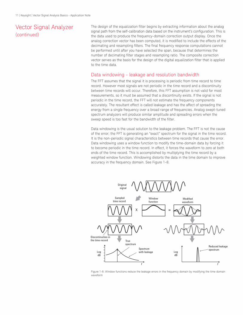
Data windowing - leakage and resolution bandwidth The FFT assumes that the signal it is processing is periodic from time record to time record. However most signals are not periodic in the time record and a discontinuity between time records will occur. Therefore, this FFT assumption is not valid for most measurements, so it must be assumed that a discontinuity exists. If the signal is not periodic in the time record, the FFT will not estimate the frequency components accurately. The resultant effect is called leakage and has the affect of spreading the energy from a single frequency over a broad range of frequencies. Analog swept-tuned spectrum analyzers will produce similar amplitude and spreading errors when the sweep speed is too fast for the bandwidth of the filter.
Data windowing is the usual solution to the leakage problem. The FFT is not the cause of the error; the FFT is generating an “exact” spectrum for the signal in the time record. It is the non-periodic signal characteristics between time records that cause the error. Data windowing uses a window function to modify the time-domain data by forcing it to become periodic in the time record. In effect, it forces the waveform to zero at both ends of the time record. This is accomplished by multiplying the time record by a weighted window function. Windowing distorts the data in the time domain to improve accuracy in the frequency domain. See Figure 1-8.
Discontinuities inthe time-record
Original signal
Sampledtime record
Windowfunction
Modifiedwaveform
Reduced leakagespectrum
Truespectrum
f
Spectrumwith leakage
f
Log dB
Log dB
X =
Figure 1-8. Window functions reduce the leakage errors in the frequency domain by modifying the time domain waveform
Vector Signal Analyzer(continued)
11 | Keysight | Vector Signal Analysis Basics - Application Note

Analyzers automatically select the appropriate window filter based on assumptions of the user’s priorities, derived from the selected measurement type. However, if you want to manually change the window type, VSAs usually have several built-in window types that you can select from. Each window function, and the associated RBW filter shape, offers particular advantages and disadvantages. A particular window type may trade off improved amplitude accuracy and reduced “leakage” at the cost of reduced frequency resolution. Because each window type produces different measurement results (just how different depends on the characteristics of the input signal and how you trigger on it), you should carefully select a window type appropriate for the measurement you are trying to make. Table 1-1 summarizes four common window types and their uses.
The window filter contributes to the resolution bandwidth
In traditional swept-tuned analyzers, the final IF filter determines the resolution bandwidth. In the FFT analyzers, the window type determines the resolution bandwidth filter shape. And the window type, along with the time-record length, determines the width of the resolution bandwidth filter. Therefore, for a given window type, a change in resolution bandwidth will directly affect the time-record length. Conversely, any change to time-record length will cause a change in resolution bandwidth as shown in the following formula:
RBW = normalized ENBW / T
where ENBW = equivalent noise bandwidth RBW = resolution bandwidth T = time-record length
Equivalent noise bandwidth (ENBW) is a figure of merit that compares the window filter to an ideal, rectangular filter. It is the equivalent bandwidth of a rectangular filter that passes the same amount (power) of white noise as the window. Table 1-2 lists the normalized ENBW values for several window types. To compute the ENBW, divide the normalized ENBW by the time-record length. For example, a Hanning window with a 0.5 second time-record length would have an ENBW of 3 Hz (1.5 Hz-s/0.5 s).
Vector Signal Analyzer(continued)
Window type Common uses
Flat Top 3.819 Hz-s
Gaussian top 2.215 Hz-s
Hanning 1.500 Hz-s
Uniform 1.000 Hz-s
Window type Common uses
Uniform (rectangular, boxcar) Transient and self-windowing data
Hanning General purpose
Gaussian top High dynamic range
Flat top High amplitude accuracy
Table 1-1. Common window types and uses
Table 1-2. Normalized ENBW values
12 | Keysight | Vector Signal Analysis Basics - Application Note
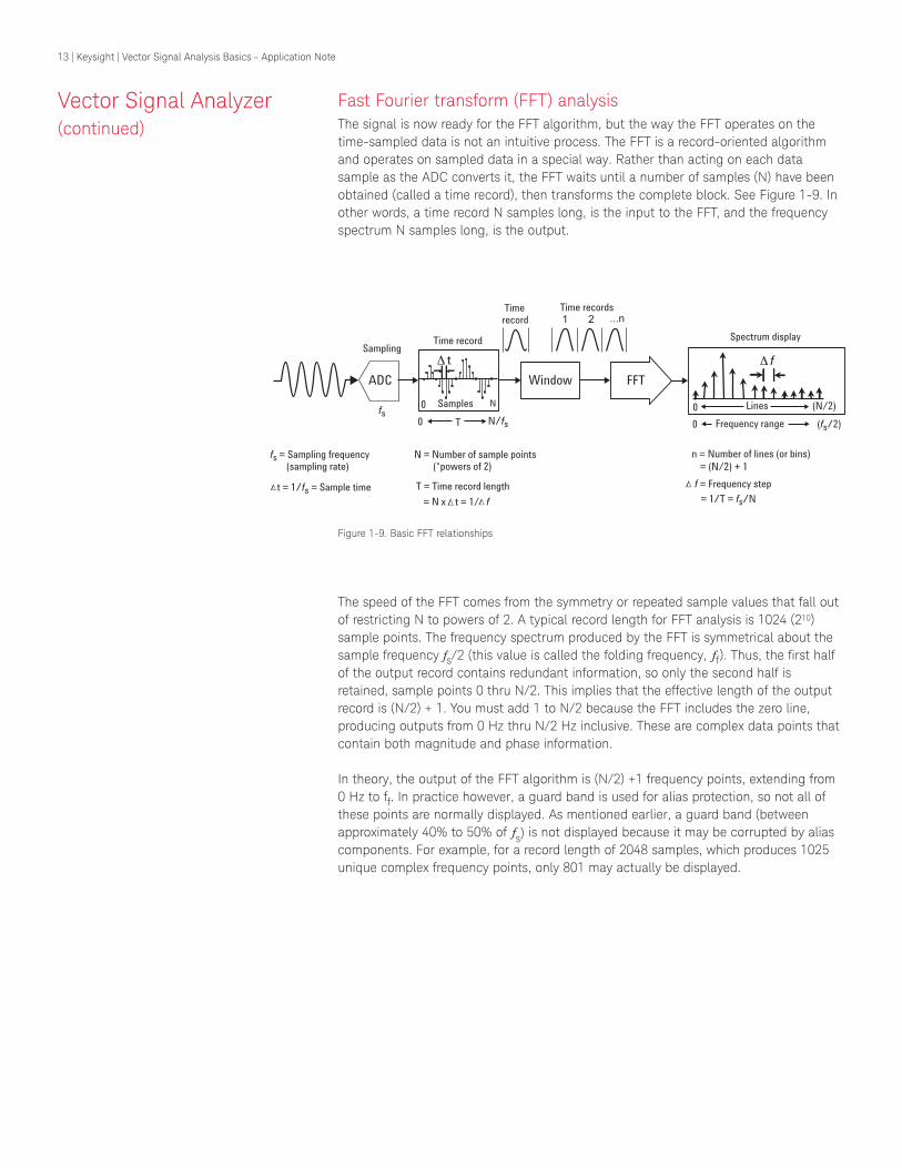
Fast Fourier transform (FFT) analysisThe signal is now ready for the FFT algorithm, but the way the FFT operates on the time-sampled data is not an intuitive process. The FFT is a record-oriented algorithm and operates on sampled data in a special way. Rather than acting on each data sample as the ADC converts it, the FFT waits until a number of samples (N) have been obtained (called a time record), then transforms the complete block. See Figure 1-9. In other words, a time record N samples long, is the input to the FFT, and the frequency spectrum N samples long, is the output.
The speed of the FFT comes from the symmetry or repeated sample values that fall out of restricting N to powers of 2. A typical record length for FFT analysis is 1024 (210) sample points. The frequency spectrum produced by the FFT is symmetrical about the sample frequency fs/2 (this value is called the folding frequency, ff). Thus, the first half of the output record contains redundant information, so only the second half is retained, sample points 0 thru N/2. This implies that the effective length of the output record is (N/2) + 1. You must add 1 to N/2 because the FFT includes the zero line, producing outputs from 0 Hz thru N/2 Hz inclusive. These are complex data points that contain both magnitude and phase information.
In theory, the output of the FFT algorithm is (N/2) +1 frequency points, extending from 0 Hz to ff. In practice however, a guard band is used for alias protection, so not all of these points are normally displayed. As mentioned earlier, a guard band (between approximately 40% to 50% of fs) is not displayed because it may be corrupted by alias components. For example, for a record length of 2048 samples, which produces 1025 unique complex frequency points, only 801 may actually be displayed.
....
.. .....
...
...... .ADC FFT
N = Number of sample points (*powers of 2)
Sampling
fs = Sampling frequency (sampling rate) = (N/2) + 1
Spectrum display
n = Number of lines (or bins)
Δ t
T
= N x t = 1/ f
T = Time record length f = Frequency step
= 1/T = fs/N t = 1/fs = Sample time
Δ f
00 N
Window
Timerecord
Time records1 2 ...n
Time record
Frequency range
Lines (N/2)
0 (fs/2)
Samplesfs
N/fs0
.
Figure 1-9. Basic FFT relationships
Vector Signal Analyzer(continued)
13 | Keysight | Vector Signal Analysis Basics - Application Note
These frequency domain points are called lines, or bins, and are usually numbered from 0 to N/2. These bins are equivalent to the individual filter/detector outputs in a bank-of-filters analyzer. Bin 0 contains the DC level present in the input signal and is referred to as the DC bin. The bins are equally spaced in frequency, with the frequency step (Δf ) being the reciprocal of the measurement time-record length (T). Thus, Δf = 1/T. The length of the time record (T) can be determined from the sample rate ( fs) and the num-ber of sample points (N) in the time record as follows: T = N/ fs. The frequency ( fn) associated with each bin is given by:
fn = n fs/N
where n is the bin number
The frequency of the last bin contains the highest frequency, fs/2. Therefore, the fre-quency range of an FFT is 0 Hz to fs/2. Note that the highest FFT range is not fmax, which is the upper-frequency limit of the analyzer, and may not be the same as the highest bin frequency.
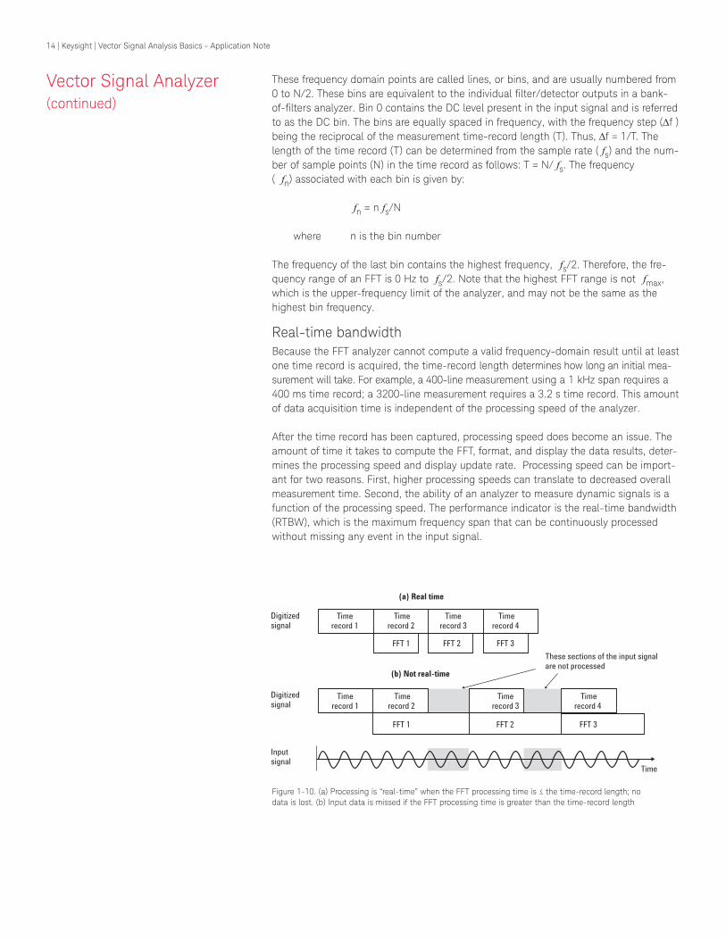
Real-time bandwidthBecause the FFT analyzer cannot compute a valid frequency-domain result until at least one time record is acquired, the time-record length determines how long an initial mea-surement will take. For example, a 400-line measurement using a 1 kHz span requires a 400 ms time record; a 3200-line measurement requires a 3.2 s time record. This amount of data acquisition time is independent of the processing speed of the analyzer.
After the time record has been captured, processing speed does become an issue. The amount of time it takes to compute the FFT, format, and display the data results, deter-mines the processing speed and display update rate. Processing speed can be import-ant for two reasons. First, higher processing speeds can translate to decreased overall measurement time. Second, the ability of an analyzer to measure dynamic signals is a function of the processing speed. The performance indicator is the real-time bandwidth (RTBW), which is the maximum frequency span that can be continuously processed without missing any event in the input signal.
Timerecord 1
Timerecord 2
Timerecord 4
Timerecord 3
FFT 1 FFT 2 FFT 3
FFT 1 FFT 2 FFT 3
Timerecord 1
Timerecord 2
Timerecord 4
Timerecord 3
(b) Not real-time
(a) Real time
These sections of the input signalare not processed
Time
Digitizedsignal
Digitizedsignal
Inputsignal
Figure 1-10. (a) Processing is “real-time” when the FFT processing time is ≤ the time-record length; no data is lost. (b) Input data is missed if the FFT processing time is greater than the time-record length
Vector Signal Analyzer (continued)
14 | Keysight | Vector Signal Analysis Basics - Application Note
In the analyzer, RTBW is the frequency span at which the FFT processing time equals the time-record length. There is no gap between the end of one time record and the start of the next. See Figure 1-10. For any frequency spans less than RTBW, no input data is lost. However, if you increase the span past the real-time bandwidth, the record length becomes shorter than the FFT processing time. When this occurs, the time records are no longer contiguous, and some data will be missed.
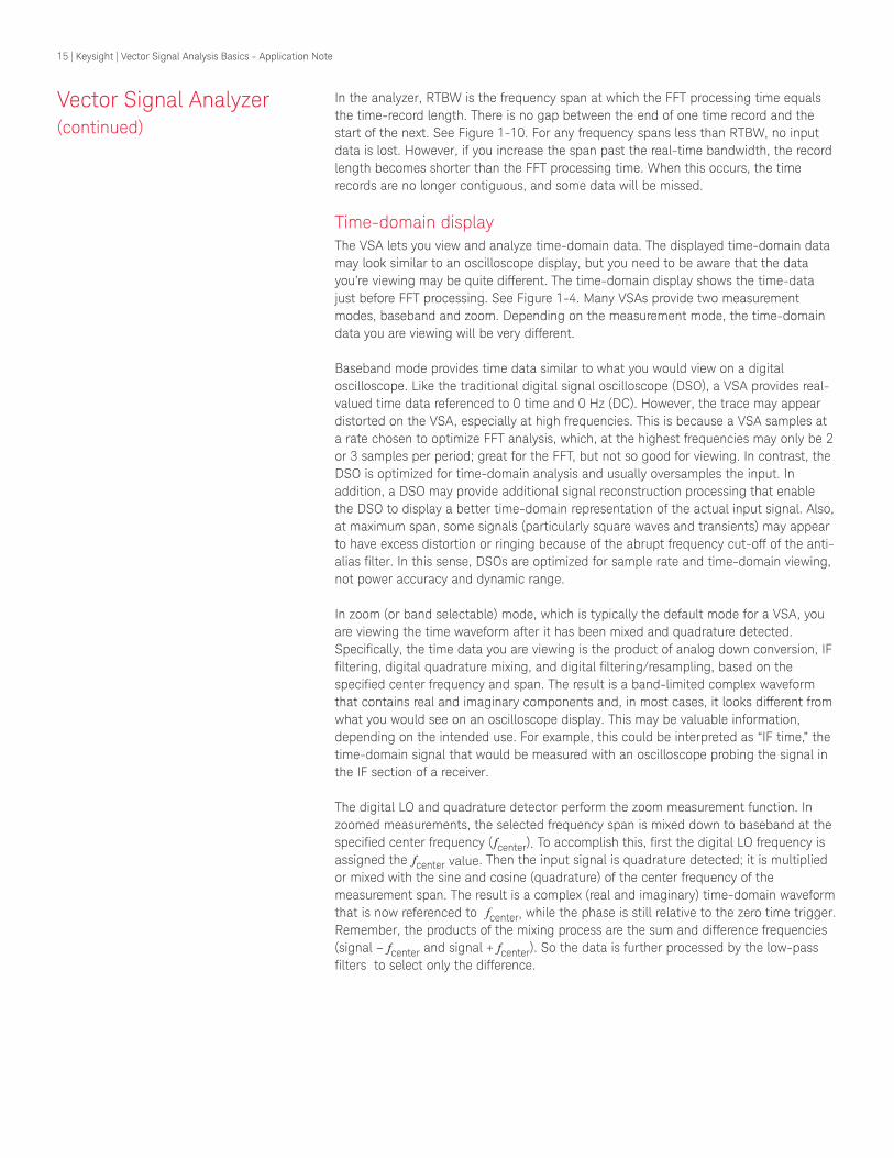
Time-domain displayThe VSA lets you view and analyze time-domain data. The displayed time-domain data may look similar to an oscilloscope display, but you need to be aware that the data you’re viewing may be quite different. The time-domain display shows the time-data just before FFT processing. See Figure 1-4. Many VSAs provide two measurement modes, baseband and zoom. Depending on the measurement mode, the time-domain data you are viewing will be very different.
Baseband mode provides time data similar to what you would view on a digital oscilloscope. Like the traditional digital signal oscilloscope (DSO), a VSA provides real-valued time data referenced to 0 time and 0 Hz (DC). However, the trace may appear distorted on the VSA, especially at high frequencies. This is because a VSA samples at a rate chosen to optimize FFT analysis, which, at the highest frequencies may only be 2 or 3 samples per period; great for the FFT, but not so good for viewing. In contrast, the DSO is optimized for time-domain analysis and usually oversamples the input. In addition, a DSO may provide additional signal reconstruction processing that enable the DSO to display a better time-domain representation of the actual input signal. Also, at maximum span, some signals (particularly square waves and transients) may appear to have excess distortion or ringing because of the abrupt frequency cut-off of the anti-alias filter. In this sense, DSOs are optimized for sample rate and time-domain viewing, not power accuracy and dynamic range.
In zoom (or band selectable) mode, which is typically the default mode for a VSA, you are viewing the time waveform after it has been mixed and quadrature detected. Specifically, the time data you are viewing is the product of analog down conversion, IF filtering, digital quadrature mixing, and digital filtering/resampling, based on the specified center frequency and span. The result is a band-limited complex waveform that contains real and imaginary components and, in most cases, it looks different from what you would see on an oscilloscope display. This may be valuable information, depending on the intended use. For example, this could be interpreted as “IF time,” the time-domain signal that would be measured with an oscilloscope probing the signal in the IF section of a receiver.
The digital LO and quadrature detector perform the zoom measurement function. In zoomed measurements, the selected frequency span is mixed down to baseband at the specified center frequency ( fcenter). To accomplish this, first the digital LO frequency is assigned the fcenter value. Then the input signal is quadrature detected; it is multiplied or mixed with the sine and cosine (quadrature) of the center frequency of the measurement span. The result is a complex (real and imaginary) time-domain waveform that is now referenced to fcenter, while the phase is still relative to the zero time trigger. Remember, the products of the mixing process are the sum and difference frequencies (signal – fcenter and signal + fcenter). So the data is further processed by the low-pass filters to select only the difference.
Vector Signal Analyzer(continued)
15 | Keysight | Vector Signal Analysis Basics - Application Note

frequencies. If the carrier frequency ( fcarrier) is equal to fcenter, the modulation results are the positive and negative frequency sidebands centered about 0 Hz. However, the spectrum displays of the analyzer are annotated to show the correct center frequency and sideband frequency values.
Figure 1-11 shows a 13.5 MHz sinewave measured in both baseband and zoom mode. The span for both measurements is 36 MHz and both start at 0 Hz. The number of frequency points is set to 401. The left-hand time trace shows a sinewave at its true period of approximately 74 ns (1/13.5 MHz). The right-hand time trace shows a sinewave with a period of 222.2 ns (1/4.5 MHz). The 4.5 MHz sinewave is the difference between the 18 MHz VSA center frequency and the 13.5 MHz input signal.
SummaryThis chapter presented a primer on the theory of operation and measurement concepts using a vector signal analyzer (VSA). We went though the system block diagram and described each function as it related to the FFT measurement process. You learned that the implementation used by the VSA is quite different from the conventional analog, swept-tuned analyzer. The VSA is primarily a digital system incorporating an all-digital IF, DSP, and FFT analysis. You learned that the VSA is a test and measurement solution providing time-domain, frequency-domain, modulation-domain and code-domain signal analysis capabilities.
This chapter described the spectrum analysis capabilities of the VSA, implemented thorough FFT analysis. The fundamentals of FFT measurement theory and analysis were presented. The vector analysis measurement concepts and demodulator block, which include digital and analog modulation analysis, are described in Chapter 2.
Figure 1-11. Baseband and zoom time data
Vector Signal Analyzer (continued)
16 | Keysight | Vector Signal Analysis Basics - Application Note
IntroductionChapter 1 was a primer on vector signal analyzers (VSA) and discussed VSA measurement concepts and theory of operation. It also described the frequency-domain, spectrum analysis measurement capability of the VSA, implemented through fast Fourier transform (FFT) analysis. This chapter describes the vector-modulation analysis and digital-modulation analysis measurement capability of the VSA. Some swept-tuned spectrum analyzers can also provide digital-modulation analysis by incorporating additional digital radio personality software. However, VSAs typically provide more measurement flexibility in terms of modulation formats and demodulator configuration, and provide a larger set of data results and display traces. The basic digital-modulation analysis concepts described in this chapter can also apply to swept-tuned analyzers that have the additional digital-modulation analysis software.
The real power of the VSA is its ability to measure and analyze vector-modulated and digitally modulated signals. Vector-modulation analysis means the analyzer can measure complex signals, signals that have a real and imaginary component. Since digital communications systems use complex signals (I-Q waveforms), vector-modulation analysis is required to measure digitally-modulated signals. But vector-modulation analysis is not enough to measure today’s complicated digitally-modulated signals. You also need digital-modulation analysis. Digital-modulation analysis is needed to demodulate the RF modulated carrier signal into its complex components (the I-Q waveforms) so you can apply vector-modulation analysis. Vector modulation analysis provides the numerical and visual tools to help quickly identify and quantify impairments to the I-Q waveforms. Digital-modulation analysis is also needed to detect and recover the digital data bits.
Digital demodulation also provides modulation quality measurements. The technique used in Keysight VSAs (described later in this chapter) can expose very subtle signal variations, which translates into signal quality information not available from traditional modulation quality measurement methods. Various display formats and capabilities are used to view the baseband signal characteristics and analyze modulation quality. The VSA offers traditional display formats such as I-Q vector, constellation, eye, and trellis diagrams. The symbol/error summary table shows the actual recovered bits and valuable error data, such as error vector magnitude (EVM), magnitude error, phase error, frequency error, rho, and I-Q offset error. Other display formats, such as magnitude/phase error versus time, magnitude/phase error versus frequency, or equalization allow you to make frequency response and group delay measurements or see code-domain results. This is only a representative list of available display formats and capabilities. Those available in a VSA are dependent upon analyzer capability and the type of digital-modulation format being measured.
Chapter 2 Vector Modulation Analysis
17 | Keysight | Vector Signal Analysis Basics - Application Note

The VSA, with digital modulation provides measurement support for multiple digital communication standards, such as GSM, EDGE, W-CDMA, and cdma2000. Measurements are possible on continuous or burst carriers (such as TDMA), and you can make measurements at baseband, IF, and RF locations throughout a digital communications system block diagram. There is no need for external filtering, coherent carrier signals, or symbol clock timing signals. The general-purpose design of the digital demodulator in the VSA also allows you to measure non-standard formats, allowing you to change user-definable digital parameters for customized test and analysis purposes.
Another important measurement tool that vector-modulation analysis provides is analog-modulation analysis. For example, the Keysight 89600 VSA provides analog-modulation analysis and produces AM, FM, and PM demodulation results, similar to what a modulation analyzer would produce, allowing you to view amplitude, frequency, and phase profiles versus time. These additional analog-demodulation capabilities can be used to troubleshoot particular problems in a digital communications transmitter. For example, phase demodulation is often used to troubleshoot instability at a particular LO frequency.
The remainder of this chapter contains additional concepts to help you better understand vector-modulation analysis, digital-modulation analysis, and analog-modulation analysis.
Vector modulation and digital modulation overviewLet’s begin our discussion by reviewing vector modulation and digital modulation. Digital modulation is a term used in radio, satellite, and terrestrial communications to refer to modulation in which digital states are represented by the relative phase and/or amplitude of the carrier. Although we talk about digital modulation, you should remember that the modulation is not digital, but truly analog. Modulation is the amplitude, frequency, or phase modification of the carrier in direct proportion to the amplitude of the modulating (baseband) signal. See Figure 2-1. In digital modulation, it is the baseband modulating signal, not the modulation process, that is in digital form.
Frequency
Amplitude
Amplitude & phase
Phaset
t
t
t
Digital basebandmodulating signal
Digital data1 0 1 0
Figure 2-1. In digital modulation, the information is contained in the relative phase, frequency, or ampli-tude of the carrier
Vector Modulation Analysis (continued)
18 | Keysight | Vector Signal Analysis Basics - Application Note

Depending on the particular application, digital modulation may modify amplitude, frequency, and phase simultaneously and separately. This type of modulation could be accomplished using conventional analog modulation schemes like amplitude modulation (AM), frequency modulation (FM), or phase modulation (PM). However, in practical systems, vector modulation(also called complex or I-Q modulation) is used instead. Vector modulation is a very powerful scheme because it can be used to generate any arbitrary carrier phase and magnitude. In this scheme, the baseband digital information is separated into two independent components: the I (In-phase) and Q (Quadrature) components. These I and Q components are then combined to form the baseband modulating signal. The most important characteristic of I and Q components is that they are independent components (orthogonal). You’ll learn more about I and Q components and why digital systems use them in the following discussion.
An easy way to understand and view digital modulation is with the I-Q or vector diagram shown in Figure 2-2. In most digital communication systems, the frequency of the carrier is fixed so only phase and magnitude need to be considered. The unmodulated carrier is the phase and frequency reference, and the modulated signal is interpreted relative to the carrier. The phase and magnitude can be represented in polar or vector coordinates as a discrete point in the I-Q plane. See Figure 2-2. I represents the in-phase (phase reference) component and Q represents the quadrature (90° out of phase) component. You can also represent this discrete point by vector addition of a specific magnitude of in-phase carrier with a specific magnitude of quadrature carrier. This is the principle of I-Q modulation.
I (volts)
Q (volts) (Q uadrature orimaginary part)
(In-phase or real part)
Q - value
I - value
0 deg (carrier phase reference)
(I ,Q )1 1
Magnitude
θ Phase
A discrete point on the I-Q diagramrepresents a digital state or symbol location
1
1–1
–1
Figure 2-2. Digital modulation I-Q diagram
Vector Modulation Analysis (continued)
19 | Keysight | Vector Signal Analysis Basics - Application Note
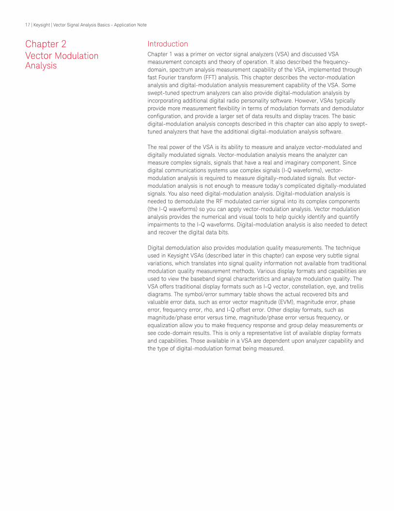
By forcing the carrier to one of several predetermined positions in the I-Q plane, you can then transmit encoded information. Each position or state (or transitions between the states in some systems) represents a certain bit pattern that can be decoded at the receiver. The mapping of the states or symbols at each symbol timing instant (when the receiver interprets the signal) on the I-Q plane is referred to as a constellation diagram. See Figure 2-3. A symbol represents a grouping of the digital data bits; they are symbolic of the digital words they represent. The number of bits contained in each symbol, or bits-per-symbol (bpsym), is determined by the modulation format. For example, binary phase shift keying (BPSK) uses 1 bpsym, quadrature phase shift keying (QPSK) uses 2 bpsym, and 8-state phase shift keying (8PSK) uses 3 bpsym. Theoretically, each state location on the constellation diagram should show as a single point, but a practical system suffers from various impairments and noise that cause a spreading of the states (a dispersal of dots around each state). Figure 2-3 shows the constellation or state diagram for a 16 QAM (16-state quadrature amplitude modulation) format; note that there are 16 possible state locations. This format takes four bits of serial data and encodes them as single amplitude/phase states, or symbols. In order to generate this modulation format, the I and Q carriers each need to take four different levels of amplitude, depending on the code being transmitted.
In digital modulation, the signal moves among a limited number of symbols or states. The rate at which the carrier moves between points in the constellation is called the symbol rate. The more constellation states that are used, the lower the required symbol rate for a given bit rate. The symbol rate is important because it tells you the bandwidth required to transmit the signal. The lower the symbol rate, the less bandwidth required for transmission. For example, the 16QAM format, mentioned earlier, uses 4 bits per symbol. If the radio transmission rate is 16 Mbps, then the symbol rate = 16 (Mbps) divided by 4 bits, or 4 MHz. This provides a symbol rate that is one-fourth the bit rate and a more spectrally efficient transmission bandwidth (4 MHz versus 16 MHz). For more detailed information about digital modulation, see the References section at the end of this application note.
I
Q
Constellation or state diagram
16 QAM
0000000100100011
0100010101100111
1000100110101011
1100110111101111
–1
1
-1
1
(volts)
0
I
Q
1V
–1V
0
1V
–1V
0
01 00
serial bit stream
t
t
Symbol mapping to IQ voltages
t1 2 3 4
symbol timing instants
(volts)
symbols
state: 0100symbol: 1I = 1 VQ = 0.5 V
00 01 11 01 00 10
Figure 2-3. Each position, or state, in the constellation diagram represents a specific bit pattern (symbol) and symbol time
Vector Modulation Analysis (continued)
20 | Keysight | Vector Signal Analysis Basics - Application Note
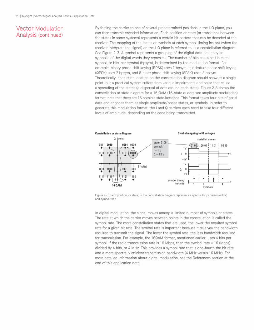
I-Q modulator
The device used in digital communications to generate vector modulation is the I-Q modulator. The I-Q modulator puts the encoded digital I and Q baseband information onto the carrier. See Figure 2-4. The I-Q modulator generates signals in terms of I and Q components; fundamentally it is a hardware (or software) implementation of a rectangular to polar coordinate conversion.
The I-Q modulator receives the I and Q baseband signals as inputs and mixes them with the same local oscillator (LO). Thus, I and Q are both upconverted to the RF carrier frequency. The I information amplitude modulates the carrier producing the in-phase component. The Q information amplitude modulates a 90-degree (orthogonal) phase shifted version of the carrier producing the quadrature component. These two orthogonal modulated carrier signals are summed together producing the composite I-Q modulated carrier signal. The main advantage of I-Q modulation is the symmetric ease of combining independent signal components into a single, composite signal, and later splitting the composite signal into its independent component parts.
Signals that are separated by 90 degrees are known as being orthogonal to each other, or in quadrature. The quadrature relationship between I and Q signals means that these two signals are truly independent. They are two independent components of the same signal. While changes of the Q input certainly alter the composite output signal, they do not change the I component at all. Similarly, changes of the I input have no effect on the Q signal.
90 deg.phase shift
(Q uadrature component)
(In-phase component)
Compositeoutput signal(I-Q modulated carrier)
Rectangularcoordinates
Polarcoordinates
Summingcircuits
I baseband
Local oscillator(carrier frequency)
Q baseband
Σ
Figure 2-4. I-Q modulator
Vector Modulation Analysis (continued)
21 | Keysight | Vector Signal Analysis Basics - Application Note
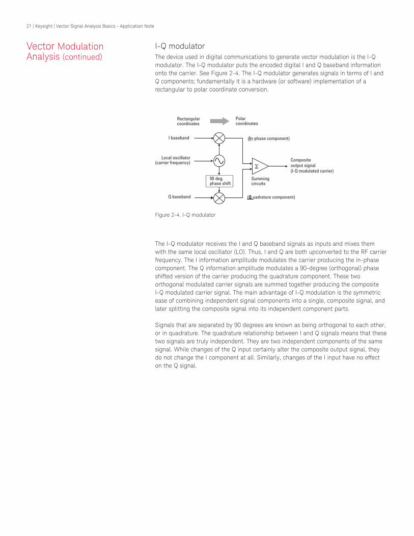
I-Q demodulatorAs you can see in Figure 2-5, the I-Q demodulator is a mirror image of the I-Q modulator shown in Figure 2-4. The I-Q demodulator recovers the original I and Q baseband signals from a composite I-Q modulated input signal.
The first step in the demodulation process is to phase-lock the receiver LO to the transmitter carrier frequency. It is necessary that the receiver LO be phase-locked to the transmitter carrier (or mixer LO) to correctly recover the I and Q baseband components. Then, the I-Q modulated carrier is mixed with both an unshifted LO, and a 90 degree phase-shifted version of the LO, producing the original I and Q baseband signals or components.
The I-Q demodulation process is fundamentally a polar to rectangular conversion. Normally, information cannot be plotted in a polar format and reinterpreted as rectangular values without doing a polar-to-rectangular conversion. See Figure 2-2.1 However, this conversion is exactly what is done by the in-phase and quadrature mixing processes performed by the I-Q demodulator.
Why use I and Q?Digital modulation uses I and Q components because it provides a simple, efficient, and robust modulation method for generating, transmitting, and recovering digital data. Modulated signals in the I-Q domain provide many advantages:
1. The I-Q implementation provides a method to create complex signals (both phase and amplitude change). Instead of using phase modulation, which is nonlinear and difficult to do well, the I-Q modulator simply modulates the amplitude of the carrier and its quadrature in a linear manner. Mixers with wide modulation bandwidths and good linearity are readily available. To produce a complex modulated signal, you only need to generate the baseband I and Q components of the signal. One key advantage of I-Q modulators is that the same modulator can be used to generate a variety of modulations from digital formats to RF pulses, or even radar chirps, for example.
2. Demodulating the signal is also straightforward. Using an I-Q demodulator, it is simple, at least in principle, to recover the baseband signals.
3. Looking at a signal in the I-Q plane often gives good insights about the signal. Effects like cross talk, data skew, compression, and AM-to-PM distortion, which are hard to visualize otherwise, are easy to see.
Compositeinput signal
(I-Q modulated carrier)
Local oscillator(phase locked to thecarrier frequency)
90 deg.phase shift
I baseband(In-phase component)
Q baseband(Q uadrature component)
Polarcoordinates
Rectangularcoordinates
Powersplitter
Figure 2-5. I-Q demodulator (or quadrature detector)
Vector Modulation Analysis (continued)
22 | Keysight | Vector Signal Analysis Basics - Application Note
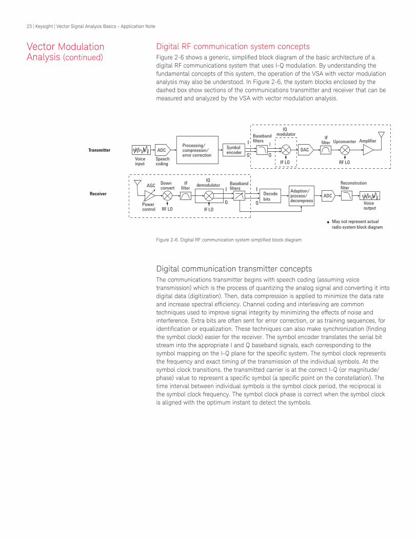
Digital RF communication system conceptsFigure 2-6 shows a generic, simplified block diagram of the basic architecture of a digital RF communications system that uses I-Q modulation. By understanding the fundamental concepts of this system, the operation of the VSA with vector modulation analysis may also be understood. In Figure 2-6, the system blocks enclosed by the dashed box show sections of the communications transmitter and receiver that can be measured and analyzed by the VSA with vector modulation analysis.
Digital communication transmitter conceptsThe communications transmitter begins with speech coding (assuming voice transmission) which is the process of quantizing the analog signal and converting it into digital data (digitization). Then, data compression is applied to minimize the data rate and increase spectral efficiency. Channel coding and interleaving are common techniques used to improve signal integrity by minimizing the effects of noise and interference. Extra bits are often sent for error correction, or as training sequences, for identification or equalization. These techniques can also make synchronization (finding the symbol clock) easier for the receiver. The symbol encoder translates the serial bit stream into the appropriate I and Q baseband signals, each corresponding to the symbol mapping on the I-Q plane for the specific system. The symbol clock represents the frequency and exact timing of the transmission of the individual symbols. At the symbol clock transitions, the transmitted carrier is at the correct I-Q (or magnitude/phase) value to represent a specific symbol (a specific point on the constellation). The time interval between individual symbols is the symbol clock period, the reciprocal is the symbol clock frequency. The symbol clock phase is correct when the symbol clock is aligned with the optimum instant to detect the symbols.
Transmitter
Receiver
AGCI I
Decodebits
Adaption/process/decompress
Processing/compression/error correction
Symbolencoder DAC
I I
Q
Q
IF LO RF LO
Q
Voiceinput
Voiceoutput
Q
IFfilter
Basebandfilters
Speechcoding
Basebandfilters
IQmodulator
Upconverter Amplifier
Powercontrol
ADC
RF LO
Downconvert
IFfilter
ADC
IF LO
IQdemodulator
May not represent actualradio system block diagram
Reconstrutionfilter
Figure 2-6. Digital RF communication system simplified block diagram
Vector Modulation Analysis (continued)
23 | Keysight | Vector Signal Analysis Basics - Application Note
Once the I and Q baseband signals have been generated, they are filtered (band limit-ed) to improve spectral efficiency. An unfiltered output of the digital radio modulator occupies a very wide bandwidth (theoretically, infinite). This is because the modulator is being driven by baseband I-Q square waveswith fast transitions; fast transitions in the time domain equate to wide frequency spectra in the frequency domain. This is an unacceptable condition because it decreases the available spectrum to other users and causes signal interference to nearby users, called adjacent-channel-power interference. Baseband filtering solves the problem by limiting the spectrum and restricting interfer-ence with other channels. In effect, the filtering slows the fast transitions between states, thereby limiting the frequency spectrum. Filtering is not without tradeoffs, how-ever; filtering also causes degradation to the signal and data transmission.
The signal degradation is due to reduction of spectral content and the overshoot and finite ringing caused by the filters time (impulse) response. By reducing the spectral content, information is lost and it may make reconstructing the signal difficult, or even impossible, at the receiver. The ringing response of the filter may last so long so that it affects symbols that follow, causing intersymbol interference (ISI). ISI is defined as the extraneous energy from prior and subsequent symbols that interferes with the current symbol such that the receiver misinterprets the symbol. Thus, selecting the best filter becomes a design compromise between spectral efficiency and minimizing ISI. There is a common, special class of filters used in digital communication design called Nyquist filters. Nyquist filters are an optimal filter choice because they maximize data rates, minimize ISI, and limit channel bandwidth requirements. You will learn more about fil-ters later in this chapter. To improve the overall performance of the system, filtering is often shared, or split, between the transmitter and the receiver. In that case, the filters must be as closely matched as possible and correctly implemented, in both transmitter and receiver, to minimize ISI. Figure 2-6 only shows one baseband filter, but in reality, there are two; one each for the I and Q channel.
The filtered I and Q baseband signals are inputs to the I-Q modulator. The LO in the modulator may operate at an intermediate frequency (IF) or directly at the final radio frequency (RF). The output of the modulator is the composite of the two orthogonal I and Q signals at the IF (or RF). After modulation, the signal is upconverted to RF, if needed. Any undesirable frequencies are filtered out and the signal is applied to the output amplifier and transmitted.
Vector Modulation Analysis (continued)
24 | Keysight | Vector Signal Analysis Basics - Application Note
Digital communications receiver concepts
The receiver is essentially an inverse implementation of the transmitter, but it is more complex to design. The receiver first downconverts the incoming RF signal to IF, then demodulates it. The ability to demodulate the signal and recover the original data is often difficult. The transmitted signal is often corrupted by such factors as atmospheric noise, competing signal interference, multipath, or fading.
The demodulation process involves these general stages: carrier frequency recovery (carrier lock), symbol clock recovery (symbol lock), signal decomposition to I and Q components (I-Q demodulation), I and Q symbol detection, bit decoding and de-interleaving (decode bits), decompressing (expansion to original bit stream), and finally, digital to analog conversion (if required).
The main difference between the transmitter and receiver is the need for carrier and symbol clock recovery. Both the symbol clock frequency and phase (or timing) must be correct in the receiver to demodulate the bits successfully and recover the transmitted information. For example, the symbol clock could be set to the correct frequency, but at the wrong phase. That is, if the symbol clock is aligned to the transitions between symbols, rather than the symbols themselves, demodulation will be unsuccessful.
A difficult task in receiver design is to create carrier and symbol clock recovery algorithms. Some clock recovery techniques include measuring the modulation amplitude variations, or in systems with pulsed carriers, the power turn-on event can be used. This task can also be made easier when channel coding in the transmitter provides training sequences or synchronization bits.
Vector Modulation Analysis (continued)
25 | Keysight | Vector Signal Analysis Basics - Application Note

VSA digital modulation analysis concepts and theory of operationThe VSA can be viewed as a measuring receiver. It is really an I-Q receiver employing techniques similar to most digital radio receivers for decoding digital modulations. However, the difference is that the VSA is designed for high accuracy parametric measurement and display of modulation characteristics. Moreover, the VSA is a measurement tool that can measure and analyze almost every aspect of a digital communications transmitter and receiver system.
Figure 2-7 shows a Keysight 89600 VSA simplified system block diagram. You may notice that many of the VSA system blocks are analogous to the digital communication receiver shown in Figure 2-6. The RF input signal is downconverted, through several stages of superheterodyne mixing, to an IF that can be accurately digitized by the ADC. This digitized IF is then vector (quadrature) detected and digitally filtered; downconverted one last time to an I and Q baseband form (I-Q time data) and stored in RAM. From here, DSP algorithms demodulate the signal; recover the carrier and symbol clock and apply reconstructive filtering and decoding (recover the original bits). With this DSP software implementation, almost any modulation format can be demodulated.
The VSA implementation is different from a radio receiver. The VSA deals with the sampled signals on a block basis; the radio receiver processes data serially, in real time. When you supply the VSA with radio receiver parameters, the VSA synthesizes the receiver via processing in the DSP. It provides all the functions of a receiver, down to making analog waveforms. Because the signal has been virtually digitized, it can be post-processed and viewed in any of the time, frequency, or modulation domains.
ADC
IQ b
aseb
and
time
data
Anti-alias filter
Quadrature detector,digital filter
FFT
LO
RFinput
Demodulator
• Digital demod
• Analog demod
Samplememory
Dis
play
Vector modulationanalysis
Spectrum analysis
Note: Actual VSA implementation may be different.
Digital LO
Time-domain
Freq-domain
Modulation-domain
Code-domain
Analog IF Re-sampled,
corrected,time data
I
Q
Digital IF
90 ϒ
Figure 2-7. The VSA demodulator performs vector signal analysis, including digital and analog modulation analysis
Vector Modulation Analysis (continued)
26 | Keysight | Vector Signal Analysis Basics - Application Note
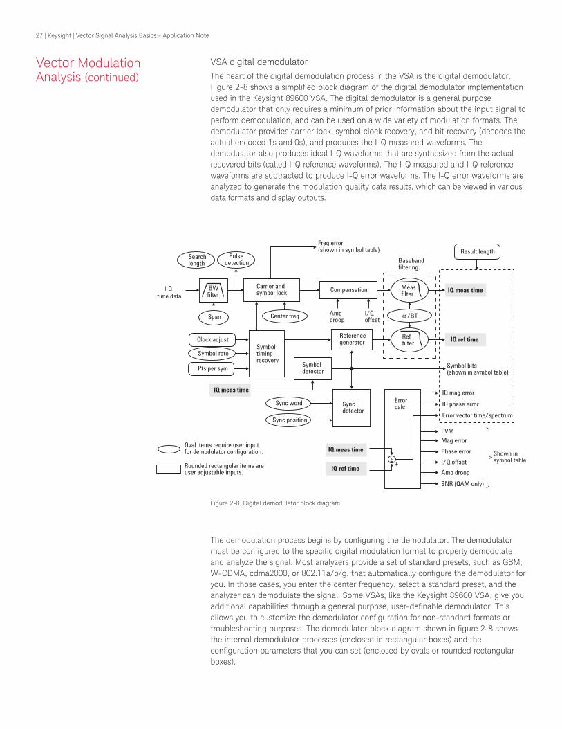
VSA digital demodulator
The heart of the digital demodulation process in the VSA is the digital demodulator. Figure 2-8 shows a simplified block diagram of the digital demodulator implementation used in the Keysight 89600 VSA. The digital demodulator is a general purpose demodulator that only requires a minimum of prior information about the input signal to perform demodulation, and can be used on a wide variety of modulation formats. The demodulator provides carrier lock, symbol clock recovery, and bit recovery (decodes the actual encoded 1s and 0s), and produces the I-Q measured waveforms. The demodulator also produces ideal I-Q waveforms that are synthesized from the actual recovered bits (called I-Q reference waveforms). The I-Q measured and I-Q reference waveforms are subtracted to produce I-Q error waveforms. The I-Q error waveforms are analyzed to generate the modulation quality data results, which can be viewed in various data formats and display outputs.
The demodulation process begins by configuring the demodulator. The demodulator must be configured to the specific digital modulation format to properly demodulate and analyze the signal. Most analyzers provide a set of standard presets, such as GSM, W-CDMA, cdma2000, or 802.11a/b/g, that automatically configure the demodulator for you. In those cases, you enter the center frequency, select a standard preset, and the analyzer can demodulate the signal. Some VSAs, like the Keysight 89600 VSA, give you additional capabilities through a general purpose, user-definable demodulator. This allows you to customize the demodulator configuration for non-standard formats or troubleshooting purposes. The demodulator block diagram shown in figure 2-8 shows the internal demodulator processes (enclosed in rectangular boxes) and the configuration parameters that you can set (enclosed by ovals or rounded rectangular boxes).
Error vector time/spectrum
IQ phase error
IQ mag error
EVM
Mag error
Phase error
I/Q offset
Amp droop
SNR (QAM only)
Shown insymbol table
Symbol bits(shown in symbol table)
IQ ref time
IQ meas timeMeasfilter
Freq error(shown in symbol table)
Carrier andsymbol lock
Ampdroop
I/Qoffset
Symboltimingrecovery
/BTα
Result length
Compensation
Center freq
Clock adjust
Symbol rate
Pts per sym
Sync word
Sync position
Reffilter
Errorcalc
I-Qtime data
BWfilter
Span
Pulsedetection
Searchlength
Oval items require user inputfor demodulator configuration.
Rounded rectangular items areuser adjustable inputs.
–
+
IQ meas time
IQ meas time
IQ ref time
Basebandfiltering
Symboldetector
Referencegenerator
Syncdetector
Σ
Figure 2-8. Digital demodulator block diagram
Vector Modulation Analysis (continued)
27 | Keysight | Vector Signal Analysis Basics - Application Note

The items enclosed by an oval identify configuration parameters that are required to define the demodulator for a measurement. The rounded rectangular boxes identify user-adjustable input parameters. At a minimum, the demodulator requires the modulation format (QPSK, FSK, and so forth), the symbol rate, the baseband filter type, and filter alpha/BT. This set of parameters is generally sufficient for the demodulator to lock to the signal and recover the symbols.
The demodulator uses the configuration inputs and, through DSP, operates on the I-Q time data received in block format from the sample memory of the analyzer. The VSA can also receive I-Q time data from external hardware (such as a Keysight PSA or ESA Series spectrum analyzer or Infiniium 54800 Series oscilloscope) or from a recorded file. The demodulator uses the supplied center frequency and symbol rate to lock to the carrier and recover the symbol clock from the modulated carrier. Note that the demodulator reference clock does not need to be locked with the source clock. The demodulator automatically provides carrier and symbol lock, you do not need to supply an external source clock input. The signal then goes through a compensation process that applies gain and phase correction. The compensation data (such as amplitude droop and I-Q offset error data) is stored and can be viewed in the error summary table. Digital baseband filtering is then applied to recover the baseband I-Q waveforms (I-Q Meas Time data). The recovered I-Q waveforms are applied to a symbol detector that attempts to determine what symbols were transmitted, based upon the specified modulation format. From this block of symbols, the serial data bits (1s and 0s) are decoded and recovered.
The reference generator uses the detected symbols in conjunction with the modulation format, the symbol rate, and the specified filtering, to synthesize an ideal set of I-Q reference baseband waveforms (I-Q Ref Time data). Finally, the measured I/Q waveforms and reference I-Q waveforms are compared to produce a host of error characteristics (deviation from perfect) such as phase error, magnitude error, and error vector magnitude (EVM).
I-Q measurement and I-Q reference signalThe quality of an I-Q modulated signal can be analyzed by comparing the measured signal to an ideal reference signal. See Figure 2-9. The demodulator produces two waveforms: an I-Q measured waveform and an I-Q reference waveform. The I-Q measured waveform is the demodulated baseband I-Q data for the measured input signal, also called IQ Meas Time. The I-Q reference waveform is the baseband I-Q data that would result after demodulating the input signal if the input signal were ideal (contained no errors), also called IQ Ref Time.
The I-Q reference waveform is mathematically derived from the I-Q measured waveform recovered data bits, providing that the original data sequence can be recovered. The I-Q reference waveform generation begins by recovering the actual symbol bits from the demodulated I-Q measured waveform, and then reconstructing a sequence of ideal I and Q states. These states are then treated as ideal impulses and are baseband filtered according to the reference channel filtering, producing an ideal I-Q reference waveform.
The quality of the input signal can then be analyzed by comparing the I-Q measured waveform to the I-Q reference waveform. Subtracting the reference waveform from the measured waveform provides the error vector waveform, or I-Q error waveform. This technique can expose very subtle signal variations, which translates into signal quality information not available from traditional modulation quality measurement methods.
Vector Modulation Analysis (continued)
28 | Keysight | Vector Signal Analysis Basics - Application Note
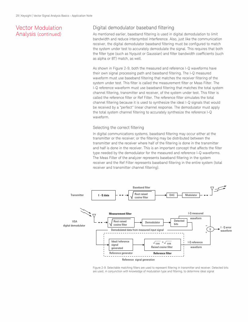
Digital demodulator baseband filtering
As mentioned earlier, baseband filtering is used in digital demodulation to limit bandwidth and reduce intersymbol interference. Also, just like the communication receiver, the digital demodulator baseband filtering must be configured to match the system under test to accurately demodulate the signal. This requires that both the filter type (such as Nyquist or Gaussian) and filter bandwidth coefficients (such as alpha or BT) match, as well.
As shown in Figure 2-9, both the measured and reference I-Q waveforms have their own signal processing path and baseband filtering. The I-Q measured waveform must use baseband filtering that matches the receiver filtering of the system under test. This filter is called the measurement filter or Meas Filter. The I-Q reference waveform must use baseband filtering that matches the total system channel filtering, transmitter and receiver, of the system under test. This filter is called the reference filter or Ref Filter. The reference filter simulates the total channel filtering because it is used to synthesize the ideal I-Q signals that would be received by a “perfect” linear channel response. The demodulator must apply the total system channel filtering to accurately synthesize the reference I-Q waveform.
Selecting the correct filtering
In digital communications systems, baseband filtering may occur either at the transmitter or the receiver; or the filtering may be distributed between the transmitter and the receiver where half of the filtering is done in the transmitter and half is done in the receiver. This is an important concept that affects the filter type needed by the demodulator for the measured and reference I-Q waveforms. The Meas Filter of the analyzer represents baseband filtering in the system receiver and the Ref Filter represents baseband filtering in the entire system (total receiver and transmitter channel filtering).
Demodulator
Reference filter
Transmitter I - Q data
Raised cosine filter
DAC
I - Q errorwaveform
VSA
digital demodulator
Ideal/referencesignalgenerated
I-Q measured
waveformRoot raisedcosine filter
Measurement filter
Reference signal generation
Modulator
I-Q reference
waveform
+S
coscos ×
Detectedbits
Baseband filter
Root raisedcosine filter
Demodulated data from measured input signal
Reference generator
Figure 2-9. Selectable matching filters are used to represent filtering in transmitter and receiver. Detected bits are used, in conjunction with knowledge of modulation type and filtering, to determine ideal signal
Vector Modulation Analysis (continued)
29 | Keysight | Vector Signal Analysis Basics - Application Note
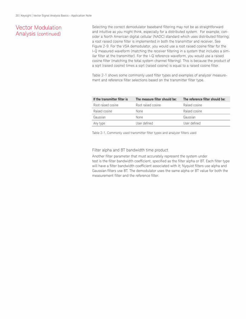
Selecting the correct demodulator baseband filtering may not be as straightforward and intuitive as you might think, especially for a distributed system. For example, con-sider a North American digital cellular (NADC) standard which uses distributed filtering; a root raised cosine filter is implemented in both the transmitter and receiver. See Figure 2-9. For the VSA demodulator, you would use a root raised cosine filter for the I-Q measured waveform (matching the receiver filtering in a system that includes a sim-ilar filter at the transmitter). For the I-Q reference waveform, you would use a raised cosine filter (matching the total system channel filtering). This is because the product of a sqrt (raised cosine) times a sqrt (raised cosine) is equal to a raised cosine filter.
Table 2-1 shows some commonly used filter types and examples of analyzer measure-ment and reference filter selections based on the transmitter filter type.
Filter alpha and BT bandwidth time product Another filter parameter that must accurately represent the system under test is the filter bandwidth coefficient, specified as the filter alpha or BT. Each filter type will have a filter bandwidth coefficient associated with it; Nyquist filters use alpha and Gaussian filters use BT. The demodulator uses the same alpha or BT value for both the measurement filter and the reference filter.
Vector Modulation Analysis (continued)
If the transmitter filter is The measure filter should be: The reference filter should be:
Root raised cosine Root raised cosine Raised cosine
Raised cosine None Raised cosine
Gaussian None Gaussian
Any type User defined User defined
Table 2-1. Commonly used transmitter filter types and analyzer filters used
30 | Keysight | Vector Signal Analysis Basics - Application Note
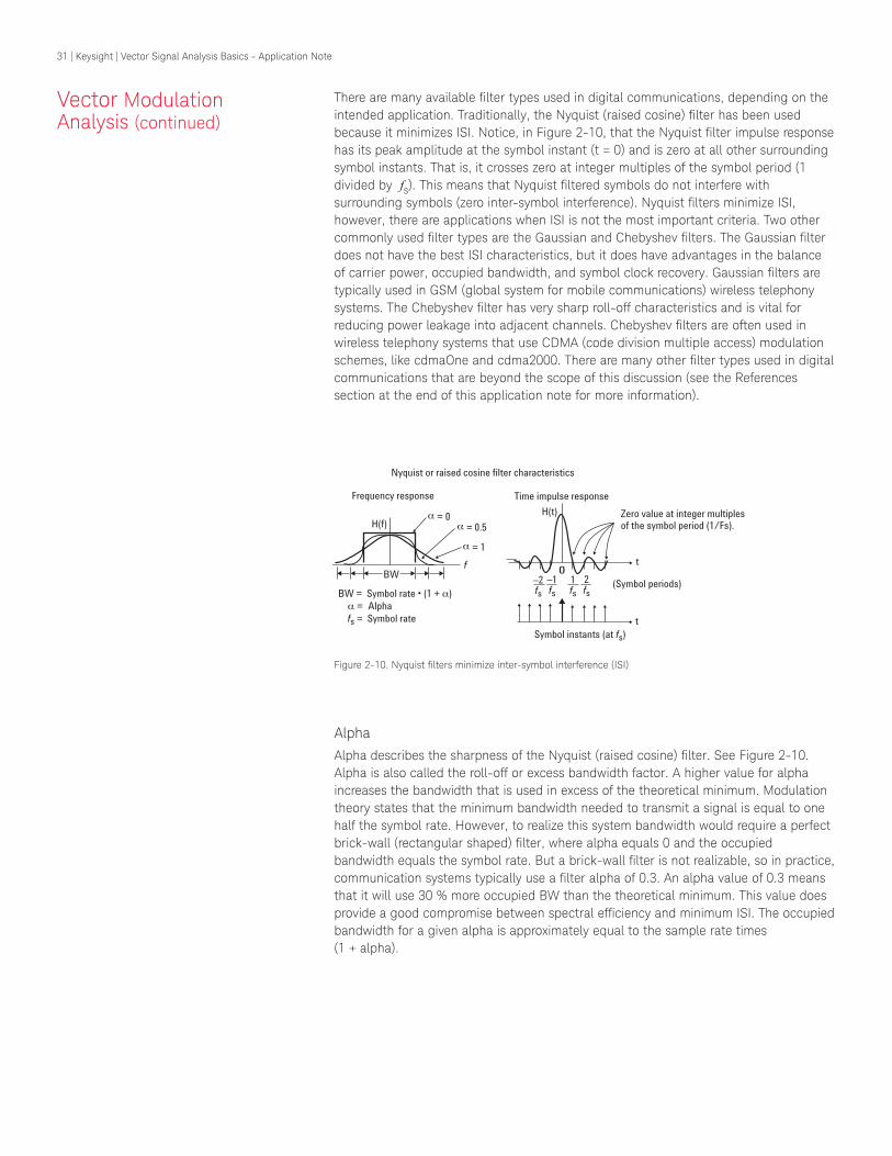
There are many available filter types used in digital communications, depending on the intended application. Traditionally, the Nyquist (raised cosine) filter has been used because it minimizes ISI. Notice, in Figure 2-10, that the Nyquist filter impulse response has its peak amplitude at the symbol instant (t = 0) and is zero at all other surrounding symbol instants. That is, it crosses zero at integer multiples of the symbol period (1 divided by fs). This means that Nyquist filtered symbols do not interfere with surrounding symbols (zero inter-symbol interference). Nyquist filters minimize ISI, however, there are applications when ISI is not the most important criteria. Two other commonly used filter types are the Gaussian and Chebyshev filters. The Gaussian filter does not have the best ISI characteristics, but it does have advantages in the balance of carrier power, occupied bandwidth, and symbol clock recovery. Gaussian filters are typically used in GSM (global system for mobile communications) wireless telephony systems. The Chebyshev filter has very sharp roll-off characteristics and is vital for reducing power leakage into adjacent channels. Chebyshev filters are often used in wireless telephony systems that use CDMA (code division multiple access) modulation schemes, like cdmaOne and cdma2000. There are many other filter types used in digital communications that are beyond the scope of this discussion (see the References section at the end of this application note for more information).
Alpha
Alpha describes the sharpness of the Nyquist (raised cosine) filter. See Figure 2-10. Alpha is also called the roll-off or excess bandwidth factor. A higher value for alpha increases the bandwidth that is used in excess of the theoretical minimum. Modulation theory states that the minimum bandwidth needed to transmit a signal is equal to one half the symbol rate. However, to realize this system bandwidth would require a perfect brick-wall (rectangular shaped) filter, where alpha equals 0 and the occupied bandwidth equals the symbol rate. But a brick-wall filter is not realizable, so in practice, communication systems typically use a filter alpha of 0.3. An alpha value of 0.3 means that it will use 30 % more occupied BW than the theoretical minimum. This value does provide a good compromise between spectral efficiency and minimum ISI. The occupied bandwidth for a given alpha is approximately equal to the sample rate times(1 + alpha).
H(f)
f
BW = Symbol rate • (1 + α) α = Alpha fs = Symbol rate
BW
Nyquist or raised cosine filter characteristics
H(t)
0(Symbol periods)
Frequency response Time impulse response
Symbol instants (at fs)
α = 0α = 0.5
α = 1
Zero value at integer multiplesof the symbol period (1/Fs).
t
–1fs
2fs
–2fs
1fs
t
Figure 2-10. Nyquist filters minimize inter-symbol interference (ISI)
Vector Modulation Analysis (continued)
31 | Keysight | Vector Signal Analysis Basics - Application Note
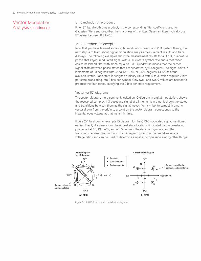
BT, bandwidth time product
Filter BT, bandwidth time product, is the corresponding filter coefficient used for Gaussian filters and describes the sharpness of the filter. Gaussian filters typically use BT values between 0.3 to 0.5.
Measurement conceptsNow that you have learned some digital modulation basics and VSA system theory, the next step is to learn about digital modulation analysis measurement results and trace displays. The following examples show the measurement results for a QPSK, quadrature phase shift keyed, modulated signal with a 50 ksym/s symbol rate and a root raised cosine baseband filter with alpha equal to 0.35. Quadrature means that the carrier signal shifts between phase states that are separated by 90 degrees. The signal shifts in increments of 90 degrees from 45 to 135, –45, or –135 degrees. QPSK has four available states. Each state is assigned a binary value from 0 to 3, which requires 2 bits per state, translating into 2 bits per symbol. Only two I and two Q values are needed to produce the four states, satisfying the 2 bits per state requirement.
Vector (or IQ) diagrams
The vector diagram, more commonly called an IQ diagram in digital modulation, shows the recovered complex, I-Q baseband signal at all moments in time. It shows the states and transitions between them as the signal moves from symbol to symbol in time. A vector drawn from the origin to a point on the vector diagram corresponds to the instantaneous voltage at that instant in time.
Figure 2-11a shows an example IQ diagram for the QPSK modulated signal mentioned earlier. The IQ diagram shows the 4 ideal state locations (indicated by the crosshairs) positioned at 45, 135, –45, and –135 degrees, the detected symbols, and the transitions between the symbols. The IQ diagram gives you the peak-to-average voltage ratios and can be used to determine amplifier compression among other things.
Vector diagramor IQ diagram
(a) QPSK
90ϒ
0ϒ (phase ref)
• Symbols
• State locations
• Decision points
I
Q
Constellation diagram
270ϒ
90ϒ
180ϒ180 ϒ 0 ϒ (phase ref)
270 ϒ
Symbol trajectorybetween states
11 10
0001
Q
I
Symbols outside thecircle exceed error limits
11 10
0001
(b) QPSK
–1 v
–1 v
–1 v
–1 v
Figure 2-11. QPSK vector and constellation diagrams
Vector Modulation Analysis (continued)
32 | Keysight | Vector Signal Analysis Basics - Application Note
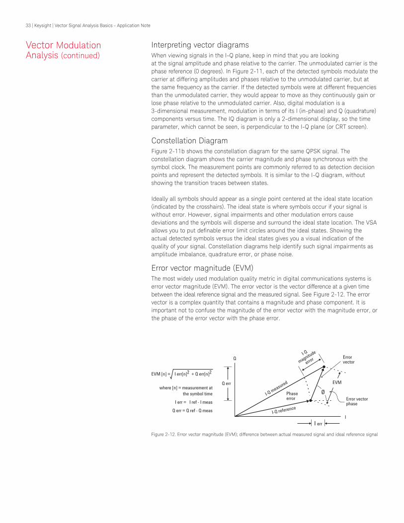
Interpreting vector diagramsWhen viewing signals in the I-Q plane, keep in mind that you are looking at the signal amplitude and phase relative to the carrier. The unmodulated carrier is the phase reference (0 degrees). In Figure 2-11, each of the detected symbols modulate the carrier at differing amplitudes and phases relative to the unmodulated carrier, but at the same frequency as the carrier. If the detected symbols were at different frequencies than the unmodulated carrier, they would appear to move as they continuously gain or lose phase relative to the unmodulated carrier. Also, digital modulation is a 3-dimensional measurement, modulation in terms of its I (in-phase) and Q (quadrature) components versus time. The IQ diagram is only a 2-dimensional display, so the time parameter, which cannot be seen, is perpendicular to the I-Q plane (or CRT screen).
Constellation DiagramFigure 2-11b shows the constellation diagram for the same QPSK signal. The constellation diagram shows the carrier magnitude and phase synchronous with the symbol clock. The measurement points are commonly referred to as detection decision points and represent the detected symbols. It is similar to the I-Q diagram, without showing the transition traces between states.
Ideally all symbols should appear as a single point centered at the ideal state location (indicated by the crosshairs). The ideal state is where symbols occur if your signal is without error. However, signal impairments and other modulation errors cause deviations and the symbols will disperse and surround the ideal state location. The VSA allows you to put definable error limit circles around the ideal states. Showing the actual detected symbols versus the ideal states gives you a visual indication of the quality of your signal. Constellation diagrams help identify such signal impairments as amplitude imbalance, quadrature error, or phase noise.
Error vector magnitude (EVM)The most widely used modulation quality metric in digital communications systems is error vector magnitude (EVM). The error vector is the vector difference at a given time between the ideal reference signal and the measured signal. See Figure 2-12. The error vector is a complex quantity that contains a magnitude and phase component. It is important not to confuse the magnitude of the error vector with the magnitude error, or the phase of the error vector with the phase error.
where [n] = measurement at the symbol time
I err = I ref - I meas
Q err = Q ref - Q meas
EVM [n] = I err[n]2 + Q err[n]2
I err
Q err
Q
I-Q reference
I-Q measured
Errorvector
EVM
Phaseerror
I-Q
magnitude
error
Error vectorphase
Ø
I
Figure 2-12. Error vector magnitude (EVM); difference between actual measured signal and ideal reference signal
Vector Modulation Analysis (continued)
33 | Keysight | Vector Signal Analysis Basics - Application Note

EVM is defined as the root mean square (rms) of the error vector over time at the instants of the symbol clock transitions. By convention, EVM is usually normalized to either the amplitude of the outermost symbol or the square root of the average symbol power. The EVM measurement and the various related data results are sensitive to any signal impairment that affects the magnitude and phase trajectory of a signal for any digital modulation format. This makes it an ideal measurement tool for troubleshooting communications system problems at baseband, IF, or RF sections of the radio.
Figure 2-13 shows examples of the error vector time, error vector spectrum, I-Q magnitude error, and I-Q phase error modulation quality measurements that were defined in Figure 2-12. The error vector time data (display a) shows the error vector magnitude data in the time domain. This trace is the computed error vector magnitude between corresponding symbol points in the I-Q measured and I-Q reference signals. The error vector spectrum data (display b) shows the spectrum of the error vector time data. In other words, the analyzer derives the error vector time data, and then windows and FFTs this data to produce the error vector spectrum trace. This format can reveal the spectral content of the unwanted signals that drive the modulated carrier away from its ideal path. If those error components are deterministic, they will show up in the error vector spectrum trace as spectra. Measuring these spectra can give added insight into the nature and origin of these error signals. The I-Q magnitude error (display c) and I-Q phase error (display d) traces show the error between the I-Q measured and the I-Q reference signals. I-Q magnitude error displays the magnitude error and I-Q phase error displays the phase error.
Figure 2-13. Display a, error vector time, shows the error vector magnitude at the symbol points. Display b, error vector spectrum, shows the frequency spectrum of the error vector time data. Display c, IQ mag error, is the magnitude difference between the measured and reference IQ waveforms. Display d, IQ phase error, is the phase difference between the measured and reference IQ waveforms.
Vector Modulation Analysis (continued)
34 | Keysight | Vector Signal Analysis Basics - Application Note

Symbol table/error summary
The symbol table/error summary measurement results may be the most powerful of the digital demodulation tools. Here, demodulated bits can be seen along with error statistics for all of the demodulated symbols. For example, reviewing the rms EVM value can quickly help you assess modulation accuracy. Other valuable errors are also reported. Figure 2-14 shows the symbol table/error summary data for the QPSK signal used previously. The marker readout shows the values for the highlighted bits in the symbol table, which represent symbol number 3 and has a value of 2 (a binary value of “10”). Note that this agrees with the two bits per symbol required by QPSK modulation. The errors table shows the available statistical and error data for a QPSK modulated signal.
We have now covered some of the fundamental modulation measurements, but there are many more qualitative displays and quantitative measurements available. You can find more information about them in the References section at the end of this application note.
Vector Modulation Analysis (continued)
Figure 2-14. The symbol table/error summary data provides the demodulated bits and error statistics for all the demodulated symbols
35 | Keysight | Vector Signal Analysis Basics - Application Note
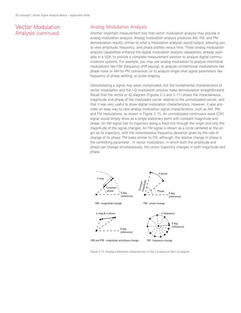
Analog Modulation AnalysisAnother important measurement tool that vector modulation analysis may provide is analog modulation analysis. Analog modulation analysis produces AM, FM, and PM demodulation results, similar to what a modulation analyzer would output, allowing you to view amplitude, frequency, and phase profiles versus time. These analog modulation analysis capabilities enhance the digital modulation analysis capabilities, already avail-able in a VSA, to provide a complete measurement solution to analyze digital commu-nications systems. For example, you may use analog modulation to analyze intentional modulations like FSK (frequency shift keying), to analyze unintentional modulations like phase noise or AM-to-PM conversion, or to analyze single-shot signal parameters like frequency or phase settling, or pulse shaping.
Demodulating a signal may seem complicated, but the fundamental characteristics of vector modulation and the I-Q modulation process make demodulation straightforward. Recall that the vector or IQ diagram (Figures 2-2 and 2-11) shows the instantaneous magnitude and phase of the modulated carrier relative to the unmodulated carrier, and that it was very useful to show digital modulation characteristics. However, it also pro-vides an easy way to view analog modulation signal characteristics, such as AM, PM, and FM modulations, as shown in Figure 2-15. An unmodulated continuous wave (CW) signal would simply show as a single stationary point with constant magnitude and phase. An AM signal has its trajectory along a fixed line through the origin and only the magnitude of the signal changes. An FM signal is shown as a circle centered at the ori-gin as its trajectory, with the instantaneous frequency deviation given by the rate of change of its phase. PM looks similar to FM, although, the relative change in phase is the controlling parameter. In vector modulation, in which both the amplitude and phase can change simultaneously, the vector trajectory changes in both magnitude and phase.
Constant phase
AM - magnitude change
0 deg(reference)
Phase
PM - phase change
AM and PM - magnitude and phase change FM - frequency change
Δ frequency
Cons
tant
mag
nitu
de
Δ phase
Δ mag & Δ phase
0 deg(reference)
Δ mag
0 deg(reference)
0 deg(reference)
Figure 2-15. Analog modulation characteristics in the I-Q plane on the I-Q diagram
Vector Modulation Analysis (continued)
36 | Keysight | Vector Signal Analysis Basics - Application Note

Traditionally, to view the carrier modulation waveforms (modulation envelope), you would remove the carrier by “detecting” and displaying the resultant waveform on an oscilloscope in amplitude-versus-time display. However, instead of thinking in terms of detecting the modulation on the carrier, in vector modulation, it is helpful to think of viewing the modulation as what is left after the carrier has been “shifted” or “downconverted” to 0 Hz. An intuitive review of frequency shifting will show how amplitude and phase changes imparted on the carrier are “detected” using basic trigonometric identities
As shown in Figure 2-16, the complex-modulated carrier signal, described by V(t) = A(t)Cos[2πfct + Ø(t)] and frequency, fc, are inputted to the quadrature mixer (or quadrature detector) for frequency translation. To recover the baseband modulating signal, the carrier is first downconverted to baseband (0 Hz) by setting the LO frequency equal to fc. Then the baseband signals are low-pass filtered so only the difference frequencies remain. This process produces real I(t) and imaginary Q(t) time-domain waveforms that are the magnitude and phase difference between the modulated carrier signal and the unmodulated LO signal, referenced to the carrier. This is the carrier modulation in the form of I(t) and Q(t) components (rectangular coordinates), not in terms of magnitude, A(t), and phase, Ø(t). You may recall that the I-Q demodulator performs a polar to rectangular conversion. However, applying some math and simple trigonometric identities to the I(t) and Q(t) components allows us to extract the instantaneous amplitude, A(t), or phase, Ø(t), changes impressed on the carrier. This is the AM and PM modulation.
real part
Imaginary part
90Quadrature
Ø(t) = Phase
Detected PM = Ø(t) = tan–1 [Q(t)/I(t)] Detected AM = A(t) = I2(t ) + Q2 (t)
FLO = fcLocal oscillatorModulated carrier fc
Incident
Detected FM = Derivative of PM = dØ/dt Quadrature detector (I-Q demodulator)
V(t) = A(t) Cos [ 2π fct + Ø(t)]
A(t) Cos [ 2π fct + Ø(t)]
Cos [ 2π fct]
–Sin [ 2π fct]
The modulated carrier is described by: AM FM & PM
where A(t) = Magnitude
I(t)
Q(t)
Figure 2-16. Modulation is measured by shifting the carrier frequency, fc, down to 0 Hz. When the digital LO frequency is equal to the modulated carrier frequency, the output of the quadrature detector, I(t) and Q(t) time-domain waveforms, is the modulation on the carrier
Vector Modulation Analysis (continued)
37 | Keysight | Vector Signal Analysis Basics - Application Note

The amplitude modulation, AM, is the variation of the carrier magnitude, A(t), versus time and is extracted from I(t) and Q(t) by taking the square root of the sum of the squares of I(t) and Q(t).
AM = A(t) = sqrt[I2(t) + Q2(t)]
Phase modulation, PM, is the phase variation, Ø(t), versus time and is equal to the arct-angent of [Q(t) / I(t)]. Frequency modulation, FM, is the derivative of the phase shift verses time, dØ/dt. That is, FM is the derivative of PM:
PM = Ø(t) = arctan[Q(t)/I(t)]
FM = derivative of the PM = (dØ/dt)
Starting with I(t) and Q(t) and applying basic trigonometric identities, we have done a first order demodulation of the carrier and are able to look at AM, PM, and FM modula-tion. In practice, analyzers use sophisticated demodulation algorithms that incorporate frequency and phase error correction routines so that intentional and unintentional modulation can be accurately separated from the carrier. Analog demodulation com-pletely isolates the PM and FM from the AM. Likewise, AM is completely isolated from the PM and FM.
SummaryThis chapter presented the basics of vector or digital modulation techniques and digital modulation analysis as implemented in a vector signal analyzer. We described digital (vector or I-Q) modulation and common digital modulation formats. The VSA architec-ture is similar to a digital communication system so we described the radio receiver and transmitter block diagrams noting the process of generating, transmitting, receiving and recovering the original digital information. We then looked at the VSA digital demodulator block and described each function and the related demodulation parame-ters necessary to properly demodulate your signal and make measurements. The VSA, with vector modulation analysis, provides powerful and specialized measurement capa-bility that allows you to characterize and troubleshoot throughout the entire block dia-gram of a digital system (system using I and Q signals). The information you learned in this chapter will help you make informed decisions regarding measurement instrumen-tation requirements and the tools necessary to analyze your communication system. Vector modulation analysis is also available on swept-tuned spectrum analyzers that support additional radio personality software.
The scope of this application note is limited to the fundamental concepts. If you would like more in-depth information, you can review the suggested reference materials in the References section at the end of this application note.
Vector Modulation Analysis (continued)
38 | Keysight | Vector Signal Analysis Basics - Application Note
1. Robert A Witte. Spectrum and Network Measurements. Atlanta, GA: Noble Publishing Corporation, 2001
2. Keysight Technologies, The Fundamentals of Signal Analysis, Application Note 243, literature number 5952-8898E, Palo Alto, CA, July 1978.
3. Keysight Technologies, Using Vector Modulation Analysis in the Integration, Troubleshooting and Design of Digital RF Communications Systems, Application Note 89400-8, literature number 5091-8687E, Palo Alto, CA, July 1994.
4. Keysight Technologies, Digital Modulation in Communications Systems - An Introduction, Application Note 1298, literature number 5965-7160E, Palo Alto, CA, July 1997.
5. Keysight Technologies, Testing and Troubleshooting Digital RF Communications Transmitter Designs, Application Note 1313, literature number 5968-3578E, Palo Alto, CA, July 1999.
6. Keysight Technologies, Testing and Troubleshooting Digital RF Communications Receiver Designs, Application Note 1314, literature number 5968-3579E, Palo Alto, CA, July 2002.
References
39 | Keysight | Vector Signal Analysis Basics - Application Note

40 | Keysight | Vector Signal Analysis Basics - Application Note
This information is subject to change without notice.© Keysight Technologies, 2017Published in USA, December 1, 20175989-1121ENwww.keysight.com
This documnet was formerly Application Note 150-15.
www.keysight.com/find/spectrumanalyzers
For more information on Keysight Technologies’ products, applications or services, please contact your local Keysight office. The complete list is available at:www.keysight.com/find/contactus
Americas Canada (877) 894 4414Brazil 55 11 3351 7010Mexico 001 800 254 2440United States (800) 829 4444
Asia PacificAustralia 1 800 629 485China 800 810 0189Hong Kong 800 938 693India 1 800 11 2626Japan 0120 (421) 345Korea 080 769 0800Malaysia 1 800 888 848Singapore 1 800 375 8100Taiwan 0800 047 866Other AP Countries (65) 6375 8100
Europe & Middle EastAustria 0800 001122Belgium 0800 58580Finland 0800 523252France 0805 980333Germany 0800 6270999Ireland 1800 832700Israel 1 809 343051Italy 800 599100Luxembourg +32 800 58580Netherlands 0800 0233200Russia 8800 5009286Spain 800 000154Sweden 0200 882255Switzerland 0800 805353
Opt. 1 (DE)Opt. 2 (FR)Opt. 3 (IT)
United Kingdom 0800 0260637
For other unlisted countries:www.keysight.com/find/contactus(BP-9-7-17)
DEKRA CertifiedISO9001 Quality Management System
www.keysight.com/go/qualityKeysight Technologies, Inc.DEKRA Certified ISO 9001:2015Quality Management System
Evolving Since 1939Our unique combination of hardware, software, services, and people can help you reach your next breakthrough. We are unlocking the future of technology. From Hewlett-Packard to Agilent to Keysight.
myKeysightwww.keysight.com/find/mykeysightA personalized view into the information most relevant to you.
http://www.keysight.com/find/emt_product_registrationRegister your products to get up-to-date product information and find warranty information.
Keysight Serviceswww.keysight.com/find/serviceKeysight Services can help from acquisition to renewal across your instrument’s lifecycle. Our comprehensive service offerings—one-stop calibration, repair, asset management, technology refresh, consulting, training and more—helps you improve product quality and lower costs.
Keysight Assurance Planswww.keysight.com/find/AssurancePlansUp to ten years of protection and no budgetary surprises to ensure your instruments are operating to specification, so you can rely on accurate measurements.
Keysight Channel Partnerswww.keysight.com/find/channelpartnersGet the best of both worlds: Keysight’s measurement expertise and product breadth, combined with channel partner convenience.