king fahd university of petroleum & minerals college of computer
TRANSCRIPT

1
King Fahd University Of Petroleum & Minerals
College Of Computer Science & Engineering
Computer Engineering Department
COE 400
Digital System Design
Lab Manual
Prepared By:
Muhammad Wasim Raad
With the Help of Mr. Masud-ul-Hasan

2
Preface
About The Manual: The digital system design course emphasizes major concepts of embedded applications which satisfy the main system design components which are: application domain, software component, and hardware component. In the context of designing a full digital system, the design strategy focuses on using state of the art intelligent controllers or microcontrollers usually available in modern embedded applications in addition to all parallel and serial interface standards with host PCs or workstations. The embedded applications put some constraint on the design like portability, low power consumption, cost-effectiveness, real-time computation, and compliance with international standards. In the context of the project design, students are exposed to project design techniques and development design tools, engineering design methods, Design tradeoffs. The students are required to work in groups, and to be able to design & implement a full fledge computer engineering project which integrates all of the knowledge the student has accumulated from other courses, in addition to allowing students to practice the design experience in a real commercial like project. The main computing engine chosen for the target hardware is the 8051 core microcontroller family and its variants because of its simplicity & excellent support available on this processor. Each semester a different project is given. This lab manual has been specifically designed to support the target project in the form of a number of experiments. The experiments form a dynamic structure of the different modules of the total project, but they were designed such that they will provide the students with the necessary hardware & software background. Since the course aims at designing & implementing a digital system design in the wide sense, taking advantage of the state of the art advances in computer applications & digital system design, some flexibility has been added to the experiments such that they are upgradeable. Some experiments emphasize hardware and some other emphasize software & others concentrate on using available tools like simulators/debuggers or microcontroller programmers. All relevant data sheets & applications notes are put into one appendix at the end of the lab manual. Students are trained throughout the lab how to use the data sheets in their design. A new development tool (hardware and software) has been acquired recently including an advanced 8051 microcontroller for automotive applications (80C515), in addition to Read51 software which includes an assembler, C compiler, and editor, linker, debugger and chip simulator. The tool also includes a simple real-time multithreading kernel for real-time embedded applications. The development system includes also a reconfigurable CPLD for fast prototyping.

3
Some Guidelines for the Students
• Do not put the power on while making the connections in your prototyping board. • Use universal standard color coding of wires for VCC and GND i.e., RED for VCC
and Black for GND. • Make sure to always wear the anti-static wrist strap while dealing with the chips. • Make sure to take good care of the tools and chips which are given to you. • Make sure to always back up your working directory in the PC and keep good
documentation of your project. • Make sure to leave your table neat and equipment in their proper place and switch off
all equipment except the PC before you leave. • Do not bring tea or coffee or any other drink to your working station. • If you use the solder iron make sure you leave it on the stand and do not leave it
hanging some where else because that might cause fire or endanger your colleagues. • If you suspect any equipment on your table is missing report that to the instructor
right away.

4
Sample project
Term Project
A Smart Card-Based Remote Home Control & Hazard detection System with additional E-Commerce & intruder warning feature
The project aims at designing & building a smart card –based remote home control & hazard detection system to allow a person to control any home appliance in his home remotely and securely by using a smart card (nothing but a credit-like card with an 8051 on it for encryption and decryption) which can be plugged into one of the available COMs of a PC. The other COM should be connected remotely through a serial cable or a modem to a controller board based on the 8051 for controlling the various home appliances and for monitoring emergency events like a fire hazard or an unwanted intruder. The PC should have a visual basic environment running showing a virtual home on the PC screen allowing an authorized user to enter his home by inserting his personal smart card, and once the VB completes the operation of verifying the authenticity of the smart card and the user through a PIN (personal identification number), it should grant him access to enter any room put off or on lights, turn on hi- fi or start the microwave oven to cook his favorite food by click of a button. In case of emergency like a fire or an intruder entering the house or even the garage door opening during night an alarm should be activated in addition to some animation on the screen showing location of emergency. The system should also have a time & date stamp feature for saving the time & date any body enters the house. The system should have an e-commerce feature by allowing the user to enter an airline or a shopping site and purchase his ticket on-line using his smart card and pay using cash stored on his smart card & download the ticket on his smart card. A loyalty feature gives customers special benefits like free tickets or discounts on shopping. The smart card should be fabricated on a printed circuit board on the smallest scale possible. Protel1.5 or an equivalent PCB cad tool can be used to draw the PCB layout of the designed smart card. Cash can be downloaded on an EEPROM on the smart card. If a user tries to use a fake smart card or try to hack the system, the system should block him from accessing the house in the future. The system should have some allowance for limiting children from using the smart card to access dangerous facilities at home like the microwave oven or playing with the emergency detection system. For hazard or intruder detection, sensors such as reed switches and infra red sensors or other kind of sensors are recommended.

5
Optional (Bonus#1): Making the application web based. Optional (Bonus#2): Building the home controller on a small PCB. Optional (Bonus#3): Adding an infra-red connection to the smart card. Optional (Bonus#4): Using the PC modem for remote home control Optional (Bonus#5): Adding a wireless control (RF) link to the controller like a home door chime or similar. A well documented final report (both hard copy and electronic format) should be submitted along with the project at the end of the semester. The instructors of both sections will select best project from each section as well as the most distinguished individual for the course award. Additional bonus will be given to any student who contributes to the COE 400 homepage by adding any useful information related to the course in addition to contributions to the course in terms of tutorials or any relevant material. A certificate of appreciation will be given to each student at the end of the course indicating the main skills & expertise he learned and obtained from the course.

6
Sample project
Term Project
A Smart Card Based Remote Industrial Oil Monitoring & control system with an emergency warning & Hazard control feature
The project aims at designing an industrial standard & robust intelligent oil monitoring system capable of detecting emergency levels of oil in different oil production sites. The system should be able to report to a remote PC situated couple of kilometers away status of the oil and in case of any leakage through a serial link or using leased modem lines or Ethernet. There will be one microcontroller unit attached to oil tanks which will send warning messages to remote PC in case of emergency in addition to activating local alarm. The microcontroller should be capable of tuning on or off the oil valve based on a remote command from the main PC. The site also should be protected against hazards like fire or intruders by installing the necessary hazard or intruder detectors. The main PC should have a VB environment, animating cont inuously the oil filling and distribution process in addition to icons for directly controlling the oil valve or switching lights off remotely. Other processes in the site like loading oil into truck should be possible to automate. The person in charge however cannot access the main computer unless he inserts a smart card (built around an 8751 or flash microcontroller+ EEPROM) into one of the available COMS of the PC. The smart card should start authentication process with the PC along with requesting the user to enter a PIN (Personal Identification Number) which is 4 to 5 digits long. In case the user enters a wrong PIN three times the smart card will be blocked and will only be unblocked upon entering a PUK (PIN Unblocking Key) issued from the service provider for one time only. The smart card should have also loyalty feature for customers who wish to buy oil products from the site online, by adding points for future discount or other privileges. The smart card should be designed as small as possible and should be secure enough to be hacker proof, and should be built on a Printed Circuit board. The design features are left open to satisfy a cost effective robust and secure design guidelines. The system should have an email emergency or maintenance request warning feature when an emergency occurs at the site, by sending an email to site manager with a full maintenance or emergency report. The smart card should have the feature of activating a modem dialer once it finishes authentication to connect with other sites to share information about site status. A time and date stamp feature should also be available whereby whenever somebody enters the site during night his entrance should be time and date stamp.

7
A full comprehensive final report should be prepared + electronic copy. The smart card should be encapsulated in a protective cover + an installation guide and full software on a CD. Optional: Web enabled design and marketing research (BONUS). Note: Emphasis in project evaluation is based on functionality, robustness of design, noise immunity, and portability of product, cost effectiveness and novel ideas in hardware or software. Tradeoffs in design between hardware or software solutions for example should be considered.

8
EXP#1 Basic Module of 8051
Objective: To learn how to build a working 8051 basic module. Background: Intel offers a family of microcontrollers, including the 8-bit 8048, 8049, 8031 and 8051.
The 8031 contains 128 bytes of RAM, and 32 I/O lines. Added to that, two 16-bit timers
which provide accurate real- time recording of events. The 8031 also has a full duplex
serial I/O port.
Main Features of the 8031 / 8051:
- 4 Kbytes of internal ROM for the 8051 only
- 128 bytes of RAM.
- Four 8-bit I/O ports.
- Two 16-bit timers.
- Serial interface.
- 64K external code memory space.
- 64K external data memory space.
- Boolean processor (operates on single bit).
- 210-bit addressable locations.
- Four microseconds multiply/divide.
Procedure:
Build a stand alone 8051 module as explained in the lecture using external EPROM and a latch. Test the RESET circuit using Oscilloscope. Do the necessary connections on a prototype board as shown in figure 1. In the following figure (Figure 1) is the interface of the 8031 with the 2716 EPROM and
the clock and the reset circuitry. Note that because the EPROM capacity is 2K = 211, 11

9
ports are needed from the 8031. Thus ports P0.0 to P0.7 are used in addition to P2.0 to
P2.2. These 11 ports are first connected to the SN74LS373N Buffer and then to the
EPROM. This is because the 8031 does not have the sufficient current to drive the
EPROM. Make sure you know how to solve the design problem of expanding the
memory capacity of your microcontroller board and the kind of decoding needed.
Figure 1 shows schematic of interfacing 8051 to external EPROM
Components Needed:
1. 8031 Microcontroller (one) 2. 74373 Latch (one) 3. 2716 EPROM (one) 4. 12 MHz Crystal (one) 5. 10 µf Capacitor (one) 6. 100Ω and 8kΩ Resistor (one each) 7. Push Button (Reset Switch) 8. Bread Boards (two) 9. Wires (at least 3 colors) 10. 40 Pin Socket (one)
8051
PORT2
ALE
PORT0
PSEN
ADDRESS LATCH
ROM(S)
ADDRESS INPUTS
DATA OUTPUTS
OE
A15 - A8
A7 - A0
D7 - D0
AD7 - AD0
EA

10
EXP#2
Working Module of 8051
Objective: To learn how to program an 8051 based working module using PC-based programmer. Get acquainted with 8051 debugger/simulator 1.9 beta, assembler, linker, debugger, and programmer. Background: The shareware simulator used is a user friendly simulator/debugger which is window based and has many versatile features like break points, simulating interrupts, EPROM, RAM, I/O ports, registers, and a very powerful dummy terminal for simulating serial communication, along with the capability to change program on the fly. See below a screen shot of it. Procedure: Test the 8051 module built in experiment #1 by burning square wave generator examples from chapter 4 (i.e., Example 4-1, 4-3, 4-4) in Mackenzie book. You should verify that you get the right waveform by using an oscilloscope. Familiarize yourself with using the simulator/debugger on the examples mentioned above.
Components: Programmer, Oscilloscope

11

12
EXP #3
Using the 8051 timers to Create Different Delays
Objective: To learn how to generate different delays using 8051 timers. Background: The 8051 microcontroller has two 16 bit timers used either as timers for generating preprogrammed time delays or as counters for counting external events. The timers go at a rate 1/12 of the crystal rate and can be used either for generating time delays or to overflow and generate interrupt driven applications.
Procedure:
Familiarize yourself with how to use the 8051 timers and initialize them to generate different time delays. Burn the following two programs on EPROM; the output is measured using oscilloscope to verify the generated frequency with the correct duty cycle. Modify example 4-4 to give a delay of 5 seconds. Also make sure you know how to design a code with the minimum timing error possible by making your code as efficient as possible & how interrupts supercede polling to achieve this goal.
A 10KHZ square wave require wave require a high time of 50µs and a low time of 50µs, since this interval less than 256 µs, timer mode 2 can be used.

13
EXAMPLE 4-2 ORG 0000
MOV TMOD, #02H ; 8 BIT TIMER MODE MOV TH0, #0FFH ; 50 RELOAD VALUE SETB TR0 ; START TIME LOOP: JNB TF0, LOOP ; WAIT FOR OVERFLOW CLR TF0 ; CLEAR TIMER OVERFLOW FLAG CPL P1.0 ; TOGGLE PPORT BIT SJMP LOOP ; REPEAT END
A 1KHZ square wave requires a high-time of 500µs and low-time of 500µs. Since this interval is longer than 256µs, so for that we use full 16 bit timer mode or mode 1. EXAMPLE 4-4 ORG 0000 MOV TMOD, #01H LOOP: JNB P1.6, LOOP WAIT: JB P1.6, WAIT SETB P1.7 CALL DELAY CLR P1.7 SJMP LOOP ; DELAY: MOV R7, #100 AGAIN: MOV TH0, #D8H MOV TL0, #F0H SETB TR0 WAIT2: JNB TF0, WAIT2 CLR TF0 CLR TR0 DJNZ R7, AGAIN RET END
Components: Oscilloscope, prototyping breadboard

14
EXP#4
Using the 8051 to control DC & AC devices with different delays using Timer interrupts
Objective: To learn how to control DC & AC devices using an 8051 based module. Background: Microcontrollers are control oriented devices equipped with very powerful single bit instructions capable of context switching of devices interfaced to them. Since these microcontrollers are CMOS, usually buffers and transistors are needed to increase there driving capability to drive DC or AC devices. The most popular power transistors used are the Darlington pair transistors. Make yourself familiar with the concept of an electro- magnetic relay and the different kinds of relays. Conduct a search on all kinds of relays used in industry and select the most suitable for your application. Understand how a transistor drives a relay and the purpose of putting the diodes across the relay. The figure below shows a circuit for driving the relay using a transistor. The relay is a single pole relay.
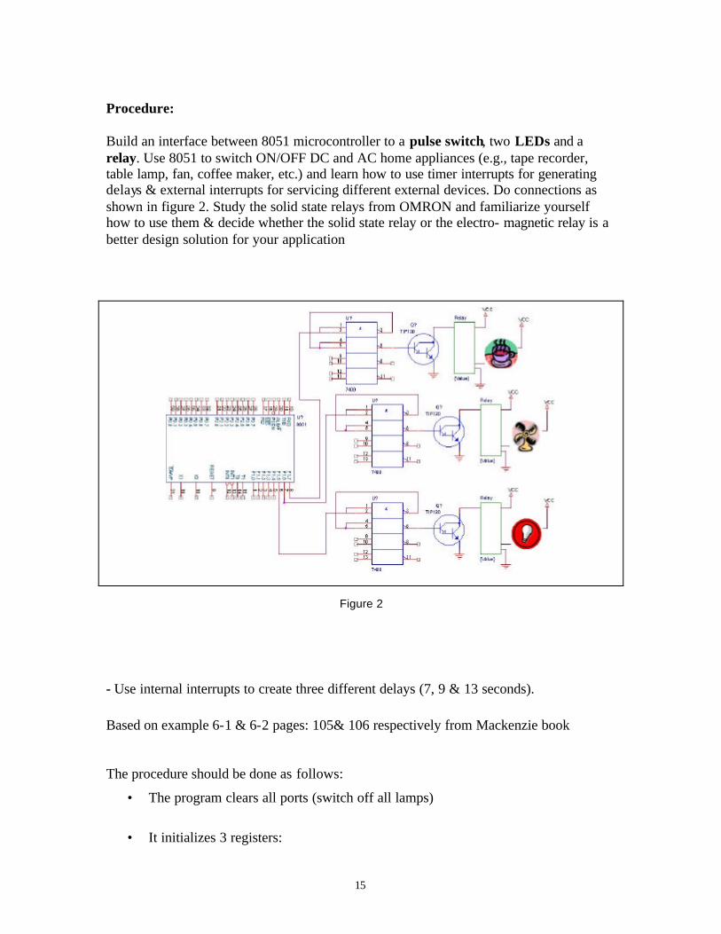
15
Procedure: Build an interface between 8051 microcontroller to a pulse switch, two LEDs and a relay. Use 8051 to switch ON/OFF DC and AC home appliances (e.g., tape recorder, table lamp, fan, coffee maker, etc.) and learn how to use timer interrupts for generating delays & external interrupts for servicing different external devices. Do connections as shown in figure 2. Study the solid state relays from OMRON and familiarize yourself how to use them & decide whether the solid state relay or the electro- magnetic relay is a better design solution for your application
Figure 2
- Use internal interrupts to create three different delays (7, 9 & 13 seconds). Based on example 6-1 & 6-2 pages: 105& 106 respectively from Mackenzie book The procedure should be done as follows:
• The program clears all ports (switch off all lamps)
• It initializes 3 registers:

16
§ R1 = 10610
§ R2 = 13710
§ R2 = 19810
Also timer0 in mode1 (16 bits) with 0000H so it goes to FFFFH (= 216) 10
To achieve the (7, 9 & 13) delays, the calculation is done as follows:
§ 106 3216 = 6949816 ≈ 7000,000 µs = 7s
§ 137 3216 ≈ 9s
§ 198 3216 ≈ 13s
• When an interrupt takes place, the ISR is called. The timer is stopped.
Then the registers are decremented and then compared to Zero, if not the
timer is loaded then sited on, then return to the main program till next
routine. If any register is Zero then the port is coupled accordingly. Then
the register is reloaded with its value and so on.
The waveform of the circuit is shown below:
7s 7s
9s 9s
13s 13s

17
Components needed:
• 2 6V Relays.
• 2 (2-input NAND gates) ICs
• 2 TIP120 or121 Darlington Pair Transistors.
• One lamp.
• One magnetic reed switch.
• One fan.
• One buzzer.
• Diode 9001
Note: Refer to RS catalogue for data sheet of transistors

18
EXP #5 Intruder alarm using reed relays
Objective: To be able to use a reed relay as an example of an external interrupt which interrupts the microcontroller in the case of an intruder opening the door to activate an alarm for a pre-specified time, and get to know how to interface it with the microcontroller. To be able to program the priority of two external interrupts for two different doors. Background: A reed switch or relay is basically just two small pieces of springy metal that overlap one another. These pieces of metal are the “reeds” and are normally fitted in a glass envelope. The reeds are spaced slightly apart so that they are not quite in electrical contact with
each other. If a reasonably strong bar magnet is placed next to a reed switch, the two reeds become temporarily magnetized by the field of the magnet. The two ends of the reeds that are in close proximity to each other have opposite poles, and accordingly they are attracted to one another. This results in the overlapping ends moving together and touching, so that electrical contact is completed. These gives simple switching action, with the switch open when the magnet is absent, and close when it is brought close to the reeds. The magnet must be across with the reed switch to operate (i.e. the magnet is placed at 90 degrees with the reed switch). Procedure: Connect the reed switch as shown in the Figure 1 (a) to 5V, resistor and GND and the output to microcontroller external interrupt pin such that when the reed switch closes a high to low pulse is applied to the microcontroller to invoke the external interrupt and activate the alarm. Put the magnet on one side of the door and the reed switch aligned to it such that when the door opens the reed switch closes. Design your interface circuit to comply with a negative-edged triggered interrupt or negative- level triggered. Conduct a search on all of the available reed switches in the market and study their specifications to decide which is the most suitable for your application. Familiarize yourself with other intruder alarm sensors like laser detector or infra red detector and how to interface it to your microcontroller. Circuit of Figure 1 (a) gives a negative edge while Figure 1 (b) gives a positive edge.

19
Figure 1
Components: Two reed switches, two magnets, alarm horn, power supply & breadboard. Sample program:
ORG 0000H LJMP MAIN ORG 0003H LJMP EX0ISR ORG 0013H LJMP EX1ISR ;
MAIN: SETB IT0 ; negative edge activated MOV TMOD, #11H ; 16 bit timer mode MOV IE, # 81H ; Enable Ext0 interrupt only SJMP $ ; infinite loop ;
EX0ISR: SETB TF0 ; force timer 0 interrupt SETB TF1 ; force timer 1 interrupt SETB ET0 ; begin tone for 1 second SETB ET1 ; enable timer interrupts SETB P1.7 ; intruder alarm for the first door RETI ;
EX1ISR: SETB P1.6 ; intruder alarm for the second door RETI

20
EXP#6
AC devices control
Objective: To get the students familiarized how to deal with AC devices Background: When you want to choose an AC appliance for control, make sure you know its power rating. Divide power rating by operating AC voltage and you will ge t the current rating permissible. If current rating of relay is larger or equal to device current rating then you can use the device safely, otherwise find a larger relay. Procedure: Familiarize yourself with three phase AC concept and how the connections are done. See the figure shown below. Make sure you understand how the ac devices are interfaced to the microcontroller. Use an ac device to control using the microcontroller. Enhance your design by adding some safety measures to your circuit like an optoisolator to protect against a short circuit or large current, study all components used for this purpose. Assume you are required to use your AC board for controlling AC devices like a coffee Maker or a washing machine or an oscilloscope, what certain factors you should consider and on what criteria you choose your relays. Come up with an optimum design for such an application.

21
Components used: -AC board with 6 device sockets and their corresponding relays -A multi-meter - CD ROM catalogues

22
EXP#7
Serial Communication Using 8051 Microcontroller
Objective: To learn how to use the serial port and interrupts of 8051 microcontroller. To learn how to use RS232 serial port of PC. Background: RS232 is the standard communication protocol supported by IBM PCs and giving capability to communicate up to a distance of 100M using low capacitance cables and with good noise screening. The 8051 is equipped with a full duplex UART which can communicate serially up to 115K baudrate. Because of the RS232 positive & negative logic, a voltage level converter is needed which converts from RS232 logic level to TTL logic. The output signal usually swings between +12V and –12V, >+3V=0 logic and > -3V=1 logic. We use the MAX232 or MAX233 to do the voltage conversion to TTL & because they are single supply drivers. Refer to Appendix I Procedure:
Connect the necessary hardware make sure you use the right serial cable between PC & microcontroller. Burn program-1 shown below on the EPROM using interrupts to continually transmit the ASCII code set (excluding control codes) to the PC Hyper terminal. Make sure you learn how to set up configuration of the hyper terminal such that the baud rate and protocol complies with the configuration programmed on the 8051. See a screenshot of hyper terminal configuration below. You can use also the COM debug utility available on the shared folder.There are 95 graphic codes (20H to 7EH) out of total 128 ASCII codes. Modify the program to receive characters from a remote hyper terminal or VB program and echo back the characters. Allow for a preset buffer in your program to receive a full string using lookup table technique explained previously in the lecture. Conduct a study on all of the serial design solutions available including RS485, USB, CAN… and decide which is best to use for your project from the performance point of view & noise immunity.

23

24
Program-1: ORG 0 LJMP MAIN ORG 0023H LJMP SPISR ORG 0030H MAIN: MOV TMOD, #20H MOV TH1, #-26 SETB TR1 MOV SCON, #42H MOV A, #20H MOV IE, #90H SJMP $ SPISR: CJNE A, #7FH, SKIP MOV A, #20H SKIP: MOV SBUF,A INC A CLR TI RETI END Components Needed:
- MAX 232 - 5 Capacitors (0.1 µf each) - Serial cable attached to a terminal/PC - Solder type DB9 - Null modem serial cable
Note: Refer to appendix for data sheets of MAX232 & DB9

25
EXP#8
Basic Module of 8051 on PCB
Objective: To learn how to design and fabricate a PCB for 8051 basic module. Background: Most printed circuit board manufacturing is done by putting the pattern of circuit traces and pads onto a sheet of copper-clad phenolic or fiberglass board using substances that will resist the action of copper-etching solutions. This can be done by directly drawing on a board with a resist pen or by a photographic process where the portions of a board that are struck by ultraviolet light passing through a negative image of traces become, following development, resistant to etchant. A new and relatively easy method is the use of special sheets of material on which a circuit design can be printed with a laser printer or photocopier, after which the pattern is transferred to a copper board . Please note that developing and etching PCBs is a process that involves chemicals that can burn your skin, have hazardous neurotoxic fumes, can be absorbed into your bloodstream, and cannot be disposed of without powered ventillation . Procedure:
1) Design the final product: using Protel program, we design the layout of the
Smart Card PCB in one level layout. In this step, the designer should check the
design several times before he starts the implementation of the design in the
board.
2) Photographic section: This part involves placing the complete (working) layout
of the circuit onto a transparency by using the camera (repromaster camera). After
the transparency is exposed it is developed. Editing of the finished layout comes
next. Making sure that all tracks are complete and pads are covered.

26
3) Transferring Transparency layout onto PCB : Using UV machine, the
transparency is exposed onto the PCB for a fixed amount of time. The exposed
PCB is then developed so that the design (layout) appears on the PCB. Again one
must edit the PCB to make sure that all tracks are complete and pads are covered.
Once that is done, the PCB is placed in the “etching” solution (FeCO2 – Ferric
Chloride) to remove the unwanted copper. Cleaning and drying the PCB follows.
4) Tin Plating Process: This step is needed for a more efficient soldering process.
Since tine and the lead (soldering material) stick together better than copper and
lead. Tin also gives a thicker, protective track on the PCB over the copper.
5) Cutting and Soldering : Once the board is completely dry, it is cut to its intended
size. The components are then soldered on according to the layout.
Components needed to put on the PCB are the following:
- 8751 Microcontroller (40 pins) - MAX 233 (16 pins) - EEPROM (8 pins) - Voltage Regulator 7805 (3 pins) - 11.059 MHz Crystal (2 pins) - Power Socket (2 pins) - DB9 Socket (9 + 2 pins) - 100Ω and 8kΩ Resistors and 1 Capacitor for Reset (2 pins each) - Push Button (Reset Switch 2 pins) - Noise filtering capacitors (2 pins each)
Note: Connect EA pin to VCC.

27
EXP#9 Infra Red Sensor
Objective: To be able to use a intra red as an example of an external interrupt which interrupts the microcontroller in the case of an object is cutting the light of the infra red sensor. Then, try to program stop device and active another device. Background: An infra red sensor is basically just a sender terminal and receiver terminal. These two objects are connected through a circuit shown in figure 1. The two objects are far from each other (maximum distance = 10 maters). The output of the sensor is 0V if any object comes through the infra red it gives 5V. Procedure: In the figure, the transmitter is connected to a resistor (200? ) to give more transmission rate(as the resistor decrease the transmission increase) and for the receiver it is connected (to switch it on the resistor should be high(1M? )) when there is any object passing between the transmitter and the receiver it gives logic 1, but because it gives low current we connect to buffer to give more current and then to a NOT Gate to give a negative edge within passing any object through the infra red. The output of the not gate is connect to the microcontroller.
a bMicrocontrollerP .
+ V+ V
Transmitter Reciver
BufferNOT Gate
Ohm M Ohm
Components: Two resistors (200? and 1M?), transmitter & receiver, buffer, NOT gate, power supply & breadboard.

28
Exp#10
PWM DC motor /light Dimmer control
Objective: To learn how to control DC motor speed/direction
Background:
A pulse width modulator (PWM) is a device that may be used as an efficient light dimmer or DC motor speed controller. Pulse Width Modulation (or PWM) is a simple way to modulate, or change, a square wave. In its basic form, the duty cycle of the square wave is changed according to some input. The duty cycle is the ratio of high and low times in the square wave. A 50%/50% duty cycle would be high for 50% of the time and low for 50% of the time. Likewise, a 10%/90% duty cycle would be high for 10% and low for 90%.
The circuit shown in Yeralan book is a general purpose device that can control DC devices which draw up to a few amps of current. This device has been used to control the level of intensity for the lamp and as a motor speed control for small DC fans of the type used in computer power supplies.
A PWM circuit works by making a square wave with a variable on-to-off ratio, the average on time may be varied from 0 to 100 percent. In this manner, a variable amount of power is transferred to the load. The main advantage of a PWM circuit over a resis tive power controller is the efficiency, at a 50% level, the PWM will use about 50% of full power, almost all of which is transferred to the load, a resistive controller at 50% load power would consume about 71% of full power, 50% of the power goes to the load and the other 21% is wasted heating the dropping resistor.
One additional advantage of pulse width modulation is that the pulses reach the full supply voltage and will produce more torque in a motor by being able to overcome the internal motor resistances more easily. Finally, in a PWM circuit, common small potentiometers may be used to control a wide variety of loads whereas large and expensive high power variable resistors are needed for resistive controllers.
There are many applications for PWM including motor control, servo control, light dimming, switching power supplies, and even some audio amplifiers. The program below shows how can we use assembly to handle speed control of DC motor as well as light dimming:

29
TURN LIGHT ON "0%" MOV R3,#0 MOV R4,#-1 ; MOV A,#32H LCALL OUTCHR JMP TMPXT "75% " CJNE A,#33H,LHDM2 MOV R3,#-20 MOV R4,#-60 MOV A,#33H LCALL OUTCHR JMP TMPXT ; "50% " CJNE A,#34H,LHDM3 MOV R3,#-40 MOV R4,#-40 MOV A,#34H LCALL OUTCHR JMP TMPXT ; "25% " CJNE A,#35H,LHOF MOV R3,#-60 MOV R4,#-20 MOV A,#35H LCALL OUTCHR JMP TMPXT ; "0% " CJNE A,#36H,C1 MOV R3,#-1 MOV R4,#0 MOV A,#36H LCALL OUTCHR JMP TMPXT Refer to the circuit diagram shown in figure 5.13 on page 215 in Yeralan book for using PWM to control speed of DC motor. The same circuit can be used for light dimming by substituting the DC motor with a lamp. The RC circuit at the input acts like a low pass filter or a DAC ( Digital to Analogue ) converter to control the intensity of current flowing through the DC motor coil. Procedure:
1- Build the PWM circuit described above and assemble and link and execute the program listed above to generate different duty cycles at port 1.0 of the microcontroller, and hence different DC motor speeds.

30
2- Use appropriate bias voltage for the DC motor. 3- Verify the correct operation of the DC motor speed control. 4- Refer to the circuit below for controlling direction of DC motor and on/off modes usinf one
DPDT relay and another SPDT relay. 5- Build the circuit and verify its correct operation. 6- Make sure you understand the concept of DC motor direction control using DPDT relays.
Components: • DC motor or halogen lamp • A darlington power transistor • NPN low power transistor • DPDT 6V electromechanical relay • SPDT 6V electromechanical relay • 1K resistor • 1 uF capacitor • 1000 uF capacitor • flywheel diode

31
EXP #11
Reading & Writing to an EEPROM Objective: To be able to write to a serial EEPROM & read from it remotely Background: 1) EEPROM or E2PROM Program
Write Operations : Before any write or read operation, the X24C02 (slave) must
receive a start condition from the Microcontroller (master). The start condition, is a
HIGH to LOW transition of the SDA while the SCL is HIGH. The X24C02 continuously
monitors the SDA line for this condition. After the start condition the master device must
then issue a slave address indicating the slave device it is to interface and the type of data
transfer required (write or read). In the case of the X24C02, the device type identifier is
fixed as 1010B. Because only one E2PROM is used in this arrangement, then the address
bits are grounded. Once the start condition and the slave address is received by the
X24C02, it sends an acknowledgement (ACK) on the SDA lines. Now the master
continuously polls the SDA lines for the ACK. For Write conditions, the E2PROM
requires another address field indicating the address of the location that the data is to be
written on the X24C02. Again after the transmission of this word address, the slave must
send an ACK which is sensed by the master. Finally the data itself is sent on the SDA
lines once the word address is acknowledged by the X24C02. Once the data is sent and
acknowledged, the master must then transmit a stop bit indicating the end of
communication. The stop condition is a LOW to HIGH transition of SDA when the SCL
is HIGH.
2) Read Operation: The write operation is very similar to the read operation.
However, a sort of trick is employed in order to specify an address within the X24C02 to
be read. A dummy write operation is indicated initially by giving the start condition and
the slave address with the R/W bit set for a write operation. Once the ACK is received by

32
the master, the word address required is transmitted to the X24C02. When the ACK for
that word address is received, another start condition is issued with the R/W bit set for a
read operation. This technique is used to be able to control which address is used for
reading data. Following the ACK of the second start bit and the second slave address, the
data from the word address specified will be on the SDA lines. A stop bit is then issued
by the master, indicating the end of communication.
Procedure: Use the echo serial routine (refer to: Programming and Interfacing the 8051 Microcontroller book, by: Sencer Yeralan, p:176-178) to send a number from the hyper- terminal to store it on the EEPROM & echo it back to the screen. You can also use the programmer to program the EEPROM or verify if information has been written successfully to it. Study the EEPROM data sheet & application note carefully and make sure to understand the serial protocol used. Design the necessary interfacing circuitry between the 8051 microcontroller & the serial EEPROM used. Components needed: Serial EEPROM like X24C02 or X24C04.
Note: You should refer to EEPROM data sheet & application note in the appendix.

33
EXP#12
VB programming
Objective: To design a secure & user friendly VB environment to communicate with the remote hardware using COM1 & COM2 serial ports & to develop the VB according to the requirements of the specific project given Background:
The purpose of the high- level program, using Visual Basic in this project, is to establish communication between the PC terminal and the other devices. This communication is performed through the MSComm32.OCX, which is one of the ActiveX components that provide an interface to a standard set of communications commands. It allows you to establish a connection to a serial port, connect to another communication device (e.g. a modem) issue commands, exchange data, and monitor and respond to various events and errors that may be encountered during a serial connection.1
There are many functions which are supposed to be performed by the high- level language (Visual Basic) in this project and they are:
1- The communication function.
2- The authentication and security function.
3- The controlling function.
1-The Communication Function
As it’s described previously, the VB can establish the serial communication through the COM Ports (Every computer comes with one or more serial ports. They are named successively: COM1, COM2, and so on. On a standard PC, the mouse is usually connected to the COM1 port. A modem may be connected to COM2, a scanner to COM3, etc. Serial ports provide a channel for the transmission of data from these external serial devices. The essential function of the serial port is to act as an interpreter between the CPU and the serial device. As data is sent through the serial port from the CPU, Byte values are converted to serial bits. When data is received, serial bits are converted to Byte values) 1. There are two ways of handling this communication:

34
A- Event-driven communications:
This is a very powerful method for handling serial port interactions. In many situations, you want to be notified the moment an event takes place, such as when a character arrives or a change occurs in the Carrier Detect (CD) or Request To Send (RTS) lines. In such cases, use the MsComm control's OnComm event to trap and handle these communications events.
B- Polling communication:
Events can be handled after a specific event happen. For example, if you are writing a simple phone dialer, it may not make sense to generate an event after receiving every character, because the only characters you plan to receive are the OK response from the modem.
Procedure: Edit & compile the following program which establish node to node chatting using MSCOMM events & opens a text box & verify that the communication is successful. Develop your VB to add icons related to devices you want to control as needed & familiarize yourself with using the timer in VB plus additional features like animation which can give excellent real time feedback of the status of the remote hardware. Private Sub cmdExit_Click() MSComm1.PortOpen = False End End Sub Private Sub cmdSend_Click() MSComm1.Output = Text1.Text Text1.Text = "" End Sub Private Sub Form_Load() MSComm1.PortOpen = True Form2.Show End Sub Private Sub MSComm1_OnComm() Text2.Text = Text2.Text + MSComm1.Input End Sub The following code shows how to program the day & time in VB: Private Sub Form_Load() txtMonth.Text = Month(Date) txtDay.Text = Day(Date)

35
txtYear.Text = Year(Date) txtDate.Text = Date End Sub Private Sub Timer1_Timer() txtTime.Text = Time txtMin.Text = Minute(Time) txtHour.Text = Hour(Time) txtSec.Text = Second(Time) End Sub Private Sub txtMonth_Change() End Sub Private Sub txtTime_Change() End Sub Figure 3 shows the form that will appear on the screen for send & receive.
Figure 3. VB form for send & receive using MSCOMM The following is a sample program in VB how to use polling for receiving messages
sent from another PC or microcontroller:
private Sub cmdExit_Click() MSComm1.PortOpen = False End End Sub Private Sub Form_Load() Form1.Show Form2.Show MSComm1.PortOpen = True Do DoEvents Text1.Text = Text1.Text + MSComm1.Input Loop Until MSComm1.Input = "/" End Sub

36
Notes on how to design your project: 1- Read very well the project description and make sure to understand the main
requirements of the project. 2- Each group should meet regularly with the group leader and use brain storming to
put solutions to the main design problem 3- Use charts and detailed documentation to record the different relevant details needed
in designing your project. 4- Identify the main hardware & software modules needed and the leader should assign
each member a job related to these modules 5- Make your design modular such that each module is self testable ( a module could
be one or more experiments). 6- Extend the modularity approach to your software design including the high level as
well as the low level. 7- Make sure that there is complete synchronization between the high level on the PC
and the low level on the microcontroller. 8- Use software tools like simulators to debug your software continuously . 9- Establish a logic criteria for integrating the different modules of the project and a
testing criteria to verify the conformity of your design with the initial specifications & requirements of the project.
10. Design your final product on a PCB optimizing the space to get the smallest & most
efficient design 11. Document your project on a full fledge report with an electronic copy included 12. Point out the main innovations in the projects along with any useful suggestions

37
The following figure shows a sample project:
(Figure 5)
Main.frm
Smart Card
Microcontroller Board
Fire alarm Laser sensor
Credit is displayed.
Rest emergency VB and Devices
Open log file
Display members of the team and system info
Fire and intruder interrupt.
ON/OFF Device

38
The main.frm is the main screen. It is used to control all the devices and monitor the fire and intruder alarm. This from is only used when the user is fully verified. The following is a screen shot of how a smart card authenticating protocol is designed in one of the projects in VB: