kit912s812ecuevm small engine reference design · kit912s812ecuevm small engine reference design,...
TRANSCRIPT

NXP SemiconductorsUser’s guide
Document Number: KT912_S812ECUUGRev. 3.0, 3/2016
© 2016 NXP B.V.
KIT912S812ECUEVM small engine reference designFeaturing the MM912_S812 MCU and ignition/injector driver system-in-package
Figure 1. KIT912S812ECUEVM reference design board

KIT912S812ECUEVM small engine reference design, Rev. 3.0
2 NXP Semiconductors
Table of Contents
1 Kit contents/packing list . . . . . . . . . . . . . . . . . . . . . . . . . . . . . . . . . . . . . . . . . . . . . . . . . . . . . . . . . . . . . . . . . . . . . . . . . 3
2 Jump start . . . . . . . . . . . . . . . . . . . . . . . . . . . . . . . . . . . . . . . . . . . . . . . . . . . . . . . . . . . . . . . . . . . . . . . . . . . . . . . . . . . 4
3 Important notice . . . . . . . . . . . . . . . . . . . . . . . . . . . . . . . . . . . . . . . . . . . . . . . . . . . . . . . . . . . . . . . . . . . . . . . . . . . . . . . 5
4 Introduction . . . . . . . . . . . . . . . . . . . . . . . . . . . . . . . . . . . . . . . . . . . . . . . . . . . . . . . . . . . . . . . . . . . . . . . . . . . . . . . . . . 6
5 Exploring the contents of KIT912S812ECUEVM . . . . . . . . . . . . . . . . . . . . . . . . . . . . . . . . . . . . . . . . . . . . . . . . . . . . . . 7
6 Recommended additional hardware. . . . . . . . . . . . . . . . . . . . . . . . . . . . . . . . . . . . . . . . . . . . . . . . . . . . . . . . . . . . . . . 11
7 System setup . . . . . . . . . . . . . . . . . . . . . . . . . . . . . . . . . . . . . . . . . . . . . . . . . . . . . . . . . . . . . . . . . . . . . . . . . . . . . . . . 12
8 Application development . . . . . . . . . . . . . . . . . . . . . . . . . . . . . . . . . . . . . . . . . . . . . . . . . . . . . . . . . . . . . . . . . . . . . . . 19
9 System overview . . . . . . . . . . . . . . . . . . . . . . . . . . . . . . . . . . . . . . . . . . . . . . . . . . . . . . . . . . . . . . . . . . . . . . . . . . . . . 28
10 Application overview . . . . . . . . . . . . . . . . . . . . . . . . . . . . . . . . . . . . . . . . . . . . . . . . . . . . . . . . . . . . . . . . . . . . . . . . . . 29
11 Schematic . . . . . . . . . . . . . . . . . . . . . . . . . . . . . . . . . . . . . . . . . . . . . . . . . . . . . . . . . . . . . . . . . . . . . . . . . . . . . . . . . . 31
12 Board layout . . . . . . . . . . . . . . . . . . . . . . . . . . . . . . . . . . . . . . . . . . . . . . . . . . . . . . . . . . . . . . . . . . . . . . . . . . . . . . . . . 35
13 Bill of materials . . . . . . . . . . . . . . . . . . . . . . . . . . . . . . . . . . . . . . . . . . . . . . . . . . . . . . . . . . . . . . . . . . . . . . . . . . . . . . . 39
14 Appendix A: hardware reference manual . . . . . . . . . . . . . . . . . . . . . . . . . . . . . . . . . . . . . . . . . . . . . . . . . . . . . . . . . . . 42
15 Appendix B: software reference manual . . . . . . . . . . . . . . . . . . . . . . . . . . . . . . . . . . . . . . . . . . . . . . . . . . . . . . . . . . . 54
16 References. . . . . . . . . . . . . . . . . . . . . . . . . . . . . . . . . . . . . . . . . . . . . . . . . . . . . . . . . . . . . . . . . . . . . . . . . . . . . . . . . . 59
17 Revision history . . . . . . . . . . . . . . . . . . . . . . . . . . . . . . . . . . . . . . . . . . . . . . . . . . . . . . . . . . . . . . . . . . . . . . . . . . . . . . 60
KIT912S812ECUEVM small engine reference design, Rev. 3.0
NXP Semiconductors 3
Kit contents/packing list
1 Kit contents/packing list
• Assembled and tested KIT912S812ECUEVM board in anti-static bag. • ECU wire harness• USB BDM Tool• 6-pin ribbon cable• A-to-B USB cable• Warranty card

KIT912S812ECUEVM small engine reference design, Rev. 3.0
4 NXP Semiconductors
Jump start
2 Jump start
• Go to www.nxp.com/analogtools• Locate your kit• Review your tool summary page• Look for
Jump Start Your Design
• Download documents, software, and other information

KIT912S812ECUEVM small engine reference design, Rev. 3.0
NXP Semiconductors 5
Important notice
3 Important notice
NXP provides the enclosed product(s) under the following conditions:
This evaluation kit is intended for use of ENGINEERING DEVELOPMENT OR EVALUATION PURPOSES ONLY. It is provided as a sample IC pre-soldered to a printed circuit board to make it easier to access inputs, outputs, and supply terminals. This EVB may be used with any development system or other source of I/O signals by simply connecting it to the host MCU or computer board via off-the-shelf cables. This EVB is not a Reference Design and is not intended to represent a final design recommendation for any particular application. Final device in an application will be heavily dependent on proper printed circuit board layout and heat sinking design as well as attention to supply filtering, transient suppression, and I/O signal quality.
The goods provided may not be complete in terms of required design, marketing, and or manufacturing related protective considerations, including product safety measures typically found in the end product incorporating the goods. Due to the open construction of the product, it is the user's responsibility to take any and all appropriate precautions with regard to electrostatic discharge. In order to minimize risks associated with the customers applications, adequate design and operating safeguards must be provided by the customer to minimize inherent or procedural hazards. For any safety concerns, contact NXP sales and technical support services.
Should this evaluation kit not meet the specifications indicated in the kit, it may be returned within 30 days from the date of delivery and will be replaced by a new kit.
NXP reserves the right to make changes without further notice to any products herein. NXP makes no warranty, representation or guarantee regarding the suitability of its products for any particular purpose, nor does NXP assume any liability arising out of the application or use of any product or circuit, and specifically disclaims any and all liability, including without limitation consequential or incidental damages. “Typical” parameters can and do vary in different applications and actual performance may vary over time. All operating parameters, including “Typical”, must be validated for each customer application by customer’s technical experts.
NXP does not convey any license under its patent rights nor the rights of others. NXP products are not designed, intended, or authorized for use as components in systems intended for surgical implant into the body, or other applications intended to support or sustain life, or for any other application in which the failure of the NXP product could create a situation where personal injury or death may occur.
Should the buyer purchase or use NXP products for any such unintended or unauthorized application, the buyer shall indemnify and hold NXP and its officers, employees, subsidiaries, affiliates, and distributors harmless against all claims, costs, damages, and expenses, and reasonable attorney fees arising out of, directly or indirectly, any claim of personal injury or death associated with such unintended or unauthorized use, even if such claim alleges that NXP was negligent regarding the design or manufacture of the part. NXP™ and the NXP logo are trademarks of NXP Semiconductors. All other product or service names are the property of their respective owners. © 2016 NXP B. V.

KIT912S812ECUEVM small engine reference design, Rev. 3.0
6 NXP Semiconductors
Introduction
4 Introduction
Welcome to the NXP small engine reference design kit. This product was designed to be a complete solution for the electronic control of a small engine. Small engines are defined as a one or two cylinder engine for use in anything from a motorbike to a lawn mower to a generator. While the decision was made to address a one-cylinder engine specifically, this design is extremely useful for a two-cylinder engine with little or no modification. NXP's concept of creating an engine control kit is intended to enable a market ranging from garage hobbyist to seasoned Tier 1 powertrain engineer using NXP products.
Through the use of this kit, you can create an engine controller specific to a small engine application. Engine control is a discipline that requires intimate knowledge and experience in chemical, mechanical, and electrical engineering. For those familiar with mechanical control of an engine through a carburetor, the use of this reference design kit can help to advance your knowledge in the electrical area and provide a jump-start for a successful adoption of electrical engine controls to meet new emissions standards. Providing a kit such as this is intended to make semiconductor products from NXP easier to use. The user is responsible for providing all input signals, output loads as well as the completed system design and development. This kit should serve as a starting point for the development of an application specific engine controller for a small engine. Example software and documentation are provided to assist in successful design and implementation. It is recommended to have the following skills and experience: embedded C-language programming, analog and digital circuit design, and schematic analysis, microcontroller programming, fuel injection system debugging and calibration, and engine test environment experience. Additionally, there is further benefit to experiencing the CodeWarrior Development Studio and the NXP S12X microcontroller Units (MCUs). The user reference manual provides exercises and references to additional information to reduce the learning curve for inexperienced users.
NXP's goal is to enable the small engine market. To clarify this point, the hardware included in this kit can readily be configured and reprogrammed to run an engine. However, it lacks the application specific hardening (EMC, ESD, and environmental areas for example) and implementation optimization that make it a production ready module for any specific application. Further, the free example application software provided is a starting point capable of running an engine. It does not apply any advanced control strategy capable of addressing the pollution concerns and regulations facing the small engine industry. To do this would become application specific to an engine and could not be and should not be implemented by a semiconductor supplier as it is deeply outside their area of expertise. The example application software does show how to use the key functionality in the NXP products that the kit is based on, which speeds up the development process by showing a working example.
The contents of this kit saves many months of work, even for experienced powertrain engineers just looking to evaluate NXP products. A system was created based on a one-cylinder closed-loop engine controller using integrated technology while being cost-effective for the small engine market. Example software is provided that can be customized to run an actual engine that has electronic fuel injection. Documentation is provided to aid in going through the process of developing an application. Finally, information on modifying the design to support the adaptation of the small engine reference design to your application goals.

KIT912S812ECUEVM small engine reference design, Rev. 3.0
NXP Semiconductors 7
Exploring the contents of KIT912S812ECUEVM
5 Exploring the contents of KIT912S812ECUEVM
Included in this kit are the essential components to develop an engine control application for small engines. Development is centered on the use of a Windows based PC and the electronic control unit (ECU) contained in this kit. The key components of the kit are: ECU, wire harness, NXP CodeWarrior for the S12X (part of the jump start software/documentation bundle that can be downloaded from www.nxp.com/analogtools), USB BDM tool, and USB cable. Refer to the packing list for any additional components which may be included in the kit. If any of the contents are missing, use the included warranty card or contact your local NXP support team.
5.1 Electronic control unit (ECU)
This is the small engine reference design hardware. It is a one-cylinder engine controller based on the NXP MM912JS812 which contains a MC9S12XS128 microcontroller and an MC33812. The unit runs from a 12 V battery and control engine loads such as a fuel injector, inductive ignition coil, relays, incandescent lamps, and LEDs. The ECU also takes inputs from switches and sensors, such as engine stop switch, manifold air pressure, engine temperature, and variable reluctance sensors. Application software implementing the engine control strategy is run on this unit. The unit is not designed to be a production module specific to any particular engine; rather, it is intended to work with many different types. This resulted in the small “business-card” form factor and limited options for expansion.
12-pin signal connectorsecondary side
16-pin load connectorsecondary side
IGBT ignitiondriver
MC33879 configurableoutput driver
Additional discretepower drivers
CAN protocolinterface
MM912_S812S12XS MCU
BDM programmingand debugging port
VRSconditioning
circuit
Figure 2. ECU included in KIT912S812ECUEVM
5.1.1 ECU board features• MM912JS812 SiP• VRS sensor conditioner• Fuel pump driver• Idle speed motor driver• HEGO heater driver• CAN interface• IGBT ignition coil driver• I/O connectors• BDM connector• Reverse battery and transient protection• +5.0 V regulator external PNP transistor

KIT912S812ECUEVM small engine reference design, Rev. 3.0
8 NXP Semiconductors
Exploring the contents of KIT912S812ECUEVM
5.1.2 MM912JS812 SiP features
The MM912JS812 system in a package (SiP) contains the MC9S12XS128 and MC33812 ICs. The MC9S12XS128 is an optimized 16-bit automotive microcontroller focused on low cost, high-performance, and low pin-count. This microcontroller is targeted at generic automotive applications requiring CAN or LIN/J2602 communication. The MC9S12XS128 has the following features:
• S12 CPU core• 128 kbyte on-chip flash with ECC• 4.0 kbyte DataFlash® with ECC• 8.0 kbyte on-chip SRAM• Phase locked loop (IPLL) frequency multiplier with internal filter• 4.0 to 16 MHz amplitude-controlled Pierce oscillator• 1.0 MHz internal RC oscillator• Timer module (TIM) supporting input/output channels providing a range of 16-bit input capture, output compare, counter,
and pulse accumulator functions• Pulse width modulation (PWM) module with 8-channel x 8-bit or 4-channel x 16-bit• 16-channel, 12-bit resolution successive approximation analog-to-digital converter (ADC)• One serial peripheral interface (SPI) module• One serial communication interface (SCI) module supporting LIN communications• One multi-scalable controller area network (MSCAN) module (supporting CAN protocol 2.0A/B)• On-chip voltage regulator (VREG) for regulation of input supply and all internal voltages• Autonomous periodic interrupt (API)
The MC33812 is an engine control analog power IC intended for motorcycle and other single/dual cylinder small engine control applications. The IC consists of three integrated low-side drivers, one pre-driver, a +5.0 V, voltage pre-regulator, an MCU watchdog circuit, an ISO 9141 K-Line interface, and a parallel interface for MCU communication.
• Designed to operate over the range of ~4.7 V ≤ VPWR ≤ 36 V• Fuel injector driver - current limit - 4.0 A typical• Ignition pre-driver can drive IGBT or Darlington bipolar junction transistors• Ignition pre-driver has independent high-side and low-side outputs• Relay driver - current limit - 4.0 A typical• Lamp driver- current limit - 1.5 A typical• All external outputs protected against short to battery, overcurrent• Ignition and other drivers protected against overtemperature• Interfaces directly to MCU using 5.0 V parallel interface• VCC voltage pre-regulator provides +5.0 V power for the MCU• MCU power on RESET generator• MCU watchdog timer circuit with parallel refresh/time setting line• Independent fault annunciation outputs for ignition, injector and relay drivers• ISO-9141 K-Line transceiver for communicating diagnostic messages
NXP analog ICs are manufactured using the SMARTMOS process, a combinational BiCMOS manufacturing flow that integrates precision analog, power functions and dense CMOS logic together on a single cost-effective die.
5.2 ECU wire harness
To provide a physical connection to the electronic fuel injection system, a wired connection to the controls and sensors of the system is required. As a starting point, a basic wire harness is included in the kit along with the components to fully populate the connectors. The basic wire harness allows power to be applied to the module and a minimal set of loads. Later in this manual, there is documentation discussing the process of interfacing the signals of the engine to the ECU. Additional connectors can be easily obtained through known electronic component suppliers. Exact part numbers are made available in the bill of materials (BOM) for the ECU.

KIT912S812ECUEVM small engine reference design, Rev. 3.0
NXP Semiconductors 9
Exploring the contents of KIT912S812ECUEVM
Figure 3. ECU wiring harness
5.3 Jump start software/documentation bundle
The documentation media contains electronic copies of all relevant information for creating and using this kit, including this user manual. Documentation includes various support tools, such as spreadsheet tools, and design files including schematics and Gerber output files. These can be accessed through the graphical application automatically launched or by using Windows Explorer as a more direct navigation of the contents. For the latest relevant information, refer to www.nxp.com/analogtools.
5.4 NXP CodeWarrior for the S12X
All firmware for the ECU is developed using this development software, which is included in the software/documentation bundle. This is done as a convenience as it is a large program to download. It is recommended to check for the latest version and updates at www.nxp.com. The CodeWarrior development studio is an integrated development environment providing a common interface for working with the various tools needed for building software. It comes in various levels of product for various types of MCUs. The example software allows the use of the special edition product which is free for use. As your application grows and further features of the product are required, upgraded licenses can be purchased to meet your needs. The primary function of the CodeWarrior application is to compile software, program the ECU, and then control the execution of the software through the integrated debugger.
Figure 4. Screen shot of NXP CodeWarrior for the S12X

KIT912S812ECUEVM small engine reference design, Rev. 3.0
10 NXP Semiconductors
Exploring the contents of KIT912S812ECUEVM
5.5 USB BDM tool
Connection from the Windows PC to the ECU is performed by the USB-to-BDM Tool. This tool is powered through the USB port and interfaces with the CodeWarrior application. The link to the ECU is through a six-pin ribbon cable going from the USB BDM tool to the background debug module (BDM) header on the ECU. Through the BDM connection, the CodeWarrior application can use the BDM tool to communicate, program, and control the S12 microcontroller on the ECU. While the tool gets its power from the USB port on the PC, it does not power the ECU. This separation is important as it provides a level of isolation from the engine system to the development PC. This kit makes use of the TBDML. It is important to know which tool you are using so the proper connection is selected when using CodeWarrior.
Figure 5. Example USB BDM tool for connection to PC
KIT912S812ECUEVM small engine reference design, Rev. 3.0
NXP Semiconductors 11
Recommended additional hardware
6 Recommended additional hardware
In addition to this kit, various pieces of equipment are recommended to perform application development work for software validation and testing. These are commonly found in most electronics labs:
• 12 V, 10 A DC power supply• 100 MHz (minimum) four channel oscilloscope• Soldering iron• Grounded electrostatic matt• Windows XP/7 PC• 12 V relays• Potentiometers• Switches.
Having all of these items allow system testing and debugging.

KIT912S812ECUEVM small engine reference design, Rev. 3.0
12 NXP Semiconductors
System setup
7 System setup
Since contents of the small engine reference design kit have been described, the focus can shift to the complete development system. This includes the contents of this kit and the fuel injected engine as a system. At a high level, system setup contains the following steps:
• Definition of interface between ECU and engine• Creation of simulated engine environment• Installation and verification of software development environment• Engine load and sensor validation• Migration plan towards real engine hardware
To accomplish these steps, several exercises are described to help take the user through this critical phase. These exercises include, getting started with NXP CodeWarrior, and creating a known reference system. Additionally, suggestions for further training are provided based on using NXP products and the system level setup. Figure 6 shows the components of this kit and a placeholder for the engine. This system incorporates the interface from the PC to the actual engine. The user must provide the engine loads for electronic fuel injection, including fuel injector, inductive ignition coil, relays, and other relevant components. Signals from VRS, MAP, switches, and other inputs must also be provided with the actual engine itself.
Software development on PC USB Connection to ECU
engineWire harness forconnection to EFIsystem
Small engine ECU
Figure 6. KIT912S812ECUEVM board setup

KIT912S812ECUEVM small engine reference design, Rev. 3.0
NXP Semiconductors 13
System setup
7.1 Definition of the interface between ECU and engine
The first step in using this kit is to determine how it connects to the engine system. As mentioned, the engine must be fuel injected. If converting an engine from mechanical (carburetor) to electronic control, this must be done before or in parallel with using this kit. The ECU is designed around a one-cylinder engine, however, it can be adapted to work with a two-cylinder engine. The requirements for two-cylinder operation are: a) ignition coil must be a dual output or twin coil, b) wasted-spark strategy is acceptable for application. This means a twin coil, capable of driving two separate spark plugs from a single input, can be used to fire every engine revolution (in a four-stroke engine) to produce two spark events, one in the desired cylinder and one in the second (wasted) cylinder. If this can be tolerated in the system, fuel control can be provided individually to each cylinder through the INJOUT and ROUT1 signals.
To aid in the connection from the ECU to the engine, a worksheet is provided. Using load worksheet.xls, available on the documentation CD, connection to the engine can be defined. This Excel spreadsheet contains the full list of connections and suggested functionality for each pin of the ECU. Matching up the various controls, sensors, and inputs on the engine to the ECU should take into account voltage ranges and current capabilities. If there is any doubt to the connection, use the information found in Appendix A: hardware reference manual for in-depth analysis of the circuits behind each ECU level pin.
The design goal of a cost-efficient design does not allow for a system to include all possible system configurations. The signals available reflect essential controls for one-cylinder, closed-loop engine control, highlighting the integration of the MM912JS812AMAF small engine IC. Essential functionality should be considered first, such as the direct controls for fuel and spark. System controls such as the fuel pump or voltage regulator should be of secondary concern as they can be externally controlled and do not require precise timing execution.
By filling in the information under the “target engine system” column, see the yellow highlight in Engine load worksheet - target system identification column in yellow, each connection to the ECU can be defined. In the actual worksheet, signals of the ECU are color coded to identify similar functionality. From this completed worksheet, the wire harness from the engine to the ECU can be made. Materials for the AMP brand connectors of the ECU are included to get this process started.
Engine load worksheet - target system identification column in yellow
Exercise 1: Complete the load worksheet for the target engine system.
1. Open “load worksheet.xls” and bring the “instructions” sheet to the front by clicking on this tab.
2. Collect information such as wiring diagrams and schematics for the engine system to be run.
3. Use the engine system information to define how each signal of the ECU is going to be connected to the engine. This includes a definition of an existing pin on a connector, wire color and type, and the functionality associated with the system. This table is also useful for configuring the software.
4. Repeat this exercise for creating a simulated engine environment.
KIT912S812ECUEVM reference design Target engine system
Connector Pin Signal name
Signal type
Voltage range
Recommended Functionality Connector pin Wire color Functional description
1 VPWR Power input
13.6 V System power from 12 V battery
2 ISO9141 Input/ output
0-VBAT Bi-directional communication pin for diagnostics
3 COIL 0-VBAT Spark control of digital ignition system
4 GND 0 V Module level ground reference, return path of VBAT
5 GND 0 V Module level ground reference, return path of VBAT
6 TPMD 0-VBAT H-bridge control for four-phase stepper motor for idle speed air speed control

KIT912S812ECUEVM small engine reference design, Rev. 3.0
14 NXP Semiconductors
System setup
7.2 Creation of simulated engine environment
Before the simulated environment can be created, the ECU must have a viable power source. As the ECU is designed to work in a real engine system, it is required to have a 12 V power source. A power supply capable of generating 12 V at 1.0 A is a good starting point for the ECU alone. Depending on the loads to be connected to the ECU, a much larger power supply may be required with higher current. A good starting point for working with a full featured system is a 12 V, 10 A power supply. While the total system loads may be greater, 10 A is generally large enough since the high current loads of ignition and injectors are not typically on simultaneously.
The best and safest way to begin developing an application for engine control is to work with a simulated engine system. This reduces risk and development time by not having to focus on fuel related safety concerns when trying to solve arising complex applications issues. Developing with a simulated engine system engine begins by selecting components similar or identical to the actual components on the engine. For many of the loads, these can be the exact same components. In some cases, loads can be replaced by a lesser expensive relay or a light. Relays work well for high power loads with dynamic operating frequencies such as ignition and injectors. In those cases, the sound of the relay actuation is beneficial to validate behavior during low speed testing. Other loads work better with lights or LEDs. These are more simple loads simply controlled as on or off for long periods of time. Some loads require the actual load to test, such as an idle speed motor.
Perhaps the most challenging part of the system to simulate is engine position. Two core technologies are used to sense engine position: variable reluctance sensors (VRS) and Hall Effect sensors. The majority of production engines use a VRS for engine position. The advantage of the VRS is cost, while a Hall Effect sensor provides a cleaner output signal. Both types are supported on the ECU. The default configuration is for VRS. Use the schematic to identify the components to remove and populate for using a Hall Effect sensor.
With respect to creating a simulated engine environment, engine position is the fundamental element. Simulating the rotation of the engine can be done in two ways, virtual and physical simulation. A virtual simulation involves a digital re-creation of the spinning crankshaft signal. This is best done by reproducing a Hall Effect sensor type of output, but there are options for a VRS. Using a different ECU, such as a basic development board for an NXP MCU, software can be written to create a the missing tooth output pattern produced by a rotating engine using a Hall Effect sensor. Such programs have already been written for various types of NXP MCUs. The TOOTHGEN function is a part of a library of functions for the MPC55xx products having the eTPU peripheral (ref1). Using a development tool for such a product can allow the creation of a simulated engine position signal. For a VRS, options for a virtual simulation include a combination of PC software with simple custom hardware. Do it yourself (DIY) web sites, such as those for the Mega Squirt products, provide detailed instructions for building your own circuit and provide PC software which can control the generation of the VRS signal based on a simulated signal (ref2).
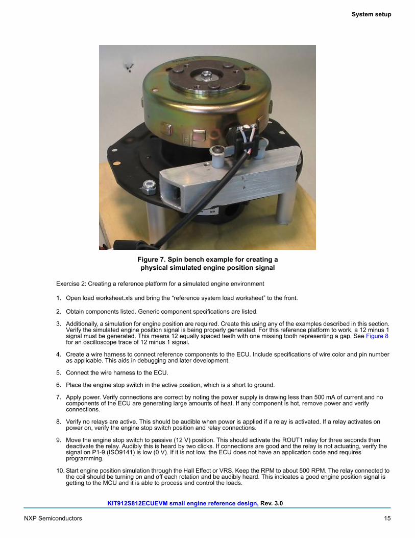
While the concept of a virtual simulated engine position signal is very attractive, it lacks fundamental characteristics coming with an actual crankshaft of an engine. Since a virtual signal is typically generated by a digital computer, it usually does not account for the real world imperfections of an engine. Specifically, the timing pulses produced by a virtual signal are perfect. While this is a good on paper or visually on a screen, the imperfections in the motion due to production tolerance and jerk associated with cylinder compression lead to a less than perfect rotation pattern. As a step in the right direction, a physical simulated engine position signal can be used. This type of setup can take advantage of VRS or Hall Effect sensors and produce a signal having the characteristics of a real engine. A simple and effective way to make a physical simulation is to mount an engine flywheel containing the position teeth to a small electric motor. This creates a tool known as a spin bench. Using an electric motor and the actual flywheel allows simple control of the engine speed while adding real world conditions for changes in the actual time between position teeth. While the strong variations related to compression and combustion are not present, the spin bench does allow transitions to and from a stopped engine and provide teeth representative of the actual engine for which the application is being developed. Figure 7 shows an example of a spin bench using a production flywheel and VRS from a small motorbike.
KIT912S812ECUEVM small engine reference design, Rev. 3.0
NXP Semiconductors 15
System setup
Figure 7. Spin bench example for creating a physical simulated engine position signal
Exercise 2: Creating a reference platform for a simulated engine environment
1. Open load worksheet.xls and bring the “reference system load worksheet” to the front.
2. Obtain components listed. Generic component specifications are listed.
3. Additionally, a simulation for engine position are required. Create this using any of the examples described in this section. Verify the simulated engine position signal is being properly generated. For this reference platform to work, a 12 minus 1 signal must be generated. This means 12 equally spaced teeth with one missing tooth representing a gap. See Figure 8 for an oscilloscope trace of 12 minus 1 signal.
4. Create a wire harness to connect reference components to the ECU. Include specifications of wire color and pin number as applicable. This aids in debugging and later development.
5. Connect the wire harness to the ECU.
6. Place the engine stop switch in the active position, which is a short to ground.
7. Apply power. Verify connections are correct by noting the power supply is drawing less than 500 mA of current and no components of the ECU are generating large amounts of heat. If any component is hot, remove power and verify connections.
8. Verify no relays are active. This should be audible when power is applied if a relay is activated. If a relay activates on power on, verify the engine stop switch position and relay connections.
9. Move the engine stop switch to passive (12 V) position. This should activate the ROUT1 relay for three seconds then deactivate the relay. Audibly this is heard by two clicks. If connections are good and the relay is not actuating, verify the signal on P1-9 (ISO9141) is low (0 V). If it is not low, the ECU does not have an application code and requires programming.
10. Start engine position simulation through the Hall Effect or VRS. Keep the RPM to about 500 RPM. The relay connected to the coil should be turning on and off each rotation and be audibly heard. This indicates a good engine position signal is getting to the MCU and it is able to process and control the loads.

Missing ToothVRS Tooth Signal
(12 minus 1)
Missing ToothHall Effect Tooth
Signal (12 minus 1)
KIT912S812ECUEVM small engine reference design, Rev. 3.0
16 NXP Semiconductors
System setup
Figure 8. Graphical representation of 12 minus 1 tooth pattern on the oscilloscope
7.3 Installation and verification of software development environment
All application software for the ECU is developed using the NXP CodeWarrior for S12X integrated development environment (IDE). The documentation CD, part of the KIT912S812ECUEVM package, includes the latest version of CodeWarrior available at the time of production. To install the program, save then launch the installation application from a temporary location on a Windows based PC or directly launch the installation application. No specific instructions are recommended beyond the default settings shown in the on screen menus. If other versions of the CodeWarrior product are on the PC, this does not overwrite any information as each version is a separate product and installation. For step by step confirmation of the installation process and a quick tutorial on getting started, refer to the CodeWarrior quickstart guide included on the documentation CD. Further information relative to CodeWarrior can be found at www.nxp.com/training. This link has a search feature allowing refinement of high level training topics. One training topic aid in the use of this kit is Learning Programming with C, which can be accessed at the following URL:
http://www.nxp.com/webapp/sps/site/training_information.jsp?code=TP_C_PROGRAMMING&fsrch=1
Additional resources for working with CodeWarrior include the various user manuals installed with CodeWarrior.
Once the CodeWarrior application is installed, the software development environment can be validated.
Software development environment validation exercise
1. Create a new project in CodeWarrior for the MC9S12XS128 MCU using the project wizard appearing when CodeWarrior is launched. Create the project using default settings but be sure to include the USB BDM tool included with your kit as the target connection.
2. Once you have the project created, verify the integrity of the empty software project by doing a build.
3. Once successful, connect the ECU to your 12 V power source using your simulated load harness.
4. Next, connect the PC to the USB BDM tool. Installation will be required if this is the first connection to the PC, follow on screen menu and install driver automatically.
KIT912S812ECUEVM small engine reference design, Rev. 3.0
NXP Semiconductors 17
System setup
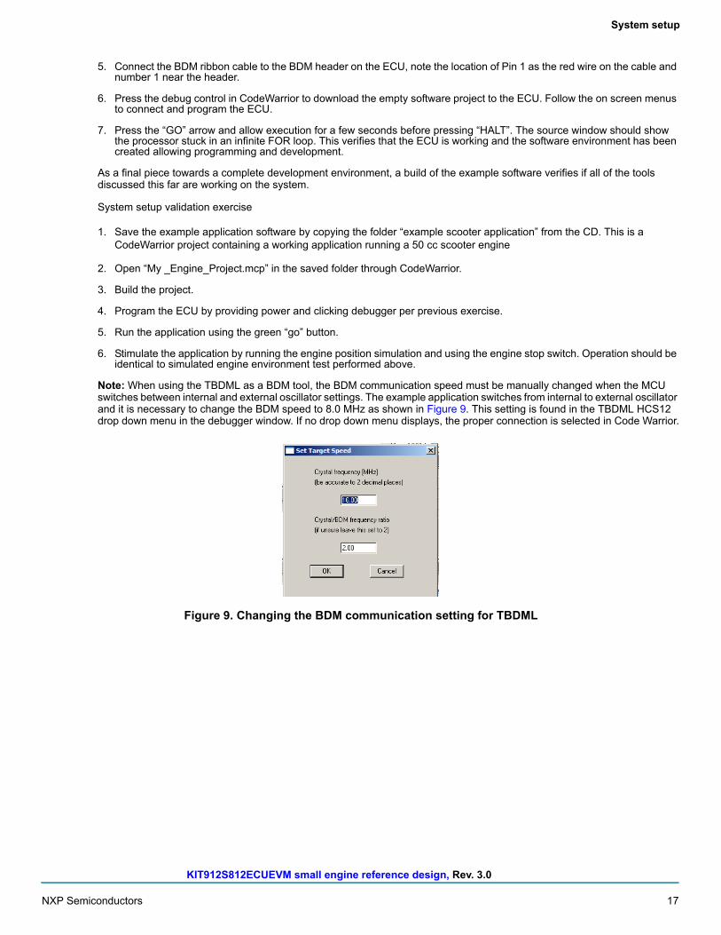
5. Connect the BDM ribbon cable to the BDM header on the ECU, note the location of Pin 1 as the red wire on the cable and number 1 near the header.
6. Press the debug control in CodeWarrior to download the empty software project to the ECU. Follow the on screen menus to connect and program the ECU.
7. Press the “GO” arrow and allow execution for a few seconds before pressing “HALT”. The source window should show the processor stuck in an infinite FOR loop. This verifies that the ECU is working and the software environment has been created allowing programming and development.
As a final piece towards a complete development environment, a build of the example software verifies if all of the tools discussed this far are working on the system.
System setup validation exercise
1. Save the example application software by copying the folder “example scooter application” from the CD. This is a CodeWarrior project containing a working application running a 50 cc scooter engine
2. Open “My _Engine_Project.mcp” in the saved folder through CodeWarrior.
3. Build the project.
4. Program the ECU by providing power and clicking debugger per previous exercise.
5. Run the application using the green “go” button.
6. Stimulate the application by running the engine position simulation and using the engine stop switch. Operation should be identical to simulated engine environment test performed above.
Note: When using the TBDML as a BDM tool, the BDM communication speed must be manually changed when the MCU switches between internal and external oscillator settings. The example application switches from internal to external oscillator and it is necessary to change the BDM speed to 8.0 MHz as shown in Figure 9. This setting is found in the TBDML HCS12 drop down menu in the debugger window. If no drop down menu displays, the proper connection is selected in Code Warrior.
Figure 9. Changing the BDM communication setting for TBDML
KIT912S812ECUEVM small engine reference design, Rev. 3.0
18 NXP Semiconductors
System setup
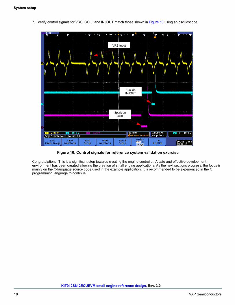
7. Verify control signals for VRS, COIL, and INJOUT match those shown in Figure 10 using an oscilloscope.
VRS Input
Fuel onINJOUT
Spark onCOIL
Figure 10. Control signals for reference system validation exercise
Congratulations! This is a significant step towards creating the engine controller. A safe and effective development environment has been created allowing the creation of small engine applications. As the next sections progress, the focus is mainly on the C-language source code used in the example application. It is recommended to be experienced in the C programming language to continue.

KIT912S812ECUEVM small engine reference design, Rev. 3.0
NXP Semiconductors 19
Application development
8 Application development
There are three paths which can be taken using the small engine reference design for application development: 1) Ground up custom code can be written. 2) The example applications can be modified. 3) A ground up application can be written using the low level drivers and operating system used in the example applications. If a ground up software project is selected, it may be beneficial to use various aspects of the example application for working with the S12 MCU and the other various components in the design. The example application also benefits when using the low level drivers as it serves as an example for using these pieces of code. At the very least, customizing of the example application is required. This section focuses on customizing the example application to a specific engine.
8.1 Example application architecture overview
The example application is designed to run a one or two cylinder engine using a hybrid operating system. A hybrid operating system is important to engine control, as all engine control events are based on the rotation (angle domain) of the engine and user control processing, and the data collection must be performed periodically (time domain). Additionally, the example application reduces complexity through a hardware abstraction layer (HAL). Through the HAL, software complexity is reduced by using application level signal names instead of native control names for the MCU. The combination of these two software techniques produce an example configurable through a single header file and reduces user implemented code to three main functions.
User functions are split into three main activities. In data_management(), all data is collected and processed in the system. This includes analog and digital information and any filter functions to be performed. engine_management() is called to calculate raw fuel and spark parameters for running the engine. This includes a table look up of hard data values based on current engine RPM and load, as well as factoring in fuel and spark modifiers. In User_management(), the engine control strategy is run. It includes interpretations of user control inputs and control strategies for loads. The primary goal of the User management function is to handle user controls, determine fuel modifiers, and calculate engine load. Each of these functions are performed at various rates and configured through the application definitions.h header file. These functions do not directly control the engine fuel and spark events. These are performed by low level functions reacting to the rotation of the engine through the engine position data. The low level engine control events use the latest parameters passed to fuel and spark controllers by the user functions. Additional information is provided in software reference manual found in Section 15, Appendix B: software reference manual, page 54.
8.2 Configuring the application
The first step in working with the example software is to configure the code to be generated through the application definitions.h file. In this file are definitions used to conditionally compile code based on the user defined system. This is done to create an application only using the memory required for the specific application, demonstrate flexible software design through conditional compiling, and create a framework for a custom implementation using various types of hardware. The file is designed to be simple and allow decisions to which definitions to select by using the completed load worksheet, discussed earlier, and knowledge of the application.
While the software provides a signal abstraction layer, configuration of the low level software must be performed through an application header file, “application definitions.h”. This file defines what signals are used in system and provides parameters leading to conditionally compiled code. An example of configuring the software is provided in the demo application. The header file gives a detailed description on how to choose what options desired in the system. Configuring the system through the application header file is done by modifying system parameters by adding or removing specific lines through the comment directive of the C programming language. The following examples goes through various definitions found in the application header file and show possibilities for configuration. It is important to keep in mind the limitations of the hardware as the software incorporates functionality beyond what is found on the reference design hardware.
Example: Configuring the number of cylinders.
//How many cylinders? Choose one.#define ONE_CYLINDER//#define TWO_CYLINDER
To change this application from one cylinder to two cylinders, modify the lines as follows:
//How many cylinders? Choose one.//#define ONE_CYLINDER#define TWO_CYLINDER

KIT912S812ECUEVM small engine reference design, Rev. 3.0
20 NXP Semiconductors
Application development
Other configurations of the application header file require modifying parameters which are numerical in nature. Each value must be customized to the application. Default values are provided but may not be relevant.
Example: Configuring maximum RPM of engine.
//Set the maximum RPM for engine rotation#define RPM_MAX 10000
This parameter can be modified to reduce the maximum RPM from 10 kRPM to 500 RPM as follows:
//Set the maximum RPM for engine rotation#define RPM_MAX 500
For system signals which are configurable, multiple definitions are required. Only if the signal is used do any of the associated parameters, do they need to be defined.
Example: Removing definition of an analog signal.
//Oxygen Sensor(O2)//Define the signal for the system to enable functionality.#define O2//Define for O2 filter algorithm selection. Only average is//available.//Leave undefined for using raw data only. #define AVERAGE_FILTER_O2//Data collection periodic rate can be from 1.0 to 255 ms.#define O2_DATA_COLECTION_RATE 16/* O2 data buffer size */ #define O2_BUFFER_SIZE 16
In this example, if the oxygen sensor is not used, all pound defines should be changed to comments as follows:
//Oxygen Sensor(O2)//Define the signal for the system to enable functionality.//#define O2//Define for O2 filter algorithm selection. Only average is//available.//Leave undefined for using raw data only. //#define AVERAGE_FILTER_O2//Data collection periodic rate can be from 1.0 to 255 ms.//#define O2_DATA_COLECTION_RATE 16/* O2 data buffer size *///#define O2_BUFFER_SIZE 16
One additional configuration is provided outside the application definitions.h file. This is the configuration of the time domain scheduler of the operating system. Configuration of the timing for the tasks is done in the tasks.h file. As seen in Figure 11, the various tasks are configured by placing function calls in the desired task time. While this is an easy way to implement a variety of time based tasks, this simple scheduler does not guarantee task execution time. It is recommended to perform timing analysis using simulation and instrumented software as a part of the application development process.

KIT912S812ECUEVM small engine reference design, Rev. 3.0
NXP Semiconductors 21
Application development
Figure 11. Definition of tasks in tasks.h file
To configure the task timing, edit the definitions shown in Figure 11 using the exact syntax found in the file.
Example: Modifying task times
In this example, the default task scheduler found in the example application is modified to show how to slow down the execution of user_management() and add a custom function to be run every 1.0 ms called Heartbeat().
1. Open the example application using CodeWarrior.
2. Open the file “tasks.h”.
3. Find the definition section containing the 10 ms tasks.
4. Select the line containing the function call “user_management()”. Cut this line from the code.
5. Place the user management task by copying it into the space for 100 ms tasks.
6. In the 1.0 ms task section, add a line containing the function call “Heartbeat()” and follow syntax shown for other tasks
When complete the code shown in Figure 11 should look exactly like the code shown in Figure 12.

KIT912S812ECUEVM small engine reference design, Rev. 3.0
22 NXP Semiconductors
Application development
Figure 12. Modifications of tasks.h from example exercise
8.2.1 Fuel and spark data tables
As a means to input data used for fuel and spark values, an application map tool based on a spreadsheet is provided. This tool provides the essential functionality for translating fuel and spark data tables into content which can be placed into the example software. Specific engine management data can be placed into the tool using engineering units. This table is then converted to microcontroller units in a C-source friendly format. Map table sizes can be adjusted to meet application requirements. The application map tool is identified as “map tool.xls”. Additionally, reference for an example map is provided in “scooter map.xls”. This provides an example of a completed map as used in the example application.
8.2.2 Modifying table sizes
As a first step, the table size should be customized to accommodate the performance and data requirements. This is accomplished by adjusting the number of load points and RPM points in the table. In the empty map provided (map tool.xls), this is done by changing number of and content of the load row (green) and the RPM column (yellow) values. Both the number of load and RPM values directly impact the size of the table and speed at which the table look up is performed.
While more data points gives you better tuning ability, it increases the size of the application and increases the worst case time to perform the table look up. Another factor used for sizing the tables is available data. If a legacy map is used, then the simplest starting point is to directly reuse this map. If a new map is to be created by empirical data through testing, a smaller map is the best starting point.
KIT912S812ECUEVM small engine reference design, Rev. 3.0
NXP Semiconductors 23
Application development
Fuel and spark maps are independent of each other and the load and RPM points must be customized for both sets of data. Using the “fuel engineering units (ms)” and the “spark engineering units (BTDC)” worksheets, enter the desired number of points and values for each point for the load row and RPM column. Load is input as a percentage from 0% to 100% in ascending order, left to right. RPM is input from 0 to your max RPM in ascending order, top to bottom.
When determining the max RPM, consider the performance of the engine as well as the resolution of the software. For the example application software, a fundamental timing unit is 1.6 μs. This means the highest resolution between RPM measurements is 1.6 μs. However, RPM, or engine speed, is determined from the tooth period measurements on the engine's flywheel. This means while the engine is rotating at a given RPM, the measurement taken is at a fraction of this rate.
For example, at 6000 RPM, an engine completes one rotation every 10 ms. The engine controller monitors position of the engine through the teeth on the flywheel. Each engine has a specific number of teeth. For this example the engine has 12 teeth. The result is, the engine controller measures the time between two teeth at 6000 RPM as 833 μs. Looking at the fundamental timing unit, the software provides a measurement of 520 (really 520.8 but quantization results in 520).
At 6000 RPM, there is not much sensitivity due to the 1.6 μs timing unit as there is a count of 520. However, as the RPM and number of teeth increases so does the sensitivity. This concept is important to understand and also is relevant for low RPM conditions as well. At low RPM, the maximum time which can be measured is 104.5 ms. For the 12 tooth engine example, this corresponds to 47 RPM.
8.2.3 Configuring data translation
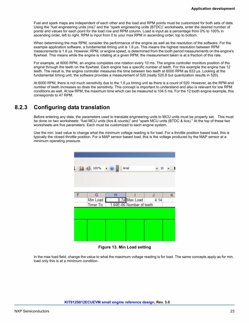
Before entering any data, the parameters used to translate engineering units to MCU units must be properly set. This must be done on two worksheets: “fuel MCU units (tics & counts)” and “spark MCU units (BTDC & tics).” At the top of these two worksheets are five parameters. Each must be customized to each engine system.
Use the min. load value to change what the minimum voltage reading is for load. For a throttle position based load, this is typically the closed throttle position. For a MAP sensor based load, this is the voltage produced by the MAP sensor at a minimum operating pressure.
Figure 13. Min Load setting
In the max load field, change the value to what the maximum voltage reading is for load. The same concepts apply as for min. load only this is at a minimum condition.

KIT912S812ECUEVM small engine reference design, Rev. 3.0
24 NXP Semiconductors
Application development
Figure 14. Max Load setting
For the ADC ref field, input the reference voltage for the analog measurement. The small engine reference design uses 5.0 V as the reference and this should not be changed.
Figure 15. ADC Ref voltage setting
Depending on the software configuration, analog data is collected as 8, 10, or 12 bits. Make sure this field matches how the software is configured.

KIT912S812ECUEVM small engine reference design, Rev. 3.0
NXP Semiconductors 25
Application development
Figure 16. ADC bits setting
The final field to be completed is the number of teeth. This is the number of teeth on the flywheel as used for synchronization and engine speed measurement. Use the total number of teeth including missing teeth as the spacing is the important characteristic. For example, an engine may have a 12 minus one tooth configuration, meaning 12 equally spaced teeth and one of the teeth is removed for synchronization. In this case the relevant number is 12.
Figure 17. Number of teeth setting
8.2.4 Entering map data
Each combination of load and RPM value creates a unique data point which can be accessed by the software during execution. The data for fuel and spark maps are input into the “fuel engineering units (ms)” and the “spark engineering units (BTDC)” input worksheets, respectively. As data is entered in these two worksheets, it is translated on the “fuel MCU units (tics & counts)” and the “spark MCU units (BTDC & tics)” output worksheets. These two output worksheets contain the same data as the input worksheets only translated based on the MCU and software configuration.
KIT912S812ECUEVM small engine reference design, Rev. 3.0
26 NXP Semiconductors
Application development
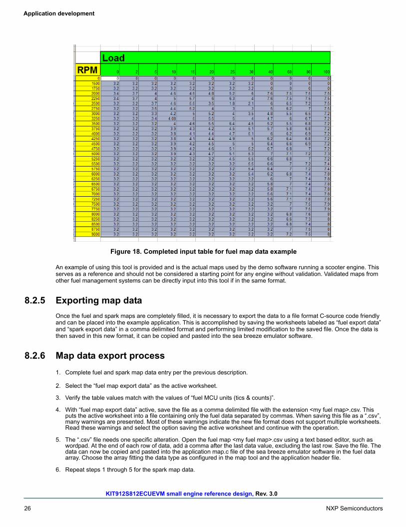
Figure 18. Completed input table for fuel map data example
An example of using this tool is provided and is the actual maps used by the demo software running a scooter engine. This serves as a reference and should not be considered a starting point for any engine without validation. Validated maps from other fuel management systems can be directly input into this tool if in the same format.
8.2.5 Exporting map data
Once the fuel and spark maps are completely filled, it is necessary to export the data to a file format C-source code friendly and can be placed into the example application. This is accomplished by saving the worksheets labeled as “fuel export data” and “spark export data” in a comma delimited format and performing limited modification to the saved file. Once the data is then saved in this new format, it can be copied and pasted into the sea breeze emulator software.
8.2.6 Map data export process
1. Complete fuel and spark map data entry per the previous description.
2. Select the “fuel map export data” as the active worksheet.
3. Verify the table values match with the values of “fuel MCU units (tics & counts)”.
4. With “fuel map export data” active, save the file as a comma delimited file with the extension <my fuel map>.csv. This puts the active worksheet into a file containing only the fuel data separated by commas. When saving this file as a “.csv”, many warnings are presented. Most of these warnings indicate the new file format does not support multiple worksheets. Read these warnings and select the option saving the active worksheet and continue with the operation.
5. The “.csv” file needs one specific alteration. Open the fuel map <my fuel map>.csv using a text based editor, such as wordpad. At the end of each row of data, add a comma after the last data value, excluding the last row. Save the file. The data can now be copied and pasted into the application map.c file of the sea breeze emulator software in the fuel data array. Choose the array fitting the data type as configured in the map tool and the application header file.
6. Repeat steps 1 through 5 for the spark map data.
KIT912S812ECUEVM small engine reference design, Rev. 3.0
NXP Semiconductors 27
Application development
Additionally, information regarding the size of the table and the actual values of for each of the load and RPM values must be put into the application map.c file. The same process used for the table data can be used for the load and RPM values using specific export tabs and previous procedure provided. The number of load and RPM points for the fuel and spark arrays must be put into the application map.h file. It is up to the user to ensure the table is sized properly for the data input into the actual map. Errors in the size of the data tables or the data used for each load or RPM value result in an improper table look up procedure, which may result in random data used to create fuel and spark events. Use the demo application as a guide if there is doubt in the procedure.
8.2.7 Working with the example application
The demo application is based on a simple application state machine (ASM) for engine control. This state machine executes in the user_management() task and can be found in the user_management.c file. A combination of user controls and engine operating parameters are used to control the states of the application. The five states of the ASM are: INIT, STOP, START, RUN, and OVERRUN. A function call is provided for transitioning to each state. This allows a more controlled engine operating mode when changing states.
Description of user management states
INIT
This state provides a known configuration of the user management task and should be configured as the initial state using user_management_init(). Variables for user management should be initialized and any essential activity necessary to be performed prior to operating in any other state should be done in the INIT state. Once this activity completes, the ASM should transition to the STOP state where the periodic activity begins. Optionally, if a major system error occurred, the user may find it necessary to return to this state.
STOP
In this state, the engine decided to be stopped from rotating or running. System inputs such as switches would typically cause the application to enter the STOP state. The application should configure any outputs or controllers to match this request to stop the engine and remain in this state until the inputs reflect going to an active engine state.
START
As a provision for a slowly rotating engine or in preparation for the engine to begin rotating, the START state allows the application to initialize engine controls for an active mode. This state is maintained as long as the engine stays below a minimum speed, identified in the user management header file as the stall speed. Additionally, the same system inputs allowing the exit of the STOP state must be present or a transition to the STOP state would occur.
RUN
Once a minimum engine speed has been obtained and the correct system inputs have been applied, the RUN state represents the normal operating state of the application for a rotating or running engine. The engine control strategy is to be implemented in this state. System inputs must be maintained to keep the engine in the RUN state and the engine speed must be above the stall speed but below the maximum speed, identified in the user’s management header file as over speed.
OVERRUN
As a special case for an active engine, the OVERRUN state provides a way to limit the engine speed. This can be implemented by changing the engine control outputs through variables or through disabling specific engine control outputs. System inputs for an active engine state must be maintained to prevent the ASM from going to the STOP state.
Additionally the engine speed must be reduced below a specific value. This parameter is adjusted in the user management header file as over speed recovery.
The true performance of the small engine reference design can only be shown in a real application. Through development using a real engine, testing can be performed addressing real system issues with an engine control application. Using a real production scooter as a test platform demonstrates the capabilities of the hardware and software beyond documentation. For this purpose, a demonstration application using the 50 cc EFI motorbike was selected. By retrofitting the engine controller with the small engine reference design, a basic engine management application is demonstrated.
KIT912S812ECUEVM small engine reference design, Rev. 3.0
28 NXP Semiconductors
System overview
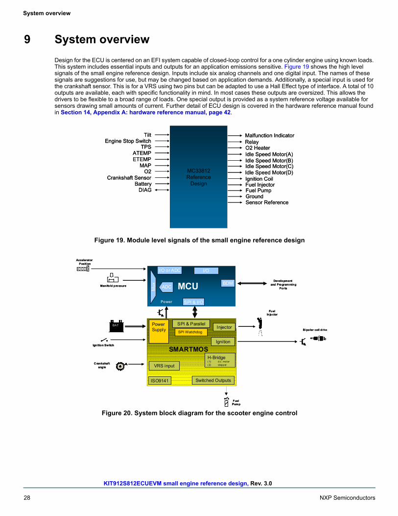
9 System overview
Design for the ECU is centered on an EFI system capable of closed-loop control for a one cylinder engine using known loads. This system includes essential inputs and outputs for an application emissions sensitive. Figure 19 shows the high level signals of the small engine reference design. Inputs include six analog channels and one digital input. The names of these signals are suggestions for use, but may be changed based on application demands. Additionally, a special input is used for the crankshaft sensor. This is for a VRS using two pins but can be adapted to use a Hall Effect type of interface. A total of 10 outputs are available, each with specific functionality in mind. In most cases these outputs are oversized. This allows the drivers to be flexible to a broad range of loads. One special output is provided as a system reference voltage available for sensors drawing small amounts of current. Further detail of ECU design is covered in the hardware reference manual found in Section 14, Appendix A: hardware reference manual, page 42.
MC33812Reference
Design
TiltEngine Stop Switch
TPSATEMPETEMP
MAPO2
Crankshaft SensorBattery
DIAG
Malfunction IndicatorRelayO2 HeaterIdle Speed Motor(A)Idle Speed Motor(B)Idle Speed Motor(C)Idle Speed Motor(D)Ignition CoilFuel InjectorFuel PumpGroundSensor Reference
MC33812Reference
Design
TiltEngine Stop Switch
TPSATEMPETEMP
MAPO2
Crankshaft SensorBattery
DIAG
Malfunction IndicatorRelayO2 HeaterIdle Speed Motor(A)Idle Speed Motor(B)Idle Speed Motor(C)Idle Speed Motor(D)Ignition CoilFuel InjectorFuel PumpGroundSensor Reference
Figure 19. Module level signals of the small engine reference design
MCU
AcceleratorPosition
BDMDevelopment
and ProgrammingPorts
Power
Ignition Switch
SPI & I/O
Power Supply
SMARTMOS
VRS input
ISO9141
H-Bridge( 1) d.c . motor( 2) stepper
Switched Outputs
InjectorSPI & Parallel
Ignition
BAT
ADC
Crankshaftangle
Mux
SPI Watchdog
I/O or ADC
Bipolar coil drive
I/O
Fuel Inje ctor
Manifold pre ssure
FuelPump
MCU
AcceleratorPosition
BDMDevelopment
and ProgrammingPorts
Power
Ignition Switch
SPI & I/O
Power Supply
SMARTMOS
VRS input
ISO9141
H-Bridge( 1) d.c . motor( 2) stepper
Switched Outputs
InjectorSPI & Parallel
Ignition
BATBAT
ADC
Crankshaftangle
Mux
SPI Watchdog
I/O or ADC
Bipolar coil drive
I/O
Fuel Inje ctor
Manifold pre ssure
FuelPump
Figure 20. System block diagram for the scooter engine control

KIT912S812ECUEVM small engine reference design, Rev. 3.0
NXP Semiconductors 29
Application overview
10 Application overview
The scooter demo application uses the same simple state machine that described above. Complexity of the application is limited to an Alpha N engine management strategy with system modifier parameters. Engine management strategy uses table look up for fuel and spark parameters based on throttle position and engine speed. Although table look up is restricted to exact values on the table, interpolation between points is can be easily implemented through custom code. Once the table look up value has been obtained for fuel and spark, various modifier values can used to obtain the final value used by the fuel and spark controllers.
These fuel and spark modifiers are determined and managed by the user management task. The example application only uses two modifiers in the application, but provides the framework for an advanced algorithm. These variables are maintained in the user management task but are added to the table look up base value in a low level function. This action is performed in u16calc_fuel_pulse_width(), which is used by the engine management task. Additionally, two fuel variables are available for tuning to directly control the fuel pulse output when a fuel event is scheduled. These two variables are fuel_cut and fuel_add and have companion variables for spark, referenced as spark_advance and spark_retard. These direct fuel and spark modifiers are extremely useful for coarse and fine tuning of the engine without the complexity of multiple modifiers.
For starting conditions, a fuel modifier value, FM_MSTART, adds additional fuel to the base look up table value. When in the START state, a calibration value of MSTART is used. When the engine speed increases to the RUN state, the FM_MSTART fuel modifier is decayed at a specific rate, MSTART_Decay_Timeout, based on execution of the User Management task. The amount of the decay is set by MSTART_Decay. Both values are sent in the User Management header file. This working example shows how others can be used in a more advanced implementation.
For transient operation, the fuel modifier FM_MACCEL is used. Parameters associated with the transient fuel detection are found in the user management header file. Tip in and tip out can be detected and individually handled. Thresholds based on ADC count changes between new TPS_Filtered data values can be configured along with decay size and rates. Transient fuel operation is intended to emulate the accelerator pump functionality of a carburetor.
This application also demonstrates active load control through time-outs. The example used is the fuel pump. When the application state machine is in the STOP state, the application must be ready to begin starting the engine at anytime. As a strategy, pressurizing the fuel system is best done before any attempt to fuel the engine is made. As a result, the fuel pump is turned on in the STOP state. However, if the fuel pump was left on unconditionally, the battery would be discharged quickly. To prevent this, a timeout is used so the fuel pump is turned off after three seconds in the STOP state. This parameter is defined in the user management header file as FUEL_PUMP_TIMEOUT and the fuel pump activity is controlled by the fuel_pump_controller(). This simple routine is provided to show how time based management of the loads can be done using engine operating states.
For a four-stroke engine, the process is a 720 degree cycle. Additional synchronization techniques must be performed to transfer the low level processes from a two-stroke to a four-stroke operating mode. For a one cylinder engine, a simple technique can be done to eliminate the need of an additional camshaft sensor. If the system uses manifold absolute pressure (MAP), measurements can be performed to determine if the engine is in a compression or exhaust stroke. This requires looking for a specific signature of the MAP signal. This must be done at the low level. To do this, a toothed based MAP data collection process is selected in the application header file. Specific teeth for collecting data are defined. Signature detection is implemented in the crank_state_ISR() in the SYNCHRONIZED state in crank_sensing.c file. This signature detection algorithm can be easily customized. Implementation using a cam sensor is also easily accommodated for as a simple flag enables the transition from the two-stroke mode to four-stroke mode.
In the application state machine, clear areas are defined to implement engine strategy. A simple example is provided based on using an Alpha N engine control strategy. The software is not intended to show an optimized strategy, however it is designed to provide a starting point for development of an engine management application which is modular and can be successful in running an engine. Thorough understanding and optimization are required when applying this software to any engine application.
Updating low level code
There are no committed support plans for the example application software. It is recommended to continue the customizing of the software down to the lowest level if it is to be used beyond a demonstration purpose. This would include correction of errors for compilations and operation as well as application hardening of software both at the application level and microcontroller level. In event of a significant low level driver update or third party software addition, low level code can be updated in two different ways.
Method 1: Using the new software project containing the new low level driver code, copy in the contents of the user functions. These include user_management(), engine_management(), data_management(), and application map data. Include any custom definitions in the header files as well.

KIT912S812ECUEVM small engine reference design, Rev. 3.0
30 NXP Semiconductors
Application overview
Method 2: Import new driver files on an individual basis. For specific file updates, copy and overwrite the specific file and header file of interest into the project directory folder structure. Be sure to do a clean build by removing all object code as well as back up the project before overwriting files. Additional dependencies may need to be considered as new code could make use of other new code not found in the replaced file.
10.1 Application testing
Before going to a real system with your application, extensive testing is recommended to ensure any engine control signals, specifically fuel and spark, meet the timing requirements, and the application provides the desired high level operation and user control. This is best achieved with the simulated system set up previously. Once the application is validated at the bench level, it may be necessary to reduce system functionality and test basic operation when migrating to real engine hardware. Data collection, load control, and system start/stop conditions can be easily tested without the engine running. Additional testing can be performed with fuel and spark controls physically disabled which provides an opportunity for analysis of the rotating engine with no combustion events. Control signals for fuel and spark can then be verified using the actual loads in preparation for calibration of engine control parameters.
Testing the application can be done in real-time using the debugger built into the CodeWarrior IDE. This tool allows non-intrusive debugging through the microcontroller’s BDM pin while the processor is running. Using the debugger allows setting breakpoints, step though code, view, and modify software variables, and directly control the registers of the S12X microcontroller. Through the use of calibration variables able to be modified using the debugger, testing can be performed to find working values for system control parameters.
One of the most difficult aspects to master is the angle based operation of the engine. It may take many iterations of software building and testing to get the timing right for the delivery of the fuel and spark pulses. Some of this confusion may come from the generic implementation of the example application. The crankshaft state machine that synchronizes to the rotation of the engine, through the teeth pulses on the crankshaft, uses the missing tooth as the definition of top dead center or 0 degrees. The first tooth after the missing tooth gap is then tooth 1. This is not always the case and an offset needs to be created to compensate for specific engine implementation. In the example application, the missing tooth gap is actually at bottom dead center. This creates an offset of 6 teeth (12 minus 1 wheel defined) that must be accounted for. The end result in this case is the top dead center must be defined as tooth 7, creating an offset of 180 degrees.
Once this is compensated for in the application, adjustment of the timing for fuel and spark is handled by the application maps. It may be necessary to create a test map for fuel and spark to verify timing is being properly controlled. Small test maps help provide useful validation tools. Test maps with all the same data are good for basic timing validation. Progressive value maps provide a way to validated table look up is performed as expected.
In the example application, one of the most important calibration variables is the MSTART. This is a fuel modifier variable adding additional time to the fuel pulse when the application is in the START state. Proper setting of this variable depends on the engine and fuel injector used, as well as atmospheric conditions. With the debugger open and the application running, it is possible to adjust the MSTART value between starting attempts to adjust the amount of extra fuel is added during startup. This is a delicate process and leads to the art of engine calibration. As calibration is performed, it is important to get back to a steady state before testing a new value. Specifically for MSTART, it is difficult as the failure to start and run the engine can leave the engine cylinder with raw fuel and easily foul the spark plug.
As development of your application progresses, it needs to incorporate features for performance and safety. It is advised to balance hard testing with simulation exercises. This is a necessary step in the development process accounting for worst case code execution. Independent exercises for RAM utilization and execution timing should be considered so bandwidth of the system is not at 100%, which can easily result in poor engine operation or runaway code due to stack overflow. This leaves room for addition unforeseen complexity which can only come from code execution on the real system.

MM
912J
P8
12A
MA
F
SiP
= S
12P
128
& M
C3
3812
KIT912S812ECUEVM small engine reference design, Rev. 3.0
NXP Semiconductors 31
Schematic
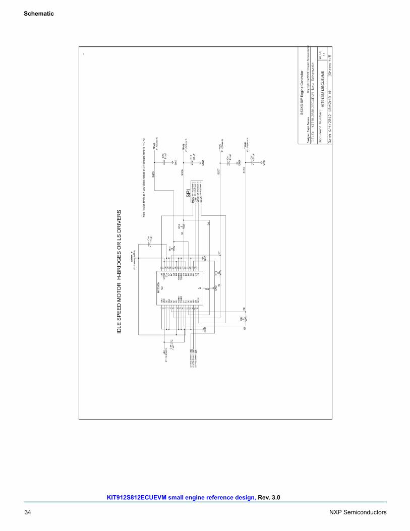
11 Schematic

KIT912S812ECUEVM small engine reference design, Rev. 3.0
32 NXP Semiconductors
Schematic

KIT912S812ECUEVM small engine reference design, Rev. 3.0
NXP Semiconductors 33
Schematic
KIT912S812ECUEVM small engine reference design, Rev. 3.0
34 NXP Semiconductors
Schematic

KIT912S812ECUEVM small engine reference design, Rev. 3.0
NXP Semiconductors 35
Board layout
12 Board layout
12.1 Assembly layer top

KIT912S812ECUEVM small engine reference design, Rev. 3.0
36 NXP Semiconductors
Board layout
12.2 Assembly layer bottom

KIT912S812ECUEVM small engine reference design, Rev. 3.0
NXP Semiconductors 37
Board layout
12.3 Top layer routing

KIT912S812ECUEVM small engine reference design, Rev. 3.0
38 NXP Semiconductors
Board layout
12.4 Bottom layer routing
KIT912S812ECUEVM small engine reference design, Rev. 3.0
NXP Semiconductors 39
Bill of materials
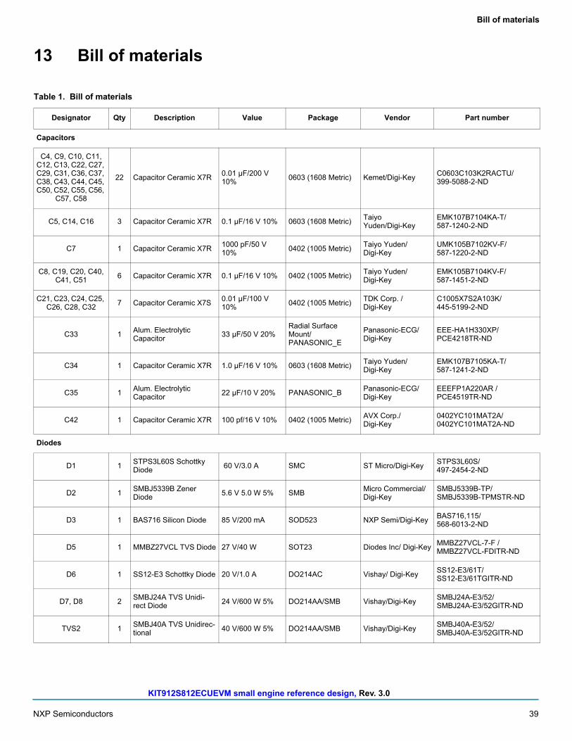
13 Bill of materials
Table 1. Bill of materials
Designator Qty Description Value Package Vendor Part number
Capacitors
C4, C9, C10, C11, C12, C13, C22, C27, C29, C31, C36, C37, C38, C43, C44, C45, C50, C52, C55, C56,
C57, C58
22 Capacitor Ceramic X7R0.01 μF/200 V 10%
0603 (1608 Metric) Kemet/Digi-KeyC0603C103K2RACTU/ 399-5088-2-ND
C5, C14, C16 3 Capacitor Ceramic X7R 0.1 μF/16 V 10% 0603 (1608 Metric)Taiyo Yuden/Digi-Key
EMK107B7104KA-T/ 587-1240-2-ND
C7 1 Capacitor Ceramic X7R1000 pF/50 V 10%
0402 (1005 Metric)Taiyo Yuden/ Digi-Key
UMK105B7102KV-F/ 587-1220-2-ND
C8, C19, C20, C40, C41, C51
6 Capacitor Ceramic X7R 0.1 μF/16 V 10% 0402 (1005 Metric)Taiyo Yuden/ Digi-Key
EMK105B7104KV-F/ 587-1451-2-ND
C21, C23, C24, C25, C26, C28, C32
7 Capacitor Ceramic X7S0.01 μF/100 V 10%
0402 (1005 Metric)TDK Corp. / Digi-Key
C1005X7S2A103K/ 445-5199-2-ND
C33 1Alum. Electrolytic Capacitor
33 μF/50 V 20%Radial Surface Mount/ PANASONIC_E
Panasonic-ECG/ Digi-Key
EEE-HA1H330XP/ PCE4218TR-ND
C34 1 Capacitor Ceramic X7R 1.0 μF/16 V 10% 0603 (1608 Metric)Taiyo Yuden/ Digi-Key
EMK107B7105KA-T/ 587-1241-2-ND
C35 1Alum. Electrolytic Capacitor
22 μF/10 V 20% PANASONIC_BPanasonic-ECG/ Digi-Key
EEEFP1A220AR / PCE4519TR-ND
C42 1 Capacitor Ceramic X7R 100 pf/16 V 10% 0402 (1005 Metric)AVX Corp./ Digi-Key
0402YC101MAT2A/ 0402YC101MAT2A-ND
Diodes
D1 1STPS3L60S Schottky Diode
60 V/3.0 A SMC ST Micro/Digi-KeySTPS3L60S/ 497-2454-2-ND
D2 1SMBJ5339B Zener Diode
5.6 V 5.0 W 5% SMBMicro Commercial/ Digi-Key
SMBJ5339B-TP/ SMBJ5339B-TPMSTR-ND
D3 1 BAS716 Silicon Diode 85 V/200 mA SOD523 NXP Semi/Digi-KeyBAS716,115/ 568-6013-2-ND
D5 1 MMBZ27VCL TVS Diode 27 V/40 W SOT23 Diodes Inc/ Digi-KeyMMBZ27VCL-7-F / MMBZ27VCL-FDITR-ND
D6 1 SS12-E3 Schottky Diode 20 V/1.0 A DO214AC Vishay/ Digi-KeySS12-E3/61T/ SS12-E3/61TGITR-ND
D7, D8 2SMBJ24A TVS Unidi-rect Diode
24 V/600 W 5% DO214AA/SMB Vishay/Digi-KeySMBJ24A-E3/52/ SMBJ24A-E3/52GITR-ND
TVS2 1SMBJ40A TVS Unidirec-tional
40 V/600 W 5% DO214AA/SMB Vishay/Digi-KeySMBJ40A-E3/52/ SMBJ40A-E3/52GITR-ND

KIT912S812ECUEVM small engine reference design, Rev. 3.0
40 NXP Semiconductors
Bill of materials
Transistors
Q2 1 IRG4RC10KPbF IGBT600 V/9.0 A UFAST
DPAK IR/Digi-KeyIRG4RC10KPbF /IRG4RC10KPBF-ND
Q3, Q4 2 IRF7341 Dual MOSFET 55 V/4.7 A 8-SOIC IR/Digi-Key IRF7341TRPBF/ IRF7341PBFTR-ND
Q5 1FZT789A Replacement PNP Transistor
45 V/1.0 A SOT223Diodes/Zetex /Digi-Key
BCP5116TA/ BCP5116TATR-ND
Resistors
R1, R6, R42, R48, R51, R55, R57, R59
8 Resistor 1/10 Watt 5% 10 kΩ 0402 (1005 Metric)
Panasonic-ECG/ Digi-Key
ERJ-2GEJ103X/ P10KJTR-ND
R2, R3, R16, R28, R32
5 Resistor 1/10 Watt 5% 15 kΩ 0402 (1005 Metric)
Panasonic-ECG/ Digi-Key
ERJ-2GEJ153X/ P15KJTR-ND
R4 1 Resistor 1/10 Watt 5% 1.0 kΩ 0402 (1005 Metric)
Panasonic-ECG/ Digi-Key
ERJ-2GEJ102X/ P1.0KJTR-ND
R5 1 Resistor 1/10 Watt 5% 47 kΩ 0402 (1005 Metric)
Panasonic-ECG/ Digi-Key
ERJ-2GEJ473X/ P47KJTR-ND
R7 1 Resistor 1/10 Watt 1% 3.1 kΩ 0402 (1005 Metric)
Panasonic-ECG/ Digi-Key
ERJ-2RKF3091X/ P3.09KLTR-ND
R10, R11, R12, R13, R15
4 Resistor 1/8 Watt 0 Ω 0805 (2012 Metric)
Panasonic-ECG/ Digi-Key
ERJ-6GEY0R00V/ P0.0ATR-ND
R17, R18, R24, R40, R41
5 Resistor 1/10 Watt 5% 16 kΩ 0402 (1005 Metric)
Panasonic-ECG/ Digi-Key
ERJ-2GEJ163X/ P16KJTR-ND
R22 1 Resistor 1/10 Watt 1% 31.6 kΩ 0402 (1005 Metric)
Panasonic-ECG/ Digi-Key
ERJ-2RKF3162X/ P31.6KLTR-ND
R33, R47, 2 Resistor 1/10 Watt 5% 6.8 kΩ 0402 (1005 Metric)
Panasonic-ECG/ Digi-Key
ERJ-2GEJ682X/ P6.8KJTR-ND
R37 1 Resistor 1 Watt 5% 36 kΩ 2512 (6432 Metric)
Panasonic-ECG/ Digi-Key
ERJ-1TYJ363U/ PT36KXTR-ND
R38 1 Resistor 1/4 Watt 1% 4.02 kΩ 1206 (3216 Metric)
Panasonic-ECG/ Digi-Key
ERJ-8ENF4021V/ P4.02KFTR-ND
R39 1 Resistor 1/10 Watt 1% 4.99 kΩ 0402 (1005 Metric)
Panasonic-ECG/ Digi-Key
ERJ-2RKF4991X/ P4.99KLTR-ND
ICs
U1 1Small Engine Control Analog SiP
LQFP100-EP NXP MM912JS812AMAF
U2 1 Configurable Driver 32-SOIC-EP NXP MC33880PEW
U3 1MAX9924 VRS Input Conditioning IC
UMAX10MAXIM/ Digi-Key
MAX9924UAUB+/ MAX9924UAUB+-ND
XTAL1 1 Ceramic Resonator 8.0 MHz ±0.2% Custom SMTMurata/ Digi-Key
CSTCE8M00G55-R0/ 490-1195-2-ND
Table 1. Bill of materials (continued)
Designator Qty Description Value Package Vendor Part number

KIT912S812ECUEVM small engine reference design, Rev. 3.0
NXP Semiconductors 41
Bill of materials
Connectors and PC board
BDM 1 Header SMT (2x3) 0.100 Pitch MA03-2SM FCI/Digi-Key95278-101A06LF/ 609-3487-2-ND
CAN1 1 Header through hole (2x2) 0.100 Pitch MA2-2SMTE Connectivity/ Digi-Key
87227-2/ A26567-ND
P1 1 Connector 16 Position (2x8) 5566-16Tyco Electronics/ Digi-Key
1-1586039-6/ A30675-ND
P2 1 Connector 12 Position (2x6) 5566-12Tyco Electronics/ Digi-Key
1-1586039-2/ A30673-ND
WD_INH_JMPR 1 Header through hole (2x1) MA02-1Tyco Electronics/ Digi-Key
87220-2/ A26542-ND
Note: NXP does not assume liability, endorse, or warrant components from external manufacturers that are referenced in circuit drawings or tables. While NXP offers component recommendations in this configuration, it is the customer’s responsibility to validate their application.
Table 1. Bill of materials (continued)
Designator Qty Description Value Package Vendor Part number
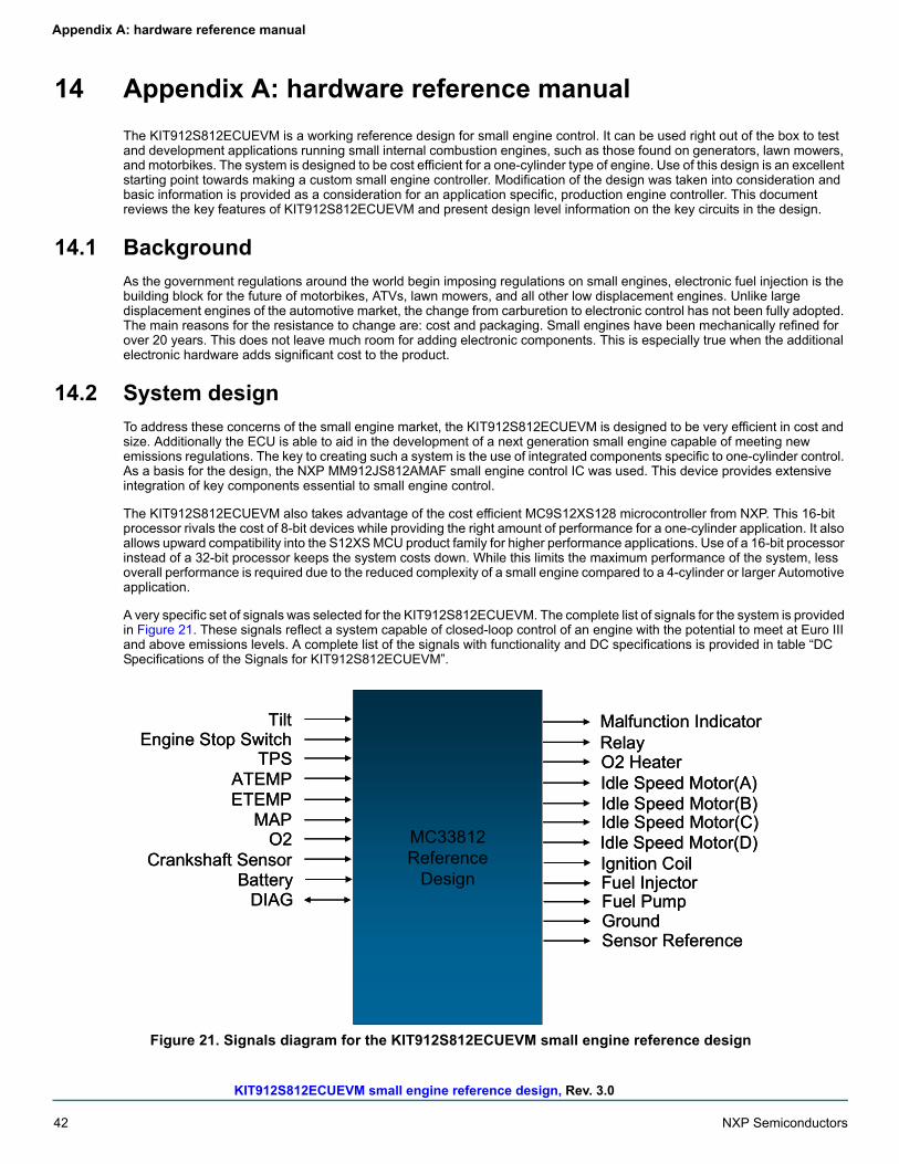
KIT912S812ECUEVM small engine reference design, Rev. 3.0
42 NXP Semiconductors
Appendix A: hardware reference manual
14 Appendix A: hardware reference manual
The KIT912S812ECUEVM is a working reference design for small engine control. It can be used right out of the box to test and development applications running small internal combustion engines, such as those found on generators, lawn mowers, and motorbikes. The system is designed to be cost efficient for a one-cylinder type of engine. Use of this design is an excellent starting point towards making a custom small engine controller. Modification of the design was taken into consideration and basic information is provided as a consideration for an application specific, production engine controller. This document reviews the key features of KIT912S812ECUEVM and present design level information on the key circuits in the design.
14.1 Background
As the government regulations around the world begin imposing regulations on small engines, electronic fuel injection is the building block for the future of motorbikes, ATVs, lawn mowers, and all other low displacement engines. Unlike large displacement engines of the automotive market, the change from carburetion to electronic control has not been fully adopted. The main reasons for the resistance to change are: cost and packaging. Small engines have been mechanically refined for over 20 years. This does not leave much room for adding electronic components. This is especially true when the additional electronic hardware adds significant cost to the product.
14.2 System design
To address these concerns of the small engine market, the KIT912S812ECUEVM is designed to be very efficient in cost and size. Additionally the ECU is able to aid in the development of a next generation small engine capable of meeting new emissions regulations. The key to creating such a system is the use of integrated components specific to one-cylinder control. As a basis for the design, the NXP MM912JS812AMAF small engine control IC was used. This device provides extensive integration of key components essential to small engine control.
The KIT912S812ECUEVM also takes advantage of the cost efficient MC9S12XS128 microcontroller from NXP. This 16-bit processor rivals the cost of 8-bit devices while providing the right amount of performance for a one-cylinder application. It also allows upward compatibility into the S12XS MCU product family for higher performance applications. Use of a 16-bit processor instead of a 32-bit processor keeps the system costs down. While this limits the maximum performance of the system, less overall performance is required due to the reduced complexity of a small engine compared to a 4-cylinder or larger Automotive application.
A very specific set of signals was selected for the KIT912S812ECUEVM. The complete list of signals for the system is provided in Figure 21. These signals reflect a system capable of closed-loop control of an engine with the potential to meet at Euro III and above emissions levels. A complete list of the signals with functionality and DC specifications is provided in table “DC Specifications of the Signals for KIT912S812ECUEVM”.
MC33812Reference
Design
TiltEngine Stop Switch
TPSATEMPETEMP
MAPO2
Crankshaft SensorBattery
DIAG
Malfunction IndicatorRelayO2 HeaterIdle Speed Motor(A)Idle Speed Motor(B)Idle Speed Motor(C)Idle Speed Motor(D)Ignition CoilFuel InjectorFuel PumpGroundSensor Reference
MC33812Reference
Design
TiltEngine Stop Switch
TPSATEMPETEMP
MAPO2
Crankshaft SensorBattery
DIAG
Malfunction IndicatorRelayO2 HeaterIdle Speed Motor(A)Idle Speed Motor(B)Idle Speed Motor(C)Idle Speed Motor(D)Ignition CoilFuel InjectorFuel PumpGroundSensor Reference
Figure 21. Signals diagram for the KIT912S812ECUEVM small engine reference design

KIT912S812ECUEVM small engine reference design, Rev. 3.0
NXP Semiconductors 43
Appendix A: hardware reference manual
.
Table 2. DC specifications of the signals for KIT912S812ECUEVM
Connector PinSignal name
Signal typeVoltage range
Recommended functionality
Connector PinSignal name
Signal typeVoltage range
Recommended functionality
KIT912S812ECUEVM reference design
P1
1 VPWR Power input 14 V System power from 12 V battery
2 COIL Output with feedback 0-14 V Spark control of digital ignition system.
3 GND Power output 0 V Module level ground reference, return path of VBAT
4 TPMC Output with feedback 0-14 V H-bridge control for 4-phase stepper motor for idle air speed control
5 TPMA Output with feedback 0-14 V H-bridge control for 4-phase stepper motor for idle air speed control
6 TPMB Output with feedback 0-14 V H-bridge control for 4-phase stepper motor for idle speed air speed control
7 GND Power output 0 V Module level ground reference, return path of Vbat
8 ROUT1 Output with feedback 0-14 V Relay driver output
9 ISO9141 Input and output 0-14 V Bi-direction communication pin for diagnostics
10 GND Power output 0 V Module level ground reference, return path of VBAT
11 TPMD Output with feedback 0-14 V H-bridge control for 4-phase stepper motor for idle air speed control
12 INJOUT Output with feedback 0-14 V Fuel injector control
13 GND Power output 0 V Module level ground reference, return path of VBAT
14 LAMPOUT Output 0-14 V Incandescent light bulb control
15 ROUT2 Output 0-14 V Relay driver output
16 O2HOUT Output 0-14 V Oxygen sensor heater element
P2
1 VRSP Analog input 0-100 V Positive connection to variable reluctance sensor used for crankshaft position. Alternatively used as input for hall type sensor
2 GND Power output 0 V Module level ground reference, return path of VBAT
3 MAP Analog input 0-5 V Sensor input indicating the pressure on the intake manifold of the engine
4 VREF Analog output 5 V 5.0 V system reference
5 ETEMP Analog input 0-5 V Sensor input indicating the current temperature of the engine block or coolant
6 TPS Analog input 0-5 V Throttle position sensor indicating the current state of the butterfly in of the throttle body
7 VRSN Analog input 0-100 V Negative connection to variable reluctance sensor used for crankshaft position
8 ENGSTOP Digital input 0-14 V Signal indicating the state of the engine shutoff switch
9 TILTSW Analog or digital input 0-5 V Signal indicating that the engine is in a safe orientation to run
10 ATEMP Analog input 0-5 V Sensor input indicating outside air temperature
11 GND Power output 0 V Module level ground reference, return path of VBAT
12 O2IN Analog input 0-5 V Oxygen sensor input indicating mixture conditions from exhaust

KIT912S812ECUEVM small engine reference design, Rev. 3.0
44 NXP Semiconductors
Appendix A: hardware reference manual
14.3 Key circuit identification
A total of eight key circuits have been identified in the KIT912S812ECUEVM. Each of these circuits has been specifically designed as a starting point for designing a custom electronic control unit. It is recommended to change or validate these circuits when implementing a production ECU or a custom design. This produces a higher level of safety and a more cost efficient design as the KIT912S812ECUEVM was not designed to go into a specific application beyond a generic one-cylinder engine implementation. Figure 22 identifies the key circuits in the system.
14.4 KIT912S812ECUEVM system block diagram
MCU
DIAG
SBC
IN J1
MIL
T ILT
ENGSTOP
ETEMP
TPS
ATEMP
MAP
VRSVRS
Conditioning
ISMDual
H-Bridge
O2HEATERDiscreteLS Driver
O2
DiscreteIGBT Driver
IGNCOIL
Power Supply
Discretes
BAT
Sensor Supply
Input Conditioning
DiscreteLS Driver
RELAY
F UELPUMP
MCU
DIAG
Small Engine IC
IN J1IN J1
MILMIL
T ILTT ILT
ENGSTOPENGSTOP
ETEMPETEMP
TPSTPS
ATEMP ATEMP
MAP MAP
VRSVRS
Conditioning VRSVRSVRS
Conditioning
ISMDual
H-Bridge ISMISMDual
H-Bridge
O2HEATERDiscreteLS Driver O2HEATERO2HEATERDiscreteLS Driver
O2O2
DiscreteIGBT Driver
IGNCOILDiscrete
IGBT Driver
IGNCOILIGNCOIL
Power Supply
Discretes
BATBAT
Sensor Supply
Input Conditioning
DiscreteLS Driver
RELAYRELAY
F UELPUMPF UELPUMP
Figure 22. System block diagram of KIT912S812ECUEVM and example system loads
14.4.1 MCU
14.4.1.1 Functional Description
All application control is provided by the MCU. Through indirect connections to the engine system, user controls are interpreted and fuel and spark events are generated by the MCU. User software implements control algorithms based on hardware level features of the MCU.
14.4.1.2 Design criteria
Using the maximum RPM of the application, an estimation of the required performance of the MCU can be created. For a small engine, the 10 kRPM operating point is a strong possibility with certain applications going beyond. To get a feel for how much processing is required for an application, benchmarks of critical tasks are typically used. While no specific benchmark for small engine control is available, the ability to process 2000 instructions between two consecutive teeth on a 24 minus 1 crankshaft flywheel was used. This number is approximately 2 times as many cycles as necessary for the critical processing and initiation of a spark event in the example application used with this reference design. Use of 2000 cycles represents exceptional performance for critical processing tasks.

KIT912S812ECUEVM small engine reference design, Rev. 3.0
NXP Semiconductors 45
Appendix A: hardware reference manual
For the case of the 10 kRPM operating point and the 24 minus 1 toothed-wheel, these 2000 instructions must execute in 25 μs or the risk of severe system latencies can cause the application to lose synchronization of the rotating engine, resulting in loss of control. If an instruction is processed by the core of the MCU on every bus clock cycle (RISC architecture), this equates to 8MHz performance. The selection of the MC9S12XS128 MCU exceeds this demand by providing a maximum processing speed of 32 MHz, based on its CISC architecture and an average of three cycles per instruction.
In addition to processing power, key hardware peripherals are required for engine control. These include: input capture, output compare, PWM, A/D converter, communication port, and general purpose I/O. Input capture is specifically used to process pulses from the toothed-wheel. Output compare is used to generate fuel and spark events. Specifically, input capture and output compare functions must use the same timer and a time base that allows a dynamic range of operation for an engine control application. This means at high RPM, the timer counter must be able to distinguish events and at low RPM there must be enough counts to not overflow. PWM generation is essential for power management of loads. This is a key concept for a small engine as electrical efficiency provides dramatic improvements in operating performance. Sensor measurements are obtained by the A/D converter. Communication outside the module is required for diagnostics and possible control or data output to other modules in the system.
The MC9S12XS128 meets these performance demands with a multi-channel 16-bit timer, PWM generator, multi-channel 12 bit A/D converter, CAN and SCI ports, and large number of I/O. These features are complemented by internal FLASH memory and the single wire BDM debugging/programming port that aid in the development and deployment of software. Small package options from 48 pins to 80 pins, memory sizes from 32 k to 128 k, and strong compatibility to the S12X product family add flexibility for implementing a custom design.
14.4.1.3 Implementation recommendations
Designing a system with a microcontroller takes experience. MCU manufacturers have specific guidelines and recommendations which should be used as a starting point towards a successful design. This primarily concern power supply bypassing and the MCU hardware configuration pins. Guidelines provided in the datasheet for the MC9S12XS128 in the 64-pin package have been demonstrated in this design. Additionally, considerations for a two layer printed circuit board have been implemented reflecting the high frequency operation large load switching in the system. This is reflected in the routed power traces and comprehensive ground return paths for each signal.
The cost sensitivity of a small engine controller is reflected by the design decision to use a resonator and not a crystal for the oscillator. Resonators offer significant cost reduction when compared to a crystal, but at the sacrifice of precision. The resonator selected is relatively high tolerance and satisfies typical OEM criteria for the generation of CAN communication bit timing for medium to high speed data rates. With the MC9S12XS128 MCU, further cost reduction can be explored by the making use of the internal reference clock. This would eliminate the use of an external oscillator but would significantly reduce the timing performance of the system. Additional cost reductions to the MCU circuit would include the use of the 48-pin QFN package.
Using this MCU allows increased performance and increased memory size if the application demands it. Significantly higher performance and memory size can be achieved through implementing an S12XE family processor. Minimal hardware changes would be required to move the design to the S12XE, which provides up to 50 MHz operation and adds the XGATE co-processor to off load the main processor.
14.4.2 Small engine control IC
14.4.2.1 Functional description
The small engine control IC (SECIC) has the ability to control a core set of loads specific to a small engine. For the KIT912S812ECUEVM, a single cylinder application is targeted with the following loads identified as critical: fuel injector driver, ignition coil pre-driver, system voltage regulator, relay driver, lamp driver, system watchdog, voltage reset generator, and diagnostic communication physical layer. Control signals from the MCU are interpreted by the SECIC to drive the critical loads for the small engine system.
Fuel delivery through a fuel injector is performed by direct connection to the injector driver. Spark control for a transistor controlled, inductive (TCI) ignition is accomplished through a pre-driver output paired with an external IGBT. System voltage is created by an integrated 5.0 V pre-regulator using an external pass-transistor to off-load power dissipation. Relay and lamp driver output directly control loads. An optional system watchdog is integrated with a flexible programming time and optional hardware disable. Power on control and system voltage monitoring is integrated and capable of providing a system reset for loss of power and brownout conditions. Communication to external electronic modules, such as a diagnostic tool, is provided by a single wire ISO-9141 transceiver.

KIT912S812ECUEVM small engine reference design, Rev. 3.0
46 NXP Semiconductors
Appendix A: hardware reference manual
14.4.2.2 5.0 volt regulator pre-driver
14.4.2.2.1 Design criteria
This functional block steps down the system battery voltage to the 5.0 volt level required by the MCU, sensors, and other circuit elements. The VCCREF pin provides the base current drive output for an external PNP pass transistor (FZT753SMD recommended). The output current is typically 5.0 mA and it current limits at typically 20 mA. Through the control of the pass transistor, a 5.0 V system voltage is maintained. This 5.0 V output must provide enough current for the internal components of the ECU and allow for some additional current for external components such as sensors. The 5.0 V supply must also provide high tolerance so it can be used as a reference for analog signal measurements.
14.4.2.2.2 Implementation recommendations
The recommended PNP pass transistor has a minimum beta of 50 at 2.0 amps and could easily provide up to 2.0 amps output if it were not for the maximum power dissipation rating of the package which limits it to 2.0 watts. This can be optimized for an application by taking into account temperature and voltage requirements and selecting a pass transistor with appropriate beta and power dissipation specifications. With a typical battery input voltage of 14 V, the maximum current the voltage regulator can supply using the FZT753SMD, and still be within the 2.0 watt rating of the transistor, is 222 mA. If more current were needed, a larger package PNP transistor could be employed. Additionally protection of the 5.0 V can be implemented using a current regulating circuit instead of a single PNP transistor. While this adds components, it allows conditions such as short to ground to reduce the impact of the fault condition. REVO hardware for the reference design uses the FZT789A, which has a higher beta of 175 at 2.0 amps. Future revisions may make use of the lower gain of the FZT753SMD for lower sensitivity.
The VCCSENS pin is the feedback input for the voltage regulator. It ensures the output of the pass transistor remains at a constant 5.0 volts even though the load current required is changing. The VCCSENSE pin requires a capacitor to ground to maintain stability of the regulator. The minimum recommended value of this capacitor is 2.2 µF. but the user can choose to increase this value depending on the ripple voltage other requirements, such as loss of power hold time. The MM912JS812AMAF requires a reverse battery and transient voltage protected supply. A simple silicon diode in series with the VPWR pin can protect the circuit against an inadvertent reverse connected battery. For transient voltage protection, a TVS (transient voltage suppressor) diode from the VPWR pin to ground is recommended. Also the VPWR pin should be bypassed to ground with a.1.0 μF. capacitor. These recommendations are implemented and are demonstrated in the schematic.
As a system reference, the control capability of the MM912JS812AMAF maintains a 2.0% tolerance over voltage and temperature. From an analog signal measurement perspective, this reference tolerance carries through to the actual measurement result along with other system specific measurement uncertainty. For successive approximation result (SAR) type of analog to digital converters (ADCs) found on most MCUs, this reference voltage dominates the error associated with a measurement. The 2.0% tolerance from the 5.0 V pre-regulator of the MM912JS812AMAF provides good performance for analog signal measurement. Ultimately, the end performance requirements for the system must use the analysis of all measurement error components. If the performance requirements for system require additional precision from analog voltage reference, a separate voltage reference is recommended. However, the use of the S12XS and S12P MCUs allows extremely high precision measurements to be made without a high precision voltage reference. This is accomplished by using the internal bandgap reference of the MCU. By measuring the internal bandgap, compensation for lower precision analog voltage references can be performed with little overhead. The end result is a significant improvement in measurement performance with no system cost impact.
14.4.2.3 Injector driver
14.4.2.3.1 Design criteria
The injector driver is a low-side driver with a typical 200 mΩ, RDS(on). It is capable of driving most fuel injectors drawing less than 3.0 Amps and must be protected against inductive transients. Additionally, faults associated with conditions rendering the injector inoperable, must be detected to prevent system damage and provide diagnostics for repair.
14.4.2.3.2 Implementation recommendations
Direct control of an injector is performed on the INJOUT pin of the MM912JS812AMAF. The input pin, INJIN, is a logic level (5.0 Volts) CMOS input which can be driven by any GPIO pin from the MCU. However, the control of the pin is typically done through a timer channel configured for output compare. Alternatively, it can be connected to an eTPU channel on an MCU containing this peripheral.

KIT912S812ECUEVM small engine reference design, Rev. 3.0
NXP Semiconductors 47
Appendix A: hardware reference manual
The minimum specified current limit for this driver is 3.0 A. A built-in clamp circuit limits the injector's inductive flyback voltage on the pin to 53 V, typically. The injector driver is an inverting logic element so when the INJIN pin is high, the INJOUT is low, turning on the injector and vice versa. The injector driver monitors the injector for fault conditions such as shorted coil (short to battery), and open coil or other open circuit connection (wiring or connector). The injector driver circuit protects itself against overvoltage, overcurrent, and overtemperature. If any of these conditions are present, it indicates the “fault” to the MCU by bringing the normally low INJFLT line, high. The INJFLT line stays high until the INJIN line goes low and then high again, if the fault has cleared. Detection of the fault is done through GPIO of the MCU. Proper detection of a fault should use interrupts triggered when the fault pin goes high. This is implemented on the ECU by connecting all fault pins to Port A pins which have a dedicated interrupt. A simple interrupt service routine can be used to determine which fault pin triggered the interrupt, and then determine the type of fault by reading the state of the control pin associated with the load creating the fault. If the control pin is active or in the high state, a short to battery condition can be reported to the main application. If the control pin is in active or in a low state, an open load condition can be reported. Additional detection of overtemperature and overvoltage can be performed with additional detection code.
Since the INJOUT pin goes to wiring off the circuit board, it must be protected against ESD transients by means of a capacitor. In the reference design, a 10 nF capacitor with a 100 V rating is used on all outputs going to the P1 and P2 connectors. This is a generic implementation for the defense of ESD type of transients. Specific application requirements should account for the voltage levels and injection methods coming from the operating environment. No component can guarantee meeting a specification. It takes a system level implementation with proper coordination of circuit design, component selection, and layout techniques. This is demonstrated in the reference design by using devices using the human body model for ESD ratings of ±2.0 kV, and having ESD capacitors placed at the connector pins placed as stubs between the signal and the connector.
14.4.2.4 Relay driver
The relay driver is an exact twin of the injector driver, and could be used to drive a second injector, in a two cylinder application. The output pin for the relay driver is ROUT and the input is RIN. There is also a fault indicator pin called RELFLT and it behaves the same as the INJFLT pin. Refer to Section 14.4.2.3, Injector driver, page 46 for further details.
14.4.2.5 Lamp driver
14.4.2.5.1 Design criteria
The lamp driver specifically designed to drive a malfunction indicator lamp (MIL) on a motorcycle or motor scooter, but could be used for other purposes. A MIL is typically an incandescent type of light, but may be LED. Operation of both types must be provided. It is a general purpose light indicating the health of the engine and does not require any specific timing requirements. Diagnostic of the light itself is provide on power up and does not require further fault detection of the load itself. A 7.0 W lamp represents a larger type of load used for a MIL.
14.4.2.5.2 Implementation recommendations
Integrated into the MM912JS812AMAF is a low-side driver for lamps. It is similar to the injector and relay drivers but with less current handling capability. It is designed to have an RDS(on) of 1.0 Ω, typically, and can provide up to 1.0 Amp before current limiting. Like the injector and relay drivers, it is protected against fault conditions, however there is no fault indicator pin associated with this driver. It also has overcurrent timer to allow for incandescent bulb inrush currents. The output pin is called LAMPOUT and the input pin is called LAMPIN. The lamp driver can also be used to drive a LED, because it does not have a fault detection current sink on the output causing ghost lighting in an LED through leakage current. Implementing an LED requires proper series resistance for biasing. Provision for PWM dimming is provided in the reference design by connection of the LAMPIN pin to a PWM output channel of the MCU. This allows fine tuning of the LED brightness and possibility for ambient light compensation. The lamp driver also has a voltage clamp of 53 Volts, typically, so it can drive a relay as well as a light.
14.4.2.6 Ignition pre-driver
14.4.2.6.1 Design criteria
The ignition pre-driver is used to drive an external transistor which controls current flow in an inductive ignition coil. Spark events are then generated by the control of current in the coil. Transistors used to drive the coil can be either Darlington or insulated gate bipolar transistor (IGBT) type. The circuit must provide system health feedback of the ignition coil drive circuit through the detection of faults.
KIT912S812ECUEVM small engine reference design, Rev. 3.0
48 NXP Semiconductors
Appendix A: hardware reference manual
14.4.2.6.2 Implementation recommendations
The MM912JS812AMAF ignition pre-driver has two outputs and one input. The IGNOUTH provides the high-side output stage and the IGNOUTL provides the low-side output stage. Having both high and low-side drive for the pre-driver provides better response for turning on and off current flow in the ignition coil. The MM912JS812AMAF can be configured to drive either of the two most popular choices for the external transistor: the IGBT or the Darlington transistor. Historically, the Darlington transistor was the most popular choice for the ignition driver transistor. The newer solution is the IGBT, but until recently, it was considerably more expensive than the Darlington. The choice now depends on what the designer prefers and what it more readily available. The reference design uses an IGBT to control the ignition circuit with no provision to configure for Darlington. Further design considerations are included in Section 14.4.7, Discrete IGBT driver, page 52.
For the MM912JS812AMAF, the IGNIN signal is the logic level input controlled by the MCU. There is also an input pin to select either the 5.0 Volt supply or the 12 Volt supply as the source voltage supply for the ignition pre-driver. This input is the IGNSUP pin. If the designer chooses to use an IGBT, then IGNSUP must be connected to 12 Volts to provide the necessary gate drive voltage needed to enhance the gate of the IGBT. When using a Darlington, the IGNSUP pin must be connected to the 5.0 Volt supply to avoid unnecessary power dissipation in the MM912JS812AMAF when providing the 50 mA of base current drive. The logic function through the pre-driver is non-inverting, meaning a high logic level on IGNIN turns on the IGNOUTH output stage and a low on IGNIN turns on the IGNOUTL stage. The addition of the driver transistor makes the overall logic function inverting. The IGNFB pin is an input tied to the collector of the IGBT or Darlington through a 10:1 resistor divider. The IGNFB is used to monitor the voltage on the collector to check for a shorted ignition coil, or other short to battery conditions. The resistor divider is needed because the voltage on the collector can reach 400 Volts due to inductive flyback from the ignition coil. The divider keeps this flyback voltage down to 40 Volts to protect the input of the MM912JS812AMAF from over stress. Components of the feedback circuit should be selected to work with the components of the ignitions system. If the IGBT breakdown voltage is different from 400 V, changing the resistor divider is necessary to create the proper ratio protecting the IGNFB pin and create thresholds properly indicating faults.
14.4.2.7 ISO-9141 transceiver
14.4.2.7.1 Design criteria
For small engines, the number of electronic modules is typically very limited. In most cases, the engine controller may be the only ECU. While communication to other ECUs is not apart of normal operation, it is typically required to provide diagnostic communication to troubleshoot the system. The ISO-9141, also known as a “K-line” interface, allows bi-directional serial communications between the MCU and an external master device. It is typically used to convey diagnostic messages between MCU and an external diagnostic code reader. A common small engine implementation uses ISO-9141 specifications as the physical transport layer for communication between the ECU and the diagnostic tool. ISO-9141 is a good choice as it is a single wire interface and protocols are based on a UART functionality commonly found on most MCUs. Connectivity is also robust as it uses battery level signals.
14.4.2.7.2 Implementation recommendations
Integrated into the MM912JS812AMAF is an ISO-9141 transceiver. The MTX and MRX pins are the logic level input and output pins, respectively, connecting this block to the SCI port of the MCU. The ISO-9141 pin is a 0 to battery voltage interface pin with an active pull-down MOSFET and a passive pull-up resistor of 1.0 kΩ. In the reference design, this I/O is also protected from reverse battery by a diode and from transients with a capacitor and a 24 V TVS.
Beyond the ISO-9141 communication, provision for adding connectivity to a CAN transceiver is provided in the reference design. The 4-pin header label “CAN1” provides power and ground connections as well as CANTX and CANRX connections back to the MCU. This allows future expansion and connectivity to a CAN bus containing multiple ECUs. The use of CAN in a small engine system becomes more important as electronic content increases.

KIT912S812ECUEVM small engine reference design, Rev. 3.0
NXP Semiconductors 49
Appendix A: hardware reference manual
14.4.2.8 Power on reset generator and watchdog
14.4.2.8.1 Design criteria
During conditions such as power on or transients in battery voltage due to high load or low battery, it is required for the system to behave in a deterministic and controlled manor to prevent damage to the engine or ECU itself. This results in the demand for an external monitor of the system voltage. The circuit must have the ability to shutdown or prevent operation of the MCU when the power gets near the limits of normal operation. The most common implementation for this is for an external device to hold the RESET pin of the MCU low unless the 5.0 V system power is within the limits of normal operation. This aids in preventing situations leading to code runaway. Additional safety is sometimes required to ensure the application running on the MCU is not lost or executing in an unexpected way. An external watchdog circuit requires the MCU to periodically communicate to an external chip to indicate the software has not slowed execution or runaway. If the MCU fails to provide the proper feedback to the external watchdog, it toggles the RESET pin of the MCU and bring the software to a known state.
14.4.2.8.2 Implementation recommendations
If the MCU needs an external voltage monitor to provide a reset signal. When the supply voltage is first applied or it goes out of range, the MM912JS812AMAF provides this function. Most MCUs must not be allowed to begin processing until their 5.0 V supply is stable and within the required range. The POR (power on reset) circuit provides this function. When power is first applied to the MM912JS812AMAF, the RESETB pin is held low by an internal pull-down resistor. When the POR circuit sees the VCCSENSE pin exceed ~4.75 V, it starts a 128 μs timer. When this timer, times out, the POR circuit raises the RESETB pin allowing the MCU to come out of reset and start processing. This is one of the functions of the POR circuit. Another function of this circuit is to continuously monitor the VCCSENSE pin for any voltage transients causing the VCCSENSE voltage to go out of range. These voltage interruptions could cause the MCU to lock-up or begin executing erroneous program instructions. When any out-of-range voltage conditions are detected, the reset generator brings the RESETB pin low for 128 μs, and once the condition has cleared, brings the RESETB pin high again to allow the MCU to restart.
The last function of the reset generator circuit on the MM912JS812AMAF is the watchdog. The watchdog is a timer circuit which can be programmed with a specific time value, between 1.0 ms and 10 seconds. Once the watchdog timer is programmed, the MCU must send it a pulse on the WDRFSH pin, at least once during the programmed time period, to avoid the watchdog from issuing a reset to the MCU. The purpose of the watchdog is to monitor the MCU to ensure that the program code is running and the MCU has not “locked-up”. If the MCU enters an infinite program loop or it executes an erroneous halt instruction, the watchdog of the MC33812 can toggle the RESETB pin. The MCU must be programmed to “pet” the watchdog, (i.e. send it a pulse on the WDRFSH pin), periodically, to keep the watchdog from issuing the reset to the MCU. Care must be taken so the “pet” of the watchdog is done as a natural part of the main loop execution and not down by means of a hardware timer.
To program the watchdog timer initially, the MCU must send it a pulse greater than 1.0 ms but, less than 10 seconds on the WDRFSH line. The default value for the watchdog timer is 10 seconds. If the MCU does not initialize the watchdog timer, the default value remains in effect and the watchdog issues a reset to the MCU on the RESETB pin when it times out, in 10 seconds. Whenever the watchdog issues a reset, it reloads the default time value, 10 seconds, into its timer. If the watchdog is not needed, it can be disabled by pulling the WD_INH pin high through a pull-up resistor to 5.0 Volts. For more details on setting and using the watchdog timer, see the MM912JS812AMAF data sheet.
On the reference design, the RESETB pin is connected to the RESET pin of the MC9S12XS128 MCU and to a two pin jumper labelled watchdog disable. When the shorting jumper is placed across the two pins, the Watchdog resets are disabled so the MCU can be programmed without interruption from the watchdog. When the MCU is finally programmed the watchdog can be re-enabled by removing the shorting jumper from these two pins.
Additionally, a small capacitor is placed near the RESET pin of the MCU. This is used as a precaution to filter noise which can lead to a glitch on the RESET pin. Typically this is not populated in production, but is available as a placeholder which can be populated as electro-magnetic conformance or radiated immunity testing demands. Sizing of this capacitor should be balanced with the RESET pin functionality of the MCU. Specifically, any internal reset of the S12XS drives the pin low for 512 PLL Clock cycles and released. The S12XS then samples the RESET pin 256 cycles after the release to determine if the reset event was internal or external. Sizing this external capacitor must take this into consideration along with the any external pull-up current source. For the reference design a 100 pF capacitor was selected with the 10 k pull-up resistor. This is based on a worst case maximum PLL Clock speed of 32 MHz and obtaining a valid high signal level after two time constants before the 256 cycles after the RESET pin is released. Further details are provided in the datasheet for the S12XS device.
KIT912S812ECUEVM small engine reference design, Rev. 3.0
50 NXP Semiconductors
Appendix A: hardware reference manual
An alternative solution for connecting the RESETB pin of the MC33812 to the MC9S12XS128 MCU is the XIRQ pin. By connecting the RESETB pin to an unmaskable interrupt source, the MC9S12XS128 can use its own reset detection circuitry and watchdog. This type of configuration allows the MC9S12XS128 to operate down to its minimum voltage of 3.13 V. Refer to datasheet of MC9S12XS128 for further details. The advantage of running down to this voltage level is increased time from a loss of power event to loss of operation. Providing the maximum time during a loss of power event allows the size of the bulk storage capacitor on the 5.0 V system voltage to be reduced in size when compared to 5.0 V only operation. The total time required between a loss of power and loss of operation is heavily driven by the amount of data necessary to be stored in non-volatile memory during system shutdown. If the system can perform to a lower voltage, it has a longer time available for operation on a given capacitance. The design can then optimize the bulk charge storage on the system supply to incorporate a small capacitor, which can provide lower cost.
14.4.3 Power supply
14.4.3.1 Design criteria
System power is derived from a 12 V battery. The battery has a nominal 13.8 V output which must be reduced to a system voltage of 5.0 V and provide at least 150 mA to the system including external modules. Performance of the 5.0 V supply must have greater than 5.0% accuracy to prevent the need of a separate voltage reference for analog measurements.
14.4.3.2 Implementation recommendations
The main control for the power supply is integrated into the MM912JS812AMAF device through a pre-regulator. This is discussed in detail in the 5.0 Volt regulator pre-driver section for the small engine IC block.
While the reference design implements a hard power on strategy through the ignition switch, it is possible to architect a power control circuit enabling a more controlled power down process. This would enable the MCU to control when power down occurs and reduce the constraints associated with power off detection. For such a system, the module would incorporate an ignition switch signal, and a direct connection to the battery. Power coming from the battery would go to control logic which performs an OR logic function between the ignition switch signal and a signal from the MCU. This allows the battery power to turn on when the ignition switch is keyed on and when the MCU has determined it needs power. When the key is turned off, the MCU can hold power on through the OR logic and conclude any necessary activity, such as storage of data to non-volatile memory, and then shutdown power. This functionality is very attractive but has its trade-offs. The main trade off is cost. Additional components are required. The second is reduced operating range. Since additional components are placed in the battery power path, additional tolerance and error is presented to the battery voltage powering circuits, such as the 5.0 V regulator. Low battery conditions suffer the most as the additional drop across the control logic reduces internal voltages, creating a smaller operating range.
14.4.4 VRS conditioning
14.4.4.1 Design criteria
The variable reluctance sensor (VRS) conditioning circuit is used to convert the analog signal from the crankshaft variable reluctance sensor into a logic level signal the MCU can measure and extract timing information. A large AC differential signal from the sensor is conditioned to be a pulse where edges represent the edges of the toothed-wheel on a rotating engine crankshaft. Since the amplitude of the VRS signal ranges from less than 1.0 V to over 70 V in most applications, the large gain of the conditioning circuit must also reject noise.
14.4.4.2 Implementation recommendations
The circuit chosen for the reference design uses the Maxim MAX9924. This device was selected because it contains both a precision differential amplifier and a comparator with selectable adaptive peak threshold and zero-crossing circuit block, all in a small 10-pin µMax package. The circuit is capable of operating in four different modes noted A1, A2, B, and C. The data sheet for the MAX9924 explains the pros and cons of each mode and for the reference design we opted for mode A2 because it is the simplest mode to implement and required the fewest components. Custom implementations may incorporate the external threshold voltage and provide interaction from the MCU based on the operating point of the engine. This allows the detection voltage of the VRS signal to be changed based on operating conditions. This specifically benefits startup timing precision.

KIT912S812ECUEVM small engine reference design, Rev. 3.0
NXP Semiconductors 51
Appendix A: hardware reference manual
Additionally, the reference design can accommodate the use of a Hall Effect sensor. Since Hall Effect is essentially a low-side switch that grounds a 5.0 V signal on tooth edges, it provides good detection with much less sensitivity than a VRS. To use a Hall Effect sensor with the reference design, a short must be placed from the VRSP input pin to the VRSOUT signal of the VRS conditioning circuit. This is provided through R15, which is not populated in production. While Hall Effect sensors provide cleaner signals and simpler connection to the MCU, they potentially add system cost due to the sensor design itself.
14.4.5 Dual H-Bridge
14.4.5.1 Design criteria
The idle bypass valve directly addresses issues with associated with running a cold engine. This is the replacement for a choke found on carbureted engines and is electronically controlled by the MCU. Two architectures are known for controlling an idle bypass valve. The difference is the type of electric motor used to vary the amount of air flow in the bypass valve. A DC motor with a position feedback sensor and a bi-phase stepper motor are the two possible solutions. Stepper motors require more complex control techniques, but allow for a simpler mechanical design and less calibration. A small stepper motor used as an idle air speed motor typically has less than 1.0 A peak current and requires a dual H-Bridge circuit to control. The stepper motor is also an inductive load and requires suppression of the flyback voltage. Since the idle speed motor provides a key role in the start and idle of an engine, it also plays an important part in the start-up and low speed emissions. This requires diagnostic information about the health of the idle speed motor to maintain emissions performance.
14.4.5.2 Implementation recommendations
To create the dual H-Bridge circuit used to control a stepper motor, the MC33879 is used. Early versions of the reference design may use the pin for pin compatible MC33880. The MC33879 is a configurable output device capable of delivering a minimum of 0.6A for each leg of the dual H-Bridge. Each output is protected through current limit and inductive clamping and can sense faults including open load and output shorts. Control and feedback of the outputs is performed through a serial peripheral interface (SPI). This common interface is connected to the SPI of the MCU.
As the MC33879 is a general purpose load driver, it is not optimized for stepper motor control. However, simple accommodations in software allow it to work well with a stepper motor. For motor control, dissipation of energy in an active coil is important before changing the direction of the current flow. This is called dead-time insertion. For the implementation of the MC33879 as a stepper motor driver, dead-time insertion must be handled manually through software. The result is the addition of new states to the stepper motor state machine to prevent shoot-through leading to a system fault.
The configurable functionality of the MC33879 makes it a good choice for implementations other than a dual H-Bridge. Paralleling outputs can create a higher power device driving loads requiring greater than 0.6 A of current. This makes it possible to drive a DC motor if used for idle speed control or other purposes. Other possibilities for loads include relays and LEDs.
14.4.6 Discrete low-side driver
14.4.6.1 Design criteria
Provision must be made for driving unspecified loads in the system. These loads can be motors, relays, lamps, LEDs, solenoids, or other high current devices. As the load may be an inductive type, flyback voltage must suppressed on the output.
Implementation recommendations
Two discrete low-side drivers are implemented through two dual-channel NMOS transistors. These control the O2HOUT and ROUT2 signals. Each dual-channel transistor is paired together to make a single high power output. Additionally, the output has a 1500 W TVS to suppress transients occurring on the unspecified load.
This is a generic implementation for a discrete low-side driver. Optimization of the circuit begins with sizing the transistor to match a specific system load. The same should be performed with the transient suppressor. Components of the discrete low-side driver are quite large and selected based on the high drive current beyond a normal application demand. Specific implementations may also take into account current feedback and fault detection through analog measurement. This combined with overcurrent protection would create a low-side driver much more capable for a specific application.

KIT912S812ECUEVM small engine reference design, Rev. 3.0
52 NXP Semiconductors
Appendix A: hardware reference manual
14.4.7 Discrete IGBT driver
14.4.7.1 Design criteria
The IGBT must be capable of carrying greater than 2.0 A and have a breakdown of at least 400 V to drive the example inductive ignition system. Packaging must be small and cost effective. Device must maintain minimum operating characteristics over temperature.
Implementation recommendations
A small TO-252 sized IGBT was selected capable of delivering 10 A with a breakdown voltage of 430 V. The breakdown voltage for an example ignition system was found to be 420 V. This parameter is dependent on the actual system it is implemented on and a device with appropriate performance selected. Power dissipation is a large concern for the IGBT. Worst case operating conditions should be considered for power dissipation to validate the use of the selected component package.
An additional IGBT can be implemented for a two-cylinder application having two independent ignition coils. This second ignition driver would require the capability to be driven directly from the MCU. This would give up the fault detection on the second coil provided by the MM912JS812AMAF. Diagnostics for the second ignition coil could be created through additional circuitry beyond the IGBT. Such a circuit would also require the use of an analog channel of the MCU to detect faults.
14.4.8 Input signal conditioning
14.4.8.1 Design criteria
All sensor and switch inputs must have a filter to reduce noise. The filter must provide appropriate response for each type of signal.
14.4.8.2 Implementation recommendations
Low pass filters are implemented on each input signal based on a nominal frequency response:
Table 3. Input signal frequency response
Module pin 3.0 dB frequency cutoff
These filters can be adjusted to obtain the desired response. As a design recommendation for using the analog pins of the MC9S12XS128, a minimum capacitance of 10 nF should be maintained at the analog pin. This ensures transfers of charge during an analog measurement does not impact the measurement result. Placement of this capacitor should be near the analog pin to reduce noise and minimize impedance.
Digital inputs associated with switches must be designed for the desired voltage range. This is done by altering the voltage divider between the ECU pin and the MCU pin. Switch inputs for TILT and Engine Stop are configured for 12 V operation and may require additional validation based on actual voltages.
TPS 1.0 kHz
ATEMP 100 Hz
ETEMP 100 Hz
MAP 5.0 kHz
O2 500 Hz
TILT 100 Hz
ENGSTOP 100 Hz

KIT912S812ECUEVM small engine reference design, Rev. 3.0
NXP Semiconductors 53
Appendix A: hardware reference manual
The battery voltage is a special case input. The battery input is subject to intensive transient conditions and requires additional consideration beyond a simple filter. At the connector input, it must be protected to survive conditions such as reverse polarity and load dump. These are addressed in the reference design by a reverse blocking diode and a 1500 W TVS. This circuit should be modified to address specific application demands. Sizing and response of these components should be optimized to very specific test pulses representing known transient conditions. For the actual battery voltage measurement itself, a separate circuit should be considered to balance measurement accuracy with transient protection. The reference design uses a simple reverse blocking diode with good tolerance of the forward drop voltage. This is important to maintain the integrity of the battery voltage measurement. Poor tolerance on the input diode leads to poor accuracy of the battery voltage measurement. Alternative battery measuring circuits can provide better protection beyond reverse battery. As these circuits incorporate additional components care must taken to ensure a battery measurement can be made to meet the performance goals of the system.

KIT912S812ECUEVM small engine reference design, Rev. 3.0
54 NXP Semiconductors
Appendix B: software reference manual
15 Appendix B: software reference manual
15.1 Software architecture
The example application software package is designed to abstract the low level details of using a microcontroller in an engine control application. This allows a developer to focus attention on the signals and application tasks instead of on the very specific functionality of the MCU. Software applications can then be created based on a higher level of understanding. For the small engine reference design, this high level approach breaks the engine control application into three tasks: 1) user management, 2) data management, and 3) engine management. Each of these tasks must be developed by the user. Working examples for running a real engine are provided as model of successful using this architecture.
The hardware abstraction layer uses complier directives to associate software signals with hardware functionality. This is best shown in the following example:
/** RIN3, Port P, Channel 2 */
#define RIN3 (PTP_PTP2)
/** RIN3, Port P, Channel 2, Low */
DDRP_DDRP2 = OUTPUT;
RIN3 = LOW;
In this example, the relay 3 control signal, RIN3 is being removed from the hardware in two ways. First, the actual control pin PTP2 is associated with the system signal name RIN3. If a change is made, based on a hardware level modification, it can quickly be made at for every instance of the signal by only changing one line of code. Also the control for the signal is referenced by functionality, in this case a low signal. This is important as a signal could have reverse logic due to other components outside the MCU and can be easily modified to accommodate such a situation.
Under the high level functions, are control tasks. All control tasks operate regardless of the completion of the high level tasks. This creates a hybrid operating system where high level tasks are in the time domain and the low level tasks are in the crankshaft or angle domain. Low level tasks in the angle domain operate on an event basis and then get the latest operation parameters from the time domain tasks on the conclusion of an event. As a result, if a time domain task did not complete before the next angle domain event associated with the task, the angle domain event occurs with the previous parameters. This is an acceptable practice as the response time of an engine is proportional to its operating speed. As the engine rotation rate increases, there is less time for the application to execute. However, the inertia of the engine changes with the rotation rate, making the engine less sensitive to fine control adjustments as engine speed increases.
DDaattaa MMaannaaggeemmeenntt EEnnggiinnee MMaannaaggeemmeenntt
FFuueell CCoonnttrroolllleerr SSppaarrkk CCoonnttrroolllleerr
CCrraannkksshhaafftt SSyynncchhrroonniizzeerr
Figure 23. Visual diagram of the software architecture used for the small engine reference design
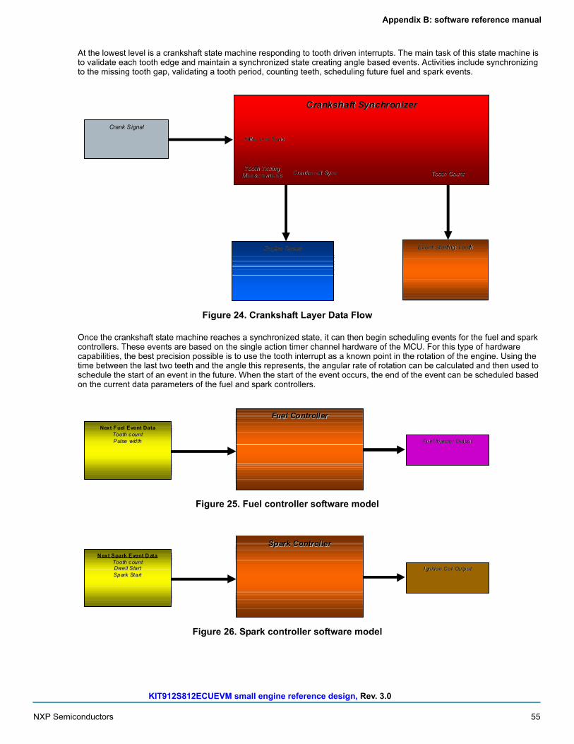
KIT912S812ECUEVM small engine reference design, Rev. 3.0
NXP Semiconductors 55
Appendix B: software reference manual
At the lowest level is a crankshaft state machine responding to tooth driven interrupts. The main task of this state machine is to validate each tooth edge and maintain a synchronized state creating angle based events. Activities include synchronizing to the missing tooth gap, validating a tooth period, counting teeth, scheduling future fuel and spark events.
CCrraannkksshhaafftt SSyynncchhrroonniizzeerr
EEvveenntt SSttaarrttiinngg TTooootthh
TTooootthh CCoouunntt
EEnnggiinnee SSppeeeedd
TTooootthh TTiimmiinngg MMeeaassuurreemmeennttss
CCrraannkk SSiiggnnaall
FFiill tteerr aanndd SSyynncc
CCrraannkksshhaafftt SSyynncc
Figure 24. Crankshaft Layer Data Flow
Once the crankshaft state machine reaches a synchronized state, it can then begin scheduling events for the fuel and spark controllers. These events are based on the single action timer channel hardware of the MCU. For this type of hardware capabilities, the best precision possible is to use the tooth interrupt as a known point in the rotation of the engine. Using the time between the last two teeth and the angle this represents, the angular rate of rotation can be calculated and then used to schedule the start of an event in the future. When the start of the event occurs, the end of the event can be scheduled based on the current data parameters of the fuel and spark controllers.
FFuueell CCoonnttrroolllleerr Next F uel Event Data
TT ooootthh ccoouunntt PPuull ssee wwiiddtthh FF uueell IInnjjeeccttoorr OOuuttppuutt
Figure 25. Fuel controller software model
SSppaarrkk CCoonnttrroolllleerr N ext Spark Event D ata
TT ooootthh ccoouunntt DD ww eellll SSttaarrtt SSppaarr kk SSttaarrtt
IIggnn iitt iioonn CCooiill OOuuttppuutt
Figure 26. Spark controller software model

KIT912S812ECUEVM small engine reference design, Rev. 3.0
56 NXP Semiconductors
Appendix B: software reference manual
New data related to when the fuel and spark events occur and for how long, are determined by the engine management task. The basis of this new data is a table look up using engine speed and load data provided by the user management task. Once the table look up takes place, any modifiers to the base table look up can then be added to create a value for use by the fuel or spark controller. To prevent complications and undesired operation, any new data calculated by engine management goes into a variable not be loaded by the fuel or spark controller until the current event completes. This lockout mechanism prevents malicious modification to fuel or spark timing during a fuel or spark event.
EEnnggiinnee MMaannaaggeemmeenntt LLOOAA DD RRPPMM
AAddddeerr vvaa lluueess NN eexxtt FFuu ee ll aanndd SS ppaarrkk
EEvvee nn tt SScchheedd uu lliinngg
BBaassee ttaabbllee llooookk uupp FF iinn aa ll vvaa lluuee ccaa llccuu llaattiioonn
Figure 27. Engine management software model
All data collection is performed by the data management task, with two exceptions: engine speed and optionally MAP data. As the crankshaft controller uses tooth period data, it makes sense for it to collect this data for use. Measuring MAP at specific teeth has strong benefits to the system and allows four-cycle synchronization without a cam sensor. The data management task is designed to collect data at a periodic rate and fill data buffers. Once the data buffers are full, the user can then run filter algorithms to provide user management with conditioned data.
DDaattaa MMaannaaggeemmeenntt
Raw Module Inputs BBaatttteerryy vvoollttaaggee
MMAAPP TTPPSS
EEnnggiinnee TTeemmppeerraattuurree AAiirr TTeemmppeerraattuurree IIggnniitt iioonn SSwwiittcchh CClluuttcchh SSwwiittcchh
DDaattaa BBuuff ffeerrss FFiilltteerreeddSSiiggnnaall DDaattaa
UUsseerr MMaannaaggeemmeenntt
Figure 28. Data management software model
The main system control is performed in the user management task. All engine control strategy and operator interface control is in this function. A basic state machine is included in the new project as well as the demo application. This application state machine is based on engine speed and is divided into 5 engine conditions: INIT, STOP, START, RUN, OVERRUN. Each of these states represents a typical operating condition an engine user/operator would like the application to manage. The conditions for going between the states and how it impacts the lower level controllers is the heart of the application that is to be created.

UUsseerr MMaannaaggeemmeenntt
Analog Data TTPPSS
EEnnggiinnee TTeemmpp MMAAPP OO22
IInnggiittiioonn SSww iittcchh BBaatttteerryy VVooll ttaaggee
Filtered AAnnaalloogg SSiiggnnaallss
EEnnggiinnee MMaannaaggeemmeenntt
CalculationsRRPPMM LLOOAADD
MMooddiiffiieerrss
RRaaww RRPPMM DDaattaa
Filtered RRPPMM DDaattaa
FFuueell aanndd SSppaarrkk CCoonnttrroolllleerrss
Enable FFuueell IInn jjeeccttoorrss IIggnniittiioonn CCooiillss
KIT912S812ECUEVM small engine reference design, Rev. 3.0
NXP Semiconductors 57
Appendix B: software reference manual
Figure 29. User management software model
15.2 Building application
Creating a new engine control strategy takes significant experience and knowledge. It is recommended to work with one of the demo applications to get a feel for a basic application using this software before creating a new one. If choosing to work with a ground up application or a demo one, there are several files that are intended for use: User management.c, engine management.c, and data management.c. Each file also has an associated header file. Additionally, each file is designed to contain a single task that is periodically executed. These tasks are user management(), engine management(), and data management(). The file Tasks.h is used to determine when each of these application tasks are called and should be modified by the user to customize the application. Tasks are broken out into 1.0 ms, 2.0 ms, 10 ms, 50 ms, and 100 ms function calls. The scheduler is very simple and the user must take into account the real time aspects of making these function calls.
15.2.1 User files
The software architecture allows the user to work with four C-code files to create a custom engine control application, User management, data management, engine management, and application maps. Each of these files has a header file associated with it as well for declaring functions and making definitions specific to the application. Each of these files, with the exception of the applications maps, has a specific function call associated with it that is invoked by the task scheduler. The scheduling of these tasks can be modified in the tasks.h file as discussed previously. The tasks.h file should include a function call to each of the user functions: user_management(), data_management(), and engine_management(). These user functions provide interaction with the low level driver functions necessary to control an engine.
15.2.2 user_management()
This function provides the interface between the engine user/operator and the engine control software. The highest level of control is performed through this function. It must take the user inputs and turn them into data for engine control as well as maintain basic operating conditions related to engine's current operating point. For example, a fundamental user control is the throttle. user_management() takes the throttle position data and provides this data to the fuel and spark controllers so the fuel and spark is adjusted for the current throttle position. Another fundamental user control is the engine kill switch. The ability of the user to shut off the engine at anytime must be maintained through the user_management() function.
Examples of a more complete user_management() function is provided in the example application. This examples use a state machine approach as running an engine has natural control states desired by most users. When getting started, it may beneficial to keep it simple and have a minimal number of inputs. This allows the designer to get familiar with the entire software architecture before getting into a more complex application.
KIT912S812ECUEVM small engine reference design, Rev. 3.0
58 NXP Semiconductors
Appendix B: software reference manual
15.2.3 Data_management()
All inputs to the system are collected by the data_management() function. There are two exceptions. Engine tooth/position data is handled specifically by the low level crank position functions. Also, the MAP signal may be defined to be collected on a tooth basis, not a time basis, which is defined in the application header file.
Digital and analog signals are collected and filtered by the data_management() task. Each signal must be defined and configured in the application header file. The data_management() must then collect the data and filter the data when buffers are full. The filtered data can then be used by user_management().
15.2.4 Engine_management()
The interface to the spark and fuel controllers is through the engine_management() task. Using the RPM and load data provided by the user_management() and crank position function, the engine_management() task makes function calls which perform a table look up of fuel and spark parameters based on the current operating point. These parameters can then be compensated based on other modifiers determined by the user_management() and then sent to the fuel and spark controllers for use on the next fuel or spark event.
A lock out mechanism exists between the fuel and spark controllers and the engine_management() function to prevent undesired operation. The fuel and spark controllers create events based on a current variable. engine_management() can only modify a next variable. When a fuel or spark event completes, the current variable is updated with the next variable.
15.2.5 Application maps
The table look up performed by the engine_management() task works with the application map source and header files. These two files create the fuel and spark tables used to control the engine. The header file is used to configure the size of the tables. The C source file contains the actual data for the table look up procedure. In addition to the table parameters, the values associated with the table indices must also be created. This includes a data array of the RPM values and an array of the load values corresponding to the indices of the fuel and spark tables. All data in the application maps is based on microcontroller timer units, not engineering units. This is noted in the example files. As a fundamental exercise in running an engine, these tables must be created based on the engine and system design. A starting point can be obtained by collecting data from an existing engine controller running the same engine or by engine modeling software capable of creating a baseline volumetric efficiency map.
15.2.6 Low Level Driver Files
The software architecture for the example application uses a hardware abstraction layer that removes details of working with the S12XS microcontroller. As a result, exercising the signals of the ECU do not require specific references to MCU signals or peripherals. However, it is worth noting that there are limitations and simple tasks at an application level may have significant overhead associated with them. For example, the S12 is a 16-bit microcontroller not having a floating point unit. Use of 32-bit data and floating point numbers should be extremely limited and is not recommended for highest performance. Also it is important to note the reference design is a system and modifying engine control signals may require interaction with another integrated circuit. This type of interaction and system architecture results in many low level software drivers behind the scenes. These drivers provide high level functionality for the application and are a key to rapid application development. While it is not vital to knowing all the low level functions, if is important during the debugging phase they exist as stepping through them occur.
KIT912S812ECUEVM small engine reference design, Rev. 3.0
NXP Semiconductors 59
References
16 References
16.1 Support
Visit www.nxp.com/support for a list of phone numbers within your region.
16.2 Warranty
Visit www.nxp.com/warranty to submit a request for tool warranty.
NXP.com Support Pages URL
MM912_S812Product Summary Page
http://www.nxp.com/webapp/sps/site/prod_summary.jsp?code=MM912_S812
S12XSProduct Summary Page
http://www.nxp.com/webapp/sps/site/prod_summary.jsp?code=S12XS
MM33812Product Summary Page
http://www.nxp.com/webapp/sps/site/prod_summary.jsp?code=MC33812
Analog Home Page http://www.nxp.com/analog
Automotive Home Page http://www.nxp.com/automotive

KIT912S812ECUEVM small engine reference design, Rev. 3.0
60 NXP Semiconductors
Revision history
17 Revision history
Revision Date Description of changes
1.0 2/2013 • Initial Release
2.0 4/2013 • Added Jump Start link for downloading software and/or documents.
3.0 3/2016• Updated Figure 1, Figure 2 and Figure 6• Updated style and format

Information in this document is provided solely to enable system and software implementers to use NXP products. There
are no expressed or implied copyright licenses granted hereunder to design or fabricate any integrated circuits based on
the information in this document. NXP reserves the right to make changes without further notice to any products herein.
NXP makes no warranty, representation, or guarantee regarding the suitability of its products for any particular purpose,
nor does NXP assume any liability arising out of the application or use of any product or circuit, and specifically disclaims
any and all liability, including without limitation, consequential or incidental damages. "Typical" parameters that may be
provided in NXP data sheets and/or specifications can and do vary in different applications, and actual performance may
vary over time. All operating parameters, including "typicals," must be validated for each customer application by the
customer's technical experts. NXP does not convey any license under its patent rights nor the rights of others. NXP sells
products pursuant to standard terms and conditions of sale, which can be found at the following address:
http://www.nxp.com/terms-of-use.html.
NXP, the NXP logo, Freescale, the Freescale logo, CodeWarrior, Kinetis, Processor Expert, and SMARTMOS are
trademarks of NXP B.V. All other product or service names are the property of their respective owners. All rights
reserved.
© 2016 NXP B.V.
How to Reach Us:Home Page: NXP.com
Web Support: http://www.nxp.com/support
Document Number: KT912_S812ECUUGRev. 3.0
3/2016