kondapur(v), ghatkesar(m), medchal(dist) subject name
TRANSCRIPT

SAMSKRUTI COLLEGE OF ENGINEERING & TECHNOLOGY (Approved by AICTE, New Delhi & Affiliated to JNTUH.)
Kondapur(V), Ghatkesar(M), Medchal(Dist)
Subject Name: Electronic Circuit Analysis
Prepared by (Faculty (s) Name): M.SREENIVASULU
Year and Sem, Department:II & II SEM, ECE
UNTI-I : MULTISTAGE AMPLIFIERS
Important Points:
1. An Amplifier circuit is the one, which changes the characteristics of the input signal, when delivered
the output side. The modification in the characteristics of the input signal can be with respect to voltage,
current, power or phase. Anyone or all these characteristics power, or phase may be changed by the
amplifier circuit.
2. A Single-stage Amplifiers has only one transistor circuit and Multi-stage Amplifiers has multiple
transistor circuit, which provides single -stage amplification and multi-stage amplification respectively.
3. The amplifier circuit that increases the voltage level of the input signal, is called as Voltage amplifier
and the amplifier that increases the power level of the input signal, is called as Power amplifier.
4. When the input signal is so weak so as to produce small fluctuations in the collector current compared
to its quiescent value, the amplifier is known as Small signal amplifier.
5. When the fluctuations in collector current are large i.e. beyond the linear portion of the characteristics,
the amplifier is known as large signal amplifier.
6. The amplifier circuit that amplifies the signals that lie in the audio frequency range i.e. from 20Hz to
20 KHz frequency range is called as audio amplifier.
7. The amplifier circuit that amplifies the signals that lie in a very high frequency range, is called as
Power amplifier.
8. A Multi-stage amplifier circuit that is coupled to the next stage using resistor and capacitor (RC)
combination can be called as a RC coupled amplifier.
9. A Multi-stage amplifier circuit that is coupled to the next stage, with the help of a transformer, can be
called as a Transformer coupled amplifier.
10. A Multi-stage amplifier circuit that is coupled to the next stage directly, can be called as a direct
coupled amplifier.
11. In Multi-stage amplifiers, the output of first stage is coupled to the input of next stage using a
coupling device. These coupling devices can usually be a capacitor or a transformer. This process of
joining two amplifier stages using a coupling device can be called as Cascading.
12. The range of frequencies over which the gain (voltage gain or current gain) of an amplifier is equal to
and greater than 0.707 times the maximum gain is called the bandwidth
SAMSKRUTI COLLEGE OF ENGINEERING & TECHNOLOGY (Approved by AICTE, New Delhi & Affiliated to JNTUH.)
Kondapur(V), Ghatkesar(M), Medchal(Dist)
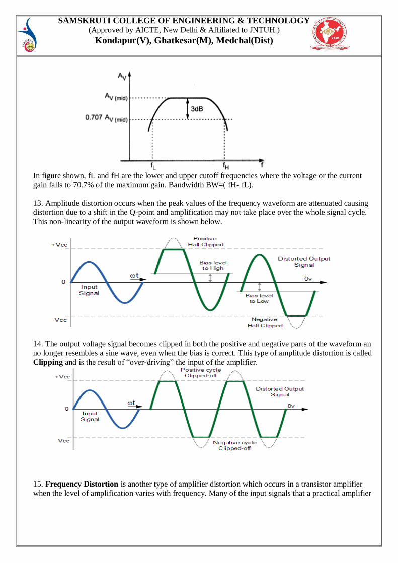
In figure shown, fL and fH are the lower and upper cutoff frequencies where the voltage or the current
gain falls to 70.7% of the maximum gain. Bandwidth BW=( fH- fL).
13. Amplitude distortion occurs when the peak values of the frequency waveform are attenuated causing
distortion due to a shift in the Q-point and amplification may not take place over the whole signal cycle.
This non-linearity of the output waveform is shown below.
14. The output voltage signal becomes clipped in both the positive and negative parts of the waveform an
no longer resembles a sine wave, even when the bias is correct. This type of amplitude distortion is called
Clipping and is the result of “over-driving” the input of the amplifier.
15. Frequency Distortion is another type of amplifier distortion which occurs in a transistor amplifier
when the level of amplification varies with frequency. Many of the input signals that a practical amplifier

SAMSKRUTI COLLEGE OF ENGINEERING & TECHNOLOGY (Approved by AICTE, New Delhi & Affiliated to JNTUH.)
Kondapur(V), Ghatkesar(M), Medchal(Dist)
will amplify consist of the required signal waveform called the “Fundamental Frequency” plus a number
of different frequencies called “Harmonics” superimposed onto it.
16. Phase Distortion or Delay Distortion is a type of amplifier distortion which occurs in a non-linear
transistor
amplifier when there is a time delay between the input signal and its appearance at the output.
17. The cascode amplifier is combined common-emitter and common-base. The cascode improves input–
output isolation (reduces reverse transmission), as there is no direct coupling from the output to input.
This eliminates the Miller effect and thus contributes to a much higher bandwidth. The use of a cascode
is a common technique for improving analog circuit performance.
18. A multi-transistor configuration called the Darlington configuration (commonly called
a Darlington pair) is a compound structure of a particular design made by two bipolar
transistors connected in such a way that the current amplified by the first transistor is amplified further by
the second one. This configuration gives a much higher current gain than each transistor taken separately.
19. Voltage gain of an amplifier is the ratio of the change in output voltage to the corresponding change
in the input voltage.
AV= ΔV0 / ΔVI
20. Current gain of an amplifier is the ratio of the change in output current to the corresponding change in
the input current
AI= ΔI0 / ΔII
21. Power gain of an amplifier is the ratio of the change in output power to the corresponding change in
the input power. Where po and pi are the output power and input power respectively. Since power p = v ×
i, the power gain is given by
AP= PO / PI
AP= AV x AI

SAMSKRUTI COLLEGE OF ENGINEERING & TECHNOLOGY (Approved by AICTE, New Delhi & Affiliated to JNTUH.)
Kondapur(V), Ghatkesar(M), Medchal(Dist)
22. The gain-bandwidth product for an amplifier is the product of the amplifier's bandwidth and
the gain at which the bandwidth is measured.
23. Unity gain band width is the frequency at which the output signal is reduced by −3 dB. The
amplifier is tested in a unity-gain configuration, with a small signal applied, usually 200 mV p-p. A low
level signal is used to determine bandwidth because this eliminates the effects of slew rate limit on the
signal.
IMPORTANT QUESTIONS
2-Marks Questions
1. Why is a CE amplifier widely used? List down its main limitations. (Nov-2017 R-13)
2. What are the typical values of h-parameters of CE configuration? (Nov-2017 R-13)
3. What is fT of a BJT? (Nov-2017 R-13)
4. Draw a small signal low frequency model of a transistor. (Dec-2017 R-15)
5. State dual of Miller’s theorem and also write its applications. (Dec-2017 R-15)
6. What is unity crossover frequency?. (Dec-2017 R-15)
7. Define a short circuit gain of a transistor in CE configuration at high frequencies. (Dec-2017 R-15)
8. Draw the circuit diagram of Darlington Pair. (April-2018-R-15)
9. What is the expression for harmonic distortion in single stage amplifiers? (April-2018-R-15)
10. Define Gain-Bandwidth Product in detail. (April-2018-R-15)
11. How the amplifiers are classified? (Dec-2018-R-15)
12. State and prove Miller’s theorem. (Dec-2018-R-15)
13. What is gain bandwidth product? (Dec-2018-R-15)
14. Why emitter bypass capacitor is needed? (Dec-2018-R-15)
5-Marks Questions
1. a) Draw the CE amplifier with un bypassed emitter resistance and derive expression for Ri and Av.
b) A transistor in CB circuit has the following set of ‘h’ parameters. hib = 20, hfb = 0.98,
hrb =3×10⁻⁴, hob = 0.5×10⁻⁶. Find the values if Ri, Ro, Ai and Av, if Rs = 600Ω and RL = 1.5 kΩ.
(Nov-2017 R-13) 2. a) Draw the Darlington circuit and derive the expressions for the overall current gain, voltage gain,
input impedance and output impedance.
b) With the help of a neat circuit diagram describe the working of a cascade amplifier.
(Nov-2017 R-13) 3. a) Draw the hybrid-П model of common emitter configuration and describe each component in the П-
model.
b) Derive the equation for voltage gain bandwidth product for CE amplifier. (Nov-2017 R-13) 4. a) Discuss the effect of different types of loads to a common source MOS amplifier.

SAMSKRUTI COLLEGE OF ENGINEERING & TECHNOLOGY (Approved by AICTE, New Delhi & Affiliated to JNTUH.)
Kondapur(V), Ghatkesar(M), Medchal(Dist)
b) Draw the CS FET amplifier equivalent circuit looking into the drain and find its gain and output
impedance. (Nov-2017 R-13) 5. a) The h parameters of a transistor used in single stage amplifier circuit are hic = 1100, hrc =1, hfc==51 and
hoc=25μA. Determine the amplifier parameters for CC configuration when RS=RL=10K.
b) For any single-stage amplifier express input resistance in terms of current gain and
H-parameters only. (Dec-2017 R-15)
6. a) Derive the bandwidth of a multistage amplifier, assuming that each stage has same upper and lower cut
off frequencies.
b) For the two stage amplifier of the figure 1, calculate the input and output impedance, and the
individual and overall voltage gains. Assume hfe =50, hie=1.1kΩ, hre = hoe= 0. (Dec-2017 R-15)
7. a) Discuss about effect of Cb on frequency response of RC coupled amplifier.
b) Draw the circuit diagram of Direct Coupled Amplifier and explain its operation in detail.
(April-2018-R-15)
8. a) With a neat circuit diagram. Explain about Boo-Strap emitter follower amplifier.
b) Derive the Analysis of CE amplifier with Emitter Resistance and explain its operation along with
circuit diagram. (April-2018-R-15)
9. a) Find the voltage gain, input and output resistances of a emitter follower at high
Frequencies.
b) A common source amplifier uses a MOSFET with the following parameters gm=1.5mA/V,
rd=40kohms, Cgs=3pF, Cds=1pF, Cgd=3.2pF. The value of Rd=200Kohms. The amplifier
operates at 30KHz. Find Voltage gain, input resistance, output resistance and input capacitance.
(April-2018-R-15)
10.a) Draw the circuit diagram of Common source amplifier with Resistive load and explain its
operation.
b) Derive the expression for fT of a transistor in detail. (April-2018-R-15)
11.a) Draw the equivalent circuit for the CE and CC configurations subject to the restriction that
RL = 0. Show that the input impedance of the two circuits are identical.
b) The transistor amplifier shown in figure 1 uses a transistor with typical h parameter values.
Calculate Ai, AV, AVs, Ro and Ri.
12.a) Draw the circuit diagram of Darlington emitter follower and derive the expression for input
impedance.
b) Explain the working of cascade amplifier with neat circuit diagram.

SAMSKRUTI COLLEGE OF ENGINEERING & TECHNOLOGY (Approved by AICTE, New Delhi & Affiliated to JNTUH.)
Kondapur(V), Ghatkesar(M), Medchal(Dist)
13.a) Draw the hybrid π equivalent circuit of a transistor in CE configuration and explain the various
parameters in it.
b) A transistor biased at 5mA, 10V, hie =600Ω, hfe=100, CC=3pF and current gain of 10 at a
frequency of 20MHz. Find β cut off frequency, gain band width product, Ce, rb′e and rbb′.
(Dec-2017 R-15)
14.a) A transistor biased at 20mA, 20V, it has the h-parameters at room temperature hie =500Ω, hfe=100,
hre =10-4, hoe =4×10⁻⁵℧. It has fT =50MHz and CC=3pF. Find all the values of hybrid π components.
b) The 3-db bandwidth of an amplifier extends from 20 Hz to 20 kHz. Find the frequency range over
which the voltage gain differs by only 1 dB from the mid band value. (Dec-2017 R-15)
Objective Type Questions:
1. The bandwidth of an amplifier can be increased by [ b ]
a) Decreasing the capacitance of its bypass capacitors
b) Minimizing the stray capacitance
c) Increasing the input signal frequency
d) Cascading it
2. .The main reason for the variation of amplifier gain with frequency is [ a ]
a) The presence of capacitance internal and external
b) due to inter stage transformation
c) The logarithmic increase in its output power
d) Miller effect
3. The emitter of a CE amplifier has no AC voltage because of the [ c ]
a) DC voltage unit b) Bypass Capacitor
c) Coupling capacitor d) load resistance
4. Typical value of hie is [ a ]
a) 1k b)25k c)50k d)100k
5. A CC-Amplifier has highest __________ but lowest ________. [ c ]
a) Voltage Gain and input resistance b) output resistance and Current Gain
c) Current gain and power gain d) None of the above
6 In the initial stages of a multi stage amplifier, we use [ a ]
a) RC coupling b) transformer coupling c) direct coupling d) None
7. The bandwidth of a single stage amplifier is ___ that of a multi stage amplifier. [ a ]

SAMSKRUTI COLLEGE OF ENGINEERING & TECHNOLOGY (Approved by AICTE, New Delhi & Affiliated to JNTUH.)
Kondapur(V), Ghatkesar(M), Medchal(Dist)
a) more than b)less than c)same as d)none
8.In a RC coupled amplifier, which of the following component is mainly responsible for harmonic distortion
of the signal [ d ]
a)Biasing resistor b)coupling capacitor c)power supply d)Transistor
9. The darlington pair consists of the following two stages [ d ]
a) CE,CC b) CE,CB c) both CE d)both CC
10.The gain bandwidth product of a two stage amplifier is [ b ]
a) Same as that of single stage b) Greater than that of single stage
c) Less than that of single stage d) Product of two gain bandwidth products of each stage
11. In a two stage cascaded amplifier, each of two cascaded stages has a voltage gain of 30 then the overall
gain is __________ [a]
a) 900 b) 0 c)60 d) 1
12) Cascode amplifier is combination of ___________________. [ c ]
a) CC-CB B)CB-CC C)CB-CE D) NONE
13) Why do we go for multi stage amplifiers? ___________________ [ b ]
a) For high input impedance b) for high gain
c) For high output impedance d)None

SAMSKRUTI COLLEGE OF ENGINEERING & TECHNOLOGY (Approved by AICTE, New Delhi & Affiliated to JNTUH.)
Kondapur(V), Ghatkesar(M), Medchal(Dist)
UNTI-II
FEEDBACK AMPLIFIERS
Important Points:
1. The process of injecting a fraction of output energy of some device back to the input is known as
feedback. The noise in the output of an amplifier is undesirable and must be kept to as small a level as
possible. The noise level in amplifiers can be reduced considerably by the use of negative feedback.
2 The amplifier introduces a phase shift of 180° into the circuit while the feedback network is so
designed that it introduces no phase shift (i.e., 0° phase shift). The result is that the feedback voltage Vf is
180° out of phase with the input signal Vin.
3.Depending upon whether the feedback energy aids or opposes the input signal, there are two basic
types of feedback in amplifiers i.e positive feedback and negative feedback. The block diagram of
Feedback amplifier is shown in the figure below.
4. The gain of the amplifier is the ratio of output voltage Vo to the input voltage Vi. the feedback
network extracts a voltage Vf = β Vo from the output Vo of the amplifier.This voltage is added for
positive feedback and subtracted for negative feedback, from the signal voltage Vs. Now,
Vi = Vs+Vf = Vs+βVo
Vi = Vs−Vf = Vs−βVo
The quantity β = Vf/Vo is called as feedback ratio or feedback fraction.
5. When the feedback energy (voltage or current) is in phase with the input signal and thus aids it, it is
called positive feedback. This is illustrated in Fig.. Both amplifier and feedback network introduce a
phase shift of 180°. The result is a 360° phase shift around the loop, causing the feedback voltage Vf to be
in phase with the input signal Vin.

SAMSKRUTI COLLEGE OF ENGINEERING & TECHNOLOGY (Approved by AICTE, New Delhi & Affiliated to JNTUH.)
Kondapur(V), Ghatkesar(M), Medchal(Dist)
6. The positive feedback increases the gain of the amplifier. However, it has the disadvantages of
increased distortion and instability. Therefore, positive feedback is seldom employed in amplifiers. One
important use of positive feedback is in oscillators.
7. When the feedback energy (voltage or current) is out of phase with the input signal and thus opposes
it, it is called negative feedback. This is illustrated in Fig.. As you can see, the amplifier introduces a
phase shift of 180° into the circuit while the feedback network is so designed that it introduces no phase
shift (i.e., 0° phase shift). The result is that the feedback voltage Vf is 180° out of phase with the input
signal Vin.
8. The feedback Amplifiers are classified as follows
i. Voltage series feedback.
ii. Voltage shunt feedback.
iii. Current shunt feedback.
iv. Current series feedback.
9. If the feedback signal is taken across RL, it is a Vo or so it is Voltage feedback.
10.If the feedback signal is taken in series with the output terminals, feedback signal is proportional to I0
, So it is current feedback.
11. If the feedback signal is in series with the input, it is series feedback.
12.If the feedback signal is in shunt with the input, it is shunt feedback.
13. The general characteristics of the Negative feedback amplifier are
Stability of gain is improved
Reduction in Distortion
Reduction in noise
Increase in input impedance
decrease in output impedance
Improves frequency response
SAMSKRUTI COLLEGE OF ENGINEERING & TECHNOLOGY (Approved by AICTE, New Delhi & Affiliated to JNTUH.)
Kondapur(V), Ghatkesar(M), Medchal(Dist)
IMPORTANT QUESTIONS
2-Marks Questions
1. State Miller’s theorem. (Nov-2017 R-13)
2. What are the advantages of negative feedback? (Nov-2017 R-13)
3. What is Class-A power amplifier? (Nov-2017 R-13)
4. Classify power Amplifiers. (Nov-2017 R-13)
5. What is effect of negative feedback on amplifier gain? (Dec-2017 R-15)
6. Draw the Small signal model of MOS amplifier. (April-2018-R-15)
7. Explain different Classification of Feedback Amplifiers (April-2018-R-15)
8. How the stability of amplifier will affect by negative feedback amplifier? (Dec-2018-R-15)
5-Marks Questions
1. a) Explain the principle of negative feedback in amplifiers. Show quantitatively the effect of negative
feedback on (i) Gain (ii) Stability (iii) Noise (iv) Distortion.
b) Show that current–series negative feedback increases the input impedance and increases the output
impedance. (Nov-2017 R-13)
2. a) The amplifier of figure 2 uses a FET with IDSS =3mA, Vp= -3V, rd>>Rd. Find the quiescent drain
current, quiescent drain to source voltage and AV.
b) Derive the equation for voltage gain of a CS FET amplifier. (Dec-2017 R-15)
3.a) An amplifier has an open loop voltage gain of 1000 and delivers 10W output with 10% second
harmonic distortion when the input is 10mV. Find the distortion of 60dB of negative feedback is applied.
b) Calculate Avf = V0/Vs, Rif and Rof for the circuit shown in figure 3 use typical h parameter values.
Rs=RC=10K and Re=1K. (Dec-2017 R-15)
4.a) Draw the block diagrams of four types of negative feedback amplifier circuits and explain the
advantages and disadvantages with necessary derivations.
b) Explain why RC Phase shift oscillators are not used at high frequencies. (April-2018-R-15) 5.a) Calculate the voltage gain of the FET amplifier shown in the figure 2. Assuming blocking capacitor to
be large.gm=4mA/V and rd =5K.
b) Sketch the small signal model of a CD FET amplifier and derive equation for the voltage gain.
6.a) Draw the negative feedback topologies and explain them.
b) An open loop amplifier has a midband gain of 500 and a pass band from 50Hz to 50KHz. Find
voltage gain and cut off frequencies if 10% of output voltage is fed back.

SAMSKRUTI COLLEGE OF ENGINEERING & TECHNOLOGY (Approved by AICTE, New Delhi & Affiliated to JNTUH.)
Kondapur(V), Ghatkesar(M), Medchal(Dist)
OBJECTIVE TYPE QUESTIONS :
1 In a CE amplifier, the unbypassed emitter resistance provides [c]
a) Voltage shunt feedback b)Current series feedback
c) Negative voltage feedback c) Positive current feedback
2 .Negative feedback in amplifier [ b ]
a) improves SNR at the input b) improves SNR at the output
c) Increases distortion c) None of the above
3.The gain of an amplifier with feedback is ______. [ a ]
a) A/1+Aβ b) β/1+βa c) β/1-βa d) A/1-Aβ
4. In an ideal voltage amplifier, the values of Ri & R0 are ________________ [b]
a) 0, ∞ b) ∞,0 c) 0,0 d) ∞, ∞
5. Negative feedback in amplifier [ b ]
(a) Improves SNR at the input (b) improves SNR at the output
(c) Increases distortion (d) None of the above
6. In voltage shunt feedback, the input impedance [ b]
a)Increases b)Decreases
c)Depends on dc voltage applied d) Depends on frequency of operation
7. One of the effects of negative feedback in amplifier is to [b]
a) Increase the noise b) decrease the hormonic distortion
c )Increase the voltage gain d)Decrease the bandwidth
8. Negative feedback in amplifier [d]
a) Increase the gain stability b) decrease distortion and noise level
c ) Increase input impedance and decrease output impedance d)All of these
9. The input impedance of an amplifier can be increased from 2 kilo ohm to 250 kilo ohm by introducing
[c]

SAMSKRUTI COLLEGE OF ENGINEERING & TECHNOLOGY (Approved by AICTE, New Delhi & Affiliated to JNTUH.)
Kondapur(V), Ghatkesar(M), Medchal(Dist)
a) Shunt current negative feedback b) Shunt voltage negative feedback
c ) Series current negative feedback d) None of these
10) The negative feedback as an amplifier [d]
a) Increase the voltage gain b) decrease the voltage gain
c ) stabilize the voltage gain d) both B and C are correct