korea-france joint symposium 2014 - qmmrc.net · korea-france joint symposium 2014 june 24 (tue) -...
TRANSCRIPT

KOREA-FRANCE Joint Symposium 2014
June 24 (Tue) - June 27 (Fri), 2014
Topic : Material Design and Engineering
KOREA-FRANCE Joint Symposium 2014 (The 3rd Symposium)
Advisory Committee : Marc Drillon (IPCMS/CNRS, France)Patrick Maestro (Solvay)Alain Fort (IPCMS/CNRS, France), Hiroyuki Sasabe (Kyushu University, Japan)
Organizing Committee : Stefan Haacke (IPCMS/CNRS, France)Andre-Jean Attias (UPMC, France)Jeong Weon Wu (Ewha W. Univ., Korea),Eun Kyoung Kim (Yonsei Univ., Korea)
Program Committee : Carlo Massobrio (IPCMS/CNRS, France)Christian Meny (IPCMS/CNRS, France)Jean-Charles Ribierre (Kyushu Univ.)William Jo (Ewha W. Univ., Korea)
Local Committee : Soon-Ho Chang (Solvay Korea Co LTD, Korea)Dong-Wook Kim (Ewha W. Univ., Korea)

Program
June 24 (Tue) June 25 (Wed) June 26 (Thur) June 27 (Fri)
KOREA-FRANCE Joint SymposiumTopics : Material Design and Engineering
8:00 - 9:00 Registration 8:00-16:00
Session Chair Marc Drillon (IPCMS, Strasbourg)
Alain Fort (IPCMS, Strasbourg)
Stefan Haacke (IPCMS, Strasbourg)
8:40 - 9:15 [MOF-1]Keynote
Gérard Férey (University of Versailles)
From interesting to useful: the multiple richnesses of hybrid porous
solids
[OOE-5]Stefan Haacke(IPCMS/CNRS)
Ultrafast photo-physics of organic nanostructures: New Materials for
organic solar cells
[CS-1]Fabrizio Cleri
(IEMN, University of Lille I)
Self-assembly of organic molecules on semiconductor surfaces
9:15 - 9:50
[OOE-6]Chihaya Adachi
(Kyushu University)
High efficiency organic light-emitting diodes using delayed fluorescence
[CS-2]Hyoung Joon Choi(Yonsei University)
First-principles calculation of effects of magnetic impurities on topological
surface states
9:50 - 10:25
[MOF-2]Philip Llewellyn
(Aix Marseille University)
Towards a screening of MOFs for gas related applications
[OOE-7]Soo Young Park
(Seoul National University)
Thermally-Assisted Delayed Fluorescence Mediated by
Excited-State Proton Transfer
[CS-3]Sang Soo Han
(KIST) Improved Design of Metal-Organic
Frameworks for Efficient Gas Adsorption by Multi-scale
Simulation with Strong Accuracy
10:25 - 10:40 Break Break Break
Session Chair Pascal Andre (LIA-IPCMS)
Andre Jean Attias (UPMC, Paris)
Pierre Rabu (IPCMS, Strasbourg)
10:40 - 11:15
[MOF-3]Jong-San Chang
(KRICT)
Porous Metal(III) Carboxylates as Multifunctional Adsorbents and
Catalytic Materials
[SMF-1] Sergio Tatay Aguilar
(Valencia University, Spain)
Molecular Spintronics
[CS-4]
Young Woo Son(Korea Institue for Advanced
Study)
Origin of anomalous water permeation through graphene oxide
membrane
11:15 - 11:50
[MOF-4]Kyung Byung Yoon(Sogang University)
Zeolites and the environmental issues
[SMF-2] Yoon Hee Jeong
(POSTECH)
Electronic ferroelectricity and multiferroic domains in LuFe2O4
observed by scanning probe microscopy
[CS-5]Assil Bouzid
(IPCMS/CNRS)
Structural changes on GexSe1-x chalcogenides under the effect of
pressure by first principles molecular dynamics
11:50 – 12:40Lunch
11:50-13:25
[SMF-3]11:50-12:25
Nathalie Viart(IPCMS/CNRS)
Latest developments in the quest for room temperature multiferroic
thin films
Lunch
11:50-13:25
12:40 - 14:00Registration
12:40-17:45Lunch
12:25-14:00

Program
June 24 (Tue) June 25 (Wed) June 26 (Thur) June 27 (Fri)
KOREA-FRANCE Joint Symposium
Topics : Material Design and Engineering
Session Chair William Jo (Ewha W.U.)
Jeong Weon Wu (Ewha W.U.)
Jean-Charles Ribierre (Kyushu U.)
Stéphane Parola (ENS Lyon)
Opening Remark (13:55)
[OOE-1]13:25-14:00
Jang-Joo Kim(Seoul National University)
High efficiency OLEDs using phosphorescent dyes with
horizontally oriented transition dipoles
[HMF-4]13:25-14:00
Pierre Audebert(ENS Cachan)
Recent advances in tetrazines chemistry; multifunctional
molecules, nanoparticles and applications
14:00 - 14:35
[PV-1]Takuji Takahashi
(The University of Tokyo)
Photo-assisted scanning probe microscopy on CIGS solar cells
[OOE-2]Jean Charles Ribierre(Kyushu University)
Recent progress in ultraflexible organic electronics
[HMF-1] Stéphane Parola
(ENS Lyon)
Hybrid metal nanoparticles for bioimaging and optical protection
[HMF-5] Philippe Hapiot
(Universite de Rennes)
Electrochemistry as a Tool for Making Controlled
Surface Functionalizations
14:35 - 15:10
[PV-2]Thomas Heiser
(University of Strasbourg)
Solution-processed donor-acceptor bulk heterojunctions: tailoring the molecular structure to enhance the
photovoltaic performance
[OOE-3]Byung Jin Cho
(KAIST)
Application of graphene for analog and digital electronics
[HMF-2] Marc Fourmigué
(Universite de Rennes)
Halogen bonding in molecular solids: control of charge transfer
[HMF-6] Ivan Rivalta(ENS Lyon)
Tracking structure and dynamics of biological
systems by two-dimensional optical spectroscopy
15:10 - 15:45
[PV-3]Bernard Geffroy
(LICSEN/NIMBE, CEA Saclay)
Hybrid Photocathode coupling organic solar cells and MoS3
catalyst for solar hydrogen production.
[OOE-4]Anthony D'Aléo
(Aix Marseille University)
Optical Properties and Application of borondifluoride complexes
[HMF-3] Etienne Duguet
(University of Bordeaux)
Design of nanoparticles of new and complex morphology for assembly
purpose
[HMF-7] Pierre Rabu
(IPCMS/CNRS)
Hybrid interfaces in layered systems: chemistry and
functionality
15:45 - 16:00 Break Break Break Closing Remark
Session Chair Thomas Heiser (ICUBE, Strasbourg)
Dong-Wook Kim (Ewha W.U.)
Visit Solvay Korea Lab.
16:00 - 16:35
[PV-4]Sukgeun Choi
(NREL)
Optical properties of Cu2ZnSnSe4 and related compounds for
thin-film photovoltaics
Poster Session16:35 - 17:10
[PV-5]Jin Young Kim
(KIST)
Electrochemically deposited chalcogenide thin films for solar
cell application
17:10 - 17:45
[PV-6]William Jo
(Ewha W. University)
Grain boundaries of kesterite thin-films studied by Kelvin probe
force microscopy
i
Contents
KOREA-FRANCE Joint Symposium 2014
June 24 (Tue)
[PV-1] (14:00-14:35)
Photo-assisted scanning probe microscopy on CIGS solar cells ······························· 3Takuji Takahashi (University of Tokyo)
[PV-2] (14:35-15:10)
Solution-processed donor-acceptor bulk heterojunctions: tailoring the molecular structure to enhance the photovoltaic performance ···················································· 5Thomas Heiser (University of Strasbourg)
[PV-3] (15:10-15:45)
Hybrid Photocathode coupling organic solar cells and MoS3 catalyst for solar hydrogen production. ··································································································· 7Bernard Geffroy (LICSEN/NIMBE, CEA Saclay)
[PV-4] (16:00-16:35)
Optical properties of Cu2ZnSnSe4 and related compounds for thin-film photovoltaics ················································································································ 9Sukgeun Choi (NREL)
[PV-5] (16:35-17:10)
Electrochemically deposited chalcogenide thin films for solar cell application ······ 11Jin Young Kim (KIST)
[PV-6] (17:10-17:45)
Grain boundaries of kesterite thin-films studied by Kelvin probe force microscopy ················································································································· 13William Jo (Ewha W. University)

ii
June 25 (Wed)
[MOF-1] (8:40-9:50)
From interesting to useful: the multiple richnesses of hybrid porous solids ········· 15Gérard Férey (University of Versailles)
[MOF-2] (9:50-10:25)
Towards a screening of MOFs for gas related applications ··································· 17Philip Llewellyn (Aix Marseille University)
[MOF-3] (10:40-11:15)
Porous Metal(III) Carboxylates as Multifunctional Adsorbents and Catalytic Materials ····················································································································· 19Jong-San Chang (KRICT)
[MOF-4] (11:15-11:50)
Zeolites and the environmental issues ······································································ 21Kyung Byung Yoon (Sogang University)
[OOE-1] (13:25-14:00)
High efficiency OLEDs using phosphorescent dyes with horizontally oriented transition dipoles ········································································································ 25Jang-Joo Kim (Seoul National University)
[OOE-2] (14:00-14:35)
Recent progress in ultraflexible organic electronics ················································· 27Jean Charles Ribierre (Kyushu University)
[OOE-3] (14:35-15:10)
Application of graphene for analog and digital electronics ····································· 29Byung Jin Cho (KAIST)
[OOE-4] (15:10-15:45)
Optical Properties and Application of borondifluoride complexes ·························· 31Anthony D'Aléo (Aix Marseille University)

iii
June 26 (Thur)
[OOE-5] (8:40-9:15)
Ultrafast photo-physics of organic nanostructures: New Materials for organic solar cells ··················································································································· 33Stefan Haacke (IPCMS/CNRS)
[OOE-6] (9:15-9:50)
High efficiency organic light-emitting diodes using delayed fluorescence ·············· 35Chihaya Adachi (Kyushu University)
[OOE-7] (9:50-10:25)
Thermally-Assisted Delayed Fluorescence Mediated by Excited-State Proton Transfer ······················································································································ 37Soo Young Park (Seoul National University)
[SMF-1] (10:40-11:15)
Molecular Spintronics ································································································ 39Sergio Tatay Aguilar (Valencia University, Spain)
[SMF-2] (11:15-11:50)
Electronic ferroelectricity and multiferroic domains in LuFe2O4 observed by scanning probe microscopy ······················································································· 41Yoon Hee Jeong (POSTECH)
[SMF-3] (11:50-12:25)
Latest developments in the quest for room temperature multiferroic thin films ···· 43Nathalie Viart (IPCMS/CNRS)
[HMF-1] (14:00-14:35)
Hybrid metal nanoparticles for bioimaging and optical protection ························· 45Stéphane Parola (ENS Lyon)
[HMF-2] (14:35-15:10)
Halogen bonding in molecular solids: control of charge transfer ························· 47Marc Fourmigué (Universite de Rennes)
[HMF-3] (15:10-15:45)
Design of nanoparticles of new and complex morphology for assembly purpose ······················································································································· 49Etienne Duguet (University of Bordeaux)

iv
June 27 (Fri)
[CS-1] (8:40-9:15)
Self-assembly of organic molecules on semiconductor surfaces ······························ 51Fabrizio Cleri (IEMN, University of Lille I)
[CS-2] (9:15-9:50)
First-principles calculation of effects of magnetic impurities on topological surface states ·············································································································· 53Hyoung Joon Choi (Yonsei University)
[CS-3] (9:50-10:25)
Improved Design of Metal-Organic Frameworks for Efficient Gas Adsorption by Multi-scale Simulation with Strong Accuracy ·························································· 55Sang Soo Han (KIST)
[CS-4] (10:40-11:15)
Origin of anomalous water permeation through graphene oxide membrane ··········· 57Young Woo Son (Korea Institue for Advanced Study)
[CS-5] (11:15-11:50)
Structural changes on GexSe1-x chalcogenides under the effect of pressure by first principles molecular dynamics ·········································································· 59Assil Bouzid (IPCMS/CNRS)
[HMF-4] (13:25-14:00)
Recent advances in tetrazines chemistry; multifunctional molecules, nanoparticles and applications ········································································································· 61Pierre Audebert (ENS Cachan)
[HMF-5] (14:00-14:35)
Electrochemistry as a Tool for Making Controlled Surface Functionalizations ······ 63Philippe Hapiot (Universite de Rennes)
[HMF-6] (14:35-15:10)
Tracking structure and dynamics of biological systems by two-dimensional optical spectroscopy ··································································································· 65Ivan Rivalta (ENS Lyon)
[HMF-7] (15:10-15:45)
Hybrid interfaces in layered systems: chemistry and functionality ························· 67Pierre Rabu (IPCMS/CNRS)
v
Abstracts for poster presentation
June 25 (Wed) 16:00-17:45
Poster-1
Semiconductor Epsilon-Near-Zero Nano-Optics ··························································· 71Young Chul Jun (Department of Physics, Inha University, Republic of Korea)
Poster-2
Topological surface states in Bi2Te3 nanowires and nanotubes ································· 72Byung Cheol Park†, Nalae Han†, Ha-Yeong Kim‡, Sung-Jin Kim‡, Kyung Hwa Yoo† and Jae Hoon Kim†
(†Department of Physics, Yonsei University, Seoul 120-749, Republic of Korea‡Department of Chemistry and Nano Science, Ewha Womans University, Seoul 120-750, Republic of Korea)
Poster-3
Studying influence of NaF layer on Cu2ZnSnSe4 thin films by Raman scattering spectroscopy ·················································································································· 73Nguyen Thi Thu Trang, Hae-Young Shin, Gee Yeong Kim, Ju Ri Kim, William Jo, and Seokhyun Yoon* (Department of Physics, Ewha Womans University, Seoul, 120-750, Korea)
Poster-4
Resistive Switching in Ferroelectric BiFeO3 Nano-Island Based Switchable Diodes ··· 74Jihoon Jeon1, Ho-young Joo2, Yeon Soo Kim1, JinSoo Kim3, Taekjib Choi2 and BaeHo Park1*
(1 Division of Quantum Phases & Devices, Department of Physics, Konkuk University, Seoul, Korea2 Department of Nano Science & Technology, Sejong University, Seoul, Korea3 Creative Research for Graphene Electronics, Electronics and Telecommunications Research Institute, Daejeon, Korea)
Poster-5
Improvement of Nano-pipette Ion-Selective Detection Method Using Poly(vinyl chloride) Membrane ······································································································ 75Jong Wan Son, Eun Ji Kang, Tomohide Takami, Xiao Long Deng, Tomoji Kawai, and Bae Ho Park(Division of Quantum Phases and Devices, Department of Physics, Konkuk University, Seoul 143-701, Republic of Korea)
Poster-6
Structural Control on Ir(III)-Pt(II) Dyads for Photo-Hydrogen-Evolving Molecular Devices ························································································································· 76Youngkwang Kim, Dong Ryeol Whang, and Soo Young Park* (Center for Supramolecular Optoelectronic Materials, Department of Materials Science and Engineering, Seoul National University, Seoul 151-744, Korea

vi
Poster-7
Sign Change of Photoinduced Magnetoresistance in Bilayer Organic Field-Effect Transistors ····················································································································· 78Jin Hong Kim,† Song-Toan Pham,‡ Hirokazu Tada‡ and Soo Young Park(†Center for Supramolecular Optoelectronic Materials and WCU Hybrid Materials Program, Department of Materials
Science and Engineering, Seoul National University, 1 Gwanak-ro, Gwanak-gu, Seoul 151-744, Korea‡Division of Materials Physics, Graduate School of Engineering Science, Osaka University, Toyonaka 560-8531, Japan)
Poster-8
Switchable Schottky diode effect induced by electroforming bias in Mn-doped ZnO thin films ············································································································· 79YoonSeung Nam1, InRok Hwang2, ChanSoo Yoon1, JiHoon Jun1, SangIk Lee1, EunA Won1, TaeJoon Oh1, GwangTaek Oh1, TaekJib Choi3, and Bae Ho Park1
(1Dept. of Division of Quantum Phases and Devices, Konkuk University, Korea 2Electronic Materials Research Center, Future Convergence Research Division, Korea Institute of Science and Technology, Korea, 3Hybrid Materials Research Center and Faculty/Institute of Nanotechnology and Advanced Materials Engineering, Sejong University, Korea)
Poster-9
Investigation of polarized charge injection into top-emitting OLED prepared on Si(100)/MgO(100)/Fe(100)/MgO(100) multilayers ························································ 81NYUN JONG LEE1, YU JEONG BAE1, TAE HEE KIM1*, HYUNDUCK CHO2,CHANGHEE LEE2, EISUKE ITO3 (1Department of Physics, Ewha Womans University, Seoul, South Korea,2School of Electrical Engineering and Computer Science, Seoul National University, Seoul, South Korea,3Flucto-Order Functions Research Team, RIKEN Advanced Science Institute, Wako, Saitama 351-0198, Japan)
Poster-10
2D correlation analysis of the magnetic excitations in Raman spectra of HoMnO3 ························································································································ 82Thi Huyen Nguyena, Thi Minh Hien Nguyena, Xiang-Bai Chenb, In-Sang Yanga*,Yeonju Parkc and Young Mee Jungc
(aDepartment of Physics, Ewha Womans University, Seoul 120-750, KoreabDepartment of Applied Physics, Konkuk University, Chungju 380-701, KoreacDepartment of Chemistry, Kangwon National University, Chunchon 200-701, Korea)
Poster-11
Magnetism in the bilayer Hubbard model ·································································· 83Aaram J. Kim1, Gun Sang Jeon2, and MooYoung Choi1
(1Department of Physics and Astronomy and Center for Theoretical Physics, Seoul National University, Seoul 151-747, Korea2Department of Physics, Ewha Womans University, Seoul 120-750, Korea)

vii
Poster-12
Femtosecond transient absorption measurement of energy and charge transfers in discotic liquid crystalline donor-acceptor dyad and triad ··········································· 84J. H. Woo1,2, K. J. Lee1,2, Y. Xiao3, L. Mazur3,4, E. S. Kim1,2, K. Matczyszyn4, M. Samoc4, F. Mathevet3, A.-J. Attias3, J.W. Wu1,2 and J.-C. Ribierre1,2
(1Department of Physics, Ewha Womans University, Seoul, Korea2CNRS- Ewha International Research Center, Seoul, Korea3Laboratory of Polymer Chemistry, University Pierre et Marie Curie, Paris, France4Institute of Physical and Theoretical Chemistry, Wroclaw University of Technology, Wrocław, Poland)
Poster-13
Study of phase transitions in classical antiferromagnetic Heisenberg model ············ 85Miso Yun and Gun Sang Jeon* (*Department of Physics, Ewha Womans University, Seoul, Korea)
Poster-14
Surface embossed grating patterning of organic thin films, using the ultrafast laser. ······························································································································ 86Sang Min Chae, Si Woo Lee, Kuk Hyun Jo, Yong Hyun Kim1, Ji Yeon Choi1,*, Hyo Jung Kim*
(Department of Organic Material Science and Engineering, College of Engineering, Busan 609-755, Korea1Korea Institute of Machinery and Materials, 104 Sinseongno, Yuseong-Gu, Daejeon 305-343, Korea)
Poster-15
Tunneling-induced Photon Emission from ultrathin Ag nano-island ·························· 87Sanghan Kim, Jeongseok Woo, Hyungjoon Shim, and Geunseop Lee* (*Department of Physics, Inha University, Incheon 402-751, South Korea)
Poster-16
The effect of impurities (as O and In) on hysteresis and phase transition of In/Si(111)-4×1 surface ·································································································· 88Hyungjoon Shim, Yujin Jeon, Jonghoon Yeo and Geunseop Lee (Department of Physics, Inha University, Incheon,Korea)
Poster-17
Rupturing of the Hoogsteen base pairing in triplex DNA by magnetic tweezers ···· 89Il Buem Lee and Seok-Cheol Hong (Department of Physics, Korea University, Seoul, Korea)
Poster-18
Z-DNA-forming TG repeats are dynamic mechanical switches sensitive to tension and torsion. ··················································································································· 90Sook Ho Kim1, Nam-Kyung Lee2, Joon-Hwa Lee3 and Seok-Cheol Hong1
(1Department of Physics, Korea University, Seoul, Republic of Korea, 136-713.2Department of Physics, Sejong University, Seoul, Republic of Korea, 143-743.3Department of Chemistry, Gyeongsang National University, Jinju, Gyeongnam, Republic of Korea, 660-701.)

viii
Poster-19
Realization of Acoustic Superlens Using an Effective Negative Density Metamaterial slab ········································································································· 92Jong Jin Park1, K. J. B. Lee2, and Sam H. Lee1 (1Institute of Physics and Applied Physics, Yonsei University, Seoul 120-749, Korea2Department of Physics, Ewha Womnas University, Seoul 120-750, Korea)
Poster-20
Solar cells with nanostructure for ultrathin crystalline silicon photovoltaics ············ 94Yunae Cho1, Minji Gwon1, Dong-Wook Kim1,*, and Joondong Kim2
(1Department. of Physics, Ewha Womans University, Seoul, 120-750, Korea2Department of Electrical Engineering, Incheon National University, Incheon 406-772, Korea)
Poster-21
Optical Reflectance Spectra of Periodic Metal/dielectric Nanostructures ··················· 95Minji Gwon1, Yunae Cho1, Y. U. Lee1, J. W. Wu1, Dahyun Nam2, Hyeonsik Cheong2, and Dong-Wook Kim1
(1Department of Physics and Quantum Metamaterials Research Center, Ewha Womans University, Seoul 120-750, Korea2Department of Physics, Sogang University, Seoul 121-742, Korea)
Poster-22
Between Scylla and Charybdis:Hydrophobic Graphene-Guided Water Diffusion on Hydrophilic Substrates ···························································································· 96Jin-Soo Kim1,2, Jin Sik Choi1,2, Mi Jung Lee1, Bae Ho Park1, Danil Bukhvalov3, Young-Woo Son3, Duhee Yoon4, Hyeonsik Cheong5, Jun-Nyeong Yun6, Yousung Jung6, Jeong Young Park6,7 & Miquel Salmeron8
(1Division of Quantum Phases and Devices, Department of Physics, Konkuk University, Seoul 143–701, Republic of Korea, 2Creative Research Center for Graphene Electronics, Electronics and Telecommunications Research Institute (ETRI), Daejeon 305–700,Republic of Korea, 3Korea Institute for Advanced Study, Seoul 130–722, Republic of Korea, 4Electrical Engineering Division, Cambridge University, Cambridge, CB3 0FA, UK, 5Department of Physics, Sogang University, Seoul 121–742, Republic of Korea, 6Graduate School of EEWS, NanoCentury KI, Korea Advanced Institute of Science and Technology (KAIST), Daejeon 305–701, Republic of Korea, 7Center for Nanomaterials and Chemical Reactions, Institute for Basic Science (IBS), Daejeon 305–701, Republic of Korea, 8Materials Science Division, Lawrence Berkeley National Laboratory, Berkeley, CA 94720, USA.)
Poster-23
Influence of thermal annealing on the photophysical properties of pentafluorene thin film ························································································································ 98Eun Young Choi1, Loïc Mager2, Alberto Barsella2, Delphine Pitrat3, Masanobu Uchiyama4,5, Tetsuya Aoyama4, Kokou D.(Honorat) Dorkenoo2, Alain Fort2, Chantal Andraud3, Jeong Weon Wu1
and Jean Charles Ribierre1,*
(1CNRS-Ewha International Research Center, Department of Phisics, Ewha Womans University, Seoul, Korea2CNRS-IPCMS, Université de Strasbourg, 23 rue du Loess, Strasbourg, France3Ecole Normale Supérieure de Lyon/CNRS, 46 avenue d’Italie, Lyon, France4Elements Chemistry Laboratory, RIKEN, 2-1 Hirosawa, Wako, Japan5Graduate School of Pharmaceutical Sciences, The University of Tokyo, 7-3-1 Hongo, Bunkyo-ku, Tokyo, Japan*Center for Organic Photonics and Electronics Research(OPERA), Kyushu University, Fukuoka City, Japan)

ix
Poster-24
Oxidative Dimerization of (P-P)Pt(SR)2 to (P-P)Pt(μ-SR)2Pt(P-P) ···························· 100Hyokyung Jeon,1 Taejung Park,1 P. Vinothas2, and Dong-Youn Noh1,*
(1Department of Chemistry, Seoul Women’s University, Seoul 139-774, Korea2Department of Chemistry, University of Rennes I, 35000 Rennes, France)
Poster-25
Colorimetric P2Pt(dmit) sensor for Hg(II) ion(dmit: 1,3-dithiiole-2-thione-4,5-dithiolate) ···················································································································· 101Sohee Jeon and Dong-Youn Noh*(Department of Chemistry, Seoul Women’s University, Seoul 139-774, Korea)
Poster-26
Electrochemical Behaviors of Multifunctional Metal-dithiolene Complexes: (diphosphine)M(1,2-dithiolene) where M = Ni(II) and Pt(II) ··································· 103Yun-Gyeong Yi and Dong-Youn Noh* (Department of Chemistry, Seoul Women’s University, Seoul 139-774, Korea)
Poster-27
Stability study of polymerized cholesteric liquid crystal laser array ······················· 105Mi-Yun Jeong1*, Ki Soo Chung1, and Jeong Weon Wu2* (1Department of Physics and Research Institute of Natural Science, Gyeongsang National University, Jinju, Gyeongnam
660-701, South Korea 2Department of Physics and Quantum Metamaterials Research Center, Ewha Womans University, Seoul 120-750, South Korea)
Poster-28
Structural and electrical properties of BiInO3-PbTiO3 thin films grown by pulsed laser deposition ······························································································· 107Hye-Jin Jin, Seol Hee Oh, and William Jo*
(Department of Physics, Ewha Womans University, Seoul 120-750, Korea)
Poster-29
Resistive switching of charge conducting states in nickel oxide nano-dots by atomic force microscopy ···························································································· 108N. R. Lee1, W. Jo1, D. W. Kim1, C. Liu2 and C. Meny3
(1Department of Physics, Ewha Womans University, Seoul 120-750, Korea2Department of Physics, Hankuk University of Foreign Studies, Yongin 426-791, Korea)

x
Poster-30
Influence of Co content on the transport and magnetic properties of CoxFe3-xO4 thin films on MgO (100) ·························································································· 109Quang Van Nguyen1, Christian Meny2*, Duong Anh Tuan1, Yooleemi Shin1, and Sunglae Cho1
(1Department of Physics, University of Ulsan, Ulsan 680-749, Korea2Institute of Physics and Chemistry for Materials of Strasbourg, UMR 7504 UDS-CNRS, Strasbourg, 67034, France)
Poster-31
Carrier transport of Cu2ZnSn(S,Se)4 solar cell materials with various secondary phases ········································································································ 111Gee Yeong Kim, Ju Ri Kim, William Jo*, Ngyuen Thi Thu Trang, Hae-Young Shin, and Seokhyun Yoon (Department of Physics, Ewha Womans University, Seoul 120-750, Korea)
Poster-32
Enhanced magnetoresistance of Co thin films on GaAs(001) substrate ·················· 112Yooleemi Shin1, Seungmok Jeon1, Duong Anh Tuan1, Christian Meny2, and Sunglae Cho1*
(1Department of Physics and Energy Harvest Storage Research Center, University of Ulsan, Ulsan 680-749, South Korea2Institute of Physics and Chemistry of Materials of Strasbourg (IPCMS), CNRS-University of Strasbourg, UMR 7504, 23, rue du Loess, 67037 Strasbourg Cedex 02, France)
Poster-33
Reflection resonance switching in metamaterial twisted nematics cell ···················· 113Y. U. Lee, E. Y. Choi, J. H. Woo, E. S. Kim, and J. W. Wu(Ewha Womans University Department of Physics, Seoul 120-750, KOREA)
Poster-34
Structural properties of polar magnetic PbVO3 (001) thin films on LaAlO3 and SrTiO3 substrates prepared by laser ablation ···························································· 114Seol Hee Oh1), Hye-Jin Jin1), Hae-Young Shin1), Sung Jin Kang2), Seokhyun Yoon1), Miyoung Kim2), Jai-Seok Ahn3), and William Jo1)*
( 1)Department of Physics, Ewha Womans University, Seoul, Korea2)Department of Materials Science and Engineering, Seoul National University, Seoul, Korea3)Department of Physics, Pusan National University, Busan, Korea)

KOREA-FRANCE Joint Symposium 2014

KOREA-FRANCE Joint Symposium 2014 • 3
[PV-1]
Photo-assisted scanning probe microscopy on CIGS
solar cells
Prof. Takuji Takahashi
[Affiliation] The University of Tokyo, Institute of Industrial Science (IIS)
[Contact] 4-6-1 Komaba, Meguro-ku, Tokyo 153-8505
[Tel] +81-3-5452-6269
[Fax] +81-3-5452-6271
[Email] [email protected]
Curriculum Vitae[Education]
1992 Ph.D., The University of Tokyo (Japan) 1989 M.S., The University of Tokyo (Japan) 1987 B.S., The University of Tokyo (Japan)
[Positions]
2013.04~present Professor, The University of Tokyo (Japan) 1996.12~2013.03 Associate Professor, The University of Tokyo (Japan) 1992.04~1996.12 Lecturer, The University of Tokyo (Japan)
[Research Interests]
Scanning Probe Microscopy, Solar Cell Materials, Semiconductor Nanostructures

4 • KOREA-FRANCE Joint Symposium 2014
AbstractSolar cells attract a great deal of interests nowadays as important measures against the global warming. Among a lot of materials used for the solar cells, multi- or micro-crystalline materials have a big advantage in their fabrication costs. Since, however, those materials should include many grain boundaries (GBs), microscopic investigation of the behavior of the GBs is very important in order to improve their solar cell performance. To realize such investigations, we have developed the photo-assisted scanning probe microscopy methods. In this lecture, photo-assisted Kelvin probe microscopy (P-KFM) and photothermal atomic force microscopy (PT-AFM) on Cu(In,Ga)Se2 [CIGS] solar cell materials will be presented. By P-KFM, the photovoltage distribution mapping as well as the photovoltage decay measurements can be performed, while PT-AFM, in which the periodical thermal expansion induced by the intermittent light illumination is detected by AFM, enables us to investigate the non-radiative recombination properties of the photo-carriers. Using those methods, we have examined the CIGS solar cells with various Ga contents, and discuss the photo-carrier dynamics as well as their relationship with the conversion efficiency.

KOREA-FRANCE Joint Symposium 2014 • 5
[PV-2]
Solution-processed donor-acceptor bulk heterojunctions:
tailoring the molecular structure to enhance the
photovoltaic performance
Prof. Thomas Heiser
[Affiliation] University of Strasbourg, Laboratory of Engineering Science (ICUBE), Dept. of Solid State Electronics, Systemsand Photonics [Contact] 23 rue du Loess, Strasbourg, France, 67037
[Tel] +33-388-10-6233[Fax] +33-388-10-6548
[Email] [email protected]
Curriculum Vitae[Education]
2000 Habilitation, University of Strasbourg 1988 Ph.D., University of Strasbourg (France) 1984 M.S., University of Strasbourg
[Positions]
since 2000 Full Professor in Semiconductor Device Physics, University of Strasbourg
1995~1997 Visiting scientist, University of California, Berkeley (USA) 1989~1999 Assistant Professor, University of Strasbourg 1988~1989 Research associate at the Laboratory PHASE (Strasbourg)
[Research Interests]
Charge carrier dynamics in organic semi-conductor devices. Organic solar cells. Chemical sensors based on organic field effect transistors.

6 • KOREA-FRANCE Joint Symposium 2014
AbstractThe power conversion efficiency of organic photovoltaic devices has been rapidly increasing over the last few years. Both, a better understanding of major loss mechanisms and the design of new semiconducting molecules with improved properties have contributed significantly to this progress. Also, better control over the thin film morphology and the development of more advanced device structures have been crucially important. In this lecture, we will briefly introduce the currently recognized device efficiency limiting factors and present our recent efforts in the design of photovoltaic materials and their utilization as electron-donor component in solution processed bulk hetero-junction solar cells. More specifically, the results obtained on both, low band-gap polymers consisting of the alternation of electron-rich and electron-deficient units and Boron dipyrromethene (BODIPY) dyes will be shown. The outcomes of this work elucidate part of the complex interplay between molecular structure and device performances and point out possible routes towards higher efficiencies.

KOREA-FRANCE Joint Symposium 2014 • 7
[PV-3]
Hybrid Photocathode coupling organic solar cells
and MoS3 catalyst for solar hydrogen production.
Bernard Geffroy
[Affiliation] CEALaboratory of Innovation in Surface Chemistry and Nanosciences (LICSEN)
[Contact] LICSEN, CEA Saclay, IRAMIS/NIMBE, 91191 Gif sur Yvette[Tel] +33-1-6933-4382 [Fax] +33-1-6933-4333
[Email] [email protected]
Curriculum Vitae[Education]
1987 Graduated in Physical Chemistry from CNAM, Paris.
[Positions]
2013~present. Co-director of Joint Lab between CEA/LICSEN and Ecole Polytechnique/LPICM (Organic Electronics). Since 2013 Senior Expert on Organic Electronics in CEA.
1998~2012 Research Engineer at CEA Saclay (Organic Light-Emitting Diodes).
1988~1998 Research Engineer at Technological Division at CEA Saclay (Conducting polymers for Electronics).
[Research Interests]
Organic Electronics, OLEDs, OPVs, Hybrid Organic/Inorganic devices for Energy.

8 • KOREA-FRANCE Joint Symposium 2014
Glass
PEDOT:PSSITO
Light
PCBM
P3HT
Ti
MoS
3Al/LiF
P
mA
mV CarbonAg/AgCl
H2SO4 0.5 M
H+
H2
Hybrid photocathode for solar hydrogen production
Abstract
The future of energy supply depends on innovative breakthroughs regarding the design of efficient system for the conversion and storage of renewable energy like solar energy. The production of hydrogen through photo-electrochemical water splitting appears as a promising and appealing solution by capturing solar energy in chemical bonds of molecular fuels. However such systems need to fulfil requirements like sustainability, cost-effectiveness and stability. The results described in this presentation deal with the design of new photocathodes for hydrogen production based on low cost organic solar cells directly coupled to a non-precious molybdenum sulphide catalyst.

KOREA-FRANCE Joint Symposium 2014 • 9
[PV-4]
Optical properties of Cu2ZnSnSe4 and related
compounds for thin-film photovoltaics
Sukgeun Choi
[Affiliation] National Renewable Energy Laboratory (NREL)
[Contact] Golden, Colorado 80401, U.S.A.
[Tel] +1-303-384-7813
[Fax] +1-303-384-7600
[Email] [email protected]
Curriculum Vitae[Education]
2006 Ph.D., University of Minnesota, Minneapolis, Minnesota (U.S.A.) 1997 M.S., Kyung Hee University (Republic of Korea) 1995 B.S., Kyung Hee University (Republic of Korea)
[Positions]
2008.02~Present Staff Scientist, National Renewable Energy Laboratory (U.S.A.)
2006.04~2008.02 Postdoctoral Researcher, Los Alamos National Laboratory (U.S.A.)
[Research Interests]
Optical characterization of semiconductor thin films for photonic and photovoltaic device applications

10 • KOREA-FRANCE Joint Symposium 2014
AbstractThere is an increasing interest in Cu2ZnSn(S,Se)4 and related I2-II-IV-VI4 compounds for their applications in thin-film photovoltaic (PV) devices. Cu2ZnSn(S,Se)4 has a suitable band-gap energy range, large above-band-gap optical absorption coefficient, and relative earth abundance of the constituent elements. Despite their brief history in thin-film PVs, Cu2ZnSn(S,Se)4 technology has rapidly advanced, and their power conversion efficiencies have already reached as high as 12.6% for Cu2ZnSn(S,Se)4 [1] and 9.83% for Cu2ZnSnSe4 [2].Knowledge of optical properties plays an important role in optimizing the PV device structure and modeling the device performance. By comparing to the results of theoretical studies, the optical data determined experimentally also improve our understanding of the physics and chemistry of materials, which in turn further enhances the performance and functionality of device through the band-gap- and defect-engineering. In this talk, I present the results from spectroscopic studies of polycrystalline Cu2ZnSnSe4 and related compounds done at NREL. Reference-quality optical function spectra and fundamental absorption edge are determined by spectroscopic ellipsometry as a function of temperature. The primary component of native surface oxides for Cu2ZnSnSe4 is identified by a combined study of ellipsometry and X-ray photoemission spectroscopy. Temperature-dependent ellipsometric data reveal a non-monotonic temperature dependence of band-gap energy for Cu2ZnSnSe4. I also discuss the current status and future direction of Cu2ZnSn(S,Se)4 device technology toward the goal of gigawatt-scale mass production of PV.
This work was supported by the U.S. Department of Energy under Contract No. DE-AC36-08-GO28308.
[1] W. Wang et al., Adv. Energy Mater. (2013).[2] S.G. Choi et al., submitted (2013).

KOREA-FRANCE Joint Symposium 2014 • 11
[PV-5]
Electrochemically deposited chalcogenide thin films
for solar cell application
Dr. Jin Young Kim
[Affiliation] Korea Institute of Science and Technology (KIST)Photo-electronic Hybrids Research Center
[Contact] Hwaran-ro 14-gil 5, Seongbuk-gu, Seoul 136-791, Republic of Korea[Tel] +82-2-958-5368[Fax] +82-2-958-6649[Email] [email protected]
Curriculum Vitae[Education]
2006 Ph.D., Seoul National University, Korea 2002 M.S., Seoul National University, Korea 2000 B.S., Seoul National University, Korea [Positions]
2011.10~present Senior Research Scientist, Korea Institute of Science and Technology, Korea
2010.10~2011.09 Research Scientist, National Renewable Energy Laboratory, USA 2007.10~2010.09 Postdoctoral Researcher, National Renewable Energy Laboratory,
USA 2006.09~2007.09 Postdoctoral Researcher, Research Institute of Advanced
Materials, Seoul National University, Korea
[Research Interests]
Electrodeposited thin film solar cells, Hybrid solar cells

12 • KOREA-FRANCE Joint Symposium 2014
AbstractChalcogenide materials such as Cu(In,Ga)Se2 (CIGS), Cu2ZnSn(S,Se)4 (CZTSSe) have been investigated intensively owing to their potential as an active layer material of highly efficient thin film solar cells that can potentially replace Si-based solar cells. In the first part of this talk, I will briefly introduce some of research activities at KIST focusing on the chacogenide thin film solar cells prepared via non-vacuum processes such as the solution process, colloidal process, and the electrdochemical deposition. The second part of this talk will focus on the recent progress in the electrochemically deposited CZTSSe thin film solar cell research in my lab. The contents include preparation of metallic precursor films, sulfurization and/or selenization processes, materials characterization of CZTSSe thin films, and device performances of the CZTSSe thin film solar cells.

KOREA-FRANCE Joint Symposium 2014 • 13
[PV-6]
Grain boundaries of kesterite thin-films studied by
Kelvin probe force microscopy
Prof. William Jo
[Affiliation] Ewha Womans University
[Contact] 11-1 Daehyun-dong, Seodaemun Gu, Seoul 120-750, Korea
[Tel] +82-2-3277-4066
[Fax] +82-2-3277-2372
[Email] [email protected]
Curriculum Vitae[Education]
1995 Ph.D., Seoul National University (Korea) 1992 M.S., Seoul National University (Korea) 1990 B.S., Seoul National University (Korea)
[Positions]
2003.09~present Professor, Ewha Womans University (Korea) 1999.04~2003.08 Post-doc/Research Associate, Stanford University (US) 1995.07~1999.03 Member of Technical Staff, LG Electronics (Korea)
[Research Interests]
Thin-Film Solar Cells, Oxide Thin Films, Superconductivity

14 • KOREA-FRANCE Joint Symposium 2014
AbstractKesterite Cu2ZnSnSSe4 (CZTSSe) thin-film solar cell is a promising material as a substitution for chalcopyrite Cu(In,Ga)Se2 (CIGSe) because it has non-toxic, inexpensive and earth abundant elements like Zn and Sn rather than In. For obtaining high conversion efficiency of CZTSSe, a variety of growth methods are being challenged. Recently, we achieved 9.1% efficiency with stacked sputtering methods. We fabricated CZTSSe thin-films by sputtering and subsequent selenization process in a furnace. It is controversial that in the polycrystalline thin-film solar cells such as CIGS reported GBs are recombination centers or not because of minority carrier collection and current routes to the n-layer. Thus, we investigated local electrical properties such as GBs by using Kelvin probe force microscopy. These tools have developed into a powerful technique for investigating polycrystalline compound thin-film solar cells. From these results, we obtain surface potential difference of GBs and grain intra in CZTSSe thin-films. Morphological variations simultaneously observed with surface potential indicate that negative bending of potential mostly is found in the GBs of the high-efficient CZTSSe sample.

CNRS-EWHA Winter School 2014 • 15
[MOF-1]
From interesting to useful: the multiple richnesses of
hybrid porous solids
Prof. Gérard FEREY[Affiliation] Institut Lavoisier & French Academy of Sciences
[Contact] 68, Boulevard Pasteur, 75015. PARIS (France)
[Tel] ++ 33.6.08.67.69.34
[Fax] N/A
[Email] [email protected] and [email protected]
Curriculum Vitae[Education]
1977 Ph.D., Paris VI University (France) 1968 M.S., University of Caen (France) 1965 B.S., University of Caen (France)
[Positions]
2003~present Member of the French Academy of Sciences. Now Emeritus Professor
1996~2009 Creator and Director of Institut Lavoisier. Univ. Versailles (France) 1988-1992 Deputy Director of Chemistry Dpt. CNRS (Paris–France) 1967-1996 Professor at the Institute of Technology. Le Mans (France)
[Research Interests]
Inorganic and hybrid porous frameworks (MOFs)

16 • CNRS-EWHA Winter School 2014
AbstractHybrid porous solids result from the three-dimensional association by strong bonds of inorganic and organic moieties. They illustrate what the integrated approach of chemists must be, from pure academic research to industrial production, for providing solutions to current societal problems in the domains of energy, energy savings, sustainable development and health. The mastery of ‘tailor-made’ syntheses implies the knowledge of the mechanisms of formation of these solids. We recently elucidated them. This allows, playing on their different characteristics (framework, pores and specific surface area), to introduce new properties, to tune the size of the pores, and even predict the structure of new solids for generating the applications and the industrial development in various domains. For example, our hybrid porous solids (MILs) are excellent materials for hydrogen storage at 77K, and for greenhouse gases at room temperature. Their separating power for gas mixtures operates with low energy consumption. Beside, they are excellent catalysts and, recently, some non-toxic hybrid porous solids appear to be the best nano-vectors for the storage and long-term delivery of anti-tumoral et anti-retroviral drugs. Their easy production at large scale finally leads to an industrial development by BASF and KRICT.

CNRS-EWHA Winter School 2014 • 17
[MOF-2]
Towards a screening of MOFs for gas related
applications
Dr Philip LLEWELLYN
[Affiliation] CNRS – Aix-Marseille UniversityMADIREL (UMR7246)
[Contact] Centre de St. Jérôme, 13397 Marseille cedex 20[Tel] +33-413-551-028[Fax] +33-413-551-050
[Email] [email protected]
Curriculum Vitae[Education]
1993 Ph.D., Brunel Univ. (G.B.) & CTM/CNRS, Marseille (France) 1989 B.Sc. (Hons), Brunel University (G.B.)
[Positions]
2012~present Gas separation and storage Group leader at MADIREL 2009 Research Director, MADIREL, Marseille 2000 Sabbatical, North Carolina State Univ. (USA) 1993 Research Assistant, Centre for Thermodynamics and
Microcalorimetry, Marseille 1992-93 Postdoctoral researcher, Mainz University (Germany)
[Research Interests]
Gas adsorption for the characterization of powders and porous materials Evaluation of porous solids for gas storage and separations

18 • CNRS-EWHA Winter School 2014
AbstractMetal-organic frameworks (MOFs) or Porous coordination polymers (PCPs) are an exciting family of nanoporous materials which are receiving much interest from various areas of research and application. Indeed, with the ability to use almost any metal from the periodic table as nodes and a wide variety of organic linker units, the possibility to search for, and fine tune, a given physical or chemical property, is almost limitless. There has been such ferment for these solids, and a desire to be the ‘first’ or the ‘best’ that it has been difficult to get a clear picture as to whether a given material is of genuine interest for any real application. Furthermore, the diversity and number of different MOFs available makes choosing the most appropriate adsorbent for a given process difficult.Our group is interested in the initial evaluation of various materials for gas separations. We are developing a methodology in order to first determine the main candidates and then rank them according to how well they are likely to perform. In the case of gas separation, several parameters can be of importance: the working capacity and selectivity are often taken into account. The adsorption energies influence the adsorbent bed temperature variations which then effect amounts adsorbed. These energies also give an idea of the conditions required to regenerate the sample. Finally the possibility to cycle experiments is also of interest. The question of stability to contaminants (especially water) and to temperature is equally important and can be assessed in parallel to any gas adsorption evaluation.The present talk will explain our approach to this initial evaluation of materials. We have designed and build a high-throughput high pressure adsorption apparatus from which we can obtain isotherms at various temperatures as well as cycle experiments. These isotherms can be used, via standard predictions, to calculate selectivity’s. Samples of interest can be studied using calorimetry to obtain the adsorption energies and selected samples can be further used to make mixture adsorption experiments. These results can be compared with predictions. For given separations, various factors such as the adsorption capacities, selectivities and energies play more or less different roles and so an adsorption selection factor is proposed which will take into account all of these. We have used this methodology to compare a wide range of MOFs, both studied in our laboratory and using data taken from literature, for the purification of CO2. Based on our comparison factor, some MOFs were identified that have the potential to outperform the reference materials (NaX and activated carbon).

CNRS-EWHA Winter School 2014 • 19
[MOF-3]
Porous Metal(III) Carboxylates as Multifunctional
Adsorbents and Catalytic Materials
Dr. Jong-San Chang
[Affiliation] Korea Research Institute of Chemical Technology (KRICT)Research Group for Nanocatalyst and Biorefinery Research Group
[Contact] P.O. Box 107, Yuseong, Daejeon 305-600, Korea[Tel] +82-42-860-7673[Fax] +82-42-860-7676
[Email] [email protected]
Curriculum Vitae[Education]
1996 Ph.D., KAIST (Korea) 1988 M.S., KAIST (Korea) 1986 B.S., Seoul National University (Korea)
[Positions]
1988.02~present Principal Researcher, KRICT (Korea) 1999.02~2000.01 Visiting Scholar, MRL, UC, Santa Barbara (USA) 2007.01.~present Head of Catalysis Center for Molecular Engineering, KRICT
(Korea) 2013.03~present Professor, Dept. of Chemistry, SungKyunKwan University
(Korea)
[Research Interests]
Nanoporous Materials, MOF and Zeolites, Nanocatalysts, Biorefinery

20 • CNRS-EWHA Winter School 2014
AbstractPorous Metal Organic Frameworks (MOFs) are currently an important class of advanced functional materials due to their novel coordination structure, relatively facile preparation, special properties and potential practical applications. The zeotype cubic metal(III) carboxylates with giant cages labeled MIL-100 and MIL-101 (MIL: Materials of Institut Lavoisier) using iron and chromium and the cheap and simplest aromatic carboxylates such as terephthalate and trimesate, respectively. These solids possess several unprecedented features such as hierarchical pore structures including a zeotype architecture, mesoporous cages accessible through microporous windows, an exceptionally high cell volume and surface area, numerous unsaturated metal Lewis acid sites, and high hydrothermal and chemical stability. In this presentation, I will propose that these materials present a combination of interesting properties that makes them very attractive candidates for several important applications.

CNRS-EWHA Winter School 2014 • 21
[MOF-4]
Zeolites and the environmental issues
Prof. Kyung Byung Yoon
[Affiliation] Sogang University
[Contact] Department of Chemistry, Sogang University
35 Baekbeom-ro, Mapo-gu, Seoul, Korea, 121-742
[Tel] +82-2-715-2569
[Fax] +82-2-706-4269
[Email] [email protected]
Curriculum Vitae[Education]
1989 Ph.D., University of Houston, Texas (USA) 1981 M.S., Korea Advanced Institute of Science and Technology (KAIST)
(Korea) 1979 B.S., Seoul National University (Korea)
[Positions]
2009.09~present Director, Korea Center for Artificial Photosynthesis (Korea)
2013~present Associate Editor, Current Opinion in Colloid & Interface Science
2009.09~2013.08 Chairman of Scientific Affairs, Federation of Asian Chemical Societies (FACS)
2011 President, Korea Photoscience Society 2011 Chairman, Division of Inorganic Chemistry, Korean
Chemical Society 2010~2011 Vice President, Korea Zeolite Association 2010 Auditor, Korean Chemical Society 2007.08~2013.07 Councilor, International Zeolite Association 2008.11~2013.03 Councilor, Asian Photochemistry Association

22 • CNRS-EWHA Winter School 2014
2010~2011 National Representative of Inorganic Chemistry in IUPAC 2009.06~2011.06 Dean, College of Natural Science, Sogang University
(Korea) 2007.08~2009.08 Chairman of Publications, Federation of Asian Chemical
Societies (FACS) 2005.08~2007.08 Secretary General, Federation of Asian Chemical Societies
(FACS) 2006~present Member, Korean Academy of Science and Technology 2005 Vice President (Academic), Korean Chemical Society 2001 Vice-President (Planning), Korean Chemical Society 1998.10~present Director, Center for Nano Materials, Sogang University
(Korea) 1989.09~present Assistant Professor, Associate Professor, and Professor,
Sogang University (Korea)
[Research Interests]
Artificial Photosynthesis, Molecular Sieve Membrane, Assembly of Nano and Microparticles, Nonlinear Optical Zeolites, Environmental Zeolites.Organic

CNRS-EWHA Winter School 2014 • 23
AbstractZeolites represent a large class of nanoporous crystalline inorganic materials whose frameworks consist of Si, Ge, Al, P, Ga, and many transition metals such as Ti, V, Co, Mn, Fe. The nanopores are often called cages or channels, depending on the shape of the pores, and they are normally filled with charge-balancing cations and water. Among various classes of zeolites, aluminosilicate zeolites have been most widely studied and applied in various fields. The framework of an aluminosilicate zeolite is formed by three-dimensional networking of [AlO4]5− and [SiO4]4− tetrahedra via bridging oxygen atoms. As each aluminum atom has an excess negative charge, charge-compensating cations must be introduced into the structure, and they exist in the nanopores. Na+ is the most common charge-balancing cation. The charge-balancing cations can be readily substituted with a variety of other cations via conventional aqueous ion exchange. By this way, various metal ions can be introduced into the zeolites. Protons (H+) are also frequently exchanged into zeolites. So far, zeolites have been widely used catalysts, sorbents, ion exchangers, molecular sieve membranes, hosts for naked submicron quantum dots, hosts for nonlinear optical materials, building blocks for organized microcrystals, and so on.
In this talk, our efforts to apply zeolites to remediate the contaminated environment will be presented. These efforts include the effective capture of the radioactive iodine molecules, radioactive Cs+ and various heavy metal ions such as Hg2+, Pb2+, Cd2+, Zn2+, Cr3+, and Tl+. Also included will be the effective capture of CO2 and NO by zeolites, and many others.


CNRS-EWHA Winter School 2014 • 25
[OOE-1]
Setting up the new efficiency limit of OLEDs
Prof. Jang-Joo Kim
[Affiliation] Department of Materials Science and Engineering, Seoul National University
[Contact] 1 Gwanak-ro, Gwanakgu, Seoul 151-744 (Korea)[Tel] +82-2-880-7893[Fax] +82-2-885-9671[Email] [email protected]
Curriculum Vitae[Education]
1987 Ph.D., Stanford Univertiy (USA) 1980 M.S., Seoul National University (Korea) 1977 B.S., Seoul National University (Korea)
[Positions]
2003.07~present Professor, Seoul National University (Korea) 1996.01~2003.06 Professor, Gwangju Institute of Science and Technology
(Korea) 1987.08~1995.12 Principal Member of Technical Staff, ETRI (Korea) 1986.03~1987.08 Postdoctoral researcher, SRI International (USA)
[Research Interests]
Organic Optoelectronics, Physics of Organic Semiconductors, Flexible electronics

26 • CNRS-EWHA Winter School 2014
AbstractMaximum external quantum efficiency of OLEDs is known to be about 25~30%
without any extra light extraction layer if emitting dipoles are randomly oriented. However, an emitter with a horizontal transition dipole moment (TDM) can result in much higher outcoupling efficiency than the vertically aligned dipole as demonstrated in polymers and vacuum evaporated organic molecules. In this talk we will present highly efficient OLEDs using various exciplex forming co-hosts and phosphorescent and fluorescent dyes with horizontally oriented TDM and high PLQY, including blue (EQE of 30%), green (EQE of 32% ), orange (EQE of 32%) and red (EQE of 36%), white (EQE of 28.8%) and fluorescent green (EQE of 30%) OLEDs. The theoretical prediction based on the classical dipole model agrees very well with the experimental data, validating the optical model used for the prediction of the EQEs. Based on the validation, we offer a universal plot of maximum efficiency of OLEDs achievable with different values of PLQY and orientation of TDM without fabricating devices. The optical analysis indicates that OLEDs with EQE higher than 40% can be realized without any extra light extraction layers, if phosphorescent dyes with PLQY and horizontal portion of TDM over 95% are used.

CNRS-EWHA Winter School 2014 • 27
[OOE-2]
Recent progress in ultraflexible organic electronics
Prof. Jean-Charles Ribierre
[Affiliation] [1] Center for Organic Photonics and Electronics Research (OPERA), Kyushu University, [2] Japan Science and Technology Agency (JST), ERATO
[Contact] 744 Motooka, Nishi, Fukuoka 819-0395, Japan[Tel] +81-92-802-6923[Fax] +81-92-802-6921
[Email] [email protected]
Curriculum Vitae[Education]
2002 Ph.D., Louis Pasteur University of Strasbourg (France) 1998 M.S., University of Caen (France) 1996 B.S., University of Caen (France)
[Positions]
2013.04~now Group leader (associate professor since 2014-04) at OPERA, Kyushu University
2010.09~2013.03 Assistant Professor, Department of Physics, Ewha Womans University
2007.08~2010.08 Research Scientist, Advanced Science Institute, RIKEN 2004.05~2007.07 Postdoctoral researcher, University of St Andrews 2002.11~2003.11 JSPS postdoctoral research fellow, RIKEN
[Research Interests]
Flexible organic electronics, organic lasers, organic transistors, physics of organic semiconductors, liquid organic optoelectronics

28 • CNRS-EWHA Winter School 2014
AbstractUltraflexible and stretchable electronic circuits are essential prerequisite for the development of a next generation of applications including rollable displays, conformable sensors and wearable electronics. In that context, the ultimate goal is to fabricate electronic systems that cannot only be flexed but can also be tightly rolled, bent around sharp edges or repeatedly creased without any degradation of their electronic properties. This requires the development of devices and materials that can withstand extremely small bending radii without suffering any damages. In this talk, I will discuss about the recent progress in this research field. In particular, I will report on the fabrication of ultraflexible p-type and n-type ferroelectric organic memory transistors with outstanding reliability and mechanical flexibility [1]. I will also discuss about the potential of solvent-free liquid molecular semiconductors for the realization of organic optoelectronic devices with ultimate mechanical flexibility.
[1] R.H. Kim et al., Nature Comm. 5, 3583 (2014).

CNRS-EWHA Winter School 2014 • 29
[OOE-3]
Application of graphene for analog and digital
electronics
Prof. Byung Jin Cho
[Affiliation] Dept. of Electrical Eng., KAIST
[Contact] 291 Daehak-Ro, Yuseong, DaeJeon, Korea 305-701
[Tel] +82-42-350-3485
[Fax] +82-42-350-8565
[Email] [email protected]
Curriculum Vitae[Education]
1991 Ph.D., KAIST (Korea) 1987 M.S., KAIST (Korea) 1985 B.S., Korea University (Korea)
[Positions]
2007~present Professor, KAIST (Korea) 1997~2007 Professor, National University of Singapore (Singapore) 1993~1997 Team manager, Hynix Semiconductor Ind. (Korea) 1991~1993 Research fellow, IMEC (Belgium)
[Research Interests]
Nano-scale CMOS device and process, Graphene-based electronics, flexible thermoelectric devices
30 • CNRS-EWHA Winter School 2014
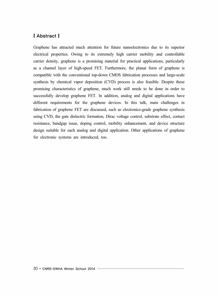
AbstractGraphene has attracted much attention for future nanoelectronics due to its superior electrical properties. Owing to its extremely high carrier mobility and controllable carrier density, graphene is a promising material for practical applications, particularly as a channel layer of high-speed FET. Furthermore, the planar form of graphene is compatible with the conventional top-down CMOS fabrication processes and large-scale synthesis by chemical vapor deposition (CVD) process is also feasible. Despite these promising characteristics of graphene, much work still needs to be done in order to successfully develop graphene FET. In addition, analog and digital applications have different requirements for the graphene devices. In this talk, main challenges in fabrication of graphene FET are discussed, such as electronics-grade graphene synthesis using CVD, the gate dielectric formation, Dirac voltage control, substrate effect, contact resistance, bandgap issue, doping control, mobility enhancement, and device structure design suitable for each analog and digital application. Other applications of graphene for electronic systems are introduced, too.

CNRS-EWHA Winter School 2014 • 31
[OOE-4]
Optical Properties and Application of borondifluoride
complexes.
Dr Anthony D’Aléo[Affiliation] Aix Marseille University
Centre Interdisciplinaire de Nanoscience de Marseille (CINaM-UMR 7325)[Contact] 163 Avenue de Luminy-Case 913-13288-Marseille Cedex 9-France
[Tel] +33-(0)6 17 24 80 84[Fax] +33-(0)4 91 41 89 16
[Email] [email protected]
Curriculum Vitae[Education]
2006 Ph.D., University of Amsterdam (The Netherland) 2002 M.S., University of Bordeaux (France) 2000 B.S., University of Bordeaux (France)
[Positions]
2009.10~present CNRS researcher (CINaM, Marseille, France) 2007.09~2009.10 Postdoctoral researcher, University of California, Berkeley (USA) 2006.02~2007.08 Postdoctoral researcher, ENS Lyon (France)
[Research Interests]
Organic Optoelectronics, Photophysics and Non linear Optics

32 • CNRS-EWHA Winter School 2014
Abstract2’-Hydroxychalcone and curcuminoid derivatives are naturally occurring dyes. Coordination of those chromophores with borondifluoride leads to fluorescent compounds in solution and in solid state. Upon appending strong donor end-groups, we have succeeded in shifting the visible electronic absorption to the red with an emission that can reach the near infrared (NIR) for some compounds. Furthermore, the introduction of polycyclic aromatic hydrocarbons or linear conjugated groups at the meso position of the curcuminoid backbone strongly influences ground- and excited-states properties. The photophysical properties of a series of dyes will be presented in solution and in the solid state, together with a structure-photophysical relationship study. In addition, application of those molecules toward imaging will be shown.

CNRS-EWHA Winter School 2014 • 33
[OOE-5]
Ultrafast photo-physics of organic nanostructures:
New Materials for organic solar cells
Prof. Stefan Haacke
[Affiliation] Strasbourg University - CNRS
Institute for Physics and Chemistry of Materials (IPCMS)
[Contact] 23, rue du Loess; F-67034 Strasbourg Cedex
[Tel] +33-3-88 10 71 71
[Email] [email protected]
Curriculum Vitae[Education]
1994 Ph.D., Université Joseph Fourier Grenoble (France) 1990 M.S., Technical University Berlin (Germany)
[Positions]
Since 2004 Professor in Physics, University of Strasbourg 1999~2004 Assistant Professor Physics Department Lausanne University & EPFL 1994~1999 Res. Associate Inst. Micro-&Optoelectronics, École
Polytechnique Fédérale de Lausanne 1990~1994 PhD student in Physics, High Magnetic Field Lab Grenoble,
University J. Fourier Grenoble
[Research Interests]
Ultrafast photo-induced processes in photo-active proteins, biomolecules and organic functional nanostructures, instrumentation for ultrafast spectroscopy

34 • CNRS-EWHA Winter School 2014
AbstractSolar cells using liquid crystal (LC) films of donor-acceptor (DA) molecules are a new approach, in which the ratio of DA interface-to-volume is maximized, leading to fairly good performances [2]. The motivation is to make the distance to the D-A interface shorter than the exciton diffusion length (typically 10 nm). We have studied LC films of bisthiophene-derivatives forming D and perylenendiimide as A, by femtosecond transient absorption (TA) spectroscopy. Due to the strong electronic coupling between D's the initial laser excitation, selectively tuned in the absorption of D, excites a coherent superposition of many D molecules (exciton) that decays within 60 fs into a charge transfer (CT) state, that localizes on a slower 0.4 ps time scale [3]. We will present results obtained for a new type of donor family incorporated in the DA's that incorporate moieties with different electron-donating and -deficient character, thereby offering a handle to control the localization of HOMO and LUMO orbitals. A smectic liquid crystal state is formed at room temperature. CT lifetimes larger than 2 ns are now observed and the results are rationalized within the Marcus theory for charge transfer.
[1] Heliatek press release, http://www.heliatek.com/newscenter/latest_news/, January 16, 2013
[2] L. Bu and al., J. Am. Chem. Soc., 2009, 131, 13242-13243[3] T. Roland and al., Phys. Chem. Chem. Phys, 2012, 14, 273-279

CNRS-EWHA Winter School 2014 • 35
[OOE-6]
High efficiency organic light-emitting diodes using
delayed fluorescence
Prof. Chihaya Adachi
[Affiliation] Kyushu UniversityCenter for Organic Photonics and Electronics Research (OPERA)
[Contact] 744 Motooka, Nishi, Fukuoka 819-0395[Tel] +81-92-802-6923[Fax] +81-92-802-6921
[Email] [email protected]
Curriculum Vitae[Education]
1991 D. Eng. Materials Science and Technology, Kyushu University (Japan)
1988 M. Eng. Materials Science and Technology, Kyushu University (Japan)
[Positions]
1991~ Ricoh Co., Chemical Products R&D Center, Research Chemist and Physicist(Japan)
1996~ Shinshu University, Department of Functional Polymer Science, Research Associate (Japan)
1999~ Princeton University, Department of Electrical Engineering, Research Staff (USA)
2001~ Chitose Institute of Science and Technology, Associate Professor (Japan)
2004~ Chitose Institute of Science and Technology, Professor (Japan) 2006~ Kyushu University, Center for Future Chemistry (Japan)

36 • CNRS-EWHA Winter School 2014
2010~ Kyushu University, Center for Organic Photonics and Electronics Research (OPERA) (Japan)
[Research Interests]
Organic Electronics, Properties and physics of Organic semiconducting devices, Organic photo-physics and chemistry
AbstractFluorescence-based organic light-emitting diodes (OLEDs) attract much attention because of their long operational lifetimes, high color purity of EL, and potential to be manufactured at low-cost in next generation full-color display and lighting applications. While the exciton production efficiency is limited to 25% due to the deactivation of triplet excitons in fluorescence based OLEDs, we report high efficiency OLEDs demonstrating external quantum efficiencies nearly 20%. The high performance was enabled by utilization of thermally activated delayed fluorescence molecules as assistant dopants that permit efficient transfer of all electrically generated singlet and triplet excitons from the assistant dopants to the fluorescent emitters.

CNRS-EWHA Winter School 2014 • 37
[OOE-7]
Thermally-Assisted Delayed Fluorescence Mediated
by Excited-State Proton Transfer
Prof. Soo Young Park
[Affiliation] Seoul National UniversityCenter for Supramolecular Optoelectronic Materials (CSOM)[Contact] 1 Gwanak-ro, Kwanak-gu, Seoul 151-744, Korea
[Tel] +82-2-880-8327[Fax] +82-2-885-1748
[Email] [email protected]
Curriculum Vitae[Education]
1988 Ph.D., Seoul National University (Korea) 1982 M.S., Seoul National University (Korea) 1980 B.S., Seoul National University (Korea)
[Positions]
1995~present Professor, Seoul National University 1985~1995 Researcher, Korea Inst. Sci. Tech. (KIST) 2010~ Fellow, Korean Academy of Science and Technology (KAST)
[Research Interests]
Organic Semiconductors: Luminescent Molecule, Supramolecule, and Macromolecule

38 • CNRS-EWHA Winter School 2014
AbstractFluorescent molecules which harness excited-state intramolecular proton transfer (ESIPT) process have been noted for their special and unique photophysical properties. Exploiting the four-level nature of photoluminescence process which is mediated by the reversible proton transfer, we ha demonstrated novel class of ESIPT molecules which show innovative photoelectronic applications like lasing, sensing, and molecular pixel behaviors. In particular, we could observe a thermally-assisted delayed fluorescence (TADF) emission in the proton transferred ESIPT tautomer, which may promise applications in OLED devices. To fully understand the mechanism of TADF process associated with ESIPT process, we have designed and synthesized a series of azole-based ESIPT molecules. Details of their photophysical properties and the possible mechanism of TADF will be discussed in this presentation.

CNRS-EWHA Winter School 2014 • 39
[SMF-1]
Molecular Spintronics
Dr. Sergio Tatay Aguilar
[Affiliation] Instituto de Ciencia Molecular (ICMol), University of Valencia,
Spain & Unité Mixte de Physique CNRS/Thales, France
[Contact] C. Catedrático José Beltrán 2, 46980 Paterna (SPAIN)
[Tel] +34-96-354-44-05
[Email] [email protected]
Curriculum Vitae[Education]
2009/12 Postdoc, Unité Mixte de Physique CNRS/Thales (France) 2004/08 Ph.D., University of Valencia (Spain) 2003 M.Sc., University of Valencia (Spain)
[Positions]
Research scientist, University of Valencia (SPAIN)
[Research Interests]
Organic/Molecular Electronics and Spintronics, Surface Science, Chemical Synthesis

40 • CNRS-EWHA Winter School 2014
AbstractVery recently, molecular spintronics, a rising research field at the frontier between organic chemistry and spintronics, has opened novel and exciting opportunities in terms of functionalities and performances for spintronics devices. Beyond, plasticity and low cost, carbon based materials such as graphene and nanotubes were first seen as very promising for spintronics devices due to their expected long spin lifetime and potential for becoming the ultimate spintronics media. It was only very recently that new spintronics tailoring opportunities that could be brought by molecules and molecular engineering were unveiled. We will present experimental results unveiling promising uses of carbon based molecules for spintronics.The molecular structure, the local geometry at the molecule-electrode interface and more importantly the ferromagnetic metal/molecule hybridization can strongly influence interfacial spin properties going from spin polarization enhancement to its sign control in spintronics devices [2]. We will show successful spin dependent transport measurements at room temperature and high bias on ferromagnet/molecules/ferromagnet magnetic tunnel junctions, where molecules are organic semiconductors (Alq3) or self-assembled monolayers (SAMs) [3]. We will also highlighting the crucial role of the interface and introduce inelastic electron tunnel spectroscopy (IETS) as a valuable tool to directly control the presence of the molecules inside the junction.

CNRS-EWHA Winter School 2014 • 41
[SMF-2]
Electronic ferroelectricity and multiferroic domains in
LuFe2O4 observed by scanning probe microscopy
Prof. Yoon H. Jeong
[Affiliation] Dept of Physics, POSTECH
[Contact] Cheongam-Ro 77, Pohang, Korea
[Tel] +82-54-279-2078
[Fax] +82-54-279-3099
[Email] [email protected]
Curriculum Vitae[Education]
1987 Ph.D., Univ of Chicago
[Positions]
2010.01~2012.12 Chair of Physics Department and Dean of Natural Sciences, POSTECH
2009.03~2009.12 Director of Math and Physical Sciences Division, National Research Foundation
2000.07~2009.02 Director of Electron Spin Science Center, POSTECH 1988.06~ Professor at POSTECH, Korea
[Research Interests]
Materials: quantum functional materials, electrical steelsMeasurement methods: thermal analysis, calorimetry, X-ray scattering and absorption
using SR, domain observation by SPM

42 • CNRS-EWHA Winter School 2014
AbstractLuFe2O4 is a multiferroic system which exhibits ferroelectricity, charge order, and ferrimagnetic order simultaneously below ~230 K. The ferroelectric domains of LuFe2O4
are imaged with both piezoresponse force microscopy (PFM) and electrostatic force microscopy (EFM), while the magnetic domains are characterized by magnetic force microscopy (MFM). Comparison of PFM and EFM results lead to a conclusion that the ferroelectricity is of electronic origin as opposed to the usual displacive one. Simultaneous characterization of ferroelectric and magnetic domains by EFM and MFM, respectively, on the same surface of LuFe2O4 reveals that both domains have irregular patterns of similar shape, but the length scales are different. The linear dimension is approximately 100 nm and 200 nm for ferroelectric and magnetic domains, respectively. We also demonstrate that the origin of the formation of irregular domains in LuFe2O4
is not extrinsic but intrinsic.

CNRS-EWHA Winter School 2014 • 43
[SMF-3]
Latest developments in the quest for room
temperature multiferroic thin films
Prof. Nathalie Viart
[Affiliation] Institut de Physique et Chimie des Matériaux de StrasbourgCNRS-Université de Strasbourg
[Contact] 23 rue du Lœss BP43, 67034 Strasbourg, France[Tel] +33 3 88 10 71 29[Fax] +33 3 88 10 72 47[Email] [email protected]
Curriculum Vitae[Education]
1996 Ph.D., University of Strasbourg (France) 1993 M.S., University of Strasbourg (France)
[Positions]
Since 2007 Full Professor, University of Strasbourg (France) 1997 Assistant Professor, University of Strasbourg (France) 1996-97 Postdoctoral researcher, University of Oxford (UK)
[Research Interests]
Functional oxides thin films, Multiferroics, Magnetoelectrics

44 • CNRS-EWHA Winter School 2014
AbstractThe development of multiferroic or magnetoelectric materials based devices is hindered by the cruel lack of such materials exhibiting room temperature properties. A serious candidate lies in the orthorhombic gallium ferrite, Ga2-xFexO3, for it is pyroelectric, magnetoelectric and ferrimagnetic with a Néel temperature above room temperature for x>1.3. We have initiated a research program which aims at fully investigating the possibilities offered by this family of compounds. Our researches concern both bulk polycrystalline samples and thin films. I will present our latest results concerning the magnetic and electric properties of both kind of samples, in relation with their structure, and lay a stress on the various original investigation methods developed for these studies.The magnetoelectric effect we have evidenced in the films, associated with a Néel temperature above room temperature and a net magnetization at room temperature, could open real perspectives for single-phased magnetoelectric materials applications.

CNRS-EWHA Winter School 2014 • 45
[HMF-1]
Hybrid metal nanoparticles for bioimaging and
optical protection
Prof. Stephane Parola
[Affiliation] Laboratoire de Chimie ENS Lyon
[Contact] 46 allée d’Italie, 69364 Lyon, France
[Tel] +33 472 72 81 57
[Email] [email protected]
Curriculum Vitae[Education]
2004 Habilitation à Diriger des Recherches, University Lyon 1 (France) 1996 European Ph.D., University of Nice Sophia-Antipolis (France) 1992 M.S., University of Nice Sophia-Antipolis (France)
[Positions]
Since 2010 Animator of the Group Functional Materials and Photonics, Chemistry Lab., Ecole Normale Supérieure de Lyon (France).
Since 2005 Professor, University Lyon 1 (France) 1997~2004 Assistant Professor, University Lyon 1 (France) 1996~1997 Assistant professor, University of Nice Sophia-Antipolis (France) 1992~1995 Research scientist, Chalmers University of Technology (Sweden)
[Research Interests]
Molecular precursors, chemistry of materials, colloidal chemistry, sol-gel science, nanomaterials, plasmonics, photonics.

46 • CNRS-EWHA Winter School 2014
AbstractThe development of new hybrid nanoplatforms which can combine optical properties of chromophores with inorganic nanomaterials is of increasing interest for optical and biomedical purposes. In the last decade, noble metal nanoparticles have sparked wide interest for developing new optical applications in the context of bio-imaging, photo-thermal therapy, optical sensors and solar cells. This interest is essentially due to their unique optical properties related to their Localized Surface Plasmon Resonances (LSPR). This optical property at the nanoscale has been used to enhance the optical properties of molecular systems located close to noble metal nanostructures as, for instance, in SERS experiments. Numerous works are investigating the possibility of using the light interaction with metallic nanoparticles to improve the luminescence of chromophores. These nanoparticles can be used for bioimaging or phototherapy. Combination of metal nanoparticles and chromophores in composite materials (films, monoliths) is also a great challenge for optical applications but requires control of dispersion during the process in order to control molecule to particles interactions. It was successfully achieved and showed strong impact of the metal-molecule interactions on the overall optical properties. This will be illustrated by examples of applications in fluorescence imaging, dark field imaging, photodynamic therapy on cells and optical protection against lasers.

CNRS-EWHA Winter School 2014 • 47
[HMF-2]
Halogen bonding in molecular solids: control of
charge transfer
Dr. Marc Fourmigué[Affiliation] Université de Rennes & CNRS
Institut des Sciences Chimiques de Rennes (ISCR)[Contact] Campus de Beaulieu, 35042 RENES (France)
[Tel] +33-223235243[Fax] +33-223236732
[Email] [email protected]
Curriculum Vitae[Education]
1997 Habilitation, University Nantes (France) 1988 Ph.D., University Paris-Sud (Orsay, France), with University
Copenhagen (DK) 1985 M.S. (DEA Matériaux Paris VI) & Chemistry Engineer ESPCI (Paris,
France)
[Positions]
2006.01~present Research scientist, MaCSE group at ISCR (Rennes, France) 2002.01~2005.12 Research scientist, Université Angers (France) 1995.01~2001.12 Research scientist, Institut des Matériaux de Nantes (France) 1994.07~1994.12 Postdoctoral researcher, UCSB (Santa Barbara, USA) 1990.10~1994.06 Jr. Research scientist, Physique des Solides (Orsay, France) 1988.09~1990.09 Postdoctoral researcher, Physique des Solides (Orsay, France)
[Research Interests]
Molecular Conductors, Organic Solid State, Intermolecular Interactions, Crystallography

48 • CNRS-EWHA Winter School 2014
AbstractHalogen bonding interactions take place between the so-called hole of activated organic halogens and Lewis bases. The directionality of this interaction allows for its use in crystal engineering strategies. In this lecture, I will illustrate the involvement of such halogen bonding interactions in the elaboration of supramolecular porous architectures around halide anions as Lewis bases. Its electrostatic character will be demonstrated from its evolution in organic charge transfer salts with variable ionicity. Interaction of radical, iodinated tetrathiafulvalenes with low symmetry counter ions (chiral sulfonates, non-centrosymmetric perchlorate) allows for the isolation of original chiral conductors and bilayer systems.

CNRS-EWHA Winter School 2014 • 49
[HMF-3]
Design of nanoparticles of new and complex
morphology for assembly purpose
Prof. Etienne Duguet
[Affiliation] University of BordeauxBordeaux Institute of Condensed Matter Chemistry (ICMCB-CNRS)[Contact] 87 ave du Dr Albert Schweitzer, F-33608 Pessac, France
[Tel] +33-540-002-651[Fax] +33-540-002-761
[Email] [email protected]
Curriculum Vitae[Education]
2000 Accreditation to supervise research in Materials Chemistry 1992 Ph.D. in Polymer Chemistry, University of Bordeaux (France) 1988 Engineering degree in Physical Chemistry of the Ecole Nationale
Supérieure de Chimie et Physique de Bordeaux (France)
[Positions]
2011.04~present Managing Director of the Cluster of Excellence AMADEus 2010.01~present Deputy Director of ICMCB-CNRS 2002.09~present Group leader at ICMCB-CNRS 1992.09~present Assistant-professor, then full professor in Materials Chemistry at
the University of Bordeaux, posting to ICMCB-CNRS
[Research Interests]
Hybrid organic-inorganic nanomaterials: nanoparticle synthesis, surface functionalization, encapsulation in macromolecular corona or shell made of polymer or silica, self- assembly; Janus particles, patchy particles, colloidal molecules; Application in optics: pigments, photonic crystals, metamaterials
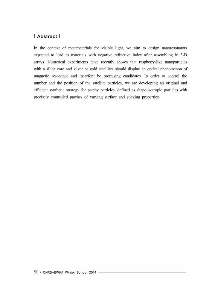
50 • CNRS-EWHA Winter School 2014
AbstractIn the context of metamaterials for visible light, we aim to design nanoresonators expected to lead to materials with negative refractive index after assembling in 3-D arrays. Numerical experiments have recently shown that raspberry-like nanoparticles with a silica core and silver or gold satellites should display an optical phenomenon of magnetic resonance and therefore be promising candidates. In order to control the number and the position of the satellite particles, we are developing an original and efficient synthetic strategy for patchy particles, defined as shape-isotropic particles with precisely controlled patches of varying surface and sticking properties.

CNRS-EWHA Winter School 2014 • 51
[CS-1]
Self-assembly of organic molecules on
semiconductor surfaces
Prof. Fabrizio CLERI
[Affiliation] University of Lille IInstitute of Electronics, Microelectronics and Nanotechnology (IEMN Cnrs Umr 8520)
[Contact] Av. Poincaré BP 60069, 59652 Villeneuve d’Ascq (France)[Tel] +33-320-197928[Fax] +33-320-197884
[Email] [email protected]
Curriculum Vitae[Education]
2004 HDR, Louis Pasteur University of Strasbourg (France) 1985 Doctor in Physics, University of Perugia (Italy)
[Positions]
2010~present Director of the Master School in Biophysics and Medical Physics, University of Lille I (France)
2006~present Full professor in Physics, University of Lille (France), and Group leader, IEMN Cnrs, Lille (France)
1992~2005 Senior scientist, Group leader, ENEA (Italy) 1985~1992 Staff Scientist, ENEA (Italy)Visiting professor, ISS University of Tokyo (Japan) (09-12/2008)Visiting professor, Rensselaer Polytechnic Troy, New York (USA) (01-04/2003) Visiting scholar, University of Chicago, Argonne National Laboratory (USA)
(06/1995~06/1998)

52 • CNRS-EWHA Winter School 2014
Visiting scientist, MIT Cambridge (USA) (06/1994 – 12/1994) Associate Editor of Applied Physics Letters, and European Physical Journal B
(Condensed Matter and Complex Systems)
[Research Interests]
Statistical mechanics of nanostructured and disordered materials; Biophysics and Nano-Bio interfaces; Multi-scale computer simulation of atomic and molecular systems
AbstractHigh-density packing in organic crystal is usually associated with an increase of the coordination between molecules, since the early formulations of molecular symmetry arguments by Kitaigorodski in the late 50s. We contend the validity of this concept for two-dimensional molecular networks self-assembled on solid semiconductor surfaces, by using a combination of scanning tunneling microscopy experiments and multi-scale computer simulations. We study the phase transitions between different polymorphs and we demonstrate that, contrary to simple intuition, the structure with the lowest packing density may correspond indeed to the highest coordination. The subtle competition between intermolecular and surface dispersion forces (often ignored in the discussions about molecular symmetry) is at the origin of such a counter-intuitive result. Having the lowest free energy, such low-density structures spread out macroscopically as the most stable polymorphs over a wide range of molecular concentrations.

CNRS-EWHA Winter School 2014 • 53
[CS-2]
First-principles calculation of effects of magnetic
impurities on topological surface states
Prof. Hyoung Joon Choi
[Affiliation] Yonsei UniversityDepartment of Physics
[Contact] 50 Yonsei-ro, Seodaemun-gu, Seoul 120-749, Korea[Tel] +82-2-2123-2608[Fax] +82-2-392-1592
[Email] [email protected]
Curriculum Vitae[Education]
2000 Ph.D., Seoul National University (Korea) 1994 M.S., Seoul National University (Korea) 1992 B.S., Seoul National University (Korea)
[Positions]
2005~present Professor, Yonsei University (Korea) 2003~2005 Professor, Korea Institute for Advanced Study (Korea) 2000~2003 Miller Research Fellow, University of California, Berkeley (USA)
[Research Interests]
Density Functional Theory, Electronic Structures, Magnetism, Superconductivity, Transport

54 • CNRS-EWHA Winter School 2014
AbstractWe study effects of magnetic impurities on topological surface state of Sb (111) and Bi2Se3 (111) surfaces by using first-principles density-functional method. The spin-orbit interaction is implemented into the SIESTA code in a form of additional fully non-local projectors, and supercells are used to calculate surface band structures. We consider Fe and Mn impurities at interstitial sites and substitutional sites near the surface. To analyze effects of impurities on the topological surface states, we simulate ARPES spectra and obtain projected density of states of impurities near the Fermi level. We find that Fe and Mn impurities have significant local magnetic moments near the Sb surface, and their effects on the dispersion of the surface states depend strongly on the impurity sites. We discuss scattering mechanism of the surface states by the impurities and its implication on the ordering of impurity magnetic moments. This work was supported by NRF of KOREA (Grant No. 2011-0018306) and KISTI supercomputing center (Project No. KSC-2013-C3-062).

CNRS-EWHA Winter School 2014 • 55
[CS-3]
Improved design of metal-organic frameworks for
efficient gas adsorption by multi-scale simulation
with strong accuracy
Dr. Sang Soo Han
[Affiliation] Korea Institute of Science and Technology (KIST)Center for Computational Science
[Contact] Hwarangno 14-gil 5, Seongbuk-gu, Seoul 136-791, Republic of Korea[Tel] +82-2-958-5441[Fax] +82-2-958-5451
[Email] [email protected]
Curriculum Vitae[Education]
2005 Ph.D., Korea Advanced Institute of Science and Technology (Rep. of Korea)
2001 M.S., Hanyang University (Rep. of Korea) 1999 B.S., Hanyang University (Rep. of Korea)
[Positions]
22013.06~present Senior research scientist, KIST (Rep. of Korea) 2009.02~2013.05 Senior research scientist, KRISS (Rep. of Korea) 2005.10~2009.01 Postdoctoral researcher, California Institute of Technology (USA) 2005.03~2005.10 Postdoctoral researcher, KAIST (Rep. of Korea)
[Research Interests]
Design of novel energy-related materials (porous materials, batteries, and catalysts) by multi-scale simulation

56 • CNRS-EWHA Winter School 2014
AbstractRecently microporous crystalline metal-organic frameworks (MOFs), which are
composed of metallic joints and organic struts, represent exceptional porosity (up to 90%) and high surface area (up to 10,000 m2/g), which stimulated many studies to investigate the utility for using these materials as gas adsorbents for hydrogen (H2), methane (CH4), and carbon dioxide (CO2) storage. In this talk, I will introduce how to accurately predict isotherms of the gases in the MOFs by a multi-scale simulation scheme including first principles calculation, Monte-Carlo simulation, and molecular dynamics simulation with reactive force field. And then, I will discuss several strategies for improving gas adsorption amount in the porous materials
CNRS-EWHA Winter School 2014 • 57
[CS-4]
Origins of anomalous water permeation through
graphene oxide membrane
Prof. Young-Woo Son
[Affiliation] Korea Institute for Advanced Study
[Contact] KIAS Hoegiro 85, Dongdaemun-Gu, Seoul, Korea
[Tel] +81-92-802-6923
[Email] [email protected]
Curriculum Vitae[Education]
2004 Ph.D., Seoul National University 2000 M.S., Seoul National University 1997 B.S., Seoul National University
[Positions]
2008.09~present Professor, KIAS 2007~2008.08 Assistant Professor, Konkuk University 2004~2007 Postdoctor, UC Berkeley
[Research Interests]
Condensed matter theory

58 • CNRS-EWHA Winter School 2014
AbstractWater flows and its structures inside the low dimensional materials have been considered seriously owing to their fundamental and practical importances. Recently, the anomalous perfect penetration of water through graphene oxide membrane was demonstrated although the membrane was impenetrable for other liquids and even gases. The unusual auxetic behavior of graphene oxide in the presence of water was also reported. Here, based on first-principles calculations, we establish atomistic models for hybrid systems composed of water and graphene oxides revealing the anomalous water behavior inside the stacked graphene oxides. We show that formation of hexagonal ice bilayer in between the flakes as well as melting transition of ice at the edges of flakes are crucial to realize the unimpeded water permeation across the stacked structures. The interlayer distance that can be controlled either by oxygen reduction process or pressure is shown to determine the water flow thus highlighting a unique water dynamics in randomly connected two-dimensional spaces.

CNRS-EWHA Winter School 2014 • 59
[CS-5]
Structural changes in amorphous GexSe1-x under
the effect of pressure by first principles molecular
dynamics
Assil Bouzid
[Affiliation] Institut de Physique et de Chimie des Matériaux de Strasbourg (IPCMS)
[Contact] 23 rue du Loess, BP 43, F-67034 Strasbourg Cedex 2, France [Tel] +33-388107143 [Fax] +33-388107250
[Email] [email protected]
Curriculum Vitae[Education]
2011~present Ph.D., University of Strasbourg (France) (defense October 3, 2014)
2010~2011 Master’s degree on condensed matter and nanophysics, Univ of Strasbourg (France)
2009~2011 Master’s degree on quantum physics, University of Tunis El Manar (Tunisia)
2005~2009 “Maîtrise” (Bac+4) degree on fundamental physics, University of Monastir (Tunisia)
[Research Interests]
Atomic scale modeling of materials, amorphous chalcogenides, phase change materials

60 • CNRS-EWHA Winter School 2014
AbstractThe structural changes in the prototypical network-forming glasses GeSe2 and GeSe4 were investigated at pressures up to~15 GPa by using first-principles molecular dynamics. The results are compared to recent neutron diffraction data by the team of Prof. P. S. Salmon. The structural transformation undergone by the GeSe2 network is found to be substantially different from those observed in oxide glasses such as SiO2 and GeO2[1-2]. The densification of amorphous GeSe2 occurs in two steps. For pressures lower than 8.5 GPa, edge-sharing tetrahedra persist as the dominant structural motif and the chemical order is preserved. When increasing the pressures for values higher than 8.5GPa, a conversion from edge-sharing to corner-sharing configurations takes place in conjunction with a steady increase of the mean coordination number. At the transition pressure, most of the higher coordinated Ge-centered polyhedral contain homopolar bonds. Therefore, the homopolar bonds play a mediating role in the occurrence of the transition. This mechanism of network collapse is likely to be generic for the class of glass-forming materials where homopolar bonds and edge-sharing motifs are prevalent in the ambient pressure network [3]. In the case of GeSe4, no structural change has been recorded. In agreement with the experiment [4], the ambient pressure network and the chemical order are preserved upon compression. This behavior is due to the Se chains. By twisting and reducing the Se-Se-Se internal bond angles, Se chains fill the inter-tetrahedral cavities and prevent the system from undergoing any structural transition when high pressures are applied.
References:[1] A. C. Wright, J. Non-Cryst. Solids 179, 84 (1994).[2] P. S. Salmon, A. C. Barnes, R. A. Martin, and G. J. Cuello, J. Phys.: Condens.
Matter 19, 415110 (2007).[3] Kamil Wezka, Assil Bouzid and Co. To be published[4] L. B. Skinner et al. J. Phys. Chem. C, 116 (3), pp 2212–2217 (2012).

CNRS-EWHA Winter School 2014 • 61
[HMF-4]
New electroactive tetrazines; Electrochemistry
fluorescence and applications.
Prof. Pierre Audebert
[Affiliation] Ecole Normale Supérieure de CachanPhotophysique et Photochimie Molécualire et Supramoléculaire (PPSM)
[Contact] 61 Av du Président Wilson, 94230 CACHAN France[Tel] +33-1-47405313.[Fax] +33-1-47402454.
[Email] [email protected]
Curriculum Vitae[Education]
1982 Engineer ESPCI Paris 1987 PhD, U. Joseph Fourier, Grenoble.
[Positions]
1998~present Professor, Group leader in PPSM, ENS Cachan (near Paris, France)
1993~1998 Professor, Group leader in University of Franche Comté, Besançon, (France)
1988~1993 CNRS Research scientist, University of Paris 7 (France)
[Research Interests]
Molecular electrochemistry, Conducting Polymers, Sol-gel Chemistry, Organic Optoelectronics, Electrofluorochromism, Tetrazines.

62 • CNRS-EWHA Winter School 2014
AbstractThe tetrazine ring is the most electron deficient aromatic ring in the CHON
chemistry, and in particular in some cases displays a n-* transition which gives rise to a particular fluorescence with especially long decay times because of the forbidden character of the transition1. Its electron deficient character also allows the tetrazine ring to be reversibly reduced electrochemically, and thus opens the route towards many applications like the fabrication of electron transferring polymers or n-dopable conducting polymers.
Another interesting feature, tetrazines bearing electron-withdrawing enough groups are also fluorescent, and also have a very high potential in the excited state, which can be the basis for fluorescence sensors or photocatalysis. Conversion to the anion-radical suppresses the fluorescent character, which makes them ideal candidates for the electrochemical switching of fluorescence, usually called electrofluorochromism2.
We will also describe the synthesis and the electrochemistry of new tetrazines bearing UV antennas that display brilliant yellow fluorescence under UV illumination (see above), a unique feature among organic fluorophores. A new and unique commercial application, the LumicyanoR for the fluorescent revelation of fingerprints, will be presented.
1 G. CLAVIER and P. AUDEBERT “s-Tetrazines as building blocks for new functional molecules and molecular materials”, Chem. Rev., 2010, 110, 3299-3314.
2 P. AUDEBERT and F. MIOMANDRE, Electrofluorochromism: from molecular systems to set-up and display. Chem. Science, 2013, 4, 575.

CNRS-EWHA Winter School 2014 • 63
[HMF-5]
Electrochemistry as a Tool for Making Controlled
Surface Functionalizations.
Dr. Philippe Hapiot
[Affiliation] CNRS – University of RennesInstitute of Chemical Sciences of Rennes (MaCSE team)[Contact] Campus de Beaulieu – 35042 Rennes - France
[Tel] +33-2-23-23-5939[Fax] +33-2-23-23-6732
[Email] [email protected]
Curriculum Vitae[Education]
1985 Ph.D., University of Paris 7 (France)
[Positions]
2000.04~present “Directeur de Recherche CNRS” – University of Rennes 1.
[Research Interests]
Electrochemistry: Electron transfer and Redox chemistry; Surface functionalization.

64 • CNRS-EWHA Winter School 2014
AbstractSurfaces functionalization presents growing interests due to the large range of possible applications as for example those in analytical, bio-analytical chemistry or molecular electronic. In relation with these expending fields, classical electrochemistry and the more recent developments of electrochemistry at a local scale (micro- and nano-electrochemistry) appear as versatile and straightforward means for building and analyzing functionalized and nanostructured surfaces.In this lecture, we will discuss how the surface reaction properties of a functionalized surface on different common substrates (Si, C, Pt, Au,…) could be probed through adapted and relatively low cost electrochemical techniques, Scanning Electrochemical Microscopy (SECM) being particularly well adapted. SECM also permits reversible or irreversible patterning of the layer. Different examples of such modified surfaces and of their applications will be presented, notably recent results in relation with the study of surface reactions implying reactive oxygen species or « click » chemistry coupling.

CNRS-EWHA Winter School 2014 • 65
[HMF-6]
Tracking structure and dynamics of biological
systems by two-dimensional optical spectroscopy
Dr. Ivan Rivalta
[Affiliation] CNRSLaboratoire de Chimie, École Normale Supérieure de Lyon
[Contact] 46, allée d'Italie 69364 Lyon, France[Tel] +334-72-72-8843[Fax] +334-72-72-8860
[Email] [email protected]
Curriculum Vitae[Education]
2007 Ph.D., Università della Calabria (Italy) 2003 M.S., Università della Calabria (Italy)
[Positions]
2014.01~present Chargé de Recherche at ENS-Lyon (France) 2012.04~2013.12 Research scientist, Università di Bologna (Italy) 2010.04~2012.04 Research scientist, Yale University (USA) 2009.04~2010.04 Postdoctoral researcher, ETH Zurich (UK) 2007.04~2009.04 Postdoctoral researcher, Università della Calabria (Italy)
[Research Interests]
Theoretical Spectroscopy, Protein Dynamics, Chemical Reactivity and Catalysis

66 • CNRS-EWHA Winter School 2014
AbstractTwo-dimensional electronic spectroscopy (2DES) based on ultrashort laser pulses is a cutting-edge technique to track electronic transitions in complex systems with unprecedented spectral and time resolution. 2DES can be used to investigate a wide range of systems in physical chemistry, energy sciences and biophysics, providing a wealth of novel information on molecular structure and dynamics with respect to traditional 1D experiments. However, the interpretation of 2D electronic spectra is challenging and computational modeling is required. In this talk a computational tool that can be routinely applied to accurately simulate 2DES spectra of multichromophoric systems is introduced. Ab-initio methods have been used to reliably calculate the electronic properties within a hybrid QM/MM scheme in conjunction with molecular dynamics techniques to assess environmental and conformational effects that shape the 2D electronic spectra. Applications to protein folding dynamics and retinal photochemistry are showed.

CNRS-EWHA Winter School 2014 • 67
[HMF-7]
Hybrid interfaces in layered systems: chemistry and
functionality
Dr. Pierre Rabu
[Affiliation] IPCMS, UMR7504 CNRS-Université de Strasbourg and NIE
[Contact] 23, rue du Loess, BP43 67034 Strasbourg cedex 2, France.
[Tel] +33-(0)3-88107135
[Fax] +33-(0)3-88107147
[Email] [email protected]
Curriculum Vitae[Education]
1999 Habilitation, Université Louis Pasteur, Strasbourg, France 1990 PhD, University of Nantes, France 1987 DEA, ENSM, University of Nantes, France 1986 MSc.&T., University of Nantes, France 1984 DEUG A, University of Nantes, France
[Positions]
2014-03~ Head of the Department of Inorganic Chemistry of Materials of IPCMS
2005~ Research director, IPCMS, CNRS-UNISTRA, Strasbourg France. 2005~2008 Director of the national research group GDR 2922 CNRS
“Multifunctional Hybrid Materials”. 1990~2005 Researcher, IPCMS, UMR7504 CNRS-ULP, Strasbourg France 1989~1990 Graduate assistant, Dept. of Chemistry, Univ. of Nantes, CIES
Rennes.

68 • CNRS-EWHA Winter School 2014
[Research Interests]
Hybrid organic-inorganic materials, Solid state chemistry, Molecular magnetism, Layered materials
AbstractThe purpose of this lecture is to present our results concerning the synthesis via chemical routes of new functional materials based on the hybrid organic-inorganic approach. This approach means to assemble nanometer-sized bricks or components of different nature, controlled at the molecular level to elaborate new functional (hetero-) structures. Examples will be presented to evaluate such methodology as a route to new materials with user defined and possibly coupled properties, as magnetism or optical properties. We will particularly focus on the interfaces between components and their influence on the dimensionality and properties of post-modified layered transition metal based compounds.

Abstracts for poster presentation
Poster Session : June 25 (Wed)Poster 1 ~ Poster 34

Abstracts for poster presentation • 71
Poster-1
Semiconductor Epsilon-Near-Zero Nano-Optics
Young Chul Jun
Department of Physics, Inha University, Republic of Korea
Epsilon-near-zero (ENZ) materials have attracted attention for their highly unusual and intriguing optical properties. For example, ENZ materials were employed for perfect coupling through a narrow channel, optical switching and bistability, and directivity control of antennas. More recently, it was also pointed out that a thin ENZ layer supports a new type of guided modes near the epsilon zero frequency, termed ENZ modes. Here, we present our recent work on ENZ nano-optics based on ultra-thin, doped semiconductors: (i) Novel strong coupling between planar metamaterials and ENZ modes, (ii) Narrowband thermal emission from an ENZ material, (iii) Perfect absorption in an ENZ material.

72 • CNRS-EWHA Winter School 2014
Poster-2
Topological surface states in Bi2Te3 nanowires and
nanotubes
Byung Cheol Park*, Nalae Han*, Ha-Yeong Kim**, Sung-Jin Kim**, Kyung Hwa Yoo* and Jae Hoon Kim*
* Department of Physics, Yonsei University, Seoul 120-749, Republic of Korea** Department of Chemistry and Nano Science, Ewha Womans University, Seoul 120-750,
Republic of Korea
We studied topological insulator Bi2Te3 nanowires and nanotubes via terahertz time-domain transmission spectroscopy. Clear signature of the Dirac fermions were identified from the terahertz conductance spectra G of the fresh Bi2Te3 nanowires and nanotubes. Topological insulator-topological insulator junctions formed at a low angle play a key role in enhancing the mobility and the thermoelectric figure of merit.
[1] Hasan, M. Z.; Kane, C. L. Colloquium: Topological insulators. Rev. Mod. Phys. 2010, 82, 3045-3067.
[2] Fu, L.; Kane, C.; Mele, E. Topological Insulators in Three Dimensions. Phys. Rev. Lett. 2007, 98, 106803.
[3] Kim, D.; Cho, S.; Butch, N. P.; Syers, P.; Kirshenbaum, K.; Adam, S.; Paglione, J.; Fuhrer, M. S. Surface conduction of topological Dirac electrons in bulk insulating Bi2Se3. Nature Phys. 2012, 8, 460-464.
[4] Smith, N. Classical generalization of the Drude formula for the optical conductivity. Phys. Rev. B 2001, 64, 155106.
[5] Takahashi, R.; Murakami, S. Gapless Interface States between Topological Insulators with Opposite Dirac Velocities. Phys. Rev. Lett. 2011, 107, 166805.

Abstracts for poster presentation • 73
Poster-3
Studying influence of NaF layer on Cu2ZnSnSe4 thin films
by Raman scattering spectroscopy
Nguyen Thi Thu Trang, Hae-Young Shin, Gee Yeong Kim, Ju Ri Kim, William Jo, and Seokhyun Yoon*
Department of Physics, Ewha Womans University, Seoul, 120-750, Korea*Email: [email protected]
In this study, we present Raman scattering studies of Cu2ZnSnSe4 (CZTSe) thin films prepared by electron-beam evaporation with different thickness of adding NaF layers. Raman scattering spectroscopy is a useful technique to analyse semiconductor materials and has been widely used to study optical properties of thin films of quaternary semiconductor materials. We observed conventional Raman peaks of CZTSe phase of 175 cm-1, 195 cm-1, and 233 cm-1 of thin films. For certain samples we could also observe secondary phase peaks of CZTSe that could not be seen in X-ray diffraction measurements. We found that the characteristics of phonon modes depend on the energy of an excitation laser in Raman scattering measurements. In another aspect, we observed a significant decrease of FWHM of CZTSe peaks regarding the crystalline properties of solar cell thin films in all cases of samples with NaF layer. The microscopic electronic properties of the thin films were characterized by Kelvin probe force microscope (KPFM) measurement and agreed with our Raman results. From these observations, Raman spectroscopy is shown to be effective to study influence of NaF layer in enhancing the characteristic of CZTSe solar cell thin film.

74 • CNRS-EWHA Winter School 2014
Poster-4
Resistive Switching in Ferroelectric BiFeO3 Nano-Island
Based Switchable Diodes
Jihoon Jeon1, Ho-young Joo2, Yeon Soo Kim1, JinSoo Kim3, Taekjib Choi2 and BaeHo Park1*
1Division of Quantum Phases & Devices, Department of Physics, Konkuk University, Seoul, Korea
2Department of Nano Science & Technology, Sejong University, Seoul, Korea3Creative Research for Graphene Electronics, Electronics and Telecommunications
Research Institute, Daejeon, Korea
Ferroelectric-resistive memories based on ferroelectric diode and tunnel junctions have demonstrated that it is possible to achieve high resistive ON/OFF ratio, high speed and low write power with a high reproducibility by controlling ferroelectric polarization. Here, we explored the local charge conductions and their coupling with ferroelectric polarization in highly oriented ferroelectric BiFeO3 (BFO) nano-islands array by using conductive atomic force microscopy (CAFM) and piezoresponse force microscopy (PFM). We observed a switchable diode effect in BFO nano-islands grown on SrRuO3/SrTiO3 (SRO/STO) substrate, which showed the direct correlation between rectification and ferroelectric polarization directions. The rectification ratios reached a maximum of ~500 at 0.6 V. BFO nano-islands also exhibited resistive change with ON/OFF ratios as high as ~753 at a low reading voltage of ~0.5 V. These results suggest that BFO nano-islands with well-controlled domain structures can be a potential candidate for ferroelectric-resistive memory elements with high resistive ON/OFF ratio, low power consumption and large capacity.

Abstracts for poster presentation • 75
Poster-5
Improvement of Nano-pipette Ion-Selective Detection Method
Using Poly(vinyl chloride) Membrane
Jong Wan Son, Eun Ji Kang, Tomohide Takami, Xiao Long Deng, Tomoji Kawai, and Bae Ho Park
Division of Quantum Phases and Devices, Department of Physics, Konkuk University, Seoul 143-701, Republic of Korea
Ion-selective electrodes (ISEs) are widely used to detect targeted ions in solution selectively.[1] Application of an ISE to a small area detection system with a nano-pipette requires a special measurement method in order to avoid the enhanced background signal problem caused by a cation-rich layer near the charged inner surface of the nano-pipette and the selectivity change problem due to relatively fast saturation of the ISE inside the nano-pipette.[2] We developed a novel ion-selective detection system using a nano-pipette that measures an alternating current (AC) signal mediated by saturated ionophores in a poly(vinyl
chloride) (PVC) membrane located at the conical shank of the nano-pipette to solve the above problems.[3] Small but reliable K+ and Na+ ionic current passing through a PVC membrane containing saturated bis(benzo-15-crown-5) and bis(12-crown-4) ionophore, respectively, could be selectively detected using the AC signal measurement system equipped with a lock-in amplifier.
[1] E. Bakker, et al., Chem. Rev. 1997, 97, 3083−3132.[2] J. W. Son, et al., Appl. Phys. Lett. 2011, 99, 033701_1−033701_3.[3] E. J. Kang, et al., J. Phys. Chem. B, 2014, 118 (19), 5130–5134.

76 • CNRS-EWHA Winter School 2014
Poster-6
Structural Control on Ir(III)-Pt(II) Dyads for
Photo-Hydrogen-Evolving Molecular Devices
Youngkwang Kim, Dong Ryeol Whang, and Soo Young Park*
Center for Supramolecular Optoelectronic Materials, Department of Materials Science and Engineering, Seoul National University, Seoul 151-744, Korea ([email protected])
Photocatalytic hydrogen evolving system generally comprises multi-component such as photosensitizer, water reduction catalyst (WRC) and sacrificial reagent (SR). In this system, electron transfer between photosensitizer and WRC is thought to be the rate-determining step of the overall photocatalytic pathway, which affects the system’s hydrogen evolution activity. To achieve faster electron transfer, Ken Sakai group pioneered developing photocatalytic Ru(II)-Pt(II) dyad systems by connecting photosensitizer and WRC, and other group also developed various polynuclear systems based on Ru(II) photosensitizer. However the photocatalytic activity of polynuclear systems has been rather low compared to those of multi-component systems. Therefore, by using Ir(III) and Pt(II) which showed excellent efficiency in photosensitizer and water reduction catalyst respectively, more efficient photo-hydrogen-evolving molecular devices can be expected. In this regard, a series of Ir(III)-Pt(II) dinuclear complexes have been prepared for photo-hydrogen-evolving molecular devices. Systematic study of their photocatalytic activities on photocatalytic water reduction was carried out by structural variations of bridging ligands with three Ir(III)-Pt(II) dinuclear complexes (Scheme 1). Achieving maximum turnover numbers up to 3300(550h), Ir25dppPt showed most efficient catalytic activity with dimethylamine as a sacrificial reducing agent.

Abstracts for poster presentation • 77
Scheme 1 Chemical structures of Ir(III) photosensitizers studied

78 • CNRS-EWHA Winter School 2014
Poster-7
Sign Change of Photoinduced Magnetoresistance in Bilayer
Organic Field-Effect Transistors
Jin Hong Kim, † Song-Toan Pham, ‡ Hirokazu Tada‡ and Soo Young Park
†Center for Supramolecular Optoelectronic Materials and WCU Hybrid Materials Program, Department of Materials Science and Engineering, Seoul
National University, 1 Gwanak-ro, Gwanak-gu, Seoul 151-744, Korea‡Division of Materials Physics, Graduate School of Engineering Science, Osaka
University, Toyonaka 560-8531, Japan
Organic magnetoresistance (OMAR) is highly interesting not only for addressing fundamental questions about spin-transport and spin-manipulation in organic materials, but also for the realization of lightweight, flexible, and multifunctional magneto- optoelectronic applications. Although large magnetoresistance (MR) up to 10% is observed at room temperature and under small magnetic fields of approximately 10 mT without ferromagnetic contacts[1], its underlying mechanism is still debated[2]. In this work, we succeeded in changing the amplitude and even the sign of MR by gate and drain-source voltages in organic field-effect transistors (OFETs) based on bilayer of pentacene and (2E,2′E)-3,3′-(2,5-bis(hexyloxy)-1,4-phenylene)bis(2-(5-(4-(trifluoromethyl)phenyl) thiophen-2-yl)acrylonitrile) (Hex-4-TFPTA). By tuning the gate voltage, the positive MR up to 5% decreased and turned into negative values.
References[1] T. L. Francis, O. Mermer, G. Veeraraghavan, M. Wohlgenannt, New Journal of
Physics 2004, 6, 185. [2] W. Wagemans, B. Koopmans, physica status solidi (b) 2011, 248, 1029.

Abstracts for poster presentation • 79
Poster-8
Switchable Schottky diode effect induced by electroforming
bias in Mn-doped ZnO thin films
YoonSeung Nam1, InRok Hwang2, ChanSoo Yoon1, JiHoon Jun1, SangIk Lee1, EunA Won1, TaeJoon Oh1, GwangTaek Oh1, TaekJib Choi3, and Bae Ho Park1
1Dept. of Division of Quantum Phases and Devices, Konkuk University, Korea 2Electronic Materials Research Center, Future Convergence Research Division, Korea Institute of
Science and Technology, Korea3Hybrid Materials Research Center and Faculty/Institute of Nanotechnology and Advanced Materials
Engineering, Sejong University, Korea
In order to develop alternative emerging memory devices, many research groups have investigated innovative resistive random access memory (ReRAM), which is based on resistance state instead of charging state.1 ReRAM can be operated at high speed, low power consumption, simple composition and has the important characteristics, i.e. nonvolatility. The proposed switching mechanisms are related with the switching characteristics. In general, unipolar resistive switching (RS) mechanism can be considered as formation and rupture of conducting filament (CF) paths in ReRAM oxide films, while bipolar RS mechanism is regarded as the migration of oxygen ions depending on the polarity of the applied voltage. It is believed that growth of CF and migration of oxygen ions originate from the interface near cathode.2,3
In this work, we have observed switchable diode characteristics, which depend on the polarity of forming voltage, and unipolar RS behaviors in Mn(1%)-doped ZnO (Mn:ZnO) films. The polarity dependence implies that Schottky barrier height is affected by forming process which initiates CF formation at cathode determined by the polarity of forming voltage. Therefore, the switchable diode characteristics can support CF growth from cathode of a Pt/Mn:ZnO/Pt structure which shows unipolar RS behaviors.

80 • CNRS-EWHA Winter School 2014
[1] G. I. Meijer, Science 319, 1625 (2008).[2] K. M. Kim, and C. S. Hwang, Applied Physics Letters 94, 122109 (2009).[3] A. Sawa, Material Today 11, 6 (2008).
Abstracts for poster presentation • 81
Poster-9
Investigation of polarized charge injection into top-emitting
OLED prepared on Si(100)/MgO(100)/Fe(100)/MgO(100)
multilayers
NYUN JONG LEE1, YU JEONG BAE1, TAE HEE KIM1*, HYUNDUCK CHO2, CHANGHEE LEE2, EISUKE ITO3
1Department of Physics, Ewha Womans University, Seoul, South Korea,2School of Electrical Engineering and Computer Science, Seoul National University, Seoul, South
Korea,3Flucto-Order Functions Research Team, RIKEN Advanced Science Institute, Wako, Saitama
351-0198, Japan* e-mail : taehee@ewha,ac,kr
The manipulation of carrier polarization to tune the electroluminescence (EL) effect has gotten attention recently.[1] A new top-emitting OLED (TOLED) structure, which is formed on an Si(100) substrate and an epitaxial MgO(100)/Fe(100)/MgO(100) bottom electrode, was investigated. Our TOLED design included a semi-transparent cathode Al, a stack of conventional organic electroluminescent layers (α-NPD/Alq3 /LiF) and a Cu-Phthalocyanine (CuPc) thin film to enhance the hole injection into the luminescent layers. At room temperature (RT), magnetoluminescence of∼5% was observed in low magnetic field up to 1 Tesla, which is obviously larger than that of the OLEDs with epitaxial and poly-crystalline Fe anodes without MgO(100) covering layer. Our results indicate that the magnetic field effect on the electroluminescence could be strongly related to the magnetic properties of bottom electrode, more precisely the interfacial properties between CuPc layer and the anode. Therefore, we focused on understanding interface electronic states and energy alignment by using x-ray photoemission spectroscopy and ultraviolet photoemission spectroscopy.
In this work, the mechanisms of polarized charge injection and transport in the TOLEDs will be discussed. The use of appropriate oxide layers in OLED could be one possibility of new promising interface engineering techniques for improving reliability and functionality in organic semiconductor devices.
[1] V. Alek Dediu, Luis E. Hueso, Ilaria Bergenti & Carlo Taliani, Nature Materials 8, 707 - 716 (2009)

82 • CNRS-EWHA Winter School 2014
Poster-10
2D correlation analysis of the magnetic excitations in
Raman spectra of HoMnO3
Thi Huyen Nguyena, Thi Minh Hien Nguyena, Xiang-Bai Chenb, In-Sang Yanga*, Yeonju Parkc and Young Mee Jungc
aDepartment of Physics, Ewha Womans University, Seoul 120-750, KoreabDepartment of Applied Physics, Konkuk University, Chungju 380-701, Korea
cDepartment of Chemistry, Kangwon National University, Chunchon 200-701, Korea
Generalized two dimensional correlation spectroscopy (2DCOS) is a powerful and versatile tool for the detailed analysis of various spectroscopic data. In the generalized 2DCOS scheme, a series of an external perturbation (temperature, concentration, voltage, magnetic field, etc.,) is applied to induce dynamic spectra. These spectra are collected then transformed into a set of 2D correlation spectra by cross-correlation analysis[1]. In our work, 2D correlation analysis is performed on the temperature-dependent Raman spectra of HoMnO3 thin films. As the temperature decreases, the depletion of the spectral weight at 336, 656, and 1304 cm-1 occurs at higher temperatures than the increase of the intensity at 508, 766, and 945 cm-1 below ~70 K, the Néel temperature. The power spectrum shows that all the changes in the spectral weight are strongly correlated. Most of the temperature-induced spectral changes of HoMnO3 occur at lower temperature than 70 K, while there is slight depletion of the spectral weight at 336, 656, and 1304 cm-1 even at higher temperature than 70 K. PCA scores and loading vectors plots also support these 2D correlation results. Our 2D correlation analysis supports the existence of the short range spin correlations between Mn sites in HoMnO3 even above the Néel temperature.
[1] I. Noda and Y. Ozaki, Two-Dimensional Correlation Spectroscopy–Application in Vibrational and Optical Spectroscopy 2004 John Wiley & Sons, Ltd ISBN: 0-471-62391-1

Abstracts for poster presentation • 83
Poster-11
Magnetism in the bilayer Hubbard model
Aaram J. Kim1, Gun Sang Jeon2, and MooYoung Choi1
1Department of Physics and Astronomy and Center for Theoretical Physics, Seoul National University, Seoul 151-747, Korea
2Department of Physics, Ewha Womans University, Seoul 120-750, Korea
We investigate the bilayer Hubbard model within the dynamical cluster approximation. In the model the interplay of the on-site Coulomb interaction and the interlayer hopping has been reported to exhibit a rich phase diagram at half-filling, which includes correlation-driven metal-insulator transitions and associated magnetic properties. Compared with the single-layer model, the doubling of a unit cell raises additional difficulty in the numerical investigation of the bilayer system, and the results from earlier studies still remain controversial depending on the approximation taken. In this work, we take an eight-site cluster, preserving the lattice symmetry, to study the bilayer Hubbard model within the dynamic cluster approximation. Magnetic properties are discussed with particular attention to the possibility of an antiferromagnetic metal.

84 • CNRS-EWHA Winter School 2014
Poster-12
Femtosecond transient absorption measurement of
energy and charge transfers in discotic liquid
crystalline donor-acceptor dyad and triad
J. H. Woo1,2, K. J. Lee1,2, Y. Xiao3, L. Mazur3,4, E. S. Kim1,2, K. Matczyszyn4, M. Samoc4, F. Mathevet3, A.-J. Attias3, J.W. Wu1,2 and J.-C. Ribierre1,2
1Department of Physics, Ewha Womans University, Seoul, Korea2CNRS- Ewha International Research Center, Seoul, Korea
3Laboratory of Polymer Chemistry, University Pierre et Marie Curie, Paris, France4Institute of Physical and Theoretical Chemistry, Wroclaw University of Technology, Wrocław, Poland
Energy transfer and charge transfer are examined by femtosecond transient absorption measurements in donor-acceptor liquid-crystalline dyad and triad based on two different discotic mesogens. In these systems, triphenylene and perylene units act as donor and acceptor, respectively, and are covalently linked by a decyl chain. In solution, our results show that energy transfer takes place from the donor to the acceptor unit. Because of the spacing between the triphenylene and the perylene moieties in the isolated molecules, photo-induced charge transfer does not occur and a strong fluorescence is observed. In contrast, the donor and acceptor units are closer in films and charge transfer becomes the dominant process, leading to a strong quenching of the fluorescence. Our data show that the charge transfer states in dyad and triad films are formed in about 0.3~0.5 ps and recombine on a 140-450 ps time scale, the dynamics depending on the material and on the thermal annealing treatment.
[1] Roland et al, Phys. Chem. Chem. Phys. 14 273 (2012)

Abstracts for poster presentation • 85
Poster-13
Study of phase transitions in classical
antiferromagnetic Heisenberg model
Miso Yun and Gun Sang Jeon*
Department of Physics, Ewha Womans University, Seoul, Korea
The triangular lattice gives rise to frustration in antiferromagnetic spin models, resulting in a variety of interesting phenomena in the phase transitions. We study the classical antiferromagnetic Heisenberg model in the presence of magnetic fields. At finite and low temperatures, the system is known to undergo successive magnetic phase transitions with increasing magnetic field e.g. Berezinskii-Kosterlitz-Thouless transition.[1] Through the classical Monte Carlo simulation we investigate the competition between single-ion anisotropy and antiferromagnetic exchange interaction. Particular attention is paid to the effects of single-ion anisotropy on the system. We also use Binder cumulants to determine the boundaries between the phases.
[1] L. Seabra et al., Phys. Rev. B, 84, 214418 (2011).
* Prof. Gun Sang Jeon, Dept. of Physics, Ewha Womans University, 52, Ewhayeodae-gil, Seodaemun-gu, Seoul 120-750, KOREA; [email protected] ; phone +82-2-3277-4645 ; fax +82-2-3277-2372

86 • CNRS-EWHA Winter School 2014
Poster-14
Surface embossed grating patterning of organic thin films,
using the ultrafast laser
Sang Min Chae, Si Woo Lee, Kuk Hyun Jo, Yong Hyun Kim1, Ji Yeon Choi1,*, Hyo Jung Kim*
Department of Organic Material Science and Engineering, College of Engineering, Busan 609-755, Korea1Korea Institute of Machinery and Materials, 104 Sinseongno, Yuseong-Gu, Daejeon 305-343, Korea
Diverse surface embossed grating structures were fabricated on Poly (3, 4- ethylenedioxythiophene)–polystyrene sulfonic acid (PEDOT:PSS), poly (3-hexylthiophene) (P3HT) and P3HT: phenyl-C61-butyric acid methyl ester (PCBM) (P3HT:PCBM)blend films by the laser direct writing method using the femtosecond laser irradiation at 1030 nm. In case of PEDOT:PSS and P3HT:PCBM films, the photo-induced expansion were observed in accordance with different fluences of the laser. In addition, these patterns were formed into various shapes under different conditions. The method we used to build embossed grating patterns is able to locally change a structure and property by laser irradiation partially. Detail analyses about the expansion were studied by AFM, X-ray, Micro raman, etc.
Reference[1] Lars Müller-Meskamp, Yong Hyun Kim, Teja Roch, Simone Hofmann, Reinhard
Scholz, Sebastian Eckardt, Karl Leo, and Andrés Fabián Lasagni, Adv. Mater. 2012, 24, 906–910
[2] Tomokazu Masubuchi, Hiroshi Furutani, Hiroshi Fukumura, and Hiroshi Masuhara, J. Phys. Chem. B 2001, 105, 2518-2524.
[3] Je-Hong Choi, Hak-Jong Choi, Ju-Hyeon Shin, Hyeong-Pil Kim, Jin Jang, Heon Lee, Electronics 14 (2013) 3180–3185
Abstracts for poster presentation • 87
Poster-15
Tunneling-induced Photon Emission from
ultrathin Ag nano-island
Sanghan Kim, Jeongseok Woo, Hyungjoon Shim, and Geunseop Lee*
Department of Physics, Inha University, Incheon 402-751, South Korea*E-mail: [email protected]
For study of the optical properties of nano structures, we used a photon emission - scanning tunneling microscope (PE-STM). Compared to XPS (x-ray photoelectron spectroscopy) or EELS (electron energy loss spectroscopy) which can measure only the average properties over ensembles in macroscopic area, the spectroscopy using STM has an advantage to investigate the electronic and optical properties of the individual nano-scale structures. We have grown nano-scale islands of ultrathin Ag films with varying thicknesses on Si(111)- 7×7 surface and investigate the plasmonic properties of the individual nano-islands by using PE-STM. The tunneling-induced light emission from the Ag ultrathin-film islands was successively detected. We found that the excitation energies of the tip-induced plasmon excitation change as the thickness changes. The energy is higher for the thinner film. This blue shift with decreasing film thickness is attributed to the confinement effect of the quantum plasmons. Detailed interpretation of the measured thickness dependence of the energy shift would requires calculations fully considering the quantum size effect.

88 • CNRS-EWHA Winter School 2014
Poster-16
The effect of impurities (as O and In) on hysteresis and
phase transition of In/Si(111)-4×1 surface
Hyungjoon Shim, Yujin Jeon, Jonghoon Yeo and Geunseop Lee
Department of Physics, Inha University, Incheon,Korea1
In/Si(111)-4×1 surface is known to quasi-1D metallic chain at room temperature and transform into insulating 8×2 phase at low temperature[1]. The transition order as well as its nature has been heavily debated. Recently, a study using ultrafast electron diffraction with optical excitation suggested that the transition is of the first order[2]. To test its contention, we carried out low-energy electron diffraction (LEED) experiment. We observed the hysteresis in the 4×1-8×2 structural transition of the In/Si(111) surface, which is more direct evidence for the first-order transition. By introducing oxygen and indium adsorbates on the In/Si(111)-4×1 surface at room temperature, both the hysteresis width (δT) and the phase transition temperature (Tc) could be tuned: Oxygen increases the Tc and decrease the δT, whereas indium decreases the Tc and no change in δT. The effect of impurities on this first-order phase transition will be discussed.
[1] H. W. Yeom, S. Takeda, E. Rotenberg, I. Matsuda, K. Horikoshi, J. Schaefer, C. M. Lee, S. D. Kevan, T. Ohta, T. Nagao, and S. Hasegawa, Phys. Rev. Lett. 82, 4898 (1999)
[2] Simone Wall, Boris Krenzer, Stefan Wippermann, Simone Sanna, Friedrich Klasing, Anja Hanisch-Blicharski, Martin Kammler, Wolf Gero Schmidt, and Michael Horn-von Hoegen, Phys. Rev. Lett. 109, 186101 (2012)

Abstracts for poster presentation • 89
Poster-17
Rupturing of the Hoogsteen base pairing in triplex DNA by
magnetic tweezers
Il Buem Lee and Seok-Cheol Hong
Department of Physics, Korea University, Seoul, Korea
Watson and Crick found that DNA exists as a double helix of two strands and the two strands are connected by “Watson-Crick” base pairs (A-T and G-C). Years later, Karst Hoogsteen reported new binding modes between A and T and between G and C, which were now known as “Hoogsteen base pairing”. The geometries of Hoogsteen base pairing and Watson-Crick base pairing are markedly different. Soon it was known that Hoogsteen base pairing plays important roles in forming non-conventional nucleic acid structures such as hairpin motifs of tRNA, triplex DNA, and quadruplex DNA to name a few. Despite intensive chemical and biochemical studies on the Hoogsteen pairing, the physical nature of the pairing remains largely unknown. Thus, triplex DNA being a model system for the Hoogsteen pairing, we investigated the mechanical and dynamical behaviors of the Hoogsteen pairing. More specifically, force-induced rupturing of the Hoogsteen pairs has not been reported. In order to monitor the nano-scale conformational transition upon unzipping of the Hoogsteen pairs in the presence of tension, we utilized the hybrid technique of single-molecule FRET and magnetic tweezers. We found that a few picoNewton’s tension is sufficient to rupture the Hoogsteen pairs in triplex DNA at pH = 6.5 and observed frequent interconversions between zipped and unzipped states implying a small energy barrier between them under given conditions.
Our biophysical results shed new light on the nature of the Hoogsteen base pairing and underpin relevant biological phenomena from more quantitative viewpoints.

90 • CNRS-EWHA Winter School 2014
Poster-18
Z-DNA-forming TG repeats are dynamic mechanical
switches sensitive to tension and torsion.
Sook Ho Kim1, Nam-Kyung Lee2, Joon-Hwa Lee3 and Seok-Cheol Hong1
1Department of Physics, Korea University, Seoul, Republic of Korea, 136-713.2Department of Physics, Sejong University, Seoul, Republic of Korea, 143-743.
3Department of Chemistry, Gyeongsang National University, Jinju, Gyeongnam, Republic of Korea, 660-701.
Although Z-DNA, the left-handed DNA, is an unstable state in comparison with
B-DNA, Z-DNA exists stably under certain conditions such as high salt concentrations
or negative supercoiling. In biological systems, potential Z-DNA-forming sequences are
located near the promoter region of many genes and are thought to play a role in
transcription initiation. Recently we studied the B-Z transition in a short d(GC/GC)n
repeats in the presence of controlled tension and superhelicity via a hybrid technique of
single-molecule FRET and magnetic tweezers[1]. In fact, another Z-DNA-forming
sequence, d(CA/TG)n, is more frequently and widely found in eukaryotic genome and
believed to have more important biological functions although the B-Z transition in that
sequence is much less studied.
Here, we examined the B-Z transition of the TG repeat sequence using the
hybrid method from the mechanistic viewpoints. We found that negative supercoiling is
more effective in inducing the Z-conformation than high salt concentrations. Even at
room temperature, the sequence undergoes dynamic inter-conversion between the two
states permitting direct determination of kinetic constants and implying smaller energy
barrier between the states. Compared to the GC repeat, TG repeats required more
torsional energy to trigger the transition and the repeat length dependence of the critical
superhelicity provides quantitative information about the transition. In summary, this
Abstracts for poster presentation • 91
study provides the biophysical details of the transition and also demonstrates that
physical factors such as tension and torsion play critical roles in biological phenomena
[1] Lee, M., Kim, S. H. & Hong, S. C. Minute negative superhelicity is sufficient to
induce the B-Z transition in the presence of low tension. Proc Natl Acad Sci USA
107, 4985–4990 (2010).

92 • CNRS-EWHA Winter School 2014
Poster-19
Realization of Acoustic Superlens Using an Effective
Negative Density Metamaterial slab
Jong Jin Park1, K. J. B. Lee2, and Sam H. Lee1
1Institute of Physics and Applied Physics, Yonsei University, Seoul 120-749, Korea2Department of Physics, Ewha Womnas University, Seoul 120-750, Korea
We report the fabrication of acoustic superlens firstly using membrane-based two-dimensional negative-density metamaterial which is known to have remarkably small dissipation. The fabricated superlens is thick as much as 60% of the wavelength of the incident sound wave. We experimentally demonstrate a sharp focusing with spot size of one seventeenth of the wavelength and a fine resolution of two sources separated by one sixth of the wavelength with FWHM of one eighteenth of the wavelength because the evanescent waves at the interface between air and the negative-density metamaterial slab can be amplified through the slab. Therefore we firstly realized the acoustic superlens.
Reference[1] J. B. Pendry, “Negative refraction makes a perfect lens,” Physical Review Letters,
vol. 85, p. 3966, 2000.[2] N. Fang, H. Lee, C. Sun, and X. Zhang, “Sub-diffraction-limited opticalimaging with
a silver superlens,” Science, vol.308, p. 534, 2005.[3] T. Taubner, D. Korobkin, Y. Urzhumov, G. Shverts, and R. Hillenbrand, “Near-field
microscopy through a SiC superlens,” Science, vol. 313, p. 1595, 2006.[4] M. G. Silveirinha, C. R. Medeiros, C. A. Fernandes, J. R. Costa, “Experimental
verification of broadband superlensing using a metamaterial with an extreme index of refraction,” Physical Review B, vol. 81, p. 033101, 2010.

Abstracts for poster presentation • 93
[5] M. Ambati, N. Fang, C. Sun, and X. Zhang, “Surface resonant states and superlensing in acoustic metamaterials,” Physical Review B, vol. 75, p. 195447, 2007.
[6] Shu Zhang, Leilei Yin, and Nicholas Fang, “Focusing ultrasound with an acoustic metamaterial network,” Physical Review Letters, vol. 102, p. 194301, 2009.
[7] Fabric Lemoult, Mathis Fink, and Geoffroy Lerosey, “Acoustic resonators for far-field control of sound on a subwavelength scale,” Physical Review Letters, vol. 107, p. 064301, 2011.
[8] Choon Mahn Park, Jong Jin Park, Seung Hwan Lee, Yong Mun Seo, Chul Koo Kim, and Sam H. Lee, “Amplification of acoustic evanescent waves using metamaterial slabs,” Physical Review Letters, vol. 107, p. 194301, 2011.
[9] X. S. Rao and C. K. Ong, “Amplification of evanescent waves in a lossy left-handed material slab,” Physical Review B, vol. 68, p. 113103, 2003.

94 • CNRS-EWHA Winter School 2014
Poster-20
Solar cells with nanostructure for ultrathin crystalline silicon
photovoltaics
Yunae Cho1, Minji Gwon1, Dong-Wook Kim1,*, and Joondong Kim2
1Department. of Physics, Ewha Womans University, Seoul, 120-750, Korea2Department of Electrical Engineering, Incheon National University, Incheon 406-772,
Korea
We have fabricated and investigated photovoltaic characteristics of crystalline silicon (Si) solar cells with nanostructures on the surface. The periodic nano-patterns were fabricated by nano-imprint lithography. Overall photovoltaic performance of the nanostructured cells surpassed those of the planar counterparts. In particular, increase of the short-circuit current was noticeable. We carefully investigated the influence of the geometric parameters of the nanopatterns on the light absorption enhancement using FDTD simulations. The electromagnetic field distribution in the cells clearly showed that the nanostructure improved broad-band absorption. Our comparative studies, including both experiments and simulation, could suggest strategies to realize ultrathin crystalline Si solar cells.

Abstracts for poster presentation • 95
Poster-21
Optical Reflectance Spectra of Periodic Metal/dielectric
Nanostructures
Minji Gwon1, Yunae Cho1, Y. U. Lee1, J. W. Wu1, Dahyun Nam2, Hyeonsik Cheong2, and Dong-Wook Kim1
1Department of Physics and Quantum Metamaterials Research Center, Ewha Womans University, Seoul 120-750, Korea
2Department of Physics, Sogang University, Seoul 121-742, Korea
Periodic nanostructures can modify the SPP-photon momentum gap and excite grating-coupled SPP modes at specific photon energies. ZnO/Ag thin films were deposited on Si substrates with 500 nm period grating structures fabricated by electron beam lithography and dry etching processes. The grating structured sample also exhibited quite distinctive features in reflectance compared with the planar counterpart. Expected SPP energies, obtained from the SPP dispersion relation and the grating period, were in good agreement with the PL peaks and the reflectance dips. Numerical calculations was performed and the numerical results well reproduced the experimental results.
1.6 1.8 2.0 2.2 2.4 2.6 2.8 3.00
20
40
60
80
100
Ref
lect
ance
(%)
Photon Energy (eV)
55
Figure 1. Incidence angle resolved micro-reflectance spectrum

96 • CNRS-EWHA Winter School 2014
Poster-22
Between Scylla and Charybdis: Hydrophobic
Graphene-Guided Water Diffusion on Hydrophilic Substrates
Jin-Soo Kim1,2, Jin Sik Choi1,2, Mi Jung Lee1, Bae Ho Park1, Danil Bukhvalov3, Young-Woo Son3, Duhee Yoon4, Hyeonsik Cheong5,
Jun-Nyeong Yun6, Yousung Jung6, Jeong Young Park6,7 & Miquel Salmeron8
1Division of Quantum Phases and Devices, Department of Physics, Konkuk University, Seoul 143–701, Republic of Korea
2Creative Research Center for Graphene Electronics, Electronics and Telecommunications Research Institute (ETRI), Daejeon 305–700,Republic of Korea
3Korea Institute for Advanced Study, Seoul 130–722, Republic of Korea4Electrical Engineering Division, Cambridge University, Cambridge, CB3 0FA, UK
5Department of Physics, Sogang University, Seoul 121–742, Republic of Korea6Graduate School of EEWS, NanoCentury KI, Korea Advanced Institute of Science and Technology
(KAIST), Daejeon 305–701,Republic of Korea7Center for Nanomaterials and Chemical Reactions, Institute for Basic Science (IBS), Daejeon
305–701, Republic of Korea8Materials Science Division, Lawrence Berkeley National Laboratory, Berkeley, CA 94720, USA.
The structure of water confined in nanometer-sized cavities is important because, at this scale, a large fraction of hydrogen bonds can be perturbed by interaction with the confining walls. Unusual fluidity properties can thus be expected in the narrow pores, leading to new phenomena like the enhanced fluidity reported in carbon nanotubes. Crystalline mica and amorphous silicon dioxide are hydrophilic substrates that strongly adsorb water. Graphene, on the other hand, interacts weakly with water. This presents the question as to what determines the structure and diffusivity of water when intercalated between hydrophilic substrates and hydrophobic graphene. Using atomic force microscopy, we have found that while the hydrophilic

Abstracts for poster presentation • 97
substrates determine the structure of water near its surface, graphene guides its diffusion, favouring growth of intercalated water domains along the C-C bond zigzag direction. Molecular dynamics and density functional calculations are provided to help understand the highly anisotropic water stripe patterns observed.

98 • CNRS-EWHA Winter School 2014
Poster-23
Influence of thermal annealing on the photophysical
properties of pentafluorene thin film
Eun Young Choi1, Loïc Mager2, Alberto Barsella2, Delphine Pitrat3, Masanobu Uchiyama4,5, Tetsuya Aoyama4, Kokou D.(Honorat) Dorkenoo2,
Alain Fort2, Chantal Andraud3, Jeong Weon Wu1
and Jean Charles Ribierre1,*
1CNRS-Ewha International Research Center, Department of Phisics, Ewha Womans University, Seoul, Korea
2CNRS-IPCMS, Université de Strasbourg, 23 rue du Loess, Strasbourg, France3Ecole Normale Supérieure de Lyon/CNRS, 46 avenue d’Italie, Lyon, France
4Elements Chemistry Laboratory, RIKEN, 2-1 Hirosawa, Wako, Japan5Graduate School of Pharmaceutical Sciences, The University of Tokyo, 7-3-1 Hongo, Bunkyo-ku,
Tokyo, Japan*Center for Organic Photonics and Electronics Research(OPERA), Kyushu University, Fukuoka City,
Fluorene derivatives are a very promising class of materials for organic light-emitting and laser devices, these materials show blue emission with high photoluminescence quantum yield (PLQY) and high laser gain[1,2]. In this work, we investigate influence of a thermal treatment on the photophysical properties in pentafluorene thin films before and after thermal annealing. Annealing of the films at 100°C for 30 minutes was found to cause a 7 nm blue-shift in both the photoluminescence (PL) and the amplified spontaneous emission (ASE) spectra. In parallel, the PL efficiency, the ASE threshold and the laser gain measured in the nanosecond and femtosecond regime by the conventional variable strength length technique were not significantly modified by the thermal treatment. The results suggest that the observed photophysical behavior is due to a molecular rearrangement upon annealing[3]. Overall, this work indicates a scope for color adjustment of pentafluorene blue light-emitting diodes and lasers without affecting their efficiencies and

Abstracts for poster presentation • 99
demonstrates the strong potential of this fluorene derivative for organic optoelectronic applications.
[1] I.D.W. Samuel et al., Chem. Rev. 107, 1272-1295 (2007)[2] J.C. Ribierre et al., Appl. Phys. Lett. 91, 081108 (2007)[3] J.C. Ribierre et al., Org. Electr. 10, 803 (2009).

100 • CNRS-EWHA Winter School 2014
Poster-24
Oxidative Dimerization of (P-P)Pt(SR)2 to
(P-P)Pt(μ-SR)2Pt(P-P)
Hyokyung Jeon,1 Taejung Park,1 P. Vinothas2, and Dong-Youn Noh1,*
1Department of Chemistry, Seoul Women’s University, Seoul 139-774, Korea2Department of Chemistry, University of Rennes I, 35000 Rennes, France
2
(dppx)Pt(SEtOH)2 complexes (dppx = 1,1’-bis(diphenylphosphino)ferrocene (dppf) or 1,2-bis(diphenylphosphino)ethane (dppe)) undergo oxidative dimerization reaction with the oxidizing reagent (TCNQ or TCNQF4). According to mass spectroscopic and electrochemical analysis, [(dppx)Pt(SEtOH)]+ species are dimerized, affording dicationic bimetallic complexes formulated as [(dppx)Pt(μ-SEtOH)2Pt(dppx)]2+. The crystal structure analysis of [(dppe)Pt(μ-SEtOH)2Pt(dppe)][TCNQF4]2 shows TCNQF4 radical anions (g = 2.004, ΔBpp = 18G) are not coupled in the solid state structure. This molecular arrangement is compared with that of [(P2)Pt(μ-SAr)2Pt(P2)][TCNQF4]2 (SAr = benzenethiolate or 3,5-dimethylbenzenethiolate; P2 = 3,4-dimethyl-3’,4’-bis(diphenylphosphino) tetrathiafulvalene) in which the coupled TCNQF4 radical anions show a weak antiferromagnetic behavior.[1]
The bimetallic complexes with hetero- or homo-ligand pairs (dppf and dppe) can be prepared by metathesis, and compared with those prepared by oxidative dimerization method. (NRF 2010-0011478)
3
[1] S. K. Lee, O. Jeannin, M. Fourmigué, W. Y. Suh, D. Y. Noh, J. Organomet. Chem. 2012, 716, 237-244.
i Corresponding author: [email protected] Visiting student under the International Internship Program of SWU.

Abstracts for poster presentation • 101
Poster-25
Colorimetric P2Pt(dmit) sensor for Hg(II) ion(dmit:
1,3-dithiiole-2-thione-4,5-dithiolate)
Sohee Jeon and Dong-Youn Noh*
Department of Chemistry, Seoul Women’s University, Seoul 139-774, Korea
The dmit (1,3-dithiiole-2-thione-4,5-dithiolate) ligand has electron-rich moiety that contain π-electrons on the C=S bond as well as lone-pair electrons on the S-atom. It is well-known that C=S moiety has a great affinity to Hg(II) ion. Therefore, heteroleptic chelate complexes such as (dppf)Pt(dmit), (dppe)Pt(dmit) and (THP)2Pt(dmit) where dppf=1,1’-bis(diphenylphos-phino)ferrocene, dppe=1,2-bis(diphenylphosphino)ethane and THP is tris(hydroxylmethyl) phosphine, have colorimetric sensing properties for Hg(II) ion. This property is confirmed by showing a bathochromic shift of absorption peak for the π→π* transition of the dmit.[1] Especially, (THP)2Pt(dmit) is very soluble in water. Therefore, it is easy to detect mercury in aqueous solution.[2] Furthermore, a bathochromic shift of absorption peak of (dppe)Pt(dmit) is strongly anion(X-)-dependent: when an equimolar of Hg(II)X2 (X- = AcO-, ClO4
- TfO-, CH3SO3-, 1/2SO4
2-, F-) is added, an obvious bathochromic shift is observed due to a strong >C=S…Hg(II) interaction. In contrast, no band shift (X- = CN-) or a mixed state (X- = SCN-, Br-, Cl-) is observed (Fig.1), These results are related to the binding constant of Hg(II) ions with (dppe)Pt(dmit). Binding constants of the anions (X- = ClO4
-, TfO-, AcO-, CH3SO3-,
F-, 1/2SO42-) are larger than those of the others. Therefore, when Hg(II) sensor is
studied, Hg(ClO4)2 or Hg(TfO)2 are usually used as a Hg(II) source. (NRF 2010-0011478)

102 • CNRS-EWHA Winter School 2014
Fig. 1 Absorption bands for π→π* transition of 0.1 mM H2O/CH3CN solution of (dppe)Pt(dmit) when adding an equimolar of HgX2 and Hg2Cl2.
4
[1] H.Jeon, W.Suh and D.Y. Noh, Inorg. Chem. Comm., 2012, 24, 181-185 [2] Wooyoung Suh, Master thesis, Seoul Women’s University, 2013
* Corresponding author: [email protected]
λ1
λ2
λ1
λ2

Abstracts for poster presentation • 103
Poster-26
Electrochemical Behaviors of Multifunctional
Metal-dithiolene Complexes: (diphosphine)
M(1,2-dithiolene) where M = Ni(II) and Pt(II)
Yun-Gyeong Yi and Dong-Youn Noh*
Department of Chemistry, Seoul Women’s University, Seoul 139-774, Korea
The complexes where the diphosphine is 1,2-bis(diphenylphosphino)ethane (dppe) and 1,1’-bis(diphenylphosphino)ferrocene (dppf), were synthesized using (diphosphine) MCl2 and the dithiolene ligands such as 1,3-dithiole-2-thione-4,5-dithiolate (dmit) and maleonitriledithiolate (mnt). X-ray structural analysis for (dppe)Ni(dmit) shows that the P2NiS2 core is highly distorted square planar (S1S2P2P1 torsion angle of 27.2o) as that found in (dppf)Ni(dmit), which is compared to Pt(II) analogues with planar P2PtS2 core. The cyclic voltammograms of (dppx)NiCl2 complexes show irreversible reduction peak of reduction of Ni(II) and (dppx)Ni(dithiolene) complexes show redox cycle of reduction of Ni(II) at cathodic region[1]. In the case of (dppf)Ni(dithiolene), oxidation potentials for Ni(II) and ferrocene are very closed at an anodic potential region. Exceptionally, (dppe)Ni(mnt) complex didn’t show oxidation of Ni(II) possibly due to mnt, the accepting ligand. The (dppe)Ni-complexes show one peak corresponding to the phosphine oxidation[2]. In case of Pt analogues, (dppx)Pt(mnt) complexes show simpler redox cycles of phosphine moieties than (dppx)Pt(dmit) complexes do. The (dppx)Pt(dmit) complexes show redox cycle of Pt-dmit moiety[3], but Pt-mnt moiety does not. The electrochemical behaviors for Ni(II) complexes seem to be closely related to their molecular structures, their co-operative behaviors are discussed. (NRF 2010-0011478)

104 • CNRS-EWHA Winter School 2014
[1] Y. Dong, G. A. Lawrance, X. Solans, L. F. Lindoy, P. Turner, Danton Trans, 2003, 1567-1576.
[2] D. S. Park, A. Jabbar, H. Park, H. M. Lee, S. C. Shin, Y. B. Shim, Bull. Korean Chem. Soc. 2007, 28, 1996-2002.
[3] D. Y. Noh, E. M. Seo, H. J. Lee, H.Y. Jang, M. G. Choi, Y. H. Kim, J. K. Hong, Polyhedron, 2001, 20, 1939-1945.
5
i Corresponding author: [email protected]

Abstracts for poster presentation • 105
Poster-27
Stability study of polymerized cholesteric liquid crystal
laser array
Mi-Yun Jeong1*, Ki Soo Chung1, and Jeong Weon Wu2*
1Department of Physics and Research Institute of Natural Science, Gyeongsang National University, Jinju, Gyeongnam 660-701, South Korea
2Department of Physics and Quantum Metamaterials Research Center, Ewha Womans University, Seoul 120-750, South Korea
Fine-structured polymerized cholesteric liquid crystal(PCLC) wedge cells were fabricated, and verified the high fine spatial tunability of the lasing wavelength, with resolution less than 0.3 nm in a broad spectral range. For a practical device applications, their stability was studied in detail over time and in response to strong external light sources and thermal perturbation. The PCLC wedge cells had good temporal stability for 1 year, and showed good stability for strong perturbations. After harsh trials, the PCLC cells showed lasing wavelength shifts of less than 1 nm, and the laser peak intensities were decreased by up to 34%. After temperature cycling, the high energy band edge of the PBG red shifted by 3nm, while there were no PBG shifts in response to light perturbation. The polymerized CLC cell is most strongly influenced by the temperature for all the perturbation cases. When the lasing wavelength of the spatial point of the cell is blue shifted (or red shifted) by 1 nm, the lasing wavelength of just beside the point of the cell is also blue shifted (or red shifted) by 1 nm, or all the spatial points of the PCLC cell are blue (or red) shifted simultaneously, or when we consider the entire lasing spectrum for the PCLC cell, the 1-nm wavelength shift does may not matter. Although the laser peak intensities were decreased by up to 34% in total for all the perturbation cases, the remaining 34% laser peak intensity is considerable extent to make use. Therefore, the PCLC cell had good stability for strong light and thermal perturbations. This research will be useful for practical CLC laser device development.

106 • CNRS-EWHA Winter School 2014
[1] Reference1. Mi-Yun Jeong , Hyunhee Choi, and J. W. Wu, Appl. Phys. Lett. 92, 51108 (2008).2. Mi-Yun Jeong and J. W. Wu, Opt. Express. 18 (23), 24221 (2010).3. Boyoung Kang, Hyunhee Choi, Mi-Yun Jeong, and J. W. Wu, J. Opt. Soc. Am. B,
27, 204 (2010).4. Mi-Yun Jeong and J. W. Wu, Int. J. Mol. Sci. 12, 2007 (2011).5. Mi-Yun Jeong and J. W. Wu, Jpn. J. Appl. Phys. 51, 082702 (2012).6. H. Finkelmann, S. T. Kim, A. Muaoz, P. Palffy-Muhoray, and B. Taheri, Adv.Mater.
13, 1069 (2001).

Abstracts for poster presentation • 107
Poster-28
Structural and electrical properties of BiInO3-PbTiO3 thin
films grown by pulsed laser deposition
Hye-Jin Jin, Seol Hee Oh, and William Jo*
Department of Physics, Ewha Womans University, Seoul 120-750, Korea*E-mail [email protected]
There have been a lot of efforts to find a new morphotropic phase boundary (MPB) system for functional electronic devices because of its high dielectric and piezoelectric properties at vicinity of MPB. xBiInO3-(1-x)PbTiO3 (BI-PT) system is one of MPB candidates with high Curie temperature. BI and PT thin films were deposited sequentially on Pt(111)/Ti/SiO2/Si substrate by pulsed laser deposition under various deposition conditions. Using x-ray diffraction, phase formation and texture of each BI-PT thin films with different compositions were investigated. Especially, we verified structural and electrical properties of 0.2BI-0.8PT thin films under annealing. After deposition, we annealed ex-situ the thin films under a variety of temperature between 650 and 800 oC in air ambient. We also investigated structural properties of the annealed thin films through x-ray diffraction. There were some changes in phase formation by annealing and it seems that its crystal structure and phase undergo changes during the annealing. Piezoelectric force microscopy and conductive atomic force microscopy were used to examine local ferroelectric properties and domain switching of BI-PT thin films. Domain reversal responses of the materials show strong dependence of bias direction and the biased regions exhibit significant reduction in current level, which indicates carrier trapping in the regime.

108 • CNRS-EWHA Winter School 2014
Poster-29
Resistive switching of charge conducting states in nickel
oxide nano-dots by atomic force microscopy
N. R. Lee1, W. Jo1, D. W. Kim1, C. Liu2 and C. Meny3
1Department of Physics, Ewha Womans University, Seoul 120-750, Korea2Department of Physics, Hankuk University of Foreign Studies, Yongin 426-791, Korea
3Institute of Physics and Chemistry of Materials of Strasbourg, UMR 7504 ULP-CNRS, Strasbourg, 67043, France
We report the fabrication and measurement of nickel oxide nano-dots by scanning probe microscopy. At the nano-scale, the bipolar phenomenon depending on the polarity is predominantly observed. A resistance switching phenomenon at nickel oxide of amorphous state is studied at room temperature with anodic oxidation. According to the external voltage, time and humidity determined the size of nickel oxide nano-dots. Moreover, when the humidity is 20% or less is difficult to manufacture the nickel oxide. Nickel oxide nano-dots also affect the switching range. All the nano-dots are free from forming process before obtaining switching phenomena. Small (less than 15 nm) and large nano-dots (larger than 30 nm) showed the clockwise direction during the switching process while the medium size nano-dots (between 15 to 30 nm) showed the counter-clockwise direction. As the size of the nano-dots is increasing, the reset voltage and the set voltage increase. We will discuss the power of the nano-dots in terms of reset voltage and current for miniaturization of resistive memory devices.

Abstracts for poster presentation • 109
Poster-30
Influence of Co content on the transport and magnetic
properties of CoxFe3-xO4 thin films on MgO (100)
Quang Van Nguyen1, Christian Meny2*, Duong Anh Tuan1, Yooleemi Shin1, and Sunglae Cho1
1Department of Physics, University of Ulsan, Ulsan 680-749, Korea2Institute of Physics and Chemistry for Materials of Strasbourg, UMR 7504 UDS-CNRS, Strasbourg,
67034, France
Giant magnetoresistance, tunneling magnetoresistance, and magnetic random- access memory are currently active areas of research. Magnetite, Fe3O4, is predicted to possess as half-metallic nature, 100% spin polarization, and high Curie temperature (850 K). Microcrystalline ferrites are used as a medium for the magnetic recording and storage of information.[1] It’s reported that Fe3O4 is a ferrimagnet with a cubic inverse spinel structure and exhibits a Verwey transition at about 120 K.[2] The electrical and magnetic properties of bulk ferrites are found to be sensitive to grain size, grain structure, dopping content, porosity and distribution of the metal cations among the lattice sites in the spinel structure.[3] Cobalt ferrite is one of the most important member of the ferrite family, which is characterized by its high coercivity, moderate magnetization and very high magnetocrystalline anisotropy.
Here we report the transport and magnetic properties of CoxFe3-xO4 ( )
thin films grown on MgO (100) substrate by MBE. XRD patterns confirmed the inverse spinel structure of films. The Verwey transition was found in un-doped Fe3O4 film, and disappeared in Co-doped films. The electrical resistivities of films were increased with increasing x up to 1.6 Ω-cm for x =1. Semiconductor behavior was observed in Co-doped films. A transition at above room temperature for the sample x = 1 was suggested as a ferromagnetic to antiferromagnetic phase transition. Magnetic properties

110 • CNRS-EWHA Winter School 2014
of the Co-doped films are markedly sensitive to the Co-doping concentration. Out of plane magneto-resistance curves at 250 K showed a negative transverse with butterfly effect but disappeared with x = 0.8 and 1.
[1] Yu. A. Mirgoroda et al., Russ. J. Phys. Chem. A 86, 418 (2012). [2] D. Tripathy et al., Appl. Phys. 101, 013904 (2007).[3] A. V. Ramos et al., Phys. Rev. B 75, 224421 (2007).

Abstracts for poster presentation • 111
Poster-31
Carrier transport of Cu2ZnSn(S,Se)4 solar cell materials with
various secondary phases
Gee Yeong Kim, Ju Ri Kim, William Jo*, Ngyuen Thi Thu Trang, Hae-Young Shin, and Seokhyun Yoon
Department of Physics, Ewha Womans University, Seoul 120-750, Korea*E-mail: [email protected]
Cu2ZnSn(S,Se)4 (CZTSSe) and its related compounds are promising for thin-film solar cells because of their abundance, low toxicity, and good optical absorption. The precursors of Cu/SnS/ZnS were grown on Mo/Soda lime glass by a stacking sputtering method. The thickness of ZnS layer was controlled in precursors of CZTSSe composition which have significant different with conversion efficiency and device performances. The highest conversion efficiency of CZTSSe thin-film solar cell achieved ~9% with 334 nm of ZnS thickness. We investigated the secondary phases with various depths of absorber layer by Raman scattering spectroscopy. In the middle of the depth of absorber, there exist ZnSe secondary phase and the MoSe2 secondary phase appear in the bottom. Kelvin probe force microscopy and conductive atomic force microscopy were used to explore the electrical properties of grain boundaries (GBs) in the CZTSSe thin-films. The GBs in kesterite thin-film solar cell are acting as an efficient carrier collection regions. Therefore, exploring the GBs properties is very important. In our result, the high efficiency CZTSSe thin-film has the uniform surface phase and negative band bending that of the beneficial for carrier separation near GBs. We can understand the ZnS thickness in precursor can affect to the electronic properties of the GBs, formation of the secondary phases and device performances.

112 • CNRS-EWHA Winter School 2014
Poster-32
Enhanced magnetoresistance of
Co thin films on GaAs(001) substrate
Yooleemi Shin1, Seungmok Jeon1, Duong Anh Tuan1, Christian Meny2, and Sunglae Cho1*
1Department of Physics and Energy Harvest Storage Research Center, University of Ulsan, Ulsan 680-749, South Korea
2Institute of Physics and Chemistry of Materials of Strasbourg (IPCMS), CNRS-University of Strasbourg, UMR 7504, 23, rue du Loess, 67037 Strasbourg Cedex 02, France
Cobalt(Co) is one of ferromagnetic materials which has been used in real applications such as magnetic data storage, spin valve, and microelectronic devices because Co plays an important role due to high spin polarization of carriers at Fermi level. In this work, we report the magnetic properties of Co thin films grown on GaAs(100) substrates grown at 27, 100, and 200 oC using molecular beam epitaxy (MBE). The surface of samples observed in AFM studies showed that the roughness increased from 11.7 to 26.7 nm when the growth temperature increased from 27 to 200 oC. Temperature dependent resistivity showed metallic behavior. The coercivity of the cobalt film grown at 27 oC is extremely enhanced as compared to the films grown at 100 and 200 oC. A high positive transverse MR effect was observed in Co thin film grown at 100 oC. We will discuss in detail about growth temperature dependent magnetic properties in epitaxial Co thin films.

Abstracts for poster presentation • 113
Poster-33
Reflection resonance switching in metamaterial twisted
nematics cell
Y. U. Lee, E. Y. Choi, J. H. Woo, E. S. Kim, and J. W. Wu
Ewha Womans University Department of Physics, Seoul 120-750, KOREA
Electric switching of reflection resonances at near-IR spectral range is experimentally demonstrated in a reflective metamaterial twisted nematic liquid crystal cell. Reflective metamaterial composed of nano-sized double-split ring resonator aperture is fabricated by a focused ion beam milling. Two-fold rotational symmetry of double-split ring resonators allows for two orthogonal polarization-dependent reflection resonances in the reflective metamaterial. With an external voltage of 10V across 12μm cell gap, a full switching is achieved between two reflection resonances. Dynamic measurements show the time constants of switch-on and switch-off are in the order of 100ms and 10ms, respectively.[1]
[1] Y. U. Lee, E. Y. Choi, J. H. Woo, E. S. Kim, and J. W. Wu, “Reflection resonance switching in metamaterial twisted nematics cell”, Optics Express, Vol. 21, Issue 15, pp. 17492-17497 (29 July 2013)

114 • CNRS-EWHA Winter School 2014
Poster-34
Structural properties of polar magnetic PbVO3 (001) thin
films on LaAlO3 and SrTiO3 substrates prepared by laser
ablation
Seol Hee Oh1), Hye-Jin Jin1), Hae-Young Shin1), Sung Jin Kang2), Seokhyun Yoon1), Miyoung Kim2), Jai-Seok Ahn3), and William Jo1)*
1)Department of Physics, Ewha Womans University, Seoul, Korea2)Department of Materials Science and Engineering, Seoul National University, Seoul, Korea
3)Department of Physics, Pusan National University, Busan, Korea
PbVO3 (PVO) having a non-centrosymmetric structure (tetragonality c/a= 1.23) with space group P4mm is an intriguing polar magnetic material because its structural distortion would be linked to enhanced ferroelectric polarization[1]. It is notable that large tetragonal distortion of PVO induces that PVO has 2-dimensional antiferromagnetic ordering and spontaneous polarization estimated to 152 μC/cm2 [2]. In this study, the epitaxial PVO thin films were deposited on LaAlO3 (001) substrates by pulsed laser deposition (PLD) under various deposition conditions such as substrate, gas partial pressure, and laser fluence. The chemically stable Pb2V2O7 target was ablated to grow epitaxial PVO thin films under ambient conditions[3]. Effects of deposition condition on structural and optical properties were studied by X-ray diffraction and Raman scattering spectroscopy. The c-axis of the PVO films is abnormally elongated as much as 5 to 7% on the well-lattice matched LAO substrates. The origin why compressive stress is applied to the PVO thin films using LaAlO3 (001) substrates was investigated by transmission electronic microscopy (TEM).
References [1] A. A. Belik et al., Chem. Mater. 17, 269 (2005).[2] Y. Uratani et al., Jpn. J. Appl. Phys. 44, 7130 (2005).[3] S. H. Oh et al., J. Phys. D: Appl. Phys. 47, 245302 (2014).
Corresponding author*: [email protected]
