ksa emissometer ex situ mocvd arrier haracterization · pdf fileksa emissometer the ksa...
TRANSCRIPT

kSA Emissometer
The kSA Emissometer is designed to quickly and easily generate high-
resolution reflectance and emissivity maps of MOCVD carriers. Carrier
emissivity variation means temperature non-uniformity, which can lead to
reduced device yield and possibly complete growth run failure. With the
kSA Emissometer, emissivity changes can be tracked to determine carrier
end-of-life, without wasting growth runs. The kSA Emissometer also
detects unwanted residual deposits after baking, and easily identifies
carrier surface defects, scratches, microcracks and pits that are not visible
to the eye.
Applications:
Identify microcracks and microcrack evolution
Identify carrier emissivity non-uniformity
Detect residual material deposits
Quantitative temperature set-point correction, due to change in carrier emissivity
Carrier end-of-life determination
kSA Emissometer
Ex Situ MOCVD Carrier Characterization
Measures:
Diffuse Reflectance
Specular Reflectance
Emissivity
k-Space Associates, Inc. | T: 734.426.7977 | [email protected] | k-space.com
kSA Emissometer
kSA Emissometer Measurement Technology
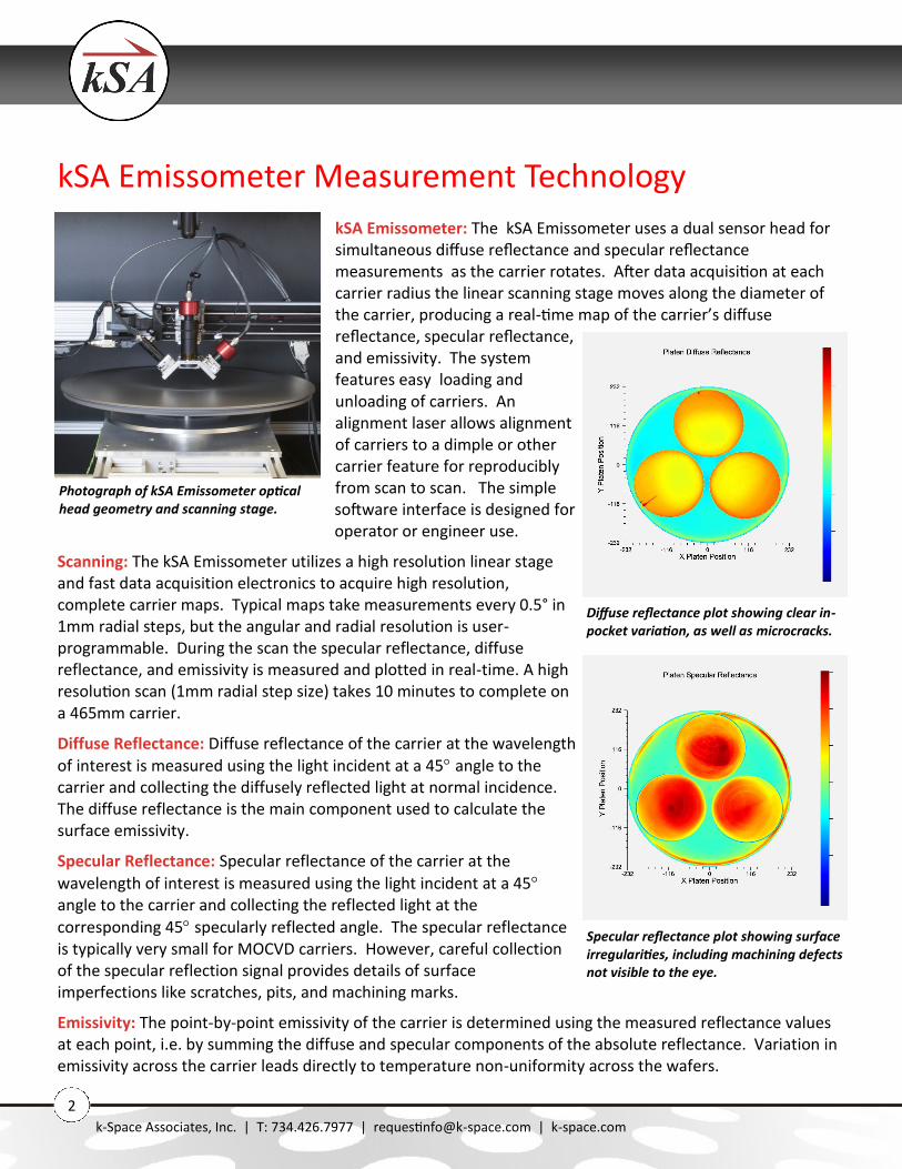
kSA Emissometer: The kSA Emissometer uses a dual sensor head for simultaneous diffuse reflectance and specular reflectance measurements as the carrier rotates. After data acquisition at each carrier radius the linear scanning stage moves along the diameter of the carrier, producing a real-time map of the carrier’s diffuse reflectance, specular reflectance, and emissivity. The system features easy loading and unloading of carriers. An alignment laser allows alignment of carriers to a dimple or other carrier feature for reproducibly from scan to scan. The simple software interface is designed for operator or engineer use.
Scanning: The kSA Emissometer utilizes a high resolution linear stage and fast data acquisition electronics to acquire high resolution, complete carrier maps. Typical maps take measurements every 0.5° in 1mm radial steps, but the angular and radial resolution is user-programmable. During the scan the specular reflectance, diffuse reflectance, and emissivity is measured and plotted in real-time. A high resolution scan (1mm radial step size) takes 10 minutes to complete on a 465mm carrier.
Diffuse Reflectance: Diffuse reflectance of the carrier at the wavelength of interest is measured using the light incident at a 45 angle to the carrier and collecting the diffusely reflected light at normal incidence. The diffuse reflectance is the main component used to calculate the surface emissivity.
Specular Reflectance: Specular reflectance of the carrier at the
wavelength of interest is measured using the light incident at a 45angle to the carrier and collecting the reflected light at the corresponding 45 specularly reflected angle. The specular reflectance is typically very small for MOCVD carriers. However, careful collection of the specular reflection signal provides details of surface imperfections like scratches, pits, and machining marks.
Emissivity: The point-by-point emissivity of the carrier is determined using the measured reflectance values at each point, i.e. by summing the diffuse and specular components of the absolute reflectance. Variation in emissivity across the carrier leads directly to temperature non-uniformity across the wafers.
Photograph of kSA Emissometer optical head geometry and scanning stage.
Diffuse reflectance plot showing clear in-pocket variation, as well as microcracks.
Specular reflectance plot showing surface irregularities, including machining defects not visible to the eye.
k-Space Associates, Inc. | T: 734.426.7977 | [email protected] | k-space.com
2

kSA Emissometer
kSA Emissometer Functional Specifications
Specifications
Carrier Diameter Up to 700mm
Carrier compatibility Spindle centering, works with most commercially-available carriers
Scanning Stage Resolution 0.05mm radial, 0.1 azimuthal, user-programmable
Scan Time 10 minutes (for a 0.1 and 1mm resolution scan of a 465mm carrier)
Detection Spot Size 2mm
Light source wavelength 940nm and 660nm (user-selectable)
Diffuse and specular reflectance resolution
± 0.005
Diffuse and specular resolution accuracy
± 0.01
Emissivity resolution ± 0.01
Emissivity accuracy ± 0.02
k-Space Associates, Inc. | T: 734.426.7977 | [email protected] | k-space.com
3
Left Plot: Full carrier scan of emissivity at 1mm radial resolution with user-defined zoom region. Right Plot: Contour plot of zoom region as defined by the circle in the left plot, showing a clear microcrack running thru the center of the carrier and extending into two wafer pockets.
kSA Emissometer
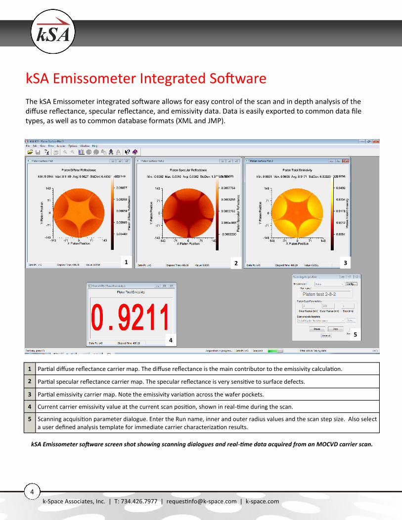
The kSA Emissometer integrated software allows for easy control of the scan and in depth analysis of the diffuse reflectance, specular reflectance, and emissivity data. Data is easily exported to common data file types, as well as to common database formats (XML and JMP).
1 Partial diffuse reflectance carrier map. The diffuse reflectance is the main contributor to the emissivity calculation.
2 Partial specular reflectance carrier map. The specular reflectance is very sensitive to surface defects.
3 Partial emissivity carrier map. Note the emissivity variation across the wafer pockets.
4 Current carrier emissivity value at the current scan position, shown in real-time during the scan.
5 Scanning acquisition parameter dialogue. Enter the Run name, inner and outer radius values and the scan step size. Also select a user defined analysis template for immediate carrier characterization results.
1 2 3
4 5
kSA Emissometer Integrated Software
k-Space Associates, Inc. | T: 734.426.7977 | [email protected] | k-space.com
4
kSA Emissometer software screen shot showing scanning dialogues and real-time data acquired from an MOCVD carrier scan.

kSA Emissometer
kSA Emissometer Analysis Features
k-Space Associates, Inc. | T: 734.426.7977 | [email protected] | k-space.com
5
Line Scan Capability: User defined lines on carrier maps generate line profiles for further analysis. The example below shows a line from the center to the edge of carrier. In this case, there is an increase in emissivity going from center to edge. This results in increased heat flux on the wafer, yielding temperature non-uniformity and ultimately poor device yield.
Web and Pocket Analysis: User may select that a Platen/carrier Report be automatically generated at the completion of the scan. This analysis tool determines pocket and web emissivity statistics over the entire web and pocket regions and as well as for the individual pocket regions. If required the user may also define exclusion regions for this analysis.
kSA Emissometer
kSA Emissometer System Specifications
k-Space Associates, Inc. | T: 734.426.7977 | [email protected] | k-space.com
6
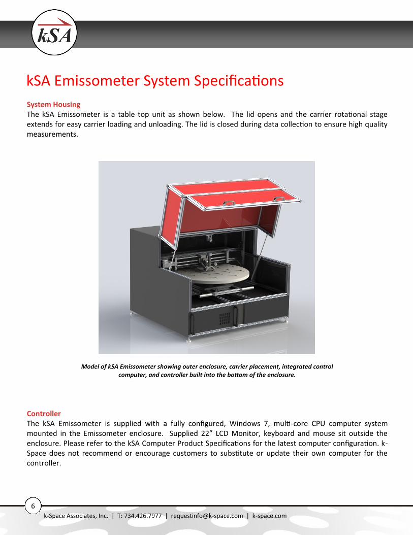
System Housing The kSA Emissometer is a table top unit as shown below. The lid opens and the carrier rotational stage extends for easy carrier loading and unloading. The lid is closed during data collection to ensure high quality measurements.
Controller The kSA Emissometer is supplied with a fully configured, Windows 7, multi-core CPU computer system mounted in the Emissometer enclosure. Supplied 22” LCD Monitor, keyboard and mouse sit outside the enclosure. Please refer to the kSA Computer Product Specifications for the latest computer configuration. k-Space does not recommend or encourage customers to substitute or update their own computer for the controller.
Model of kSA Emissometer showing outer enclosure, carrier placement, integrated control computer, and controller built into the bottom of the enclosure.

kSA Emissometer
k-Space Associates, Inc. | T: 734.426.7977 | [email protected] | k-space.com
7
kSA Emissometer System Specifications Continued
Facility Requirements Requires a flat surface (bench or table) to accommodate the specified dimensions and weight. System Power: 120 VAC with 20A max or 230 VAC with 10A max. System Dimensions: Width=104.7cm, Depth=101.6cm, and Height= 76.8cm with the lid closed. System Weight: 90.7kg (200lbs).
Installation and Training A minimum of 1-2 days of on-site customer installation and training are required with system purchase.
Warranty All kSA systems and integrated components are warranted against defective materials and workmanship for a period of ONE YEAR from the date of delivery to the original purchaser.
Left Plot: Full carrier scan of emissivity at 1mm radial resolution with user defined zoom region. Right Plot: Plot of zoom region as defined by the circle in the left plot, showing microcracks connecting the pockets, that are not visible by eye.
1
Specifications are subject to change without notice. While due caution has been exercised in the production of this document, possible errors and omissions may
occur. Emissometer Product Specs 08 FEB 16
kSA Emissometer
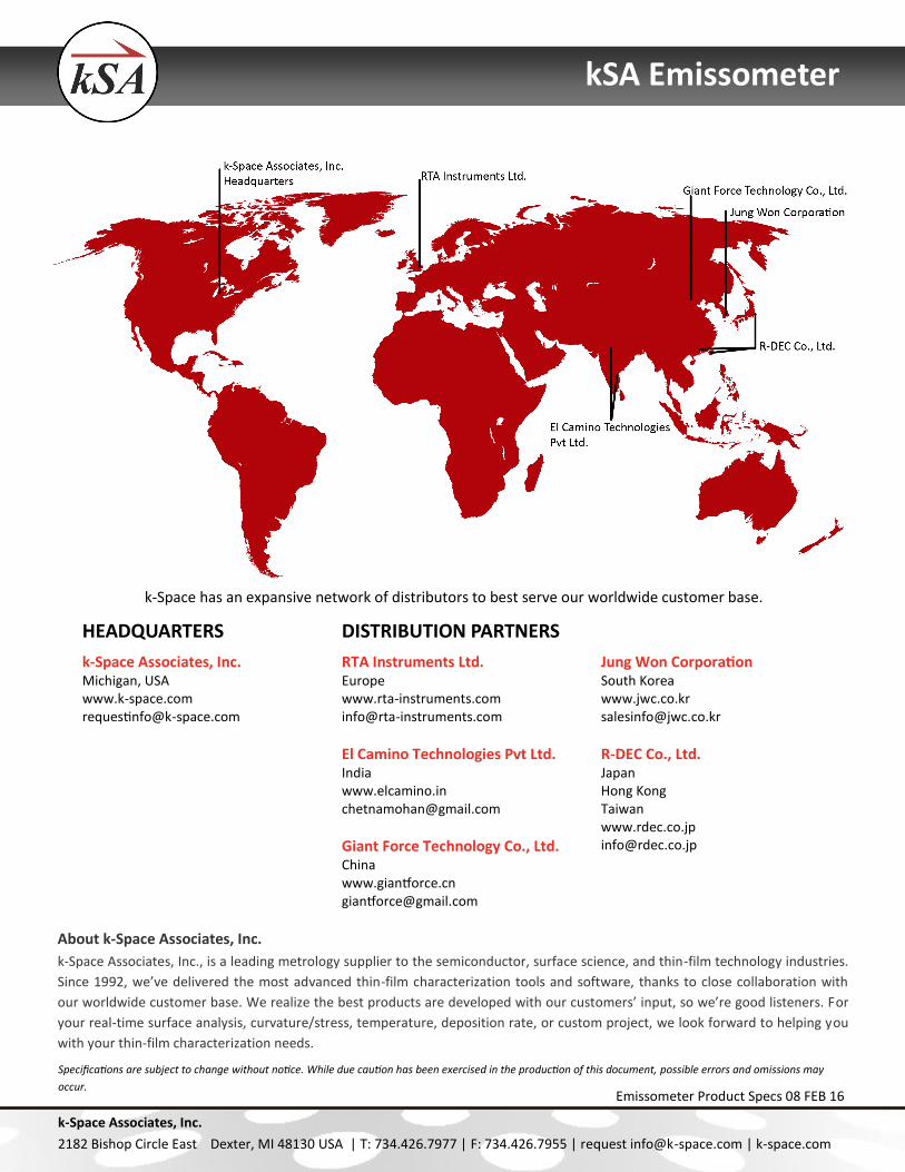
k-Space has an expansive network of distributors to best serve our worldwide customer base.
HEADQUARTERS
k-Space Associates, Inc. Michigan, USA www.k-space.com [email protected]
DISTRIBUTION PARTNERS
RTA Instruments Ltd. Europe www.rta-instruments.com [email protected]
El Camino Technologies Pvt Ltd. India www.elcamino.in [email protected]
Giant Force Technology Co., Ltd. China www.giantforce.cn [email protected]
Jung Won Corporation South Korea www.jwc.co.kr [email protected]
R-DEC Co., Ltd. Japan Hong Kong Taiwan www.rdec.co.jp [email protected]
About k-Space Associates, Inc.
k-Space Associates, Inc., is a leading metrology supplier to the semiconductor, surface science, and thin-film technology industries.
Since 1992, we’ve delivered the most advanced thin-film characterization tools and software, thanks to close collaboration with
our worldwide customer base. We realize the best products are developed with our customers’ input, so we’re good listeners. For
your real-time surface analysis, curvature/stress, temperature, deposition rate, or custom project, we look forward to helping you
with your thin-film characterization needs.
k-Space Associates, Inc.
2182 Bishop Circle East Dexter, MI 48130 USA | T: 734.426.7977 | F: 734.426.7955 | request [email protected] | k-space.com