ktt (to-263) package sheets/texas instruments pdfs... · ktt (to-263) package (top view)...
TRANSCRIPT

www.ti.com
FEATURES APPLICATIONS
1
2
3
4
5
GN
D
FEEDBACK
GND
VIN
SWITCH
COMP
KTT (TO-263) PACKAGE(TOP VIEW)
DESCRIPTION/ORDERING INFORMATION
TL3577100-kHz CURRENT-MODE SIMPLE STEP-UP/FLYBACK SWITCHING REGULATOR
SLVS633–OCTOBER 2006
• Simple Boost Converter• Few External Components Required (As FewAs Six) • Flyback Converters, Single/Multiple Outputs
• SEPIC Converter With VIN Higher or Lower• Current Limit, Undervoltage Lockout, andThan Output VoltageThermal Shutdown
• Transformer-Coupled Forward Converters• Wide Input Voltage Range: 3 V to 40 V• 100-kHz Internal Oscillator Allows for Use of
Small Magnetics• Current-Mode Operation for Faster Transient
Response, Line Regulation, andCycle-by-Cycle Current Limiting
• Soft-Start Capability Provides ControlledStartup Current
• Improved Replacement for LM2577 Series
The TL3577 series are easy-to-use devices that incorporate all the active circuitry required to implement eitherstep-up (boost), flyback, forward converter, or SEPIC converter switching regulators. The internal 3-A 65-Vswitch allows the TL3577 to provide an output voltage of up to 60 V as a simple boost regulator; higher outputvoltages can be achieved with the TL3577 configured as a flyback or forward converter.
Requiring few external components, The TL3577 features a wide input voltage range of 3 V to 40 V and offersan adjustable output voltage. Basic protection features include undervoltage lockout, thermal protection, and softstart, which is provided to reduce input current during startup. Current-mode control provides cycle-by-cyclecurrent limiting, as well as faster line and load regulation. The internal 100-kHz oscillator allows for use ofsmaller magnetics and filter components, when compared with similar regulators running at 52 kHz. A standardseries of inductors and capacitors optimized for use with these regulators is available from severalmanufacturers and are listed in this data sheet.
The TL3577 is characterized for operation over the virtual junction temperature range of –40°C to 125°C.
ORDERING INFORMATION
VOTJ PACKAGE (1) ORDERABLE PART NUMBER TOP-SIDE MARKING(NOM)
–40°C to 125°C ADJ TO-263 – KTT Reel of 500 TL3577-ADJIKTTR TL3577ADJI
(1) Package drawings, standard packing quantities, thermal data, symbolization, and PCB design guidelines are available atwww.ti.com/sc/package.
Please be aware that an important notice concerning availability, standard warranty, and use in critical applications of TexasInstruments semiconductor products and disclaimers thereto appears at the end of this data sheet.
PRODUCTION DATA information is current as of publication date. Copyright © 2006, Texas Instruments IncorporatedProducts conform to specifications per the terms of the TexasInstruments standard warranty. Production processing does notnecessarily include testing of all parameters.
www.ti.com
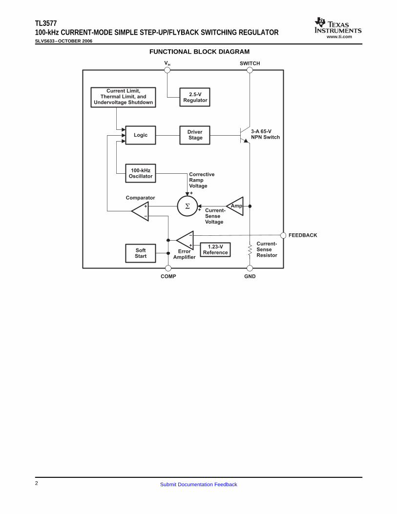
2.5-VRegulator
DriverStage
1.23-VReference
100-kHzOscillator
SoftStart
Logic
Current Limit,Thermal Limit, and
Undervoltage Shutdown
AmpS
Comparator
ErrorAmplifier
VIN SWITCH
FEEDBACK
GNDCOMP
CorrectiveRampVoltage
+
+
Current-SenseVoltage
Current-SenseResistor
3-A 65-VNPN Switch
TL3577100-kHz CURRENT-MODE SIMPLE STEP-UP/FLYBACK SWITCHING REGULATORSLVS633–OCTOBER 2006
FUNCTIONAL BLOCK DIAGRAM
2 Submit Documentation Feedback

www.ti.com
Absolute Maximum Ratings (1)
Package Thermal Data (1)
Recommended Operating Conditions
TL3577100-kHz CURRENT-MODE SIMPLE STEP-UP/FLYBACK SWITCHING REGULATOR
SLVS633–OCTOBER 2006
over operating free-air temperature range (unless otherwise noted)
MIN MAX UNIT
VIN Supply voltage 45 V
VSW Output SWITCH voltage 65 V
ISW Output SWITCH current 6 A
TJ Maximum junction temperature 150 °C
Tstg Storage temperature range –65 150 °C
TJ Junction temperature 150 °C
(1) Stresses beyond those listed under "absolute maximum ratings" may cause permanent damage to the device. These are stress ratingsonly, and functional operation of the device at these or any other conditions beyond those indicated under "recommended operatingconditions" is not implied. Exposure to absolute-maximum-rated conditions for extended periods may affect device reliability.
PACKAGE BOARD θJA θJC θJCB
TO-263 (KTT) High K, JESD 51-5 31.8 35.0 1.13
(1) Maximum power dissipation is a function of TJ(max), θJA, and TA. The maximum allowable power dissipation at any allowable ambienttemperature is PD = (TJ(max) – TA)/θJA. Operating at the absolute maximum TJ of 150°C can affect reliability.
over operating free-air temperature range (unless otherwise noted)
MIN MAX UNIT
VIN Supply voltage 3 40 V
VSW Output SWITCH voltage 0 60 V
ISW Output SWITCH current 3 A
TJ Operating virtual junction temperature –40 125 °C
3Submit Documentation Feedback

www.ti.com
Electrical Characteristics
DVOUT
DVIN
DVOUT
DILOAD
DVREF
DVIN
DISWITCH
DVCOMP
TL3577100-kHz CURRENT-MODE SIMPLE STEP-UP/FLYBACK SWITCHING REGULATORSLVS633–OCTOBER 2006
VIN = 5 V, VFEEDBACK = VREF, ISWITCH = 0 (unless otherwise noted)
TL3577-ADJPARAMETER TEST CONDITIONS TJ UNIT
MIN TYP MAX
25°C 11.6 12 12.4VIN = 5 V to 10 V,VOUT Output voltage VILOAD = 100 mA to 800 mA, See Figure 1 Full range 11.4 12.6
25°C 20 50VIN = 3.5 V to 10 V, ILOAD = 200 mA,Line regulation mVSee Figure 1 Full range 100
25°C 20 50Load regulation ILOAD = 100 mA to 800 mA, See Figure 1 mV
Full range 100
η Efficiency ILOAD = 800 mA, See Figure 1 25°C 80 %
25°C 7.5 10VFEEDBACK = 1.5 V (SWITCH Off)
Full range 14ICC Input supply current mA
25°C 45 70ISWITCH = 2 A,VCOMP = 2 V (maximum duty cycle) Full range 85
25°C 2.7 2.85VUV Input supply undervoltage lockout ISWITCH = 100 mA V
Full range 2.95
25°C 85 100 115fO Oscillator frequency Measured at SWITCH, ISWITCH = 100 mA kHz
Full range 80 120
25°C 1.214 1.23 1.246Measured at FEEDBACK,VREF Reference voltage VVIN = 3 V to 40 V, VCOMP = 1 V Full range 1.206 1.254
Reference voltage line regulation VIN = 3 V to 40 V 25°C 0.5 mV
25°C 100 300IB Error amplifier input bias current VCOMP = 1 V nA
Full range 800
25°C 2400 3700 4800GM Error amplifier transconductance ICOMP = –30 µA to 30 µA, VCOMP = 1 V µmho
Full range 1600 5800
25°C 500 800AVOL Error amplifier voltage gain VCOMP = 1.1 V to 1.9 V, RCOMP = 1 MΩ (1) V/V
Full range 250
25°C 2.2 2.4Upper limit, VFEEDBACK = 1 V
Full range 2Error amplifier output swing V
25°C 0.3 0.4Lower limit, VFEEDBACK = 1.5 V
Full range 0.55
25°C ±130 ±200 ±300Error amplifier output current VFEEDBACK = 1 V to 1.5 V, VCOMP = 1 V µA
Full range ±90 ±400
25°C 2.5 5 7.5ISS Soft-start current VFEEDBACK = 1 V, VCOMP = 0 µA
Full range 1.5 9.5
25°C 88 90D Maximum duty cyle VCOMP = 1.5 V, ISWITCH = 100 mA %
Full range 84
Switch transconductance 25°C 12.5 A/V
25°C 10 300VSWITCH = 65 V,IL Switch leakage current µAVFEEDBACK = 1.5 V (SWITCH off) Full range 600
25°C 0.5 0.7ISWITCH = 2 A,VSAT Switch saturation voltage VVCOMP = 2 V (maximum duty cycle) Full range 0.9
25°C 3.7 4.3 5.3NPN switch current limit VCOMP = 2 V A
Full range 3 6
(1) A 1-MΩ resistor is connected to the compensation pin (which is the error amplifier output) to ensure accuracy in measuring AVOL. Inactual applications, this load resistance should be ≥10 MΩ, resulting in AVOL that is typically twice the specified minimum limit.
4 Submit Documentation Feedback

www.ti.com
TL3577100-kHz CURRENT-MODE SIMPLE STEP-UP/FLYBACK SWITCHING REGULATOR
SLVS633–OCTOBER 2006
Electrical Characteristics (continued)VIN = 5 V, VFEEDBACK = VREF, ISWITCH = 0 (unless otherwise noted)
TL3577-ADJPARAMETER TEST CONDITIONS TJ UNIT
MIN TYP MAX
25°C 25 40COMP current VCOMP = 0 V µA
Full range 50
5Submit Documentation Feedback

www.ti.com
TYPICAL CHARACTERISTICS
-0.2
-0.1
0
0.1
0.2
0.3
0.4
0.5
0 5 10 15 20 25 30 35 40
VIN – Supply Voltage – V
Ref
eren
ceV
olta
ge–
mV
∆1.23
1.232
1.234
1.236
1.238
1.24
1.242
1.244
1.246
1.248
1.25
-40 -25 -10 5 20 35 50 65 80 95 110 125
TA – Temperature – °C
VR
EF
–R
efer
ence
Vol
tage
–V
600
700
800
900
1000
1100
1200
1300
1400
1500
1600
-40 -25 -10 5 20 35 50 65 80 95 110 125
TA – Temperature – °C
AV
–E
rror
Am
plifi
erV
olta
geG
ain
–V
/V
2500
2750
3000
3250
3500
3750
4000
4250
4500
4750
5000
-40 -25 -10 5 20 35 50 65 80 95 110 125
TA – Temperature – °C
GM
–E
rror
Am
plifi
erT
rans
cond
ucta
nce
–µ
mho
TL3577100-kHz CURRENT-MODE SIMPLE STEP-UP/FLYBACK SWITCHING REGULATORSLVS633–OCTOBER 2006
REFERENCE VOLTAGE ∆ REFERENCE VOLTAGEvs vs
TEMPERATURE SUPPLY VOLTAGE
ERROR AMPLIFIER TRANSCONDUCTANCE ERROR AMPLIFIER VOLTAGE GAINvs vs
TEMPERATURE TEMPERATURE
6 Submit Documentation Feedback

www.ti.com
4
4.2
4.4
4.6
4.8
5
5.2
5.4
5.6
5.8
6
-40 -25 -10 5 20 35 50 65 80 95 110 125
TA – Temperature – °C
Sw
itch
Cur
rent
Lim
it–
A6
6.5
7
7.5
8
8.5
9
9.5
10
10.5
11
-40 -25 -10 5 20 35 50 65 80 95 110 125
TA – Temperature – °C
I Q–
Qui
esce
ntC
urre
nt–
mA
90
92
94
96
98
100
102
104
106
108
110
-40 -25 -10 5 20 35 50 65 80 95 110 125
TA – Temperature – °C
f O–
Osc
illat
orF
requ
ency
–kH
z
30
40
50
60
70
80
90
100
110
120
130
-40 -25 -10 5 20 35 50 65 80 95 110 125
TA – Temperature – °C
I B–
FE
ED
BA
CK
Bia
sC
urre
nt–
nA
TL3577100-kHz CURRENT-MODE SIMPLE STEP-UP/FLYBACK SWITCHING REGULATOR
SLVS633–OCTOBER 2006
TYPICAL CHARACTERISTICS (continued)
QUIESCENT CURRENT SWITCH CURRENT LIMITvs vs
TEMPERATURE TEMPERATURE
FEEDBACK BIAS CURRENT OSCILLATOR FREQUENCYvs vs
TEMPERATURE TEMPERATURE
7Submit Documentation Feedback

www.ti.com
0.3
0.35
0.4
0.45
0.5
0.55
0.6
0.65
0.7
0.75
0.8
0.85
0.9
-40 -25 -10 5 20 35 50 65 80 95 110 125
TA – Temperature – °C
VS
AT
–S
witc
hS
atur
atio
nV
olta
ge–
V
ISW = 2 A
VCOMP = 2 V
TL3577100-kHz CURRENT-MODE SIMPLE STEP-UP/FLYBACK SWITCHING REGULATORSLVS633–OCTOBER 2006
TYPICAL CHARACTERISTICS (continued)
SWITCH SATURATION VOLTAGEvs
TEMPERATURE
8 Submit Documentation Feedback

www.ti.com
PARAMETER MEASUREMENT INFORMATION
TL3577-ADJ
VIN
COMP
GND
FEEDBACK
SWITCH
LOAD
VIN
C
680 µFOUT
0.1 µF24 W60 W120 W
100 µH
220 µF
2 kW
0.1 µF
0.33 µF
SW1 SW2
R1
R2
10 kW
TL3577100-kHz CURRENT-MODE SIMPLE STEP-UP/FLYBACK SWITCHING REGULATOR
SLVS633–OCTOBER 2006
A. R1 = 48.7 kΩ in series with 511 ΩB. R2 = 5.62 kΩ (1%)
Figure 1. Test Circuit
9Submit Documentation Feedback

www.ti.com
APPLICATION INFORMATION
TL3577-ADJ
VIN
COMP
GND
FEEDBACK
SWITCH
12 V at 800 mA
Regulated Output
£100 µH
2.2 kW
0.1 µF
0.33 µF
17.4 kW
2 kW
5-VInput
680 µF
TL3577-ADJ
VIN
COMP
GND
FEEDBACK
SWITCH
47 µH
100 µF
2.4 kΩ
0.47 µF
1:2.5
1 µF
5 V(4 V to 6 V)
12 V at 150 mA
12 V at 150 mA
330 µF
330 µF
2 kΩ
17.4 kΩ
TL3577100-kHz CURRENT-MODE SIMPLE STEP-UP/FLYBACK SWITCHING REGULATORSLVS633–OCTOBER 2006
Figure 2 shows a typical application of the TL3577 in a boost regulator.
Figure 2. Typical Application – Boost Regulator
Figure 3 shows a typical application of the TL3577 in a flyback regulator.
Figure 3. Typical Application – Flyback Regulator
10 Submit Documentation Feedback

www.ti.com
TL3577-ADJ
VIN
COMP
GND
FEEDBACK
SWITCH
100 µH
10 kΩ
22 µF
680 pF
Input3 V to 12 V 1 µF
(See Note A)
100 µH
10 µF12.1 kΩ
20 kΩOutput3.3 V
TL3577100-kHz CURRENT-MODE SIMPLE STEP-UP/FLYBACK SWITCHING REGULATOR
SLVS633–OCTOBER 2006
APPLICATION INFORMATION (continued)
Figure 4 shows a typical application of the TL3577 in a SEPIC regulator.
A. Low ESR. Voltage rating must be at least VIN + VOUT.
Figure 4. Typical Application – SEPIC Regulator
11Submit Documentation Feedback
www.ti.com
Step-Up (Boost) Regulator
Step-Up Regulator Design Procedure
VSW(OFF)
VSAT
0 V
0 V
0
0
0
VF
VR
IIND(AVG)
ISW(PK)
ID(PK)
ID(AVG)
∆IIND
SwitchVoltage
DiodeVoltage
InductorCurrent
SwitchCurrent
DiodeCurrent
TL3577100-kHz CURRENT-MODE SIMPLE STEP-UP/FLYBACK SWITCHING REGULATORSLVS633–OCTOBER 2006
APPLICATION INFORMATION (continued)
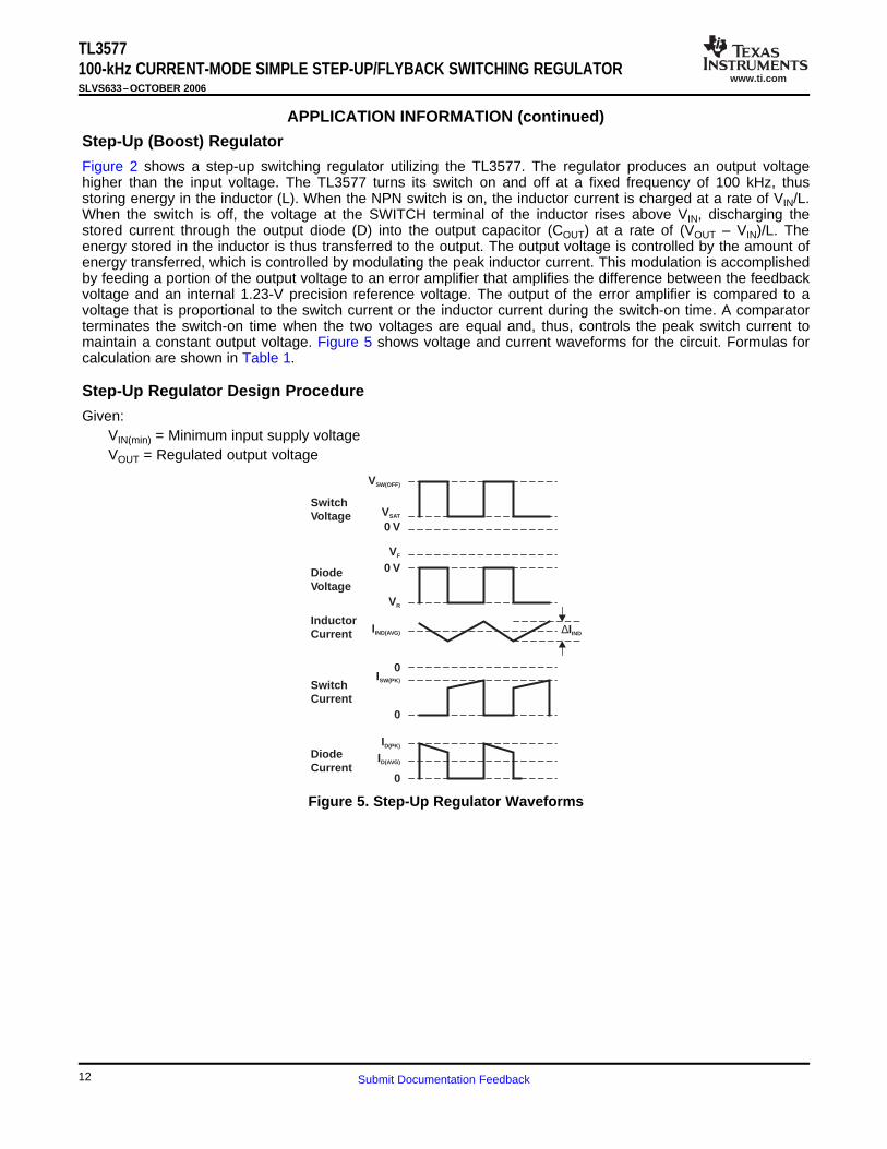
Figure 2 shows a step-up switching regulator utilizing the TL3577. The regulator produces an output voltagehigher than the input voltage. The TL3577 turns its switch on and off at a fixed frequency of 100 kHz, thusstoring energy in the inductor (L). When the NPN switch is on, the inductor current is charged at a rate of VIN/L.When the switch is off, the voltage at the SWITCH terminal of the inductor rises above VIN, discharging thestored current through the output diode (D) into the output capacitor (COUT) at a rate of (VOUT – VIN)/L. Theenergy stored in the inductor is thus transferred to the output. The output voltage is controlled by the amount ofenergy transferred, which is controlled by modulating the peak inductor current. This modulation is accomplishedby feeding a portion of the output voltage to an error amplifier that amplifies the difference between the feedbackvoltage and an internal 1.23-V precision reference voltage. The output of the error amplifier is compared to avoltage that is proportional to the switch current or the inductor current during the switch-on time. A comparatorterminates the switch-on time when the two voltages are equal and, thus, controls the peak switch current tomaintain a constant output voltage. Figure 5 shows voltage and current waveforms for the circuit. Formulas forcalculation are shown in Table 1.
Given:VIN(min) = Minimum input supply voltageVOUT = Regulated output voltage
Figure 5. Step-Up Regulator Waveforms
12 Submit Documentation Feedback

www.ti.com
V + V – VOUT F IN V – VOUT IN
V + V – VOUT F SAT VOUT
≈
ILOAD
1 – D
V – VIN SAT D
L 100,000•
ILOAD ∆IIND
1 – D 2+
ILOAD ∆IIND
1 – D 2+
V + VOUT F
V – VOUT SAT
ILOAD
ILOAD ∆IIND
1 – D 2+
ILOAD I D VLOAD IN• •
1 – D 50 (1 – D)+0.25 Ω ( (
2
D
1. Output Voltage Section
2. Inductor Selection (L)
TL3577100-kHz CURRENT-MODE SIMPLE STEP-UP/FLYBACK SWITCHING REGULATOR
SLVS633–OCTOBER 2006
Table 1. Step-up Regulator Formulas (1)
Duty cycle D
Average inductor current IIND(AVG)
Inductor current ripple ∆IIND
Peak inductor current IIND(PK)
Peak switch current ISW(PK)
Switch voltage when off VSW(OFF)
Diode reverse voltage VR
Average diode current ID(AVG)
Peak diode current ID(PK)
Power dissipation PD
(1) VF = forward-biased diode voltage, ILOAD = output load
First, determine if the TL3577 can provide these values of VOUT and ILOAD(max) when operating with the minimumvalue of VIN. The upper limits for VOUT and ILOAD(max) are given by the following equations.
VOUT ≤ 60 V andVOUT ≤ 10 × VIN
ILOAD(max) ≤ (2.1 A × VIN(min))/VOUT
These limits must be greater than or equal to the values specified in this application.
Resistors R1 and R2 are used to select the desired output voltage. These resistors form a voltage divider andpresent a portion of the output voltage to the error amplifier, which compares it to an internal 1.23-V reference.Select R1 and R2 such that:
R1/R2 = (VOUT/1.23 V) – 1
A. Preliminary Calculations
To select the inductor, the calculation of the following three parameters is necessary:Dmax, the maximum switch duty cycle (0 ≤ D ≤ 0.9):
Dmax = VOUT + VF – VIN(min)/VOUT + VF – 0.6 Vwhere, typically, VF = 0.5 V for Schottky diodes and VF = 0.8 V for fast-recovery diodes.
E • T, the product of volts • time that charges the inductor:E • T = Dmax × (VIN(min) – 0.6V)106/100,000 Hz (Vµs)
IIND,DC, the average inductor current under full load:IIND,DC = (1.05 × ILOAD(max))/(1 – Dmax)
13Submit Documentation Feedback

www.ti.com
0.3 0.4 0.450.35 0.5 0.6 0.7 0.8 0.9 1.0 1.5 2.0 2.5 3.020
30
35
25
40
45
50
60
70
80
90100
200
150
L47
L68L100L150L220L330
H2200
L680
H1500 H1000 H680 H470 H330 H220
H150
L470
E •
T (
V •
µs)
I (A)IND,DC
TL3577100-kHz CURRENT-MODE SIMPLE STEP-UP/FLYBACK SWITCHING REGULATORSLVS633–OCTOBER 2006
B. Identify Inductor Value1. From Figure 6, identify the inductor code for the region indicated by the intersection of E • T and IIND,DC. This
code gives the inductor value in microhenries. The L or H prefix signifies whether the inductor is rated for amaximum E • T of 90 Vµs (L) or 250 Vµs (H).
2. If D < 0.85, go to step C. If D ≥ 0.85, calculate the minimum inductance needed to ensure the switchingregulator’s stability:
If Lmin is smaller than the inductor values found in step B1, go on to step C. Otherwise, the inductor valuefound in step 1, above, is too low; an appropriate inductor code should be obtained from Figure 6 as follows:a. Find the lowest-value inductor that is greater than Lmin.b. Find where E • T intersects this inductor value to determine if it has an L or H prefix. If E • T intersects
both the L and H regions, select the inductor with an H prefix.
C. Inductor Selection
Select an inductor from Table 2 which cross references the inductor codes to the part numbers of the threedifferent manufacturers. The inductors listed in Table 2 have the following characteristics:
AIE (ferrite, pot-core inductors): Benefits of this type are low electromagnetic interference (EMI), smallphysical size, and very low power dissipation (core loss).Pulse (powdered iron, toroid core inductors): Benefits are low EMI and ability to withstand E • T and peakcurrent above rated value better than ferrite cores.Renco (ferrite, bobbin-core inductors): Benefits are low cost and best ability to withstand E • T and peakcurrent above rated value. Be aware that these inductors generate more EMI than the other types, and thismay interfere with signals sensitive to noise.
A. This chart assumes that the inductor ripple current inductor is approximately 20% to 30% of the average inductorcurrent (when the regulator is under full load). Greater ripple current causes higher peak switch currents and greateroutput ripple voltage. Lower ripple current is achieved with larger value inductors. The factor of 20% to 30% ischosen as a convenient balance between the two extremes.
Figure 6. Inductor Selection Graph
14 Submit Documentation Feedback

www.ti.com
3. Compensation Network (RC, CC) and Output Capacitor (COUT) Selection
TL3577100-kHz CURRENT-MODE SIMPLE STEP-UP/FLYBACK SWITCHING REGULATOR
SLVS633–OCTOBER 2006
Table 2. Standardized Inductors and Manufacturer’s Part Numbers
Manufacturer’s Part NumberInductor Code
AIE (1) Pulse (2) Renco (3)
L47 415 - 0932 PE - 53112 RL2442
L68 415 - 0931 PE - 92114 RL2443
L100 415 - 0930 PE - 92108 RL2444
L150 415 - 0953 PE - 53113 RL1954
L220 415 - 0922 PE - 52626 RL1953
L330 415 - 0926 PE - 52627 RL1952
L470 415 - 0927 PE - 53114 RL1951
L680 415 - 0928 PE - 52629 RL1950
H150 415 - 0936 PE - 53115 RL2445
H220 430 - 0636 PE - 53116 RL2446
H330 430 - 0635 PE - 53117 RL2447
H470 430 - 0634 PE - 53118 RL1961
H680 415 - 0935 PE - 53119 RL1960
H1000 415 - 0934 PE - 53120 RL1959
H1500 415 - 0933 PE - 53121 RL1958
H2200 415 - 0945 PE - 53122 RL2448
(1) AIE Magnetics, Div. Vernitron Corp., (813) 347-2181 2801 72nd Street North, St. Petersburg, FL 33710(2) Pulse Engineering, (619) 674-8100 12220 World Trade Drive, San Diego, CA 92128(3) Renco Electronics, Inc., (516) 586-5566 60 Jeffryn Blvd. East, Deer Park, NY 11729
The compensation network consists of resistor RC and capacitor CC, which form a simple pole-zero network andstabilize the regulator. The values of RC and CC depend upon the voltage gain of the regulator, ILOAD(max), theinductor L, and output capacitance COUT. A procedure to calculate and select the values for RC, CC, and COUTthat ensures stability is described below. It should be noted, however, that this may not result in optimumcompensation. To guarantee optimum compensation, a standard procedure for testing loop stability isrecommended, such as measuring VOUT transient responses to pulsing ILOAD.
A. Calculate the maximum value for RC.
RC ≤ (750 × ILOAD(max) × VOUT2)/VIN(min)
2
Select a resistor less than or equal to this value, not to exceed 3 kΩ.
B. Calculate the minimum value for COUT using the following two equations.
COUT ≥ (0.19 × L × RC × ILOAD(max))/(VIN(min) × VOUT) and
COUT ≥ (VIN(min) × RC × (VIN(min) + (3.74 × 10⁵ × L))/(487,800 × VOUT3)
The larger of these two values is the minimum value that ensures stability.
15Submit Documentation Feedback

www.ti.com
4. Input Capacitor Selection (CIN)
TL3577100-kHz CURRENT-MODE SIMPLE STEP-UP/FLYBACK SWITCHING REGULATORSLVS633–OCTOBER 2006
C. Calculate the minimum value of CC.
CC ≥ 58.5 × VOUT2 × COUT × RC
2 × VIN(min)
The compensation capacitor also is used in the soft-start function of the regulator. When the input voltage isapplied to the part, the switch duty cycle is increased slowly at a rate defined by the compensation capacitor andthe soft-start current, thus eliminating high input currents. Without the soft-start circuitry, the switch duty cyclewould instantly rise to about 90% and draw large currents from the input supply. For proper soft starting, thevalue for CC should be equal to or greater than 0.22 µF.
Table 3 lists several types of aluminum electrolytic capacitors that could be used for the output filter. Use thefollowing parameters to select the capacitor:
Working Voltage (WVDC): Choose a capacitor with a working voltage at least 20% higher than the regulatoroutput voltage.
Ripple Current: This is the maximum RMS value of current that charges the capacitor during each switchingcycle. For step-up and flyback regulators, the formula for ripple current is:
IRIPPLE(rms) = (ILOAD(max) × Dmax)/(1 – Dmax)
Choose a capacitor that is rated at least 50% higher than this value at 100 kHz.
Equivalent Series Resistance (ESR): This is the primary cause of output ripple voltage, and it also affects thevalues of RC and CC needed to stabilize the regulator. As a result, the preceding calculations for CC and RC areonly valid if the ESR does not exceed the maximum value specified by the following equations.
ESR ≤ (0.01 × 15 V)/IRIPPLE(P-P) and ≤ (8.7 × 10⁻³ × VIN)/ILOAD(max) whereIRIPPLE(P-P) = (1.15 × ILOAD(max))/(1 – Dmax)
Select a capacitor with an ESR, at 100 kHz, that is less than or equal to the lower value calculated. Mostelectrolytic capacitors specify ESR at 120 kHz, which is 15% to 30% higher than at 100 kHz. Also, note thatESR increases by a factor of 2 when operating at –20°C.
In general, low values of ESR are achieved by using large-value capacitors (C ≥ 470 µF) and capacitors withhigh WVDC, or by paralleling smaller-value capacitors.
To reduce noise on the supply voltage caused by the switching action of a step-up regulator (ripple currentnoise), VIN should be bypassed to ground. A good quality 0.1-µF capacitor with low ESR should providesufficient decoupling. If the TL3577 is located far from the supply-source filter capacitors, an additionalelectrolytic (47 µF, for example) is required.
Table 3. Aluminum Electrolytic Capacitors Recommended for Switching Regulators
Nichicon – Types PF, PX, or PZ United Chemi-CON – Types LX, SXF, or SXJ927 East State Parkway, Schaumburg, IL 60173 9801West Higgens, Rosemont, IL 60018
(708) 843-7500 (708) 696-2000
16 Submit Documentation Feedback
www.ti.com
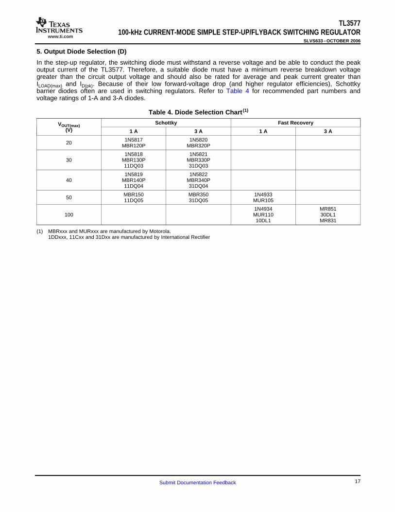
5. Output Diode Selection (D)
TL3577100-kHz CURRENT-MODE SIMPLE STEP-UP/FLYBACK SWITCHING REGULATOR
SLVS633–OCTOBER 2006
In the step-up regulator, the switching diode must withstand a reverse voltage and be able to conduct the peakoutput current of the TL3577. Therefore, a suitable diode must have a minimum reverse breakdown voltagegreater than the circuit output voltage and should also be rated for average and peak current greater thanILOAD(max) and ID(pk). Because of their low forward-voltage drop (and higher regulator efficiencies), Schottkybarrier diodes often are used in switching regulators. Refer to Table 4 for recommended part numbers andvoltage ratings of 1-A and 3-A diodes.
Table 4. Diode Selection Chart (1)
Schottky Fast RecoveryVOUT(max)(V) 1 A 3 A 1 A 3 A
1N5817 1N582020 MBR120P MBR320P
1N5818 1N582130 MBR130P MBR330P
11DQ03 31DQ03
1N5819 1N582240 MBR140P MBR340P
11DQ04 31DQ04
MBR150 MBR350 1N493350 11DQ05 31DQ05 MUR105
1N4934 MR851100 MUR110 30DL1
10DL1 MR831
(1) MBRxxx and MURxxx are manufactured by Motorola.1DDxxx, 11Cxx and 31Dxx are manufactured by International Rectifier
17Submit Documentation Feedback
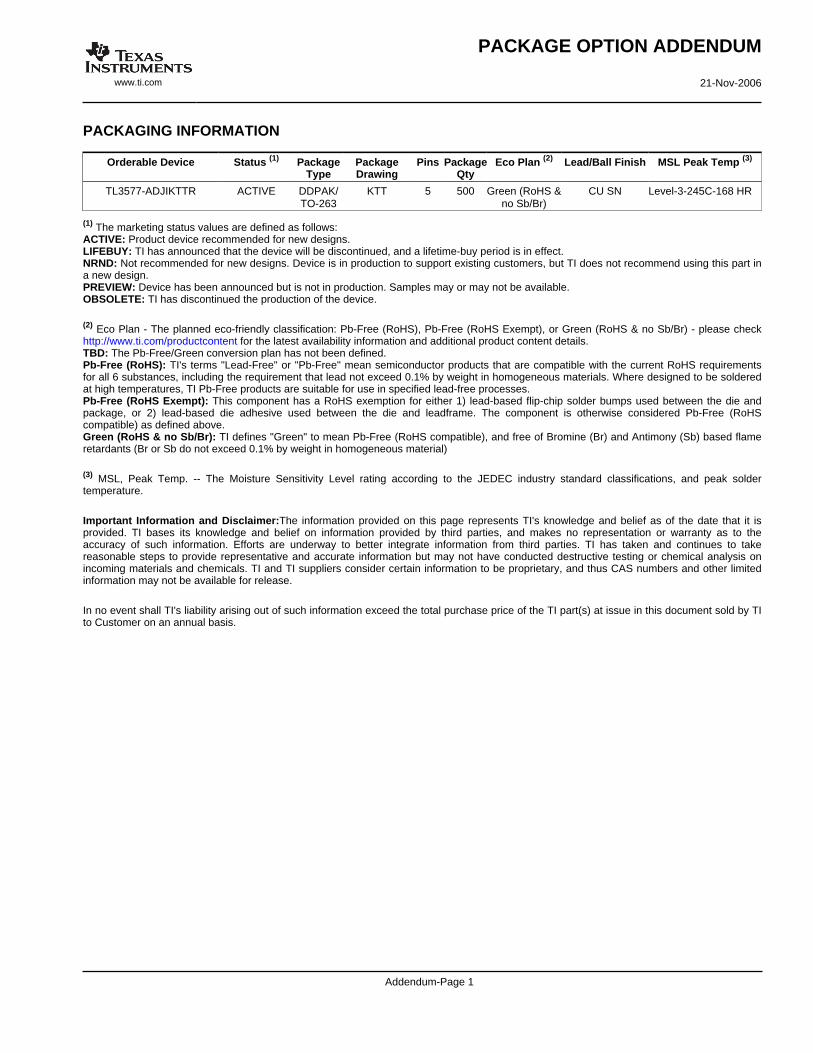
PACKAGING INFORMATION
Orderable Device Status (1) PackageType
PackageDrawing
Pins PackageQty
Eco Plan (2) Lead/Ball Finish MSL Peak Temp (3)
TL3577-ADJIKTTR ACTIVE DDPAK/TO-263
KTT 5 500 Green (RoHS &no Sb/Br)
CU SN Level-3-245C-168 HR
(1) The marketing status values are defined as follows:ACTIVE: Product device recommended for new designs.LIFEBUY: TI has announced that the device will be discontinued, and a lifetime-buy period is in effect.NRND: Not recommended for new designs. Device is in production to support existing customers, but TI does not recommend using this part ina new design.PREVIEW: Device has been announced but is not in production. Samples may or may not be available.OBSOLETE: TI has discontinued the production of the device.
(2) Eco Plan - The planned eco-friendly classification: Pb-Free (RoHS), Pb-Free (RoHS Exempt), or Green (RoHS & no Sb/Br) - please checkhttp://www.ti.com/productcontent for the latest availability information and additional product content details.TBD: The Pb-Free/Green conversion plan has not been defined.Pb-Free (RoHS): TI's terms "Lead-Free" or "Pb-Free" mean semiconductor products that are compatible with the current RoHS requirementsfor all 6 substances, including the requirement that lead not exceed 0.1% by weight in homogeneous materials. Where designed to be solderedat high temperatures, TI Pb-Free products are suitable for use in specified lead-free processes.Pb-Free (RoHS Exempt): This component has a RoHS exemption for either 1) lead-based flip-chip solder bumps used between the die andpackage, or 2) lead-based die adhesive used between the die and leadframe. The component is otherwise considered Pb-Free (RoHScompatible) as defined above.Green (RoHS & no Sb/Br): TI defines "Green" to mean Pb-Free (RoHS compatible), and free of Bromine (Br) and Antimony (Sb) based flameretardants (Br or Sb do not exceed 0.1% by weight in homogeneous material)
(3) MSL, Peak Temp. -- The Moisture Sensitivity Level rating according to the JEDEC industry standard classifications, and peak soldertemperature.
Important Information and Disclaimer:The information provided on this page represents TI's knowledge and belief as of the date that it isprovided. TI bases its knowledge and belief on information provided by third parties, and makes no representation or warranty as to theaccuracy of such information. Efforts are underway to better integrate information from third parties. TI has taken and continues to takereasonable steps to provide representative and accurate information but may not have conducted destructive testing or chemical analysis onincoming materials and chemicals. TI and TI suppliers consider certain information to be proprietary, and thus CAS numbers and other limitedinformation may not be available for release.
In no event shall TI's liability arising out of such information exceed the total purchase price of the TI part(s) at issue in this document sold by TIto Customer on an annual basis.
PACKAGE OPTION ADDENDUM
www.ti.com 21-Nov-2006
Addendum-Page 1


IMPORTANT NOTICE
Texas Instruments Incorporated and its subsidiaries (TI) reserve the right to make corrections, modifications, enhancements, improvements, and other changes to its products and services at any time and to discontinue any product or service without notice. Customers should obtain the latest relevant information before placing orders and should verify that such information is current and complete. All products are sold subject to TI’s terms and conditions of sale supplied at the time of order acknowledgment. TI warrants performance of its hardware products to the specifications applicable at the time of sale in accordance with TI’s standard warranty. Testing and other quality control techniques are used to the extent TI deems necessary to support this warranty. Except where mandated by government requirements, testing of all parameters of each product is not necessarily performed. TI assumes no liability for applications assistance or customer product design. Customers are responsible for their products and applications using TI components. To minimize the risks associated with customer products and applications, customers should provide adequate design and operating safeguards. TI does not warrant or represent that any license, either express or implied, is granted under any TI patent right, copyright, mask work right, or other TI intellectual property right relating to any combination, machine, or process in which TI products or services are used. Information published by TI regarding third-party products or services does not constitute a license from TI to use such products or services or a warranty or endorsement thereof. Use of such information may require a license from a third party under the patents or other intellectual property of the third party, or a license from TI under the patents or other intellectual property of TI. Reproduction of information in TI data books or data sheets is permissible only if reproduction is without alteration and is accompanied by all associated warranties, conditions, limitations, and notices. Reproduction of this information with alteration is an unfair and deceptive business practice. TI is not responsible or liable for such altered documentation. Resale of TI products or services with statements different from or beyond the parameters stated by TI for that product or service voids all express and any implied warranties for the associated TI product or service and is an unfair and deceptive business practice. TI is not responsible or liable for any such statements. Following are URLs where you can obtain information on other Texas Instruments products and application solutions: Products Applications Amplifiers amplifier.ti.com Audio www.ti.com/audio Data Converters dataconverter.ti.com Automotive www.ti.com/automotive DSP dsp.ti.com Broadband www.ti.com/broadband Interface interface.ti.com Digital Control www.ti.com/digitalcontrol Logic logic.ti.com Military www.ti.com/military Power Mgmt power.ti.com Optical Networking www.ti.com/opticalnetwork Microcontrollers microcontroller.ti.com Security www.ti.com/security Low Power Wireless www.ti.com/lpw Telephony www.ti.com/telephony Video & Imaging www.ti.com/video Wireless www.ti.com/wireless Mailing Address: Texas Instruments Post Office Box 655303 Dallas, Texas 75265
Copyright © 2007, Texas Instruments Incorporated