l13-l14 engr ece 4243-6243 11292016 f. jain solar cells
TRANSCRIPT

441
L13-L14 ENGR_ECE 4243-6243 11292016 F. Jain
Solar Cells Contents
6.1. Introduction...................................................................................................................................442
6.1.1 Losses and Conversion Efficiency……………………………….…………..…….……….442
6.1.2 Material selection in solar cells……………………………………………….…..…….…..443
6.1.3 Concentrated Solar Photovoltaics (CSP) and Tandem Multi-junction Cells ……443
6.2 Solar Spectrum and Air Mass m……………………………………………………….………445
6.3 Absorption of Photons in Semiconductors……………………………………………….……446
6.4 Photovoltaic Effect………………………………………………………………………………451
6.4.1 Qualitative explanation…………………………...…………………………………………453
6.4.2 V-I Equation: Equivalent Circuit Approach……………………………………...…………454
6.4.3 Open Circuit Voltage Voc, Maximum Power Point and Fill Factor (FF) ………………456
6.5 Conversion Efficiency and Losses………………………………………...……………………459 6.5.1 Series and Shunt resistances in the equivalent circuit……………………...……….………459
6.6 Solar Cell Materials and Technologies: Generation I…………………….……...………..…461
6.7 Solved Examples (Example 2-4)…………..……………………………….……….…………..465
6.8 Solar Cell Design…………………………………………………………………………...……469
6.8.1 Solar Cell Design for Air Mass m=1………………………………………………..………469
6.8.2 Solar Cell Design for AM 0 (outer space)……………………………………...………...…480
6.8.2.1 Bar Chart of Losses for AM0, m = 0...........................................................484
6.9 Fabrication and Simulation of Solar Cells………………………………………………...…..486
6.10 Tandem Solar Cells……………………………………………………………………...…….488
6.10.1 Tandem Solar Cell Simulation………………………………………...……………...…...488
6.10.2 Tandem Solar Cells using amorphous and crystalline cells……………...…………...…...490
6.11 Tandem, MEG, and Quantum Dot Solar Cells: Part-II……….………………….......…….494
6.11.1 Emerging new cell structures……………………………………………………...…...….494
6.11.1.1 Fundamentals of Optical Transitions (Excitonic and free carrier)………...……….494
6.11.1.2 Nanostructures in Solar Cells and Current Technologies ……………..496
6.11.2 Heterojunction with intrinsic thin film (HIT) cell…………………………………...….....498
6.11.3 Thin film CdSe and CuInSe2 cells………………………………………………...…..….499
6.11.4 Multi-junction or Tandem Solar Cell 3rd Generation………………………………….…..501
6.11.5 Multiple Exciton Generation (MEG), IB cells, and Quantum Dot based solar cells..........504
6.11.6 Organic Photovoltaics (OPVs)……………………………………………………..…...…507
6.12 Problem set and Solutions for Solar Cell Design and Tandem Cells…………………….…514
6.13 Derivation of V-I equation in an n-p solar cell………………………………………………524
6.14 Solar cell summary equations…………………………………………………………....……531
6.15 References…………………………………………………………………………..……...…533

442
6.1. Introduction
Solar spectrum and power distribution in various spectral regimes is a function of path
length in earth's atmosphere. The received power on earth is measured in terms of air mass
m. While m is taken to be '0' for outer space, it has a value of '1' when sun is at zenith. The
value of m increases as the sunlight travels more distance in atmosphere particularly in the
morning at dusk, so m is very high under these conditions.
Photon absorption and generation of electron-hole pairs
Photons are generally absorbed in semiconductors when their energy is above the band
gap Eg. This involves generation of electron-hole pairs (EHPs). An absorbed photon
produces one EHP.
The separation of electrons and holes before they recombine requires the presences of
a barrier. The barrier could be a p-n junction or a Schottky interface (metal-
semiconductor, MS, junction) or a MIS (metal-thin insulator ~20A-semiconductor)
interface.
The current flows from a solar cell to an external load. The maximum power transfer
point (Vm, Im) is defined to be at which the cell is delivering maximum power to the
load. The fill factor FF is defined as Vm Im /Voc Isc.
The conversion efficiency ηc (Vm Im/Pin) of a solar cell is determined by various losses.
6.1.1 Losses and Conversion Efficiency: These losses include
1. Surface reflection from the front surface.
Remedy: This can be reduced by having an antireflection (AR) coating.
2. Transmission of radiation which is below the energy gap Eg,
3. Excess energy (hυ –Eg) per photon that is not utilized in the formation of an electron-
hole pair, and is lost as heat.
Remedy: This loss can be minimized by having multi-junction or tandem cells. In these
cells photons from a spectral regime are absorbed in a specific layer. Various layers
are needed to absorb the full solar spectral range. Various regions are connected via
tunnel junctions. These cells are invariable heterojunctions.
4. Fill factor FF (the cell not exhibiting an ideal rectangular I-V characteristic).
Remedy: A cell should be fabricated with very small value of Rs, series resistance, and
a very high shunt resistance Rsh (see items 6 and 7).
5. Voltage factor (qVoc/Eg); the material can produce Eg/q terminal voltage but produces
only Voc.
Remedy: Design the cell such as Vbi is as high (and close to Eg/q) as possible.
6. Series resistance Rs (due to bulk material Ohmic resistance and the resistance of the
contacts).

443
7. Shunt resistance Rsh representing leakage of photo-generated current that does not pass
through the junction, instead recombines at the surface.
Remedy: Passivate the region around the junction so that there is no leakage current via
the surface and interface states.
8. Collection of generated electron-hole pairs; some carriers recombine before they are
separated by the junction.
Remedy: Make the contact spacings such that all regions of cells where electron and
hole pairs are created are within one diffusion length.
9. Absorption in the window region; carriers generated in this region generally recombine
in homojunctions before being they are separated. As a result the window region is
made as thin as possible. There is a tradeoff between Ohmic resistance and photon loss.
That is, we cannot make it too thin.
Remedy: Use heterojunctions. That is, make the window region of a wider energy gap
material.
6.1.2 Material selection in solar cells:
The maximum power that a cell can deliver is Isc *Voc. Isc depends on the band gap Eg;
it is high for smaller gap semiconductors, and Voc [~ kT/q * ln(Isc/Is)] depends on the ratio of
Isc and reverse saturation current Is. and Isc or IL. Since the reverse saturation current decreases
as we increase the band gap Eg, it is rather low for higher energy gap materials. As a result the
product of Isc *Voc peaks around Eg =1.4 eV.
The material could be single crystalline, polycrystalline, or amorphous. Generally the
materials fall in two categories: (1). high efficiency (over 25%) cells, and (2). low efficiency
(~10%) but inexpensive to fabricate cells. In the case of high efficiency cells, Olson and
Friedman [1] have tabulated a numb of material systems. These include:
GaAs-GaInP, CuInSe/CdS, and GaAs-CuInSe2 cells. CuInGaSe (CIGS) cells are also
investigated.
Amorphous Si cells are used in portable electronics. Other popular materials include
Si ribbon or polycrystalline Si.
6.1.3 Concentrated Solar Photovoltaics (CSP) and Tandem Multi-junction Cells:
High efficiency solar cells are used in conjunction with solar concentrators. Olson and
Friedman [1] suggest that a 1000 MW power plant using 1000X concentration would require
less than 5000 m2 in cell area.
Tandem Solar Cells: Reduction of losses and improving the conversion efficiency:
Multijunction and tandem cells are used in material system, which are expensive to
fabricate. This way we increase their efficiency. Figure 1 shows a tandem cell that is built on
p-GaAs substrate. It has two n-p junctions and one p+-n+ GaAs tunnel junction. The tunnel
junction is between the TOP and BOTTOM solar cells. The tunnel junction provides the
interface between the two cells. This enables a series connection between two n-p cells having
the same series current.

444
The bottom cell is nGaInP/nGaAs-pGaAs. Here, the nGaAs-pGaAs is the
homojunction, and nGaInP-nGaAs is the isotype heterojunction. N-GaInP layer adjoining
nGaAs layer acts as the wide energy gap window region (Eg = 1.88eV or 1.86eV, the value not
specified). The bottom cell absorbs photons between 1.86 and 1.424eV.
Ref: R.A Metzger,
Manufacturing III-V Solar
cells for space Application,
Page 25, Compound
Semiconductor November /
December 1996.
Fig. 1. Two-junction tandem
cell.
The top cell is nGaInP (Eg not specified)-pGaInP (Eg =1.86eV). I assume that it is a
homojunction cell. However, the nGaInP layer has an adjoining n-AlInP layer (0.25micron)
that serves as the window region. This layer may have slightly higher band gap then the nGaInP
layer. The top cell absorbs photons above 1.86eV. The Ohmic contact is made to an n-GaAs
(doping 6 x1018 cm-3) cap layer. It is easier to form a low-resistance contact to GaAs than
GaInP. The antireflection reflection coating is now deposited all over. The inter-contact pad
separation is 3 m. This separation is comparable to the diffusion length of the EHP. The top
contacts form a grid. An antireflection (AR) coating is deposited over the contact metal grid.
The net open circuit voltage Voc = VocB + VocT, and the current is the same. In a way
this cell has twice the Voc of a single cell. This is schematically shown in Fig .2.
GaAs Substrate Zn-doped
GaInP 0.07um p=3*10^17 cm-3 [Zn]
GaAs 3.5um p=8*10^16 cm-3 [Zn]
GaAs 0.1um n=1*10^18 cm-3 [Se]
GaInP 0.1um n=1*10^18 cm-3 [Se]
GaAs 0.01um n=1*10^19 cm-3 [Se]
GaAs 0.01um p=8*10^19 cm-3 [C]
GaInP 0.6um p=1.5*10^17 cm-3 [Zn]
GaInP 0.1um n=2*10^18 cm-3 [Se]
AlInP 0.025um n=4*10^17 cm-3 [Si]
GaAs 0.5um
n=6*10^18cm-3 [se]
Au
3um AR Coat (2 layer)
Front Grids
Contacting layers
(Eg=1.86ev)
Back Contact
Top Cell
Tunnel
Cell
Bottom Cell
GaInP/GaAs Tandem Cell

445
Fig. 2. I-V Characteristics of a tandem cell.
6.2 Solar Spectrum and Air Mass m
The received power on earth is measured in terms of air mass 'm'. While m is taken to
be '0' for outer space, it has a value of '1' when sun is at zenith. The value of m increases as the
sunlight travels more distance in atmosphere particularly in the morning at dusk, so m is very
high under these conditions. A typical spectrum is shown in Fig .3.
Fig. 3. Solar energy density as a function of wavelength
Air mass is used as a parameter to indicate the variation of solar energy received on earth/outer
space. Definition of air mass:
IL1
IL2
VOC
V
I
VOCB
tandem cell

446
(1)
Table 1. Air Mass m under different conditions
Air Mass Condition Power Density
m=0 Outer space 130 mW/cm2
m=1 Zenith 92 mW/cm2
m=2 is used as more representative 74 mW/cm2
6.3 Absorption of Photons in Semiconductors
Absorption of photons occurs in semiconductors via one of the following electronic transitions:
1. Band-to-band
a. Direct band-to-band with no phonon involvement.
(2)
b. Indirect band-to-band with phonon absorption or emission.
(3)
(phonon absorption) + (phonon emission)
where:
(4)
Ep = phonon energy
α(hv) = the absorption coefficient at photon energy hv.
2. Excitonic transitions
a. Direct transitions
(5)
Here, Eex is the exciton binding energy and
(6)
zenithat is sun the whenlength path
tmeasuremen of timeat thesunlight theof length path opticalm
)E-A(h= 2
1
g
e-1
)E-E-C(h+
1-e
)E+E-C(h=)(h
kT
E-
2
pg
kT
E
2
pg
pp
)h-E(
B|P|+
)h-E(
B|P|
CWnmh6
emmM=C
2
m
v
2
mi
2
o
c
2
io
o2o
72
2he
sinh/2/1 eAEexex
E-h
E=
g
ex2
1

447
(7)
b. Indirect transitions
(8)
For h-Eg + p>>Eex
(9)
3. Absorption in heavily doped semiconductors
a. Band Filling -- Burstein-Moss Shift
(10)
where,
(11)
ζ = Fermi energy
b. Band Tailing
(12)
where:
ζp = fermi level in the valence as measured from the top of the valence band
Ev = an energy in the valence band
The density of states in the conduction band are proportional to 1, (Eo is
an empirical parameter).
(13)
c. Free carrier absorption (intra-band transitions)
(14)
where:
A1λ1.5 = acoustic phonons
h8
em=E 22
r2o
4r
ex
)E+EE-(h 2
1
expgex
)EE-h2
pgex (
)]E(f-[1 |)(h=)(h ceundoped
e+1
1=)E(f
kT
-Ece c
dEe)E( A=)(h E
E
2
1
v
-h
o
p
p
eE
E
o
dxex-
2
1e)EA(=)(h x-
2
1Eo
p
02
1
Eo
h
2
3
o
3.5
12.5
11.5
1free C+B+A=)(h

448
B1λ2.5 = optical phonon scattering
C1λ3.5 = ionized impurity scattering
4. Band to localized impurity
(15)
where:
NI = number of ionized impurities (acceptors)
EA = acceptor energy
Ionized energy for the impurity ground state:
(16)
5. Acceptor to Donor Transitions
It is evaluated in a manner similar to direct band-to-band transition. The factor A is
modified due to the difference in density of state (of the acceptor/donor levels).
Absorption Coefficient Figure 4 shows the plot of α(hv) for various semiconductors. In general, direct gap
semiconductors exhibit α(h) vs h plots which show a rapid increase in absorption once hv>Eg.
In Figure2, Si and Ge are the indirect gap semiconductors. Remaining materials have direct gaps.
Fig. 4. Absorption coefficient of various semiconductors as a function of function of wavelength
and photon energy.(S. M. Sze, Physics of Semiconductors, Wiley-Interscience, New York, 1981)
h
)E+E-(ham2+1
)E+E-(hAN=
2
Ag2*
e
4
2
1
AgII
a8
e=E *
or
2
I

449
Notice that α(hv) increases gradually as hv becomes greater than Eg. In contrast, the
absorption coefficient α(hv) increases rapidly as a function of hv. Inspect the Germanium (Ge)
data. Notice that germanium has an indirect gap at Eg = 0.67 eV. However, it also has a direct
gap at Eg = 0.88 eV and α(h) rises rapidly as h approaches 0.88 eV. Once the absorption
coefficient α is known as a function of hv, we can determine the EHP formation and associated
electrical properties.
Intensity of Light
Once α(hv) is known, we can determine the intensity of light inside a medium. For
example, if the incident photon flux on a surface is Φo, Φ(x) at a distance x is expressed (and
shown in Fig. 5) as
(17)
(18)
This assumes that Φo is transmitted entirely into the medium and there is no surface reflection.
Example 1 (a) Determine the power absorbed in a 10m thick Si sample illuminated by a
10mW photon source. Assume the source to be monochromatic and emitting photons with
energy h = 1.5eV. Given the reflectivity of Si to be 0.31, absorption coefficient (1.5eV) =
800 cm-1 and index of refraction nr = .
e=(x) x-o
eI=I(x) x-o
45.39.11
Fig. 5. Photon flux as a function of x

450
Fig. 6. Photon absorption in Si
a) Find out the portion of the absorbed energy that is not used up in electron-hole
pair (EHP) generation.
b) Determine the thickness of the antireflection coatings for the front and the back
surfaces. Assume the index of the coating material is 1.8.
Solution
a) R1 = R2 = 0.31
Power inside the Si wafer = Pin’(x=0) = Pin - Pin * R1
= Pin (1 - R1)
= Pin (1-0.31)
= 10mW * 0.69 = 6.9mW
Power reading at x=d = Pout’ = Pin’[exp (-d)]
= 6.9mW*exp (-800*10*10-4)
= 3.1mW
Power absorbed = Pin’ – Pout’ = Pabs1 = 6.9 – 3.1 = 3.8 mW.
Optional:
Some of the power that reaches x=d is reflected back and its value is
Pout’’ = Pout’ * R2 = 0.31 * 3.1 mW = 9.61x10⁻⁴W
Of this, the fraction absorbed (in tracel to surface R1) = Pabs2
= Pout’’(1-e-d)
= 9.61x10⁻⁴ (1-e-0.8)
= 5.29x10-4=0.529mW.
Pout’’ will be reflected from surface #1 (R1Pout’’) and some of this will be
absorbed. But these magnitudes are smaller.
Total power absorbed = Pabs = Pabs1 + Pabs2
Pin = 10mW
(hv=1.5eV)
Front surface Reflectivity
R1 = 0.31
Basic Surface Reflectivity
R2 = 0.31
Pout
10um
Si
0 d
X

451
= 3.8 + 0.529 = 4.329 mW.
For simplicity, this problem will assume that Pabs1 = 3.8mW for simplicity.
b) Portion of photon energy not used up in EHP generation.
Photon energy required to generate an EHP = 1.1 eV in Si
Excess energy per photon = 1.5eV – 1.1eV = 0.4eV.
Number of Photons absorbed / sec =
Excess energy not used / sec = 1.58 * 1016 * 0.4 * 1.6 * 10-19 = 1.01 mW
c)
Fig. 7 Antireflection coating.
For l = 1,
6. 4. Photovoltaic Effect
We would like to explore the operation of a p+-n junction under sunlight. Figure 8 and
Fig. 9 describe the carrier distribution in equilibrium and illuminated conditions, respectively.
sec/10*58.110*6.1*5.1
10*8.3 16
19
3
1 photonsh
Pabs
nr2=1.8
Si
nr=3.45nair=1
AR coating
t
)12(4 2
ln
tr
meVh
8266.05.1
24.124.1
)12(8.1*4
10*8266.0 4
lt
Amt 11481148.08.1*4
10*8266.0 4

452
Concentrations:
p+ region n-region
NA~1020cm-3 = ppo ND=nno=1017cm-3
npo 2.25 pno=2.25x103 cm-3
Fig. 8. Equilibrium carrier concentration in a p+-n junction.
Fig. 9. Minority carrier (hole) distribution in an open-circuited p+-n solar cell.
For simplicity, we are considering the case of an open-circuited cell. In a dark (equilibrium) p+-
n junction, the built-in voltage

453
, (19) (20)
And under forward biasing (VF)
, (21) (22)
Equations (20) and (22) give
(23)
In an open-circuited illuminated p+-n cell we can write using the above analogy:
(24)
(25)
we can express , as seen in Figure5, in terms of
(26)
6.4.1 Qualitative explanation
The concentration gradient (diffusion current) and electric field (drift current) are in
balance in a p-n junction under equilibrium. Each process causes qVbi change in energy of a
carrier, but in opposite direction. The shining of light disturbs this balance. Under open-circuit
condition, no external or internal current can flow. However, the new balance is reflected in the
form of an open-circuit voltage Voc making p+ side positive and n-side negative.
If we connect an external load resistor RL, the current flows in the external circuit and the
terminal voltage reduces from Voc to a different value V depending on the load. The carrier
distribution is shown in Fig. 10. The holes represented by the shaded regions are extracted under
the influence of E-field in the junction. In reality, holes diffuse to the x=Wn (or xn as used in p-n
junctions) boundary. After reaching the boundary they are swept by the E-field. This constitutes
Jp, the hole current density.
p
p
q
kT=V
no
po
bi ln ep=p kT
Vq
nopo
bi
p
p
q
kT=V-V
e
po
Fbi ln ep=p kT
)V-Vq(
epo
Fbi
ep=p kT
Vq
noe
F
epp kT
Vq
no
oc
e
oc
)d(he)(hN+p=)W=p(x=p )W+L(-incphpE=hnon
oc
enp
g
(x)ocp p=)p-p(
oc
no
oc
e
ep=(x) )W-(x-ococp
n

454
Fig. 10. Minority carrier distribution for a given RL
The voltage polarity and current directions are shown in Fig. 11. The exact V-I equation
derivation involves the knowledge of new p(x) distribution which is, in turn, a function of RL.
Fig. 11. Voltage polarity and direction of current flow
6.4.2 V-I Equation: Equivalent Circuit Approach:
Also see Section 6.13 for a rigorous derivation of short circuit current and I-V equation.
Generally, the behavior of a solar cell is modeled by the following equations.
(27)
Here, Is is the reverse saturation current
Isc or IL is the current when the cell is short circuited. That is, V=0 as explained below. In
practice, I turns out to be negative (as we can see from Equation (27)). It signifies that I flows in
the opposite direction than shown in Fig. 12.
)I (orI-1)-e(I=I scLkT
qV
s
Is =qADpPno
Lp+qADnNpo
Ln

455
Fig. 12. Equivalent circuit model of a solar cell.
Short Circuit Current Isc or IL
Generally transitions which are predominant in photon absorption in solar cells are of
band-to-band type. In these transitions the absorption of a photon is accompanied by the
formation of an electron-hole pair (EHP). The collection of photo-generated minority carriers
results in the short circuit current Isc. Thus, Isc is the light generated current. It is also referred as
the short circuit current Isc. It is expressed as
(28)
(29)
Here, Q(hv) = collection efficiency of the generated electron-hole pairs (EHPs), and Nphhv(x) is
the number of photons having an energy hv at a point x.
Equation (28) assumes that each photon absorbed results in the formation of an electron hole
pair. The optical generation rate (gop = number of photons incident per unit area per second) is
expressed as
(30)
The excess carrier concentrations are:
(31)
(32)
In an n-type material ND=no, ; (with no >> po). The excess minority carrier
concentration is δp.
(33)
))d(h(hN)Q(hq=I phEscg
e(0)N=(x)N)x(h-h
phhph
n)p+n(=g oorop
)p+n(
1=
oor
n
noppn g==
N
n=p
D
2i
o
n
1=
)p+n(
1=
oroor
p

456
The number of holes created in n-region within Lp (on per second basis) is ALpgop.
Assuming that gop is constant, the short circuit current is:
(34)
Where:
A = area of cross-section.
IL = Total light generated current due to all the carriers generated by photon
absorption, and it is greater than Isc.
6.4.3 Open Circuit Voltage Voc, Maximum Power Point (Vm, Im) and Fill Factor (FF)
Substitute I=0 in Eq. (27)
(35)
and V=Voc, so
(36)
Generally, IL>> Is (Is being the reverse saturation current), and Voc can be simplified as
(37)
Maximum Power Transfer Point (Vm, Im)
Power delivered to the load RL=VI
(38)
The power is expressed as
)L+L(qAg=I=I npopscop
ppp D=L
nnn D=L
)I (orI-1)-e(I=I scLkT
qV
s
I-1]-e[I=0 LkT
qV
s SCLkT
qV
II-eIs )1( I = sI (qV
kTe -1)- IL
SCkT
qV
IIs-eIs ¶I
¶V= Is
qV
kTe .q
kT
SCkT
qV
IIseIs
I
I+I
q
kT=V
s
sLoc ln
I
I
q
kTV
s
Loc ln_
Is
IIse
SC
kT
qVoc )ln()ln(
Is
IIse
SC
kT
qVoc
)ln(Is
IIs
kT
qV SCoc
VI=P

457
(39)
Equation (38) can be rewritten as
, (40a), or (40b)
Graphical Solution: Determination of Vm, Im
Let Q be any operating point on the solar cell characteristic. is the slope of the straight
line drawn between (V,0) and (0,-I) points. is slope of the tangent drawn at (V,I). When the
two slopes are equal, i.e. two lines are parallel, we satisfy Equations (40a) and (40b). The
maximum power point is at which the values of the two slopes are equal (see Fig. 13).
Fig. 13. Determination of maximum power point from a solar cell characteristic.
Mathematical expressions for Vm and Im : Maximum power transfer point
Using Equations (27) and (40b)
(41)
Note that V=Vm in Equation (41)
(42)
II
V+V=0=
I
P
I
V-=
I
V
V
I-=
V
I
V
I-
V
I
V
]I-1)-e(I[-=e
kT
qI
LkT
qV
skT
qV
s
V
]I-I-eI[-=e
kT
qI
m
LskT
Vq
skT
Vqs
m
m

458
Equation (36) can be used to eliminate IL from Equation (42)
(43)
Dividing Equation (42) by Is, and multiplying by Vm.
(44)
Equations (43) and (44) simplify to
(45)
(46)
Taking natural logarithm
(47)
(48)
Equation (48) can be solved numerically. Substituting Vm in Equation (27) results in an
expression for Im
(49)
Fill Factor: FF
The fill factor is related to the shape of the V-I plot. It determines the overall maximum
power output for a given load. It is defined as the ratio of inner rectangle (related to maximum
power output) and the outer rectangle (maximum possible power output) as shown in Fig. 14.
(50)
e=I
I+IkT
Vq
s
Ls oc
I
I+I+e-=e
kT
Vq
s
LskT
Vq
kT
Vqm mm
e+e-=ekT
VqkT
Vq
kT
Vq
kT
Vqm ocmm
e=kT
Vq+1e kT
Vqm
kT
Vq ocm
kT
Vq=
kT
Vq+1+
kT
Vq ocmm
ln
kT
Vq+1
q
kT-V=V
mocm ln
I-1]-e[I=I LkT
Vq
sm
m
rectangle outer of Area
rectangle inner of Area=
IV
P=
IV
IV=FF
Loc
m
Loc
mm

459
Fig. 14. I-V Fill Factor curve.
6.5 Conversion Efficiency and Losses
The conversion efficiency is defined as the ratio of maximum electrical power output to
the optical power incident. It is defined as
(51)
To optimize the conversion efficiency ηc, we need to maximize FF, Voc and IL. Note that
Voc increases with Eg of the solar cell material. On the other hand, IL increases as Eg is decreased.
6.5.1 Series and Shunt resistances in the equivalent circuit
The equivalent circuit and the current-voltage equation characterizing the solar cell get
modified in order to account for the series and shunt resistances.
Series resistance RS is contributed to by:
a. Bulk resistance of n+ and p regions (in a n+ -p cell).
b. Ohmic contact resistance (Ohmic contacts are needed in order to attach leads; in Si
aluminum is used to form Ohmic contact to p-regions and arsenic-doped gold is used
for n-region; many times a diffusion of n+ type is done prior to ohmic contact
evaporation in n-type materials).
Shunt resistance RSH represents leakage across the junction. The leakage current is caused by
defects, traps, and surface states (in an un-passivated device). These are shown in Fig. 15.
P
IV=
Power SolarIncident
IV=
in
mmmm
c
P
IVFF=
P
IV
IV
IV=
in
Loc
in
Loc
Loc
mm

460
Fig. 15. Equivalent circuit with series RS and shunt RSH resistances.
Node A: Kirchhoff Current Law (KCL)
The I-V equation is modified to:
(52)
The series resistance, RS, shows up in the I-V Characteristics of a solar cell, shown in Fig. 16.
Fig. 16. Influence of RS on I-V behavior.
V-I Equation including series and shunt resistances
The characteristics of p-n junctions including the effect of recombination current (in the junction)
include:
L
SH
SkT
IRVq
S IR
IRVeII
s
)1(
)(
RS2
RS1
IL1
IL2
VOC
V
I
I L
I D
R S h
R S I
R L V
0 D
SH
S L
R
IR V I I I

461
(53)
(54)
(55)
An ideality factor is included in Equation 53 to make Equation 53 match the experiment.
(56)
Losses : Losses in a solar cell are due to: a. Long wavelength (h < Eg of 1.1eV for Si)
b. Excess photon energy not used in generating electron-hole pairs.
c. Voltage factor (qVOC/Eg)
d. Fill Factor
Mechanisms responsible for various losses are listed in Solar Design Section. These will be
discusses in the solution set. Additional losses include collection efficiency, series resistance
loss and shunt resistance loss.
6.6 Solar Cell Materials and Technologies: Generation I Flat Plate Arrays
Silicon Based
1. Single crystal wafers
2. Ribbon
3. Polycrystalline cast ingots
Thin Films
1. Cu2S/CdS polycrystalline Films
2. GaAs thin layers on Sapphire ribbons
3. Amorphous Si and chalcogenide glasses films on steel
4. Doped polyacetylene and other semi conducting polymers
Arrays with Solar Concentrators
1. Silicon wafers (30-50X)
2. Gallium arsenide (50-200X)
3. Graded heterostructure (50-5000X): thermal photovoltaic
4. Tandem cells Multi Junction cells
Semiconductor Materials
Morphology Form
Single Crystal Ingot/Wafer .005" - .015"
Ribbon 0.010"
Thin Films 0.0001 - 0.001"
Polycrystalline Same as single crystal
Amorphous Thin films grown on cold substrates (film
thickness 0.0001")
1)-e(I+1)-e(I=I 2kT
qV
SRkT
qV
Diffs,
r
iSR
2
nqAWI
]L
ND+
L
PDqA[=I
n
pon
p
nopDiffs,
1)-e(I=I kTn
qV
Diffs, 1

462
Conversion efficiency as a function of energy gap:
Conversion efficiency is related to the energy gap of the semiconductor used. This is
shown in Fig. 17. Also see question #6 in the problem set at the end of this Chapter.
Fig. 17. Efficiency vs. semiconductor energy gap.
In the case of amorphous materials, p-I-n and Schottky interfaces are used to fabricate
solar cells. Typical structures are shown in Fig. 18.
Fig. 18. Cross-sectional schematic of p-i-n junction and Schottky barrier solar cells using a-Si.
g
sc
goc
EI
EV
1

463
The energy band diagram of a heterojunction solar cell, bar chart of various losses, and the
absorption coefficient for amorphous Si are shown below in Fig. 19. Fig. 19(a) shows the energy
band diagram of a GaAs homojunction cell with a AlGaAs window to reduce losses in the
window region. Fig. 19(b) shows various losses in Si, GaAs and heterojunction cells.
[Reference. Huber and Bogus, 10th IEEE Photovoltaic Specialists Conference, p. 102, 1973]. Fig.
19(c) compares the absorption coefficient in amorphous and crystalline Si.
Fig. 19. (a) Heterojunction cell, (b) losses in different devices, (c) absorption in c-Si and a- Si.

464
Solar Cell Structures Processing Steps for Single Crystal Solar Cells (Silicon)
Figure 18 shows a typical cycle to process Si ribbons from molten Si. The ribbons are
no longer used.
Fig. 20. Processing cycle for Si cells using wafers and ribbons.
Requirements of Si per KW:
Silicon powder 75LB Crystal Ingot 15LB Cut and Polished Wafers 7LB
Silicon powder 15LB Single Crystal Ribbon 8LB
Amorphous Thin Films on Steel or Glass Substrates About 16/100 Lb (03 oz)
Cost of Pure Silicon Powder
$27 per pound (70’s numbers). Potential $2.20 per pound based on Stanford Research
Institute Process

465
6.7 Solved Examples
Example 2
The following figure shows an n+-P Si diode with following device / material parameters.
Fig. 21. An abrupt n+-p Si solar cell (the light is from the left or n+ side)
Given:
n+-side:
Donor concentration ND = 1020 cm-3, minority hole lifetime p=2x10⁻⁶ sec.
Minority hole diffusion coefficient Dp=12.5cm2/sec.
p-side:
Acceptor concentration NA=1016 cm-3, n=10-5 sec. Dn=40cm2/sec. Junction Area =
A = 1 cm-2, ni (at 300K)=1.5x1010cm-3, r (Si)= 11.8, 0=8.85x10⁻¹⁴F/cm, =r0.
Assume all donors and acceptors to be ionized at T=300K.
c) Determine the open circuit voltage at AM1 (this produces a short circuit current
of IL=Isc=27mA).
c) Determine the maximum output power.
c) Find the fill factor FF.
Solution
a)
Reverse saturation current =
n+ P
I
-Xn Xp
0
X
s
scsoc
I
II
q
kTV ln
p
np
n
pn
sL
pqAD
L
nqADI
00

466
np0 =
pn0 =
Ln =
Lp =
Is = 7.2pA.
Open circuit voltage at 300K,
c) Pm = VmIm
Fig. 22. Im-Vm point shown on the solar characteristics (curve is not joined smoothly).
(A)
Find Vm: Write a program or do by trial & error. Assume as a trial Vm = 0.5
1. 0.5 (LHS) => 0.57-0.07798 (RHS)
34
16
202
10*25.210
10*25.2 cmN
n
A
i
32
25.2 cmN
n
D
i
cmD nn
25 10*210*40
cmD pp
36 10*510*2*5.12
voltsVoc 57.05709.010*2.7
10*2710*2.7ln0259.0
12
312
0.5
-10
-20
-30
VOC
= 0.57
(Im
,Vm
)ISC
=27mA
0.40.30.20.1
kT
qV
q
kTVV m
ocm 1ln
kT
qVV m
m 1ln0259.057.0

467
=>0.492
2. Next guess Vm = 0.49
0.49 (LHS) => (RHS)
3. Vm is slightly higher than 0.49V.
Vm = 0.492 makes both LHS & RHS almost the same.
Get Im by substituting in Vm in I-V equation.
c) Fill Factor (FF) =
Example 3: Plot V-I characteristics for the cell of Fig. 21 using the analytical equation I = Is
[exp (qV/nkT)-1]-Isc using n=1 and n=1.5. Which one of these two solar cells has a higher fill
factor. (The one having n=1 or with n=1.5)
Solution: Plot the following 2 equations.
For n=1, (B)
For n=1.5, (C)
V4925.00259.0
49.01ln0259.057.0
SCkT
qV
sm IeIIm
1 mAe 72.2510*27110*2.7 30259.0
492.0
12
mWmAPm 65.12492.0*72.25
822.027*57.0
72.25*492.0
mA
mA
IV
IV
SCOC
mm
312 10*27110*2.7
kT
qVm
eI
35.112 10*27110*2.7
kT
qVm
eI
For n=1 (Equation B) For n=1.5 (Equation B)
I = 27mA V = 0
I = 0 V =VOC = 0.57V
I 27mA V = 0.2V
I = 26mA V = 0.3V
I = 26.16mA V = 0.4V
I = 25.25mA V = 0.5V
I = 23.2mA V = 0.52V
I = Im = 25.72mA Vm = 0.492V
I = 18.8mA V = 0.54V
I = 27mA V = 0
I = 0 V =VOC = 0.856V
I 27mA V = 0.2V
I = 26.96mA V = 0.6V
I = Im = 25.75mA Vm = 0.74V
I 27mA V = 0.54V
I = 26.55mA V = 0.7V
I = 24.9mA V = 0.76V
I = 21.17mA V = 0.8V
I = 10.7mA V = 0.84V
Fill Factor (FF) =
Fill Factor (FF) =
822.0
57.0*10*27
492.0*10*72.253
3
823.0856.0*10*27
74.0*10*75.253
3

468
Fig. 23. V-I characteristics for different n values.
Example 4: For the cell of Fig.21 determine the Voc, Pm and fill factor when the solar light is
concentrated by 100 times over the AM1 value.
0
Solar concentration (AM1 Suns)
1 10 100 10000.5
0.6
0.7
0.8
14
16
18
20
22
24
0.70
0.75
0.80
105
103
EF
FIC
IEN
CY
ŋ (
%)
VO
C (
V)
FIL
L F
AC
TO
R
JS
C(m
A/c
m2)FILL FACTOR
JSC
PROJECTED ŋ
MEASURED ŋ
VOC
101
Fig. 24. Jsc and other parameters as a function of concentration at AM1.
0.5
-10
-20
-30
VOC
= 0.57
(Im
= 23.2mA,
Vm
= 0.52V)
ISC
=27mA
0.40.30.20.1
n = 1 n = 1.5
FF = 0.822 FF = 0.823
(Im
= 25.75mA,
Vm
= 0.74V)
VOC
= 0.856

469
HINT: Find the short circuit current density Jsc using the plot of Fig. 24.]
JSC at AM1 * 100 from the plot = 3*103 mA/cm2.
The short circuit current ISC = IL = 1 cm2 * 3 * 103 mA/cm2 = 3*103 mA = 3Amp.
Pm = ImVm
Select Vm (below 0.693V) such that LHS equals the RHS.
Guess values:
1. Vm = 0.59V
0.59 (LHS) => (RHS)
2. Vm = 0.61V
0.61 (LHS) => (RHS)
Vm = 0.61V
Fill Factor (FF) =
Fill factor improved slightly.
6.8 Solar Cell Design Two design examples are presented one each for Air Mass m=1 and air mass m=0.
6.8.1 Solar Cell Design for p+-n Si solar cell for terrestrial applications Air Mass m=1.
Given: Material = n-Si, Resistivity = 10Ω-cm (see tables to find ND), average power
incident Pin for air mass m = 1 is 92.5 mW/cm2 (See Fig.25, Ref. Sze, Page 289)
V693.010*2.7
10*10*3ln0259.0
I
Iln
q
kT V
12
33
S
SC
100*1AMOC
kT
qV
q
kTVV m
ocm 1ln
V61.00259.0
59.01ln0259.0693.0
V61.00259.0
61.01ln0259.0693.0
SCkT
qV
sm IeIIm
1
A878.231e10*2.7 0259.0
61.0
12
W756.161.0*878.2Pm
844.03*693.0
756.1
IV
IV
SCOC
mm

470
Specification desired: Fill factor ≥ 0.9 and power conversion efficiency ≥ 12%.
1) Evaluate the surface reflection loss. How would you design an antireflection
coating to eliminate this loss (provide index and thickness of this coating).
2) Determine the optimum loading condition (Vmp, Imp), and compute fill factor for
your cell and show that it is > 0.9 (change the ideality factor n if the fill factor is <
0.9).
3) Evaluate the other important losses and show that cell would be over 12%
efficient.
4) Determine the doping concentrations and minimum thickness of n-region.
Assume: Diffusion lengths (Ln, Lp) and minority lifetimes (τn, τp) as given in previous
problems.
Given that the p+ region is 0.25 micron thick and having a doping level NA = 1020
cm-3. IL or ISC: The photo generated current IL (or ISC) decreases as a function of
the semiconductor band gap Eg. The open circuit voltage increases with Eg.
JSC = JSC0-a(Eg-E0)2 (We have a better equation, see Question #6).
JSC0 = 50 mA/cm2
E0 = 0.5eV
a = 64 mA/(eV)2 or use the Jsc vs Eg plot in Fig. P8.
Fig. 25. Solar spectrum at AM0 and AM1.

471
Fig. 26(a). Solar cell characteristics under dark and illuminated conditions. Fig. 26(b)
shows the short circuit current Isc as a function of energy band gap Eg.
(i)
Isc
VOC
V
I
(a) The current voltage curve of a p-n junction solar cell
(i) in the dark and (ii) under illumination
Imp
(ii)
Vmp
0 0.5 1.0 1.5 2.0 2.53.
0
10
(b) The maximum possible short circuit current Imax for solar cell
10
0
Eg (eV)
Fig. 26(a). Solar cell characteristics under dark and illuminated conditions. Fig. 26(b). Isc as a function of Eg.

472
Design Solution
Fig. 27 A Si p+ - n solar cell.
1) AM1 => Pin = 92.5 mW/cm2
Reflectivity of Si = R =
Reflection Loss = Pin * 0.3 = 27.75 mW/cm2.
Antireflection Coating (AR)
Fig. 28. Schematic of the solar cell.
λav = 0.64μm or hυav = 1.9375eV
NA=1020cm-3
ND=4x1014cm-3
nr
cm
n-Si
Pin
0.5m
435.38.11 Sir,, Sirn
3.01435.3
1435.322
airr
airr
nn
nn
nr=3.435
cm
n-Si
0.5m
Si
AR Coating
Junction

473
Index of AR coating = nr2 =
tAR = 863.5 Å
2) Vmp, Imp
Vmp = Vm =
ISC at air mass 1 for Si.
IS = Reverse saturation current =
For n-side,
For p+ side,
Vm = Vmp
853.1435.3* rair nn
1l ,124
2 ltn avr
mm
nt
r
0863.0853.1*4
64.01
4
m0.64
2
kT
qV
q
kTV m
OC 1ln
S
SSCOC
I
II
q
kTV ln
mAmAI AMSC 97.383.135
5.92*571,
n
pon
p
nop
L
nD
L
pDqA
35
14
2102
10*625.510*4
10*5.1 cmN
np
D
ino
cmDL ppp
36 10*510*2*5.12
3
20
2102
25.210
10*5.1 cmN
nn
A
ipo
cmDL nnn
35 10*410*40
AI S
10
3
53
10*25.210*5
10*625.5*5.12*1*10*6.1
VI
I
q
kTV
S
SCOC 491.0
10*25.2
10*97.38ln*0259.0ln
10
3
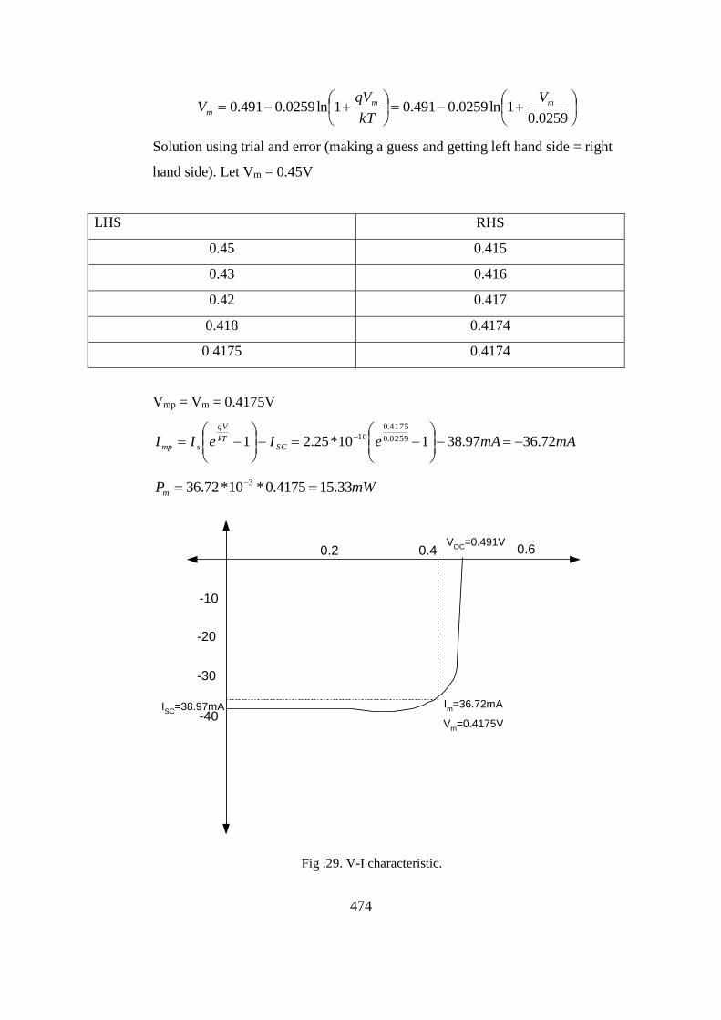
474
Solution using trial and error (making a guess and getting left hand side = right
hand side). Let Vm = 0.45V
LHS RHS
0.45 0.415
0.43 0.416
0.42 0.417
0.418 0.4174
0.4175 0.4174
Vmp = Vm = 0.4175V
Fig .29. V-I characteristic.
0259.01ln0259.0491.01ln0259.0491.0 mm
m
V
kT
qVV
SCkT
qV
smp IeII
1 mAmAe 72.3697.38110*25.2 0259.0
4175.0
10
mWPm 33.154175.0*10*72.36 3
0.2 0.4 0.6
-10
-20
-30
-40
VOC
=0.491V
Im
=36.72mA
Vm
=0.4175V
ISC
=38.97mA

475
Fill Factor (FF) =
Change of ideality factor n
From the previous examples, we can say that ‘n’ does not change fill factor.
There are some ways to obtain a fill factor of 0.9.
a. One-way is to reduce Is by increasing the doping of the substrate.
b. The other way is to use a heterojunctions. Both results in high VOC.
Reducing Is or Increasing VOC
Increase the doping of the substrate. Let ND = 100*4*1014 = 4*1016 cm-3. We will
keep NA for p+ = 1020 cm-3.
VOC value will go higher if ND is increased above 4*1016.
The new Is’ value
The new equation is,
Guess values are,
LHS RHS
0.55 0.5302
0.53 0.531
0.531 0.5311
8.097.38*491.0
33.15
mA
mW
SCnkT
qV
smp IeII
1
VI
II
q
kTV
S
SSCOC 6106.0
10*25.2
10*97.38ln0259.0ln
12
3
p
np
L
pqAD '
0
33'
0 10*625.5 cmpn
AI s
12
3
319' 10*25.2
10*5
10*625.5*5.12*10*6.1
SCkT
qV
IeI
110*25.2 12
0259.01ln0259.06106.01ln
''
'' mmOCmmp
V
kT
qV
q
kTVVV
VVm 531.0'
mAIm 16.3710*97.3810*8033.1 33'

476
Fill Factor =
Fig. 30. I-V plot for new ND = 4*1016 cm-3 shows a slight improvement.
3) Losses: Losses in a solar cell are due to:
e. Long wavelength (h < Eg of 1.1eV for Si)
f. Excess photon energy not used in generating electron-hole pairs.
g. Voltage factor (qVOC/Eg)
h. Fill Factor
Long wavelength photons are not absorbed as their energy is below the
energy gap Eg.
a. With reference to the figure 31, in area of region 1, 2 & 3, the solar power is:
b.
c. Region #1 68.4 W/m2
d. Region #2 72.69 W/m2
e. Region #3 35.77 W/m2
f.
g. Total long wavelength (h < Eg of 1.1eV for Si) photons losses= 176.86 W/m2
83.010*97.38*6106.0
10*16.37*531.03
3
0.1 0.5
-10
-20
-30
-40
VOC
=0.6106V
Im
=37.16mA
Vm
=0.531V
ISC
=38.97mA
0.3

477
Fig. 31. Two curves related to solar spectral irradiance. Fig. 32. Excess energy loss(below).

478
h. Excess photon energy for Air Mass One
Excess photon energy = h - Eg,Si
Let AM1 plot above < 1.1m or h > 1.1 eV is divided in several regions. (The
exact way is to find the area under the curve numerically)
AM1 plot above h > 1.1eV
Regions are Triangle J, Trapezoid J, Trapezoid marked as #4, small
rectangular regions #5 & #6.
J => Photon energy at =
Photon energy at J =
Excess photon energy = 3.21 – 1.1 = 2.11eV.
Area of the J =
Excess energy not used =
Trapezoid J => h at J =>
h at =>
Area = Rectangle ’J + ’
= 950*(0.84-0.51) + (0.84-0.51) * (1550-950)/2 = 412.5 W/m2
Excess energy lost = (412.5/1.953) * 0.843 = 178.05 W/m2
Trapezoid #4, Rectangle #5 & Rectangle #6 can be combined by a rectangle.
= -500 * (0.84-1.1) = 130 W/m2
Excess energy = have – Eg = 1.3 – 1.1 =0.19eV
eV431.0
24.1
eV43.251.0
24.1
eVh ave 21.32
43.24
2/1552
31.051.0*1550
2* mW
JJ
2/10111.2*21.3
155mW
eV43.271.0
24.1
eV476.184.0
24.1
eVh ave 953.12
43.2476.1
eVh ave 3.12
127.1476.1
2
1.1
24.1
84.0
24.1
479
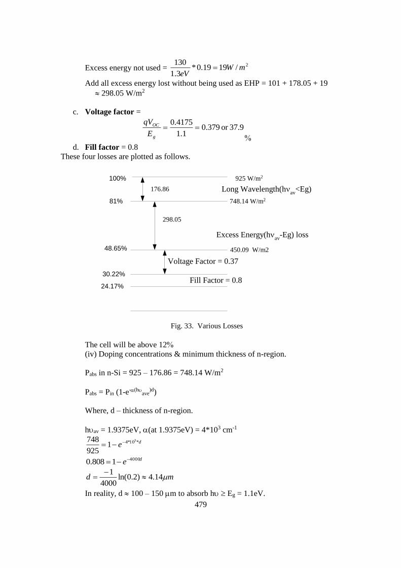
Excess energy not used =
Add all excess energy lost without being used as EHP = 101 + 178.05 + 19
298.05 W/m2
c. Voltage factor =
d. Fill factor = 0.8
These four losses are plotted as follows.
Fig. 33. Various Losses
The cell will be above 12
(iv) Doping concentrations & minimum thickness of n-region.
Pabs in n-Si = 925 – 176.86 = 748.14 W/m2
Pabs = Pin (1-e-(have
)d)
Where, d – thickness of n-region.
hav = 1.9375eV, (at 1.9375eV) = 4*103 cm-1
In reality, d 100 – 150 m to absorb h Eg = 1.1eV.
2/1919.0*3.1
130mW
eV
37.9or 379.01.1
4175.0
g
OC
E
qV
100%
81%
48.65%
30.22%
24.17%Fill Factor = 0.8
Voltage Factor = 0.37
176.86
298.05
450.09 W/m2
748.14 W/m2
925 W/m2
Excess Energy(hav
-Eg) loss
Long Wavelength(hav
<Eg)
de *10*4 3
1925
748
de 40001808.0
md 14.4)2.0ln(4000
1

480
6.8.2 Solar cell design for AM 0 (outer space)
Isc Voc as a function of Eg: See also Section 6.12.
Polynomial exponential set for Isc plot
Isc = 100-36.73(Eg-0.3019)-9.779(Eg-.03019)2+3.911(Eg-0.0319)2 (57)
Voc =kT(ln (Isc+Is)/Is)≅ (kT/q)ln (Isc/Is) (58)
=(kT/q)ln (Isc)- (kT/q)ln (Is) (59)
For a p+-n cell
Is=qADpPno/Lp+ qADnnpo/Ln
qADnnpo/Ln is small as npo<< pn0
≅ qADnnpo/LpNd(4)
≅ qADp/LpNd*4*(4∏2mnmp(kT)2)/4Ψ)3/2e-(Eg/kT)
=((1.6*10-19*10-4*12.5*10-4)/(5*10-3*10-2*10-16*10-6))* ((4∏2mnmp(kT)2)/4Ψ)3/2e-
(Eg/kT))
= 2.12*105*2e-(Eg/kT) (60)
Eqs. (60) and (57)
Voc = kT/q ln Isc-kT/q*ln(2.12*105*e-Eg/kT)
=kT/q ln Isc-kT/q ln2.12*105+Eg/q
The attached plots that Isc,Voc, Isc Voc we can see Isc Voc peaks at~ 1.4eV
ni2 = 4*(((4∏2*.0067*.62*(9.11*10-31)2*(1.38*10-23*300)2)/(6.639*10-34)4)3/2
Isc = 100 – 36.73(Eg – 0.03019) – 9.779(Eg – 0.03019)2 +3.911(Eg – 0.03019)3
Fig. 34 shows Isc as a function of Eg at Air mass m=0. See also Fig .17(b) for ISC data.

481
Fig. 34. Isc as a function of Eg (Air mass 0).
Fig. 35. Voc as a function of Eg (Air mass 0).
Voc = 0.0259ln(Isc) – 0.317 + Eg/q

482
Fig. 36. Voc x Isc as a function of Eg (Air mass 0).
Solar losses for Air Mass AM0
Fig. 37. Solar spectral irradiance air mass 0
0.2 2.62.01.40.8
200
0
2200
2000
1800
1600
1400
1200
1000
800
600
400
1.1 1.7 2.3
Wavelength (m)
Sp
ectr
al
Irra
dia
nce (
W/m
-2
m-1
)
2400
Air Mass Zero (353 W/m2)
GaAs (c = 0.87 m)
Si (c = 1.1 m)
h1.11.3
A
B
C
J
H
I
E
F
DG
1.4

483
We have divided the ABED part of the spectrum in which photons have energies greater
than 1.1eV (Si = Eg)
Let us look at DEFG trapezoid
No of photons whose power is represented by FE curve.
Excess energy / Photon =
Total excess energy lost per sec =
Similarly find the total excess energy lost per second in other trapezoids. Add then up and
you will obtain the power lost. Find the percentage power lost.
G D
E
F
average
DEFGPH
h
AreaofFEGDN
/
Si ofEh gaverage
hQ h
gaverageDEFGPH EhN *
484
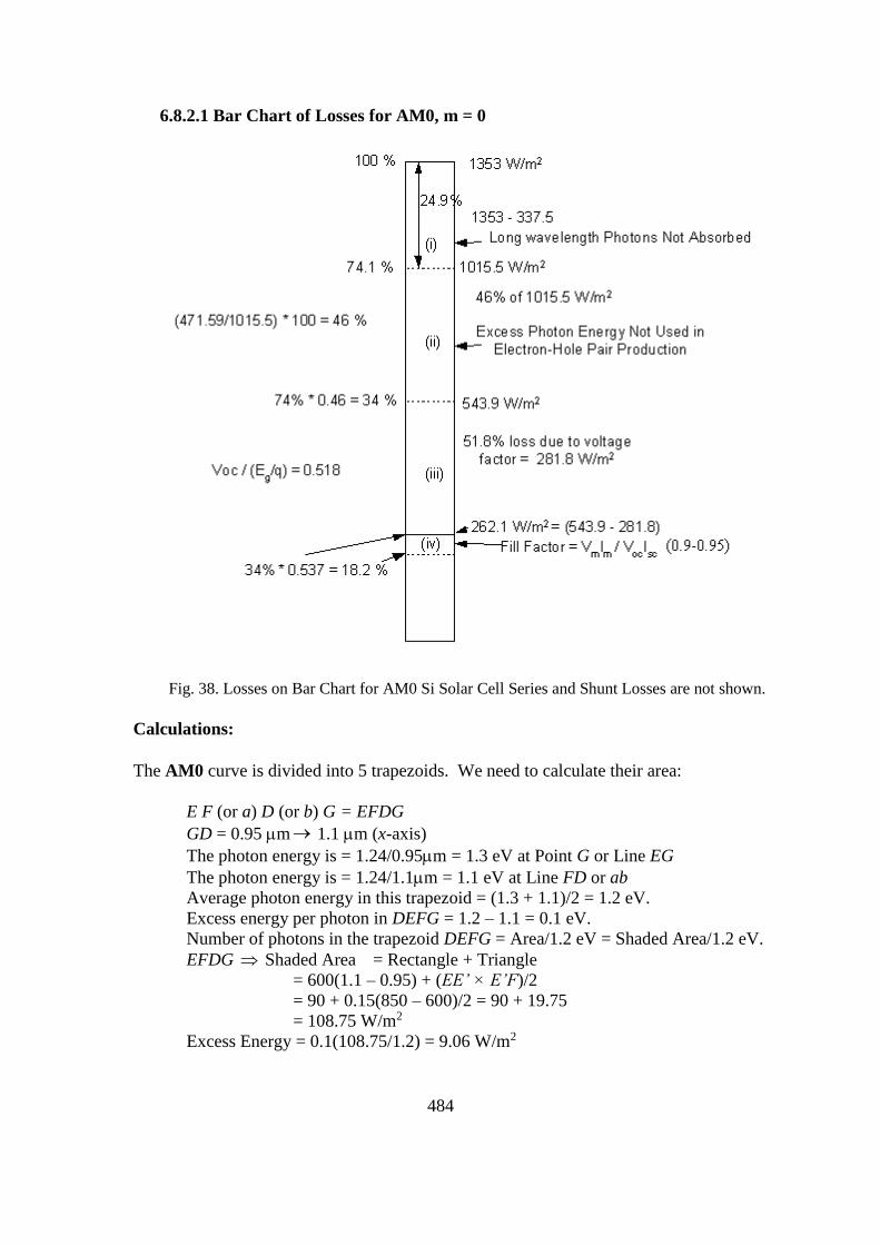
6.8.2.1 Bar Chart of Losses for AM0, m = 0
Fig. 38. Losses on Bar Chart for AM0 Si Solar Cell Series and Shunt Losses are not shown.
Calculations:
The AM0 curve is divided into 5 trapezoids. We need to calculate their area:
E F (or a) D (or b) G = EFDG
GD = 0.95 m 1.1 m (x-axis)
The photon energy is = 1.24/0.95m = 1.3 eV at Point G or Line EG
The photon energy is = 1.24/1.1m = 1.1 eV at Line FD or ab
Average photon energy in this trapezoid = (1.3 + 1.1)/2 = 1.2 eV.
Excess energy per photon in DEFG = 1.2 – 1.1 = 0.1 eV.
Number of photons in the trapezoid DEFG = Area/1.2 eV = Shaded Area/1.2 eV.
EFDG Shaded Area = Rectangle + Triangle
= 600(1.1 – 0.95) + (EE’ × E’F)/2
= 90 + 0.15(850 – 600)/2 = 90 + 19.75
= 108.75 W/m2
Excess Energy = 0.1(108.75/1.2) = 9.06 W/m2

485
HEGI Trapezoid II
HI line: value = 0.71 m; h = 1.746 eV
EG line: value = 0.95 m; h eV
Average (h photon energy = (1.746 + 1.3)/2 = 1.523 eV
Excess energy = 1.523 – 1.1 = 0.423 eV
Area of HEGI trapezoid = Rectangle H’EGI + Triangle HH’E
= 850(0.95 – 0.71) + [(1300 – 850)(0.95 – 0.71)]/2
= 204 + 54 = 258 W/m2
Excess Energy = 258(1.523 – 1.1)/1.523 = 71.65 W/m2
BJIH Trapezoid III
BJ line: value 0.51 m; h = 2.43 eV
HI line: value = 0.71 m; h eV
Average photon energy = (1.746 + 2.43)/2 = 2.088 eV
Excess energy = 2.088 – 1.1 = 0.988 eV
Area of BJIH trapezoid = Rectangle B’HIJ + Triangle BB’H
= 1300(0.71 – 0.51) + 0.2(2100 – 1300)/2
= 260 + 80 = 340 W/m2
Excess energy = 340(0.988)/2.088 = 160.88 W/m2
Triangle ABJ
Area of ABJ triangle: 2100(0.51 – 0.2)/2 = 325.5 W/m2
Average photon energy = 1.24/0.2 – 1.24/0.51 = 6.2 – 2.43 = 3.77 eV
Excess energy = 3.77 – 1.1 = 2.67 eV
Excess photon energy wasted = (325.5)(2.7)/3.77 = 230 W/m2
Total excess energy wasted = 9.06 + 71.65 + 160.88 +230 = 471.59 W/m2

486
6.9 Fabrication & Simulation of Solar Cells: Student Project Johnhenri Richardson
Advisor: Professor Facquir Jain Research Partner: Pratiba Anand
UConn Dept. of Electrical & Computer Engineering REU Summer 2006, August 2, 2006
Abstract
A single junction silicon solar cell was fabricated by phosphorus diffusion of a p-type
silicon wafer. Additionally, two-junction solar cells were modeled in MATLAB. The
fabricated solar cell had a Voc of 0.433V, a Jsc of 9.8mA/cm^2, and a fill factor of 67%. The
simulated tandem solar cell had a Voc of 1.19V, a Jsc of 18mA/cm^2, and a fill factor of 88%.
Introduction
A simple solar cell can be made by fabricating a diode whose bandage energy is near
typical photon energies in sunlight. At the earth’s surface, sunlight intensity as a function of
wavelength peaks around 650nm, or 1.9eV. This makes a silicon p-n junction, with a bandage
energy Eg of 1.1eV, a good material for solar cell fabrication. The silicon solar cell absorbs
photons with energies at or above 1.1eV, creating mobile charge carriers in the form of
electrons and holes. If connected to a circuit, the solar cell can then behave like a current source
out to some open circuit voltage limited by its material properties.
Such a silicon solar cell was fabricated in the lab. Starting with a p-type silicon wafer,
we created a p-n junction by phosphorus diffusion. The I-V characteristics of the resulting solar
cell were promising and could probably be easily improved. However, due to equipment
failure, only one solar cell could be fabricated during the program’s time frame.
Single junction solar cells have two major inefficiencies. First, all photons below the
solar cell band gap energy pass through unabsorbed. These photons do not have enough energy
to excite an electron into the conduction band, so they cannot be used to generate charge
carriers. Second, photons above the band gap energy do not impart all of their energy to the
circuit. Instead, the difference Ephoton - Eg is lost via thermal and other interactions, and only
the bandage energy is used by the solar cell.
To minimize these losses, many researchers turn to tandem solar cells. Tandem solar
cells consist of two p-n junctions stacked and connected in series. The top junction has a
relatively large band gap energy, capturing the high energy photons with minimal thermal
losses while letting low energy photons pass. The bottom junction has a lower band gap energy,
absorbing a large fraction of what the top junction lets through.
These tandem cells were modeled based on the work of Kurtz.1 Using MATLAB, the
tandem solar cell’s I-V characteristics were calculating from material properties of the solar
cell itself. The resulting data allow exploration of tandem cells and cells made from materials
other than silicon.
Solar Cell Fabrication Procedure
One solar cell was fabricated in the lab. We started with a boron-doped p-type silicon
wafer. The wafer was cleaned by a standard procedure to remove oxides from its surface. Once
prepared, the sample underwent phosphorus diffusion at 1000°C for 10 minutes. This deposited
a layer of phosphorus-doped n-type silicon on both sides of the wafer. Back-etching followed
487
diffusion. Protecting the front surface of the wafer with wax, we dipped the wafer into a slow
silicon etch solution, which removed the n-type layer from the back surface. We etched until a
thermocouple probe showed the back surface to be p-type. These steps created the needed p-n
junction.
Following diffusion, the sample underwent metallization. Thermal evaporation was
used to apply metal contacts. The back surface was covered with a layer of aluminum. The
front surface was covered with a pattern of gold-arsenic dots, each 0.51mm in diameter and
spaced 1.3mm apart. This small, tightly spaced dot pattern created complications in then next
step.
Once metal contacts had been applied, the gold-arsenic dots needed to be mesa etched.
The procedure called for each dot to be covered with wax, then a slow silicon etch to be applied
to the top surface. This would leave only a ring of n-type silicon around each dot, minimizing
leakage currents flowing between contacts. However, because the dots were so closely spaced,
applying wax to individual dots proved extremely difficult. When the mesa etching procedure
was complete, many gold-arsenic contacts had either been lost or were still connected to other
contacts by n-type silicon. This made measured results from the solar cell very inconsistent
from dot to dot. Nevertheless, some contacts were properly etched and gave good results.
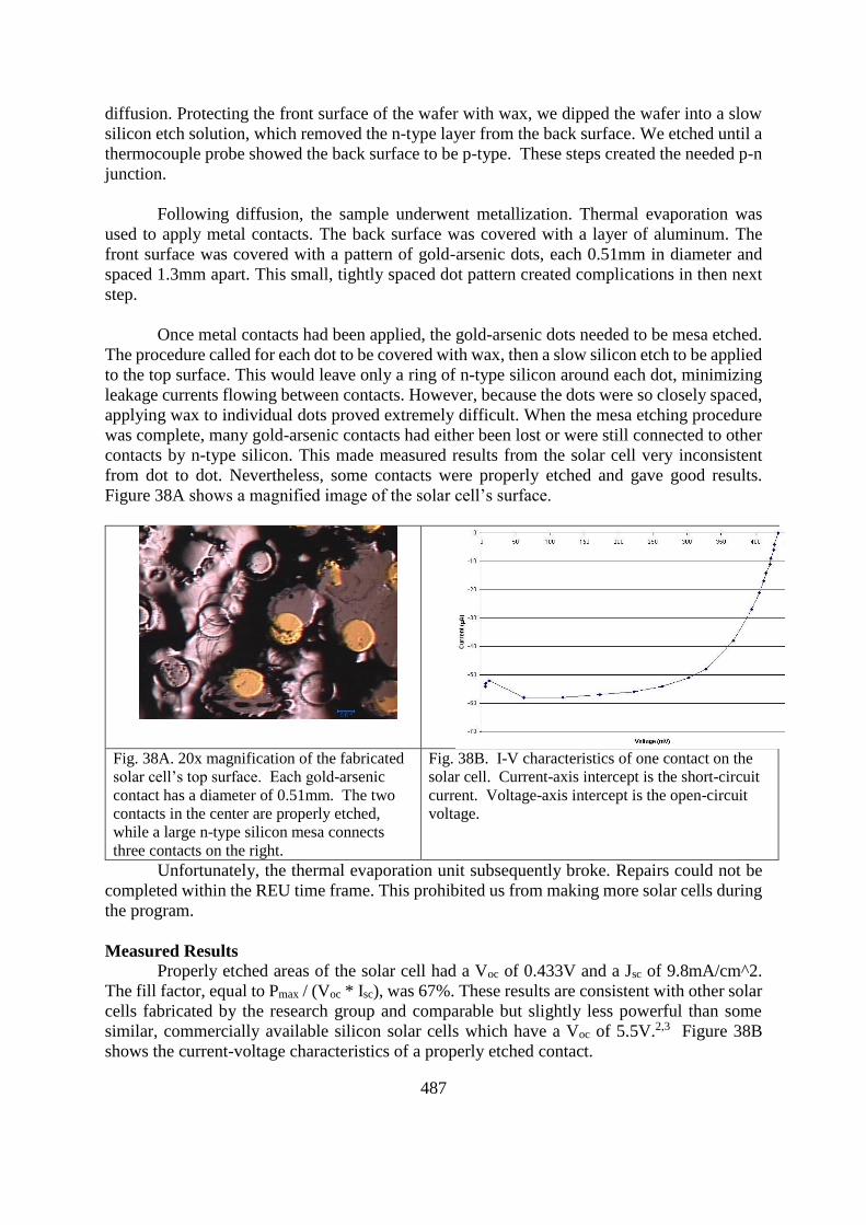
Figure 38A shows a magnified image of the solar cell’s surface.
Fig. 38A. 20x magnification of the fabricated
solar cell’s top surface. Each gold-arsenic
contact has a diameter of 0.51mm. The two
contacts in the center are properly etched,
while a large n-type silicon mesa connects
three contacts on the right.
Fig. 38B. I-V characteristics of one contact on the
solar cell. Current-axis intercept is the short-circuit
current. Voltage-axis intercept is the open-circuit
voltage.
Unfortunately, the thermal evaporation unit subsequently broke. Repairs could not be
completed within the REU time frame. This prohibited us from making more solar cells during
the program.
Measured Results
Properly etched areas of the solar cell had a Voc of 0.433V and a Jsc of 9.8mA/cm^2.
The fill factor, equal to Pmax / (Voc * Isc), was 67%. These results are consistent with other solar
cells fabricated by the research group and comparable but slightly less powerful than some
similar, commercially available silicon solar cells which have a Voc of 5.5V.2,3 Figure 38B
shows the current-voltage characteristics of a properly etched contact.
488
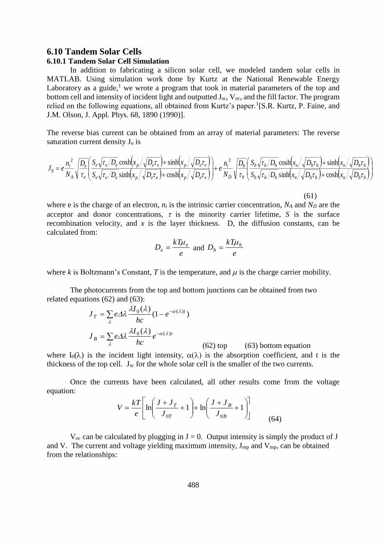
6.10 Tandem Solar Cells 6.10.1 Tandem Solar Cell Simulation
In addition to fabricating a silicon solar cell, we modeled tandem solar cells in
MATLAB. Using simulation work done by Kurtz at the National Renewable Energy
Laboratory as a guide,1 we wrote a program that took in material parameters of the top and
bottom cell and intensity of incident light and outputted Jsc, Voc, and the fill factor. The program
relied on the following equations, all obtained from Kurtz’s paper.1[S.R. Kurtz, P. Faine, and
J.M. Olson, J. Appl. Phys. 68, 1890 (1990)].
The reverse bias current can be obtained from an array of material parameters: The reverse
saturation current density Jo is
(61)
where e is the charge of an electron, ni is the intrinsic carrier concentration, NA and ND are the
acceptor and donor concentrations, is the minority carrier lifetime, S is the surface
recombination velocity, and x is the layer thickness. D, the diffusion constants, can be
calculated from:
and
where k is Boltzmann’s Constant, T is the temperature, and is the charge carrier mobility.
The photocurrents from the top and bottom junctions can be obtained from two
related equations (62) and (63):
(62) top (63) bottom equation
where I0() is the incident light intensity, is the absorption coefficient, and t is the
thickness of the top cell. Jsc for the whole solar cell is the smaller of the two currents.
Once the currents have been calculated, all other results come from the voltage
equation:
(64)
Voc can be calculated by plugging in J = 0. Output intensity is simply the product of J
and V. The current and voltage yielding maximum intensity, Jmp and Vmp, can be obtained
from the relationships:
hhnhhnhhh
hhnhhnhhh
h
h
D
i
eepeepeee
eepeepeee
e
e
A
i
DxDxDS
DxDxDSD
N
ne
DxDxDS
DxDxDSD
N
neJ
coshsinh
sinhcosh
coshsinh
sinhcosh 22
0
e
kTD e
e
e
kTD h
h
tB
tT
ehc
IeJ
ehc
IeJ
)(0
)(0
)(
)1()(
1ln1ln
00 B
B
T
T
J
JJ
J
JJ
e
kTV

489
and (65)
The fill factor can then be calculated as a ratio of intensities: .Using these
equations, all relevant solar cell measurements can be simulated.
Simulation Results
Using the equations above, tandem solar cells were simulated using top cell thickness
as the independent variable. The thickness was varied from 10m to 100m. Incident sunlight
intensities, silicon absorption coefficients, and silicon material parameters were obtained from
course lecture notes used by Professor Jain.4 As the top solar cell thickness increased, Voc, Jsc,
and Pmax decreased and the fill factor grew as the additive inverse of Pmax with a plateau at 89%.
Figure 38C shows Pmax as a function of the top cell thickness. At a top cell thickness of 20m,
Voc = 1.19V, Jsc = 18 mA/cm2, and the fill factor was 88%.
Fig. 38C. Output intensity vs. top cell thickness.
Conclusion
The results of the fabricated solar cell were acceptable but left a lot of room for
improvement. Had we been able to make more cells, we probably would have seen slight
improvement in the open circuit voltage and short circuit current. We would also have used a
more convenient top metal contact pattern. This would improve consistency of the results
across the entire surface of the solar cell.
The simulation results were very reasonable but seemed a bit optimistic. The equations
used probably ignore a number of losses that arise during actual fabrication of the solar cells.
This gives slightly higher output intensities and fill factors than we would expect to see in the
lab. However, the simulation still gave reasonable results and showed how those results varied
for different material properties, such as top cell thickness. The program also allows simulation
of semiconductors other than silicon, since the user can input properties of different materials.
This flexibility permits the research group to explore both tandem solar cells and solar cells
made from materials other than silicon.
References1S.R. Kurtz, P. Faine, and J.M. Olson, J. Appl. Phys. 68, 1890 (1990). 2Radio Shack Silicon Solar Cell, Catalog#276-124; http://www.radioshack.com/home/index.jsp
0dJ
dP)( mpmp JVV
scoc JV
PFF max
0
5
10
15
20
25
10 30 50 70 90
Top Solar Cell Thickness (m)
Inte
nsit
y (
mW
/cm
^2)

490
3Silicon Solar Inc. Solar Cell, Catalog #: 04-1193. http://www.siliconsolar.com/#skusearcha 4F. Jain, ECE 245 Supplementary Notes (2006).
6.10.2 Tandem Solar cells using amorphous and crystalline cells
Figure 39 shows a typical tandem cell with amorphous and crystalline solar cells.
Fig. 39. Structure of Tandem solar cell.
The overall voltage current relations are provided below:
Equation 1 shows the total voltage which is a series combination of two voltages in the top
and the bottom cell.
V=VT + VB (66)
The voltage drop across the top and bottom cells are given by
(67)
Alternately, this equation can be written in terms of currents rather than current density J.
(68)
Equation 2B uses the individual solar cell current-voltage equation, which are
expressed below. For the top cell the current is dependent on its reverse saturation current IST
and photon generated current ISCT.
Tunnel Junction
N Amorphous Si,
NDT
P Amorphous
Si, NAT
N Si, NDB
P Si, NAB
Top Ohmic
Contact
Bottom Ohmic Contact
0.015µm
0.5µm
0.5µm
10µm
Top
Amorphous
Si cell
Bottom
Si cell
Homojunction # 1
Top cell
P+ AmorphousSi
n+ Si layer
Current density
J or current I
+
_
Load V
Photons
between
1.5-1.1eV
Photons
greater
than 1.5eV n1
p1
n2
p2
1ln1ln
SB
SCB
ST
SCT
J
JJ
J
JJ
q
kTV
1ln1ln
SB
SCB
ST
SCT
I
II
I
II
q
kTV

491
Eq. 69
Similarly, the bottom cell current is dependent on its voltage VB and short circuit current ISCB.
Eq.70
Here, the reverse saturation current density Js is expressed as:
For the top cell:
JsT= q [(DnT npoT/LnT) + (DpT pnoT/LpT)] (71)
For the bottom cell:
JsB= q [(DnB npoB/LnB) + (DpB pnoB/LpB)] (72)
Because of the finite lengths of the absorbing regions p1 and p2, the boundary
conditions are different and the exact expressions of the reverse saturation current density is
modified [see Section 6.13 ] as Eq.73 below:
𝐽𝑠 = 𝑞𝑛𝑖
2
𝑁𝐴 √
𝐷𝑒
𝜏𝑒(
𝑆𝑒√𝜏𝑒/𝐷𝑒𝑐𝑜𝑠ℎ𝑥(𝑥𝑝/√𝐷𝑒𝜏𝑒) + sinh (𝑥𝑝/√𝐷𝑒𝜏𝑒)
𝑆𝑒√𝜏𝑒/𝐷𝑒𝑠𝑖𝑛ℎ𝑥(𝑥𝑝/√𝐷𝑒𝜏𝑒) + cosh (𝑥𝑝/√𝐷𝑒𝜏𝑒))
+ 𝑞𝑛𝑖
2
𝑁𝐷√
𝐷ℎ
𝜏ℎ(
𝑆𝑒√𝜏𝑒/𝐷𝑒𝑐𝑜𝑠ℎ𝑥(𝑥𝑝/√𝐷𝑒𝜏𝑒) + sinh (𝑥𝑝/√𝐷𝑒𝜏𝑒)
𝑆𝑒√𝜏𝑒/𝐷𝑒𝑠𝑖𝑛ℎ𝑥(𝑥𝑝/√𝐷𝑒𝜏𝑒) + cosh (𝑥𝑝/√𝐷𝑒𝜏𝑒)) (73)
Eq. 73 can be recognized as Eq. 61, if we substitute npo= ni2/NA and Dn/Ln = (Dnn)
1/2.
Here, ni is the intrinsic carrier concentration, NA and ND are the acceptor and donor
concentrations, is the minority carrier lifetime, S is the surface recombination velocity, and x
is the layer thickness. D, the diffusion constants, can be calculated from:
and (74)
where k is Boltzmann’s Constant, T is the temperature, and is the charge carrier mobility.
The short circuit current densities for the top and bottom cells are expressed in Eqs. 66 as:
(75A)
(75B)
where I0() is the incident light intensity as a function of wavelength, h is Planck’s constant, c
is velocity of light, andare the absorption coefficient in top and bottom layers,
respectively, and tpT, tT and tpB are the thicknesses of p-absorbing layer (top cell), total thickness
of top cell, and p-absorbing layer of the bottom cell, respectively. Also, k is the Boltzmann
e
kTD e
e
e
kTD h
h
SCTT
ST IkT
qVII
]1[exp*
SCBB
SB IkT
qVII
]1[exp*
pBBBTT
pTT
tt
SCB
t
SCT
eehc
IqJ
ehc
IqJ
1)/(
)(
)1()/(
)(
)(0
)(0

492
constant, and T the temperature.
The short circuit current of the cell was taken as the lesser of JSCT and JSCB. The open
circuit voltage is calculated by substituting current density J to be zero.
(67)
(76)
Power output per unit area is simply the product of J and V. The maximum output
current density Jmp and voltage Vmp can be obtained using:
.
The fill factor can then be calculated as:
(77)
Using these equations, all relevant solar cell measurements can be simulated.
Results: Single crystalline Si-Solar cell
Thickness Is Isc Voc
tn = 0.5 m,tp = 10 m 7.1752* 10-13 A 0.0456 A 0.6702 V
Fig. 40 I-V Characteristic of Si solar cell.
Single Amorphous Si-Solar cell
Thickness Is Isc Voc
tn = 0.015 m
tp = 0.5 m
2.59* 10-13 A 0.0030 A 0.6256 V
1ln1ln
SB
SCB
ST
SCT
J
JJ
J
JJ
q
kTV
1ln1ln
SB
SCB
ST
SCToc
J
J
J
J
q
kTV
0dJ
dP
scoc JV
PFF max

493
Fig. 41 IV characteristic of Amorphous Si solar cell.
Tandem Solar cell
Thickness Reverse
Saturation
Short circuit
current
density
Tandem
Voc
Max current
density
Jmp
Max output
Vmp
Fill
Factor %
Amorphous Si
(Top) =tT=0.515m
Crystalline Si
(Bottom)
tB= 10.5 m
JST = 2.5923*
10-13 A/cm2
JSB = 7.1752*
10-13 A/cm2
JSCT = 0.0074
A/cm2
JSCB =
0.034A/cm2
For series, we
pick
Jsc =
0.0034A/cm2
1.1989 V 0.0033
A cm-2
1.0866 V 88.5
Tandem solar cell comprising of Amorphous Si and Crystalline Si cell:
Fig. 42 shows the Voltage Current characteristic of the tandem cell. This cell is similar ato
the cell shown in Fig. 44 Sanyo’s Heterojunction with intrinsic thin film (HIT) cell.

494
Fig. 42 I-V characteristic of the tandem solar cell.
6.11 Tandem, MEG, and Quantum Dot Solar Cells: Part-II
6.11.1 Emerging new cell structures:
Next we describe cells which have emerged during last 10 years. These include:
1. Sanyo’s heterojunction with intrinsic thin film (HIT) cell and amorphous Si
window and crystalline Si cell
2. CdTe-CdS cells as commercialized by First Solar Corp.
3. Intermediate Band (IB) Cell: these cells have not been demonstrated.
4. Multiple exciton generation (MEG) cells
5. 4-5 junction tandem cells
6. Organic and polymer cells
7. Quantum dot and quantum wire cells.
6.11.1.1 Fundamentals of Optical Transitions: We need to go over excitonic transitions
before we discuss the new technologies. There are two processes involving photons.
1. Emitting Photons, and
2. Absorbing Photons. The absorption involves transitions involving
a. Excitonic Transitions
b. Free Carrier Transitions
i. Intra band [Within sub bands of well or wire (semiconductors)]
Within valance or conductor (metals)
ii. Inter-band like Valance band to Conduction band
Excitonic transitions take place when not enough energy is given by a photon to get an
electron from the valence band to conduction band or generate an electron and hole pair.
Exciton Binding Energy Eex is related hv= Eg - Eex
hv ≥ Eg hv-Eg =excess energy

495
3. Absorption of photons is relevant not only to solar cells as well as optical
modulators.
We next briefly describe the operation of optical modulators using the above effects..
Optical Modulators: In the case of modulators we harness absorption of photons and
variation of absorption as a funciton of applied external voltage or electric field.
a. Electroabsorption [change in α(Ep)] is used in photodetectors and Optical
modulator
b. Electrorefraction refers to change in the index of refraction nr
(perpendicular electric field) due to an externally applied perpendicular
electric field
Intensity Modulation: Intensity changes due to change in the absorption coefficient
for a travel of distance x in the medium.
I=Ioe-(E) x ⇒ Index of refraction is function of applied field
Phase Modulation: Changes in phase nras light travels in a
medium L due to change in index of refraction nr.
If the Fabry-Perot cavity is made of a medium whose phase can be changed by
applying electric field, we can obtain intensity modulation.
Field-Dependent Birefringence: Polarization of light is function of applied field in
liquid cyrstal displays (LCDs) and multiple quantum wells (MQWs).
Intensity modulation can be obtained if we sandwich a field-dependent birefringent
material between two cross polarizers.
In metals and certain quantum wells/wires structure we observe intra band transitions.
Absorption in quantum well, wires and dots: Photon absorption coefficient increases as we
go from wells to wires and to quantum dots.
Absorption coefficient is related to index of refraction change by Kramer Kronig
relations. Once we know the absorption spectrum , we can find the index of refraction
and changes in its value.
Excitonic Transitions: Quantum Confined Stark Effect in MQWs: Shift of photon
absorption to lower energy is called Stark effect. It involves red shift. See appendix.
Stark effect is used in electroabsorptive modulators using wells, wires and dots.
496
Solar cells: Photon absorption creates e-h pairs in semiconductors. More pairs with
increasing intensity of light. Inter-band absorption is most dominant pathway to absorb
photons. Inter-band absorption is of two types:
1. Direct transitions involving no phonons (see the expression for in Section 6.3)
2. Indirect transitions involving phonons.
Excitonic transitions and multiple exciton generation (MEG) is another recent method to
absorb photons with smaller excess energy loss.
6.11.1.2 Nanostructures in Solar Cells and Current Technologies
Nanostructures are utilized either as wavelength independent absorption layer to minimize
reflection on the solar cells as highly absorbing compact layers forming junction(s)
incorporating quantum dots or wires/tubes.
Solar Cells and Modules: Solar cells can be divided into three broad categories:
1. Inorganic Semiconductor – based solar cells
2. Organic Semiconductor (OSC)- based solar cells
3. Inorganic-Organic hybrid cells
We will primarily focus on inorganic solar cells. Organic Photovoltaics (OPVs) are
briefly discussed at the end of this write up. The material presented here is primarily based on
two monthly volumes of MRS Bulletins (January 2005, and March 2007).
Solar cells are deployed as modules. Modules production and processing depends on
the type of solar cells. It is critical in estimating the cost of energy generation. The chart below
shows the cost of Si based modules (both thin film Si and Si wafers). This has given a
benchmark for other technologies.

497
Fig. 43. Module price as a function of power production.
R. M. Margois, NCVP Solar Program Review Meeting, Denver, CO, 2003.
Ref. S. E. Shaheen et al., Organic based photovoltaics: Toward low-cost power generation, MRS
Bull., p.10, January 2005.
Inorganic solar cells are divided into following categories:
1. Si based cells: (these are also referred to as First Generation). Some of the Si cells,
particularly those including tandem amorphous and microcrystalline cells could be
called 2nd or 3rd generation).
These include Si cells with varying morphology:
Material morphology Conversion efficiency
Single Crystal (SC) Si 24.7% cells,
22.7% modules
Multi-Crystalline Si (mc-Si) or nanocrystalline (nc) 20.3% cells,
15.3% modules
Si Ribbons
2. Thin Films Solar Cells: (also called second generation cells).
Under this category, we will present Si cells and non-Si cells.
(a) Amorphous hydrogenated Si:H and SiGe:H cells are fabricated in two forms. Amorphous-Si:H has an energy gap of 1.7-1.9eV. This means these cells will produce
higher open circuit voltage. However, the photocurrent is smaller due to insufficient
absorption of sun light.

498
Tandem a-Si:H/a-SiGe:H/a-SiGe: H cells have demonstrated very high efficiency.
Some examples are given below: (R. Schropp et al., MRS Bull., p.219, March 2007).
Table: Amorphous and Poly-crystalline/Micro or nanocrystalline cells
Material Efficiency #of Junctions Company
a-Si/a-SiGe/nc-Si:H 15.07% 3 United
Solar Ovonic
c-Si:H 10.3% 1 IPV Julich
SPC Poly-Si 9.8% 1 CSG Solar
(SPC=Solid phase crystallization; AlC=Aluminun induced crystallization)
6.11.2 Heterojunction with intrinsic thin film (HIT) cell
(Ref: M. Tanaka et al, Photovoltaic Energy Conversion, Proc. 3rd word Conf, 1, p.955, 2003.
It consists of c-Si layer with a-Si (p-n) junction on top (having transparent conducting oxide
TCO and a metallic collection grid contact). HIT cell based modules have reported an
efficiency of 19.3% by Sanyo.
Fig. 44 Sanyo’s
Heterojunction with intrinsic
thin film (HIT) cell.
(a) cSi-aSi-TCO-Metal grid
contact HIT n-aSiH/a-
n+Si/p-type Si wafer.
(b) Glass/TCO(bottom
contact)/p-cSi (30nm)/i-
cSi(1m)/n-aSi
(40nm)/ZnO/Ag/Al
TCO= Transparent
conducting oxides serving as
contact. tin oxide, indium
tin oxide, ZnO.
Fig. 45. Module cost /Wp in 2005. [Ref: A. Slaoui and R. Collins, p. 211, MRS Bull, March 07].
The goal here is to obtain $1.82 to $1.2/Wp in 2010 and 2015, respectively.

499
6.11.3 Thin film CdSe and CuInSe2 cells
Ref: J. Beach and B. McCandless (p.225, March 2007 MRS Bull). This
category includes cells made out of II-VI and chalcopyrite. Typical cells are:
Copper Indium diselenide (CIS), 2.CdTe, and 3. Cu(InGa)Se2 (CIGS) CdTe-
CuInSe2 cells are sensitive to moisture. Glass sheets are used to seal front and
back and polymers are used to seal the edges and bond glass. For AM 1.5
Solar Spectrum is: see http://rredc.nrel.gov/solar/spectra/am1.5/
Fig. 46. Solar spectrum under AM1.5 (To convert nanometers to µm, divide by 1000. To convert
W/sm/nm to W/sm/µm, multiply by 1000.)
First Solar disclosed cost of CdTe/CdS cell for a 25MW peak/year (MWp/year)
was $1.59/Wp. This is based on a module efficiency of 9%.
Cost goals: The DOE goal Solar America Initiative aims at $0.15 per kWh, and
system cost of $2/Wp by 2015. This generally means that the module cost should
be $1/Wp.
Lower Generation Cost/Watt requires:
Higher cell conversion efficiency
Cell efficiency resulting in module efficiency and module cost
High Throughput <-> Reduced manufacturing cost and system cost
p-CdTe/n-CdS cells are η= 16.5%. The alternative being studied includes a-
CdSxOy cells. Doping of CdTe is due to vacancies. CdTe becomes n type with
Te vacancies and p type with Cd vacancies.
Deposition of CdTe is followed by processing including annealing at temperature
T> 4000C in the presence of (CdCl2 + Oxygen) which gives optimal efficiency.
CdTe films grown at low temperature becomes recrystallized during this step.
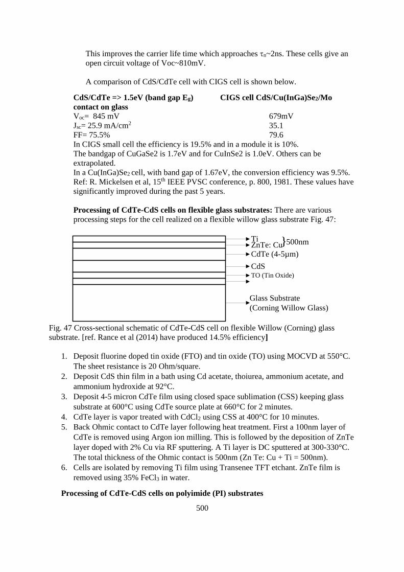
500
This improves the carrier life time which approaches n~2ns. These cells give an
open circuit voltage of Voc~810mV.
A comparison of CdS/CdTe cell with CIGS cell is shown below.
CdS/CdTe => 1.5eV (band gap Eg) CIGS cell CdS/Cu(InGa)Se2/Mo
contact on glass
Voc= 845 mV 679mV
Jsc= 25.9 mA/cm2 35.1
FF= 75.5% 79.6
In CIGS small cell the efficiency is 19.5% and in a module it is 10%.
The bandgap of CuGaSe2 is 1.7eV and for CuInSe2 is 1.0eV. Others can be
extrapolated.
In a Cu(InGa)Se2 cell, with band gap of 1.67eV, the conversion efficiency was 9.5%.
Ref: R. Mickelsen et al, 15th IEEE PVSC conference, p. 800, 1981. These values have
significantly improved during the past 5 years.
Processing of CdTe-CdS cells on flexible glass substrates: There are various
processing steps for the cell realized on a flexible willow glass substrate Fig. 47:
TiZnTe: CuCdTe (4-5µm)
CdSTO (Tin Oxide)
}500nm
Glass Substrate
(Corning Willow Glass)
Fig. 47 Cross-sectional schematic of CdTe-CdS cell on flexible Willow (Corning) glass
substrate. [ref. Rance et al (2014) have produced 14.5% efficiency]
1. Deposit fluorine doped tin oxide (FTO) and tin oxide (TO) using MOCVD at 550°C.
The sheet resistance is 20 Ohm/square.
2. Deposit CdS thin film in a bath using Cd acetate, thoiurea, ammonium acetate, and
ammonium hydroxide at 92°C.
3. Deposit 4-5 micron CdTe film using closed space sublimation (CSS) keeping glass
substrate at 600°C using CdTe source plate at 660°C for 2 minutes.
4. CdTe layer is vapor treated with CdCl2 using CSS at 400°C for 10 minutes.
5. Back Ohmic contact to CdTe layer following heat treatment. First a 100nm layer of
CdTe is removed using Argon ion milling. This is followed by the deposition of ZnTe
layer doped with 2% Cu via RF sputtering. A Ti layer is DC sputtered at 300-330°C.
The total thickness of the Ohmic contact is 500nm (Zn Te: Cu + Ti = 500nm).
6. Cells are isolated by removing Ti film using Transenee TFT etchant. ZnTe film is
removed using 35% FeCl3 in water.
Processing of CdTe-CdS cells on polyimide (PI) substrates

501
The UPILEX polyimide sheet 7.5 micron in thickness was deposited with transparent
conductive oxide (TCO) including tin doped indium tin oxide (ITO) and aluminum doped
ITO. A layer of ZnO is deposited to enhance the reproducibility of the process of solar cell
fabrication. The ITO and intrinsic ZnO are deposited by rf-sputtering at 300°C. CdS thin
film is deposited using high vacuum thermal evaporation at 165°C. This is followed by
CdTe evaporation at 350°C.
A layer of CdCl2 is thermally evaporated (20-640nm) on the CdTe surface and annealed at
420°C for 20 minutes. After the etching of CdTe top layer using bromine and methanol
solution, topcontacts of Cu/Au or pentacene/metal were deposited.
A conversion efficiency of 10% under AM1.5 conditions was reported for the polyimide
cells FF=0.678, Jsc = 18.2 mA/cm2, Voc= 813 mV. The results were better (12%
efficiency) for soda lime glass (SLG) substrate.
CdCl2 deposition &
Anneal at 420°C
CdTe 350°C
75µm
Polyimide in Superstate UPILEX
Au
Pentacene high
work function
Tin doped ITOAl doped ITO
ZnO
TCO
Fig. 48 CdS-CdTe cell on flexible polyimide thin film.
Ref. Perrenoud, S. Buecheler, A.N. Tiwari, “Flexible CdTe Solar Cells with High
Photovoltaic Conversion Efficiency”, 2009 IEEE Conference, p.695-699, 2009.
Question: Why Voc/Eg ratio is reduced in cells having absorber semiconductor band gap
greater than 1.3eV.
A typical CdInGaSe2 (CIGS) cell is fabricated on a Molybdenum (Mo) coated soda lime
glass substrate. Over the Mo layer an absorbing layer of CIGS is deposited. This is followed
by the deposition of n-CdS. N-CdS is treated in various proprietary ways to improve the cell
characteristics. Finally transparent conducing oxides are grown. In the CIGS reported above,
ZnO and ITO conducting transparent oxides were deposited.
6.11.4 Multi-junction or Tandem Solar Cell 3rd Generation
(Ref: Dimroth and S. Kurtz, MRS Bull, March 2007, p. 230). These cells have multiple p-n
homo or heterojunctions in series, separated by one or more tunnel junctions. Expensive single
crystal substrates are used and these cells are generally operated under concentrated sun light
conditions. One sun is 1kw/m2. See Figure 49 which shows top and bottom cells connected by
a tunnel junction. (Ref: R.A Metzger, Manufacturing III-V Solar cells for space Application,
page 25, Compound Semiconductor November / December 1996).

502
Fig. 49 Cross-section of a two junction tandem cell (S. Kurtz et al., NREL). Same as Fig. 1.
Other triple junction cells are shown below. The key is to absorb part of the photons in an energy
band gap descending order. Start with a wider Eg and go to lowest Eg. Ge is lowest at 0.67eV.
F.Dimroth and S. Kurtz (p.230, MRS Bull., March 2007) have shown this in three figures
below. Fig. 50 Energy gap as a function of lattice constant in various semiconductors.
Fig. 50 Energy
gap as a
function of
lattice constant
in various
semiconductors.
GaAs Substrate Zn-doped
GaInP 0.07um p=3*10^17 cm-3 [Zn]
GaAs 3.5um p=8*10^16 cm-3 [Zn]
GaAs 0.1um n=1*10^18 cm-3 [Se]
GaInP 0.1um n=1*10^18 cm-3 [Se]
GaAs 0.01um n=1*10^19 cm-3 [Se]
GaAs 0.01um p=8*10^19 cm-3 [C]
GaInP 0.6um p=1.5*10^17 cm-3 [Zn]
GaInP 0.1um n=2*10^18 cm-3 [Se]
AlInP 0.025um n=4*10^17 cm-3 [Si]
GaAs 0.5um
n=6*10^18cm-3 [se]
Au
3um AR Coat (2 layer)
Front Grids
Contacting layers
(Eg=1.86ev)
Back Contact
Top Cell
Tunnel
Cell
Bottom Cell
GaInP/GaAs Tandem Cell

503
The absorption in various semiconductors for AM1.5 is shown below in Fig. 51..
Fig. 51 (a) Energy used by a single junction Si cell under AM1.5. Fig. 51 (b) Energy used by a
single junction Ge, GaInAs (Eg=1.18eV) and GaInP (1.7eV) cells under AM1.5 conditions.
Figure 52 shows the theoretical efficiencies for various systems. (d) and (e) show
mismatched systems using metamorphic layer (dark layer).
Fig. 52. Various material systems on Ge substrates.
Reported dual Junction GaInP/GaAs cell is 39% under 240 suns. The material is
Ga0.5In0.5As (1.7eV)/Ga0.9In0.01As(1.18eV)/Ge (0.67eV) substrate.
Single Junction Double Triple Sun Concentration (X)
% 25% 29% 31% 1
31% 39% 240
Ref: F. Dimroth, Phys. Status Solidi, 3, (3) p.373 (2006).

504
The offset [(Eg/e) – Voc] is an indicator of nonradiative losses in multi-junction
solar cells. Some values of this offset are given below.
Table Loss due to Offset Voltage [Voc/(Eg/q)]
Semiconductor Band gap (eV) Offset Volt [(Eg/q) – Voc]
GaAs 1.44 0.387
Ga0.83In0.17As 1.118 0.390
GaInNAs 1.07 0.600
Ref:R. King et al., 20th Proc. Ear. Photovol. Solar Energy Conf., p118, 2005 (Barcelona,
Spain).
Companies involved in the development are: Spectra Lab, Emcore, AZUR Space
Solar Power, and others.
Device Structure for a Triple Junction Cell (structure e): This cell (shown
below) produced a conversion efficiency of 37.9% at 10 Suns and 40% is
expected for higher concentrations. Ref: A. Bett. et al., Proc. WCPEC-4
(Waikoloa, Hawaii) 2006, p.729.
External Quantum efficiency (EQE) is a measure of carrier collection efficiency
of P-N junction. Lattice-matched and mismatched materials are used in double
and triple junction cells. Some examples are given below. In the case of
mismatched materials, metamorphic scheme is employed.
Projected conversion efficiencies are for various 3rd generation cells:
I. 66% Three-junction tandem cells
40-50% in some Multi-junction or Tandem Cells
II 66% Quantum Dot solar cells using Multi-Exciton generation (MEG)
III. Intermediate band (IB) devices.
IV. Si nanowire solar cells.
6.11.5 Multiple exciton generation (MEG), IB cells, and Quantum Dot based solar cells
When the photon energy h is greater than the bandgap, the electron and hole
generated have excess energy (h-Eg) that is given up as phonons eventually heating up
the lattice. That is, the energy of the hot carriers is lost.
Excess energy can be recovered in following ways: (a)recover hot carriers
before they thermalize (ref 2-4), and (b) hot carriers producing 2-4 electron hole pair
via impact ionization or via multiple exciton generation. Multiple exciton generation
(MEG, this is shown in QDs of PbSe, CdSe etc.)
Impact Ionization
a. 1 Photon creates 2 electron-hole pairs or exciton pairs. This is known as MEG.
b. A new possible mechanism for MEG involves simultaneous creation of
multiple excitons.

505
No group has yet reported enhanced photo carriers in the external circuit.
Quantum Yield in 300%. 3 Exciton are released.
Types of QD cells:
1. Photo electrodes composed of QD arrays,
2. QDs such as InP, 3-5nm used to sensitize a TiO2 (30nm) nanocrystalline film, and
3. QDs dispersed in organic semiconductors in blend of electron and hole
transporting polymers.
Additional details in following three pages.
New Mechanisms: use of QDs
Problem: Loss of Hot Carrier Energy (h-Eg)
1. MEG Multiple Exciton Generation: A new method to recover hot carrier energy.
(in quantum dots)
Excess Energy:
Recover Hot carriers before they Thermalize (ref-2-4).
Hot Carriers Producing 2-4 Electron Hole Pairs.
QDs: PbSe, PbS, Pbte, CdSe
Quantum Dot diameter Effective Eg
PbSe 5-7 nm 0.73 eV
4-7 nm 0.82
3.9 nm 0.91
h/Eg = 4.0
Impact Ionization
a. 1 Photon creates 2 electron–hole pairs. This is known as MEG. The electron-
hole pair when bound is called exciton. In low dielectric constant materials
excitons form readily.
b. A new possible mechanism for MEG involves simultaneous creation of multiple
excitons.

506
Fig. 53 Quantum yield is 300% if 3 excitons are formed.
No group has yet reported enhanced photocurrent in an external circuit due to this
MEG effect.
2. Intermediate Band (IB): IB cells reduce the loss of below band gap and sub-band
gap photons. Here an intermediate level is introduced by introducing a deep impurity
level in the band gap. This is shown theoretically to be useful for single junction as
well as tandem cells. Quantum efficiencies between 1 (or 100%) and 2 are predicted.
Ref. A. Luque et al, Phys. Rev. Lett. 78, p. 5014 (1997).
Fig. 52 shows Intermediate band (due to impurity level or levels; superlattice mini-
bands, lone pair bands) in the middle of CB and VB.
Fig. 54. Intermediate band schematic.
IB cells reduce loss due to long wavelength photons. See also Fig. 60.
3. Types of Quantum Dot based Cells

507
a) Photoelectrodes composed of QD arrays.
b) QDs (such as InP, 3-5nm dia) used to sensitize a TiO2 nanocrystalline film.
c) QDs dispersed in Organic/polymeric Semiconductors [i.e. in blend of electron and
hole transporting polymers].
1. Photoelectrodes composed of QD arrays
Fig. 55. 3-D Analog of mini-bands found in superlattices.
2. TCO (transparent conducing oxide) deposited with InP-sensitized TiO2 (30nm)
qc
e
h
n nn
n n
nn n
nTCO Poly
mer
Vout
4.1eV
Eg
Hole Transporting
Polymer 1.8eV-2.6eV
QD
InP
Microsphere
TiO2
q
Hole
Vacuum level
InP qc
Incident
photons
+-Incident
photons
Fig. 56. TiO2 microspheres functionalized with InP quantum dots with a hole transporting
layer.
3. QDs dispersed in Organic/polymeric Semiconductors (i.e. in blend of electron and
hole transporting polymers).
New Mechanisms: use of nanowires [Th. Stelzner et al, Si nanowire-based solar cells,
Nanotechnology, 19, 295203 (2008).]
6.11.6 Organic Photovoltaics (OPVs)
1. Materials are inexpensive
2. High absorption coefficient 100nm thin films
3. Fabrication process is high –throughput; low temperature

508
4. Roll to roll.
5. Flexibility in designing molecular orbital’s, doping, organic-organic, organic-
inorganic. If efficiencies are comparable or even slightly lower than existing
technologies, OPV make a compelling case.
Limitations:
1. Stability of organic materials (organic LED exhibit reasonable life time)
2. Device degradation due to change in morphology, film adhesion
3. Exciton decay length 110nm
Organic semiconductors: Small molecules in between polymers.
Molecular orbital’s built form individual extonic orbital. Device processing depends
small molecular.
Light absorption in OSC result in formation of excitons. Excitons dissociate at or by
1. High electric field
2. Defects
3. Interface band offset
Excitons diffuse at an interface between two materials electron transfer for donor material
at acceptor material or hole transfer from acceptor to donor.
A typical OSC photovoltaic cell Exciton decay length ~ 10 nm
Arrangements of molecular in an OSC is disordered. Transport of charge is by hopping
between molecular. Crystalline OSC exhibit higher μ.
Approaches used in OPV’s
Small molecular OSCs- tandem cell.
Organic Photovoltaics:
Materials are inexpensive
High absorptive coefficient 100nm thin films
Fabrication process is high- throughput, low temperature
Roll to roll
Flexibility process in designing molecular orbitals,doping,organic-ozone, if
efficiies are comparable or even slightly lower than existing technologies,OPVs
make a compelling case.
Limitations:
Stability of organic materials (organic LEDs exhibit reasonable life time)
Device degradation due to change in morphology, film adhesion, interdiffusion of
species.
Excitons decay length 10nm (from an interpreter); limiting optical density and
power consumption.

509
Organic semiconductors: OSC’s are divided into
Small molecule
Dendrimers
Polymers
Device processing depends on if it uses small molecules or polymers.
Conduction band is represented by lowest unoccupied molecular orbitals, LUMO
and valence band is equivalent to HOMO or highest occupied molecular orbitals.
Light absorption in OSCs results in the formation of excitons.
Excitons disassociate by
o High electric field
o Defects
o Interface band offset.
o Electron transfer from donor material (or electron transporting layers) to
acceptor material or hole transporting layer.
A typical exciton decay length is10nm. As a result, these cells are very thin.
Organic Solar Cells (OSC) schematic.
1% conversion efficiency
Electrode
Electron transporting
or Donor like
Negative Electrode
Junction
Substrate
Fig. 57. OSC schematic.
Arrangement of molecules in an OSC is disordered (like amorphous). Transport of
charges is by happing between molecules
OSC µ => 10−6 cm2 V-1 S-1 to 10-3 cm2 V-1S-1
Crystalline OSC exhibit higher µ. In the anthracene and pentacene based cells the current
transport model is similar to inorganic semiconductor band transport model.
New Mechanisms: Use of Quantum Dots (QDs)
Problem: Loss of Hot Carrier Energy (h-Eg)
Multiple Exciton Generation (MEG): A new method to recover the hot carrier energy
in quantum dots.

510
Excess Energy: Recover Hot carriers before they thermalize
Hot carriers producing 2-4 electron hole pairs.
Quantum dot materials:
PbSe (Lead Selenide)
PbS (Lead Sulfide)
PbTe (Lead Telluride)
CdSe (Cadmium Selenide)
Example: PbSe (Lead Selenide)
Quantum Dot Diameter Effective Eg
5-7nm 0.73eV
4-7nm 0.82eV
3.9nm 0.91eV
h/Eg=4.0
h1 h2
Effective Gap
and Photon
absorption
Fig. 58. Quantum confinement schematic.
Impact Ionization:
Process where an electron moves a valence band electron out into the conduction
band forming an electron hole-pair.
1 Photon creates 2 electron- hole pairs. This is known as MEG. The electron-hole pair
when bound is called an exciton. In low dielectric materials, excitons form readily.
A new possible mechanism for MEG involves simultaneous creation of multiple
excitons.

511
Fig. 59. Quantum yield is 300% if 3 excitons are formed. No group has yet reported enhanced
photocurrent in an external circuit due to this MEG effect.
Intermediate Band (IB): Loss of below band gap and sub-band gap photons. Here an
intermediate level if introduced by introducing a deep impurity level in the band gap. This
is shown to theoretically useful for single junction and tandem cells. Quantum efficiency
between 1(100%) and 2 are predicted.
Fig: 60 Intermediate band [due to
impurity level or levels; superlattice
mini-bands (See below) lone pair bands]
is shown in between the conduction
band and valence band.
To avoid loss due to longer wavelength
photon: Ge=0.67eV
-hv<.67eV
-hv<1.1eV in Si(silicone)
Types of Quantum Dot (QD) based Cells:
a. Photoelectrodes composed of QD Arrays.
b. QDs (such as InP, 3-5nm dia) used to sensitize a TiO2 nanocrystalline film.

512
c. QD’s dispersed in Organic/ polymeric Semiconductors (i.e. in blend of
electron and hole transport polymers).
Photoelectrodes composed of QD arrays:
QD Layers having different sizes to absorb different part of the solar spectrum.
QD1 QD2 QD3
CB
QD Layersn p
Conduction band energy level
for various QD layers
Fig: 61 3-Dimensional analog of mini-bands formed in superlattices.
Ref : A. Luque et al, Phys. Rev. Lett. 78, p.5014 (1997)
Quantum Dots dispersed in Organic/polymeric Semiconductors. TCO (transparent conducing oxide) are deposited with InP-sensitized TiO2 (30nm). In
addition there is a blend of electron and hole-transporting polymers. This is shown in Fig.
62.

513
QD
CdSe quantum dots and Nanorods
˗ Nano dots must be cladded
Vac
Polymer Electron Transporting
LUMO
HOMO
EzEᵪ
Fig .62 QDs in polymer matrix.
Ref: New Mechanisms: Use of nanowires [Th. Stelzner et al, Si nanowire-based solar cells,
Nanotechnology, 19, 295203 (2008)].

514
6.12 Problem set and Solutions for Solar Cell Design and Tandem Cells Q.1 Solar Cell Design: Design an n+-p Si solar cell for air mass m=1 (AM1) or AM1.5.
Assume that the incident radiation for AM1 (Fig. 1) is 92.5mW/cm2. IL=ISC = 38.97mA/cm2.
Given: p-Si crystalline wafer with doping of 2x1017cm-3 or resistivity of ~0.1 Ohm-cm.
n+-side: Donor concentration ND=1020 cm-3, minority hole lifetime p=2x10⁻⁶ sec.
Minority hole diffusion coefficient Dp=12.5 cm2/sec.
p-side: Acceptor concentration NA= 2x1017cm-3, n=10-5sec. Dn=40 cm2/sec. Junction
area A=1 cm-2, ni (at 300K) = 1.5x1010cm-3, r (Si)=11.8, 0=8.85x10⁻¹⁴ F/cm, =0r.
Assume all donors and acceptors to be ionized at T=300°K.
a) Find the surface reflection loss. Find the thickness and index of refraction of the AR
coating material (identify the wavelength you are using in your design). Other
approaches to AR coating: Surface texturing to prevent surface reflection? You may
want to do a quick literature search. (Do not spend too much time on it).
b) What are the thicknesses of the p-Si and n+ Si layers?
c) Determine the maximum power point Pm = Vm Im and the fill factor (FF).
d) Compute dominant losses:
i) Long wavelength photons h<Eg (=1.1eV).
ii) Excess photon energy not used in generating electron-hole pairs.
iii) FF
iv) Voltage factor.
Show after all the above losses (see worked out solar design in the Notes pp.
431-443) that the cell could be 12% efficient.
a) Why an n+-n/p-p+ cell structure is better than the n+-p Si cell? Briefly show such
a structure.
HINT: Follow design example pp. 431-443 for above parts. See also pp.479.
0.2 2.62.01.40.8
200
0
2200
2000
1800
1600
1400
1200
1000
800
600
400
1.1 1.7 2.3
Wavelength (m)
Sp
ectr
al
Irra
dia
nce
(W
/m-2
m-1
)
2400
Air Mass Zero (1353 W/
m2)
Air Mass One (925 W/m2)
Visible
0.31
GaAs (c = 0.87 m)
Si (c = 1.1 m)
1
2
3
4
0.51 0.71
h1.11.3
A
B
C
J
H
I
E
F
DG
Fig.1 Solar spectrum at m=0 and m=1. (Fig. 31 from page 440 of Notes PT-II).
Q.2. For the tandem cell of Fig. 2:

515
b) Find the solar power that is converted by the top cell and power that is available to
the bottom cell.
c) Find the open circuit voltage Voc and Vmp and Imp for each cell.
d) Find the operating current and voltage for the total tandem cell comprising of an
amorphous a-Si n-p junction cell (top) and a crystalline n-p junction cell (bottom).
Assume the voltage drop across tunnel junction=0.03V. Briefly sketch the tunnel
junction. HINT: Pages 452 to 459. No big eqns.
Given:
Short circuit current in the two cells is 7 mA for air mass 1.
The top a-Si cells converts mostly photons having energy h>1.5eV and the bottom
cell converts between 1.5eV> h>1.1eV and any energy not absorbed by the top cell
(for h>1.5eV).
Doping of a-Si cell is similar to that for c-Si cell. (4) n=10-5sec Dn=0.80 cm2/sec in p
type a-Si and Dp=0.25 cm2/sec and p=2x10⁻⁶ sec in n-type a-Si layer.
Tunnel Junction
N Amorphous Si,
NDT
p- amorphous
Si, NAT
N Si, NDB
P Si, NAB
Top Ohmic
Contact
Bottom Ohmic Contact
0.015µm
0.5µm
0.1µm
50µm
Top a-Si cell
Bottom
c-Si cell
Homojunction # 1
Top cell
p+ a-Si (0.01m)
n+ Si layer (0.01m)
Current I
+
_
Load V
Photons
between
1.5-1.1eV
Photons > 1.5eV
n1
p1
n2
p2
Fig. 2. Amorphous Si (top) and crystalline Si
(bottom) tandem cell.
Fig. 3. The absorption coefficient in c-Si and a-Si.
Optional
Q.3. What is the advantage of a Quantum dot solar cell?

516
Solution Set: Question 1 Solar Cell Design Show after all losses (excess energy loss, long
wavelength photons below Eg of Si, voltage factor gOC EV / , and fill factor and surface
reflection) the Si cell could be 12% efficient. (Design for A=1 cm2).
Contact stripe
AR coating
Junction
Back Contact
N+-side p-side
20
2142
56
317310320
1300
sec/90 /10*85.8 sec/5.12
sec10 8.11 sec10*2
10*2 10*5.1 10
cmAreaKT
cmDcmFcmD
cmNcmncmN
nop
nrp
AiD
For AM1 condition, the incident solar spectrum generates a short circuit current of 2
SC 38.57mA/cmI in a cell of 1cm2 area.
a) Surface reflection loss
Index of refraction of Si is 435.38.11,, sirSirn
Reflectivity of Si= 3.01435.3
1435.322
airr
airr
nn
nnR
Reflection Loss=Pin*0.3=27.75mW/cm2 for 2/5.921 cmmWPAM in or 925W/m2
Antireflection Coatings (AR) can mitigate the reflection loss.
Solar spectrum is very broad. We design a coating of thickness‘t’ with an index of refraction
nr2 to eliminate reflection loss.
AR Coating
nr2
t n-Si= 0.5m Junction
For NA=2*1017cm-3, = 0.1 Ohm-cm
Schematic of solar cell
p-Si
p-Si
d
cmandnr 1.0,435.3
n+-Si
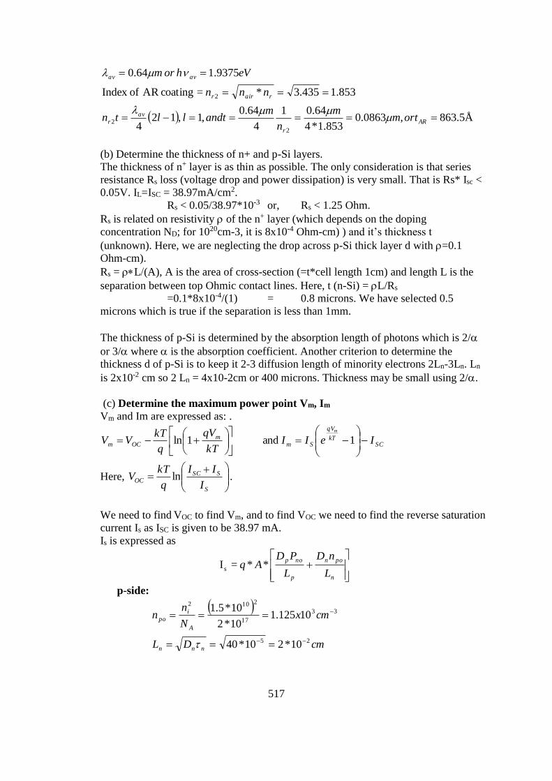
517
Å5.863,0863.0853.1*4
64.01
4
64.0,1 ,12
4
853.1435.3* =coating AR ofIndex
9375.1 64.0
2
2
2
AR
r
avr
rairr
avav
ortmm
n
mandtlltn
nnn
eVhorm
(b) Determine the thickness of n+ and p-Si layers.
The thickness of n+ layer is as thin as possible. The only consideration is that series
resistance Rs loss (voltage drop and power dissipation) is very small. That is Rs* Isc <
0.05V. IL=ISC = 38.97mA/cm2.
Rs < 0.05/38.97*10-3 or, Rs < 1.25 Ohm.
Rs is related on resistivity of the n+ layer (which depends on the doping
concentration ND; for 1020cm-3, it is 8x10⁻⁴ Ohm-cm) ) and it’s thickness t
(unknown). Here, we are neglecting the drop across p-Si thick layer d with =0.1
Ohm-cm).
Rs = L(A), A is the area of cross-section (=t*cell length 1cm) and length L is the
separation between top Ohmic contact lines. Here, t (n-Si) =L/Rs
=0.1*8x10-4/(1) = 0.8 microns. We have selected 0.5
microns which is true if the separation is less than 1mm.
The thickness of p-Si is determined by the absorption length of photons which is 2/
or 3/ where is the absorption coefficient. Another criterion to determine the
thickness d of p-Si is to keep it 2-3 diffusion length of minority electrons 2Ln-3Ln. Ln
is 2x10⁻² cm so 2 Ln = 4x10⁻²cm or 400 microns. Thickness may be small using 2/.
(c) Determine the maximum power point Vm, Im
Vm and Im are expressed as: .
SCkT
qV
Sm
m
OCm IeIIkT
qV
q
kTVV
m
1 and 1ln
Here,
S
SSCOC
I
II
q
kTV ln .
We need to find VOC to find Vm, and to find VOC we need to find the reverse saturation
current Is as ISC is given to be 38.97 mA.
Is is expressed as
n
pon
p
nop
L
nD
L
PDAq ** =Is
p-side:
cmDL
cmxN
nn
nnn
A
i
po
25
33
17
2102
10*210*40
10125.110*2
10*5.1

518
n+-side: (window region)
3
20
2102
25.210
10*5.1 cmN
np
D
ino
𝐿𝑝 = √𝐷𝑝𝜏𝑝 = √2 ∗ 10−6 ∗ 12.5 = 5 ∗ 10−3𝑐𝑚
𝐼𝑠 = 𝑞𝐴 [𝐷𝑛𝑛𝑝𝑜
𝐿𝑛+
𝐷𝑝𝑃𝑛𝑜
𝐿𝑝]
= 1.6 ∗ 10−19 ∗ 1 ∗ [40 ∗ 1.125 ∗ 103
2 ∗ 10−2+
12.5 ∗ 2.25
5 ∗ 10−3]
= 1.6 ∗ 10−19 ∗ 1 ∗ [40 ∗ 1.125 ∗ 103
2 ∗ 10−2+ 2.5 ∗ 2.5 ∗ 103]
= 0.361 ∗ 10−12A
S
SSCOC
I
II
q
kTV ln
=0.0259 ln[(38.97x10⁻³ + 0.361x10⁻¹²)/ 0.361x10⁻¹²]
VOC = 0.6579Volt
SCkT
qV
Smm
OCm IeIIkT
qV
q
kTVV
m
1 and 1ln
Substitute VOC and kT/q = 0.0259V in 1ln
kT
qV
q
kTVV m
OCm
Vm =
0259.01ln0259.06579.0 mV
. Since Vm is on both sides, we need to
write a short program or do trial and error substitution. We know Vm is less than
VOC, so we guess it to be 0.5V. for this guess we tabulate Left Hand Side (LHS)
and Right Hand Side (RHS) until the value of Vm makes both sides equal.
LHS RHS
0.5V(first guess) 0.5799
0.57 0.5766
0.576 0.5764
0.5765V 0.5764
So Vm = 0.5765V and Im is obtained by substituting Vm in the current equation.
Im = 0.36X10⁻¹²[exp(0.5765/0.0259) -1] -38.97X10-3
=1.675x10⁻³ -38.97x10-3 = -37.29 mA

519
Two curves related to solar spectral irradiance
(d) Compute dominant losses
(i) Reflection has been computed before.
(ii) We now compute the long wavelength photons that are not absorbed. These are
photons below the energy gap Eg = 1.1eV for Si. These are shown in the above Figure, in
area of region 1, 2 & 3, and a triangle F’/1.1 (D) /1.16 (D’) micron point on x-axis.
The solar power in these regions is:
Region #1 68.4 W/m2
Region #2 72.69 W/m2
Region #3 35.77 W/m2
These values have been calculated in solar design before.
Region #F’DD’ power is 16.5 W/m2 as shown below.
2'' /W5.1606.0*550*2
11.116.1*550*
2
1**
2
1mDDDFArea
Total long wavelength photon loss is 193.36 W/m2 or 19.36 mW/cm2.
The % of long wavelength light loss at AM1 in Si = %20925
36.193
(iii) We next calculate the Excess Energy Loss for photons above Eg or 1.1eV which have
more energy than needed to create an electron-hole pair.

520
Solar spectral irradiance for AM1
Excess photon energy not utilized in electron hole pair generation Si g,E-h =
Let AM1 plot above eV 1.1 hor m1.1 is divided in several regions. The exact way
is to find the area under the curve numerically. Regions are: Triangle 𝛼𝛽𝐽, Trapezoid
𝐽𝛽𝛾𝛿, Trapezoid marked as #4. These are calculated next.
Excess photon energy lost in spectral region represented by triangle 𝛼𝛽𝐽
eV11.21.121.3energyphoton Excess
12.32
43.24h
eV43.20.51
1.24at energy Photon
eV40.31
1.24at energy Photon J
eV
J
ave
Area if the 2/155
2
31.051.0*1550
2* mW
JJJ
Excess energy not used2/10111.2*
21.3
155mW

521
eVh
eVJatheVJathj
953.12
43.2476.1
43.251.0
24.1 ,43.2
51.0
24.1 Trapezoid
ave
2/5.4122/9501550*51.084.051.084.0*950 RectangleTrapezoid mWJ
Excess energy lost 2/05.178843.0*953.1/5.412 mW
Trapezoid #4, Rectangle #5 & Rectangle #6 can be combined by a rectangle
2/1301.184.0*500 mW
eVh ave 3.12
127.1476.1
2
1.1
24.1
84.0
24.1
Excess energy = eVEh gave 19.01.13.1
Excess energy not used =2/1919.0*
3.1
130mW
eV
Total excess energy loss = 101 + 178.05 + 19 = 298.05 W/m2.
(iv) Voltage factor is defined as the ratio of VOC and Eg/q.
Voltage factor =𝑉𝑜𝑐
𝐸𝑔/𝑞=0.6579/1.1 = 0.598.
The loss is 433.59 x 0.598 = 259.28W/m2, and the % loss is 259.28/925 = 28.03%. This
leaves available power of 174.31 W/m2.
(v) Fill Factor (FF) is defined as (VmIm)/(VOC ISC).
FF = [0.5765*37.29mA]/[0.6579*38.97mA] = 0.834 ~ 0.84.
The power loss due to FF is 0.84*174.31=27.89 W/m2. The % loss is 27.89/925 = 0.03%.
(vi) Collection efficiency of photo-generated electrons and holes. In crystalline Si this
loss may be 10%. However, it is significant in poly-crystalline Si substrates, where it is
~20%. A 10% loss reduces the available power to (146.42 – 14.64) 131.78 W/m2.
(vii) Series resistance loss: Series resistance loss Rs and other losses (see Fig. 19b).
100%
0%
18.9%
925 W/m2
731.64 W/m2
433.59 W/m2
46.93%
79.1%
146.42 W/m2
32.2% Loss
Fill Factor=0.84, Loss=27,89W/m2
Excess Energy (hѴave-Eg) loss, 298.05
193.36W/m2
Power
20.9% Loss Long Wavelength Loss
% Efficiency
Voltage Factor28.03%
259.28 W/m2 Loss 174.31 W/m
2
18.87%
Losses in Si solar cell.

522
2) Question 2
a) Power converted by the top cell
Incident power =ΔαßJ + Trapezoid ßγ'δ'J = ΔαßJ + Trapezoid ßγ'δ'J +γγ'δ'δ
Form Q.1 of this solution the area of various spectral regions are:
1- ΔαßJ =155 W/m²
2- Trapezoid ßγ'δ'J =412.5 W/m²
3- γγ'δ'δ =1010*(0.826-0.8) ; where δ'=0.826 , δ=0.8
=26.26 W/m²
Total power incident =593.76 W/m²
Assuming AR coating at top cell a-Si. The absorption coefficient αav ≈ 2*104 cm-1
Power transmitted = * 10*2*10*.015)-(0.5 4-4
e 593.76
= 593.76 e-0.615*2
= 593.76 e-1.230
= 173.53 W/m²
Power absorbed =593.76 - 173.53 = 420.22 W/m²
Power available to bottom cell = 173.53 W/m²
b) Top Cell Calculations: Find Voc, Vmp, Imp for top cell. In reality, this needs to be
calculated from power absorbed. Isc=7 mA is given.
)ln(s
sSC
I
II
q
kTVoc
Is for an amorphous a-Si cell can be calculated using ni value for a-Si. The ni is
proportional to exp(-Eg/kT). Although the effective masses are different, we get a ball
park value using the following.
p
nop
n
pon
s
aSiiaSiiaSii
L
pDAq
L
nDAqI
cmnenecSinin
******
10*64.6,*10*5.1|,*)(|
Dominates
36)
0259.0*2
4.0(
10)
0259.0*2
1.15.1(
Dn=0.8 cm2/s , τn=10-5 s ;Ln=(Dn* τn)1/2 = (8*10-6) 1/2=2.82*10-3 cm
AmpI
cmn
s
po
2020
3-
419
34
17
26
10*99.12.82
10*20.2*8.0*6.1
10*2.82
10*20.2*8.0*1*10*6.1
10*20.210*2
)10*64.6(
VVoc 04.1)10*99.1
10*7ln(*0259.0
20
3
, as Isc>>Is
And )0259.0
1ln(*0259.004.1)*
1ln( mmm
V
kT
Vq
q
kTVocV
1- Assume Vm=0.9V LHS=0.947
2- Assume Vm=0.95V LHS=0.946
3- Assume Vm=0.945V LHS=0.946
Vm=0.946V

523
AmpI
IIsI
m
SCm
33152030.0259
0.946
20
kT
qV
10*85.610*710*28.7*10*99.110*7)1e(*10*99.1
)1e(m
Im(top)=6.85*10-3 Amp
Bottom cell calculations:
Same Isc in the bottom cell is given, we can calculate Voc.
In a practice, Isc may not be same as the top cell. We need to calculated it from power
incident from the top cell and power absorbed.
)ln(,
,,
,
bs
bsbSC
bOCI
II
q
kTV
From Q.1 of this set for crystalline Si cell, Is=0.24*10-12A~Is,b.
VVOC 624.0)10*0.24
10*7ln(0259.0)
10*0.24
10*0.2410*7ln(0259.0
12-
3
12-
-123
Now we calculate maximum power point Vmb Imb for bottom cell.
)0259.0
1ln(*0259.0624.0)*
1ln(,
mbmbBOCmb
V
kT
Vq
q
kTVV
Vmb=0.543V as shown in the table.
AI
III
mb
bSCbsmb
33330.0259
0.543
20
,kT
qV
,
10*69.610*710*305.010*7)1e(*10*99.1
)1e(mp
Imb(bottom cell)=6.69*10-3 A.
c) Tandem cell will be have lower of two current
I Tandem m = 6.69*10-3 A
V Tandem = Vm-top + Vm-bottom - 0.03
Vmp(total) =0.946 +0.543 -0.03=1.459 V
Total Power
= (Vmp-top+ Vmp-bottom -0.03) Imp-Top ,or = (Vmp-top+ Vmp-bottom -0.03) Imp-Bottom
=1.459*6.85*10-3
=9.994 mW
1- Assume Vm=0.6V LHS=0.541
2- Assume Vm=0.55V LHS=0.543
3- Assume Vm=0.544V LHS=0.543

524
6. 13 Derivation of V-I equation in an n-p solar cell
nr2=1.8
p-SinrSi=3.45nair=1
AR coating
t
F Photon
flux
X=0 X=t+d
Back contact
Front
contact
Distribution of electrons in the neutral p-region. In this treatment we assume the junction
width to be very small as compared with diffusion lengths and photon absorption lengths.
The continuity equation is expressed in terms of optical generation rate Gop, carrier
recombination rate R and the divergence term due to non-uniform current density.
RG
dx
xJd
qdt
dnop
n 1
, (78)
the generation rate depends on the magnitude of photon flux per unit area per second
incident on the n-Si face. The absorption coefficient (h) is a function of photon energy h.
The electron current density is due to diffusion and expressed as
dx
xndDqxJ nn
(79)
n
x
n
nFe
dx
xndD
dt
dn
2
2
(80)
Under steady state dn/dt =0,
n
x
n
xnFe
dx
xndD
)(0
2
2
22
2 )(
n
x
L
xnFe
dx
xnd
(81)
The solution is
1sinhcosh)(
22
2
nn
x
n
nn LD
eLF
L
txD
L
txCxn
(82)
The solution depends on boundary conditions. They are
BC #1
1kT
qV
po entxnxn

525
BC#2 0 dtxn
Substituting BC#1
tkT
qV
po TeDCen
0*1*1 , here
122
2
nn
n
LD
LFT
1
11
22
2
kT
qV
po
t
nn
nkT
qV
po
t eneLD
LFenTeC
(83)
Using BC#2
dt
nn
TeL
dD
L
dC
sinhcosh0
Substituting C from Eq. (83)
)(sinhcosh10 dt
nn
kT
qV
po
t TeL
dD
L
denTe
n
kT
qV
po
n
dt
n
L
den
L
deTe
L
dD cosh1cosh
sinh
1 (84)
Substituting C and D in n(x)
x
nn
kT
qV
po
n
dt
n
n
kT
qV
po
t
TeL
tx
L
den
L
deTe
L
d
L
txenTexn
sinhcosh1coshcosech
cosh1
(85)
The current density is x
xqDxJ n
nn
(86)
x
n
nn
kT
qV
po
n
dt
n
n
kT
qV
po
t
n
n
n
TeLL
tx
L
den
L
deTe
L
d
L
txenTe
L
DqxJ
coshcosh1coshcosech
sinh1
(87)
The current density at the junction boundary x = t
t
n
n
kT
qV
po
n
dt
nn
n
n TeLL
den
L
deTe
L
d
L
qDtxJ cosh1coshcosech
n
kT
qV
po
nn
d
n
t
n
n
nL
den
L
d
L
deLTe
L
qDtxJ coth1cothcosech (88)
Hole concentration in the window n-region: t +d > x > t, the continuity equation is

526
RG
dx
xJd
qdt
dpop
p
1 (89)
Under steady state, there is no time variation
p
xp xpeN
dx
xJd
q
1
0
N=Number of photon incidence per unit area per second= F
Under Steady State
p
xp xpeNq
dx
xJd
(90)
dx
pdDqxJ pp
, we neglect the drift term and also use F in place of N (91)
p
x
p
xpeFq
dx
pdqD
2
2
22
2
pp
x
L
xp
D
eF
dx
pd
(92)
x
pp
p
pp
eLD
LF
L
xB
L
xAxp
1sinhcosh)(
22
2
(93)
This can be written as
x
pp
eRL
xB
L
xAp
sinhcosh (94)
Where 122
2
pp
p
LD
FLR
(95)
The boundary conditions are
1
1# kT
qv
noeptxptxBC (96)
00,02# pqSJxBCand p (97)
Here, S is the surface recombination velocity at the x=0 interface.
Substituting the boundary condition BC#1 in p(x) expression at x= t
t
pp
kT
qV
no eRL
tB
L
tAep
sinhcosh1
tkT
qV
no
pp
eRepL
tB
L
tA
1sinhcosh (98)
Substituting the boundary condition BC#1 at x=0,
00*1* pJRBASq
0pJRqSASq (99)
We next find the Jp(0) expression.

527
x
p
ppp
p
x
pppp
p
pp
eRLL
xB
L
xA
L
qD
eRL
x
L
B
L
x
L
AqD
x
xpqDxJ
coshsin
coshsinh
)(
(100)
RqDBL
qDRLBA
L
qDJ p
p
p
p
p
p
p 0*)0( (101)
Substitute Eq. 101 Jp(0) in BC#1 Eq.99
Multiply by ‘-1’ and divide by qS
qS
RqD
qSL
BqD
qS
RSq
qS
ASq p
p
p
This gives
,S
RD
SL
BDRA
p
p
p
S
DR
SL
DBA
p
p
p 1 (102)
Substitute for A in Eq.98 to get an expression for B
Eq.3Re1sinhcosh tkT
qV
no
pp
p
p
peP
L
tB
L
t
S
DSR
LS
DB
Collect ‘B’ terms
tkT
qV
no
p
p
ppp
pep
L
t
S
DSR
L
t
L
t
LS
DB
Re1coshsinhcosh
ppp
p
tkT
qV
no
p
p
L
t
L
t
LS
D
epL
t
S
DSR
B
sinhcosh
Re1cosh
(103)
RqDBL
qDRSqASq p
p
p

528
Substitute B in Eq. 102 to get A
S
DR
L
t
L
t
LS
D
epL
t
S
DSR
LS
DA
p
ppp
p
tkT
qV
no
p
p
p
p
S
sinhcosh
Re1cosh
(104)
Reproduce equation 100
x
p
ppp
p
p LL
BL
AL
DqxJ Re
xcosh
xsinh
(100)
Jp at junction boundary x = t
t
p
ppp
p
p LL
BL
AL
DqtJ Re
tcosh
tsinh (105)
Substitute A from 104 & B from 103
Eq.7
sinhcosh
Re1cosh
*cosh
*sinhcosh
Re1cosh
*sinh
t
p
p
p
ppp
p
tkT
qV
no
p
p
pp
p
p
ppp
p
tkT
qV
no
p
p
p
p
pp
p
p
eRLL
Dq
L
t
L
t
LS
D
epL
t
S
DSR
L
t
L
Dq
S
DSR
L
t
L
t
LS
D
epL
t
S
DSR
LS
D
L
t
L
DqtJ
Cancelling Dp/SLp term from numerator and denominator in the first term,
t
pp
pp
p
pp
p
tkT
qV
no
p
p
pp
p
pp
p
p
tkT
qV
no
p
p
pp
p
p
eRLDq
L
t
D
LS
L
t
LS
D
epL
t
S
DR
L
t
L
Dq
L
t
D
LS
L
t
epL
t
S
DR
L
t
L
DqtJ
sinhcosh
Re1cosh1
*cosh
sinhcosh
Re1cosh1
*sinh
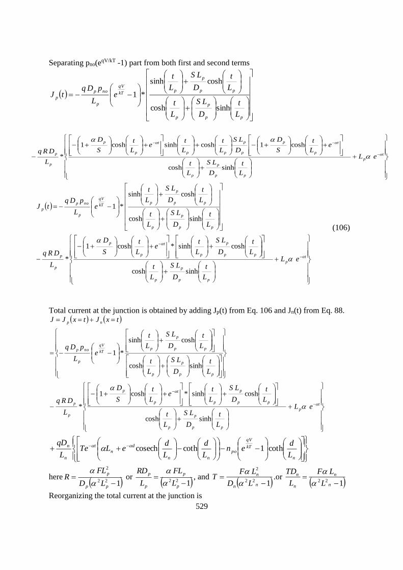
529
Separating pno(e
qV/kT -1) part from both first and second terms
pp
p
p
pp
p
pkT
qV
p
nop
p
L
t
D
LS
L
t
L
t
D
LS
L
t
eL
pDqtJ
sinhcosh
coshsinh
*1
t
p
pp
p
p
t
p
p
p
p
pp
t
p
p
p
peL
L
t
D
LS
L
t
eL
t
S
D
D
LS
L
t
L
te
L
t
S
D
L
DRq
sinhcosh
cosh1coshsinhcosh1
*
t
p
pp
p
p
pp
p
p
t
p
p
p
p
pp
p
p
pp
p
pkT
qV
p
nop
p
eL
L
t
D
LS
L
t
L
t
D
LS
L
te
L
t
S
D
L
DRq
L
t
D
LS
L
t
L
t
D
LS
L
t
eL
pDqtJ
sinhcosh
coshsinh*cosh1
*
sinhcosh
coshsinh
*1
(106)
Total current at the junction is obtained by adding Jp(t) from Eq. 106 and Jn(t) from Eq. 88.
t
p
pp
p
p
pp
p
p
t
p
p
p
p
pp
p
p
pp
p
pkT
qV
p
nop
np
eL
L
t
D
LS
L
t
L
t
D
LS
L
te
L
t
S
D
L
DRq
L
t
D
LS
L
t
L
t
D
LS
L
t
eL
pDq
txJtxJJ
sinhcosh
coshsinh*cosh1
*
sinhcosh
coshsinh
*1
n
kT
qV
po
nn
d
n
t
n
n
L
den
L
d
L
deLTe
L
qDcoth1cothcosech
here 122
2
pp
p
LD
FLR
or
122
p
p
p
p
L
FL
L
RD
, and
122
2
nn
n
LD
LFT
.or
122
n
n
n
n
L
LF
L
TD
Reorganizing the total current at the junction is

530
t
p
pp
p
p
pp
p
p
t
p
p
p
p
nn
pon
pp
p
p
pp
p
p
p
nopkT
qV
eL
L
t
D
LS
L
t
L
t
D
LS
L
te
L
t
S
D
L
LFq
L
d
L
nDq
L
t
D
LS
L
t
L
t
D
LS
L
t
L
pDqeJ
sinhcosh
coshsinh*cosh1
*1
coth
sinhcosh
coshsinh
**1
22
n
t
n
dtt
nn
n
L
de
L
deeL
L
LFq cothcosech
1
)(
22
(107)
The current can be written as
SC
kT
qV
S JeJJ 1 (108)
Where reverse saturation current density Js of a dark diode is
nn
pon
pp
p
p
pp
p
p
p
nop
SL
d
L
nDq
L
t
D
LS
L
t
L
t
D
LS
L
t
L
pDqJ coth
sinhcosh
coshsinh
* (109)
And photo-generated short circuit current density Jsc is
t
p
pp
p
p
pp
p
p
t
p
p
p
p
SC eL
L
t
D
LS
L
t
L
t
D
LS
L
te
L
t
S
D
L
LFqJ
sinhcosh
coshsinh*cosh1
*122
n
t
n
dtt
nn
n
L
de
L
deeL
L
LFq cothcosech
1
)(
22
(110)
The numerator in Jsc term
pp
p
p
t
p
p
L
t
D
LS
L
te
L
t
S
Dcoshsinh*cosh1
, simplifies to
=
pp
p
p
tp
pp
p
pL
t
D
LS
L
te
S
D
L
t
D
LSL coshsinh1
=
pp
p
p
t
p
p
pL
t
D
LS
L
te
D
LSL coshsinh , as
S
D
L
t p
p
1 is negligible.
Solar spectrum is covered if we sum q
eVh
Egh d
dp
hF
40 1q is the quantum efficiency.

531
6.13 Solar cell summary equations
Air mass m is definedzenithat is sun the whenlength path
tmeasuremen of timeat thesunlight theof length path opticalm .
Air mass m=2 or 1.5 is taken as a typical average for the day. At m=2, we have 74mW/cm2
which produces ISC = 27mA for a cell sample of 1cm2.
IL
ID
RS h
RS
I
RL
V-I Equation : Equivalent Circuit Approach
Generally, the behavior of a solar cell is modeled by the following equations. IL or ISC is the
current under short circuit condition generated by absorption of photons.
)I (orI-1)-e(I=I scLkT
qV
s (27)
Open circuit voltage is obtained by putting I=0 in Eq. 27 an rearranging terms.
I
I+I
q
kT=V
s
sLoc ln (36)
Maximum power point (Vm, Im) is obtained using I
V-=
I
V
, or
V
I-=
V
I
(40a, 40b) and Eq.
(27)
kT
Vq+1
q
kT-V=V
mocm ln (48)
Equation (48) can be solved numerically. Substituting Vm in Equation (27) results in an
expression for Im.
I-1]-e[I=I LkT
Vq
sm
m
(49)
Fill Factor: FF: The fill factor is related to the shape of the V-I plot.
rectangle outer of Area
rectangle inner of Area=
IV
P=
IV
IV=FF
Loc
m
Loc
mm
(50)
Photon energy required to generate an electron hole pair (EHP) = Eg= 1.1 eV in Si.
Excess energy per photon of energy = h (eV) – Eg = 1.5 1.1eV = 0.4eV (if hv = 1.5eV).
Excess energy not used to create electron hole pairs: If the power absorbed is Pabs1 and

532
average photon energy is hv, the excess energy
= Number of photon absorbed per sec x (hv – Eg).
Number of Photons absorbed / sec = sec/10*58.110*6.1*5.1
10*8.3 16
19
3
1 photonsh
Pabs
LOSSES: 1. Surface reflection:
Calculate reflectivity R = Reflectivity of Si = R = 3.01435.3
1435.322
airr
airr
nn
nn
Remedy: Design an antireflection coating using nr2 film
nr2=1.8
Si
nr=3.45nair=1
AR coating
t
Fig. 20 Antireflection coating. Fig. 32. Solar spectral irradiance for AM1.
)12(4 2
ln
tr
, photons of 1.5 eV, m
eVh
8266.0
5.1
24.124.1 )12(
8.1*4
10*8266.0 4
lt
,l =1,2
2. Long wavelength photons are not absorbed when hv < Eg. (as is very small.
3. Excess photon energy loss: Calculation (see design set page 414): Photon energy above
Eg is not used to generated electron-hole pairs (EHPs). This does not contribute to short
circuit current ISC or IL. Compute these losses: AM1 plot above h > 1.1eV
Regions are Triangle J, Trapezoid J, Trapezoid marked as #4, small rectangular regions
#5 & #6.
(triangle) J => Photon energy at = eV431.0
24.1
Photon energy at J = eV43.251.0
24.1 Average photon energy eVh ave 21.3
2
43.24
Excess photon energy not used in generating EHP= 3.21 – 1.1 = 2.11eV.
Area of the J = 2/155
2
31.051.0*1550
2* mW
JJ
Excess energy not used in triangle J is = 2/10111.2*
21.3
155mW

533
6.14 References 1. J. M. Olson and D. J. Friedman, High Efficiency iii-V Solar Cells, Compound
Semiconductor, Vol. 2, pp. 27-29, November /December 1996.
2. R. Metzger, Manufacturing III-V Solar Cells for Space Applications, Compound
Semiconductor, Vol. 2, pp. 25-26, November /December 1996.
3. M. Meyer and R. Metzger, Flying High: The Commercial Satellite Industry Converts to
Compound Semiconductor Solar Cells, Compound Semiconductor, Vol. 2, pp. 22-24,
November /December 1996.
4. K.A. Bertness, S. Kurtz, D.J. Friedman, A.E. Kibbler, C. Kramer, and J.M. Olson, 29.5%-
efficient GaInP/GaAs tandem solar cells, Appl. Phys. Lett., 65, pp. 989-991, August 1994.
5. N. Dharmarasu, M. Yamaguchi, and A. Khan, T. Yamada, T. Tanabe, S. Takagishi, T.
Takamoto, T. Ohshima, H. Itoh, M. Imaizumi and S. Matsuda, Appl. Phys. Lett., 79, pp. 2399-
2401, October 2001.
6. S. Licht, B. Wang, T. Soga, and M. Umeno, Light invariant, efficient, multiple band gap
AlGaAs/Si/metal hydride solar cell, Appl. Phys. Lett., 74, pp. 4055-4057, June 1999.
7. N. J. Ekins-Daukes, K.W. J. Barnham, J. P. Connolly, J.S. Roberts, J.C. Clark, and G. Hill,
Strain-balanced GaAsP/InGaAs quantum well solar cells, Appl. Phys. Lett., 75, pp. 4195-4197,
December 1999.
8. D. W. Parent, A. Rodriguez, J. E. Ayers, and F. C. Jain, Photoassisted MOVPE Grown (n)
ZnSe/(p+)GaAS heterojunction solar cells, Solid-State Electronics, 47, pp. 595-599, 2003.
9. F. C. Jain, Observation of an active photoinductive component in high intensity solar cells.
J. App. Phys. 51, p. 2685, 2000.
10. S. M. Sze, Physics of Semiconductors, Wiley-Interscience, New York, 1981.
11. A.C. Miles, Semiconductor Devices and Integrated Circuits, Van Nostrand, Reinhold, p.736
1980.
12. R.A Metzger, Manufacturing III-V Solar cells for space Application, Page 25,
Compound Semiconductor November / December 1996.
13. Mary Archer and Bob Hill, Eds., Clean Energy from Photovoltaics (1st Edition), Series on
Photoconversion of Solar Energy – Vol. 1, (Imperial College Press, London, 2001).[covers
Amorphous Silicon Solar Cells by C. Wronski and D. Carlson, Cadmium Telluride Solar
Cells –by D. Bonnet, Cu(In,Ga)Se- Solar Cells by U. Rau and H. Schock.
14. A. Luque and S. Hegedus, Eds. Handbook of Photovoltaics Science and Engineering
(Wiley, West Sussex, 2003), Cadmium Telluride Solar Cells by B.E. McCandless and J. R.
Sites.
15. J. Poortmans and V. Arkhipov, Eds., Thin Film Solar Cells: Fabrication, Characterization,
and Applications (Wiley, West Sussex, 2006). [covers Chalcopyrite Based Solar Cells. R.
Klenk and M. C. Lux-Stiner, and Cadmium Telluride Solar Cells byMarc Burgelman.]
16, Lewis Fraas and Larry Partain, Eds., Solar Cells and Their Applications, 2nd Edition,
(Wiley, New Jersey, 2010). See Thin-Film Solar Cells and Modules by Robert Birkmier.
17.W. van Sark, Ed. Comprehensive Renewable Energy, Volume 1: Photovoltaic Solar Energy
(Elsevier, 2012).[covers Thin-Film Silicon PV Technology by R.E.I. Schorpp, Chalcopyrite
Thin Film Materials and Solar Cells byT. Unold and C.A. Kaufmann, and Cadmium
Telluride Photovoltaic Thin Film Solar Cells by T.A. Gessert.
18. A.J. Nozik, M.C. Beard, and G. Conibeer, Eds. Advanced Concepts in Photovoltaics,
Royal Society of Chemistry (RSC) Publishing, London, 2014. See “Thin-Film CdTe
Photovoltaic Solar Cell Devices,” by T.A. Gessert, B. McCandless, and C. Ferekides.
19.Mary Archer and Martin Greene, Eds. Clean Energy from Photovoltaics, 2nd Edition, Series
on Photoconversion of Solar Energy – Vol. 1, World Series Publishing, London, 2014). See

534
Polycrystalline Cadmium Telluride Photovoltaic Devices by T.A. Gessert and D. Bonnet.
20. J. Perrenoud, S. Buecheler, A.N. Tiwari, “Flexible CdTe Solar Cells with High
Photovoltaic Conversion Efficiency”, 2009 IEEE Conference, p.695-699, 2009.
21. A. M. Green , K. Emery , Y. Hishikawa , and W. Warta . Prog. Photovoltaics 17 , 85 – 94 ( 2009).