lab 6: memories: external spi flash and ddr2 · lab 6: memories: external spi flash and ddr2 ......
TRANSCRIPT
1
Lab 6: Memories: External SPI Flash and DDR2 EE-459/500 HDL Based Digital Design with Programmable Logic
Electrical Engineering Department, University at Buffalo
Last update: Cristinel Ababei, 2012
1. Objective
The objective of this lab is to learn how to access memory chips from within your VHDL design. These
memory chips are external to the FPGA, located on the Atlys board. The board has a 16Mbyte x4 SPI Flash
for configuration and data storage and a 128Mbyte DDR2 with 16-bit wide data.
2. Description
The Atlys board uses a 128Mbit Numonyx N25Q12 Serial Flash memory device (16,777,216 bytes - 8 bits
each) for non-volatile storage of FPGA configuration files. The SPI Flash can be programmed with a .bit,
.bin., or .mcs file using the Adept software. Adept Flash programming application allows also allows user
data files to be transferred to/from the Flash at user specified addresses. The Read/Write tools of Adept
allow data to be exchanged between files on the host PC and specified address ranges in Flash.
As general-purpose flash, the SPI serial flash can also be used for any other non-volatile storage that you
might require. One example could be to store MicroBlaze processor application code for bootloading.
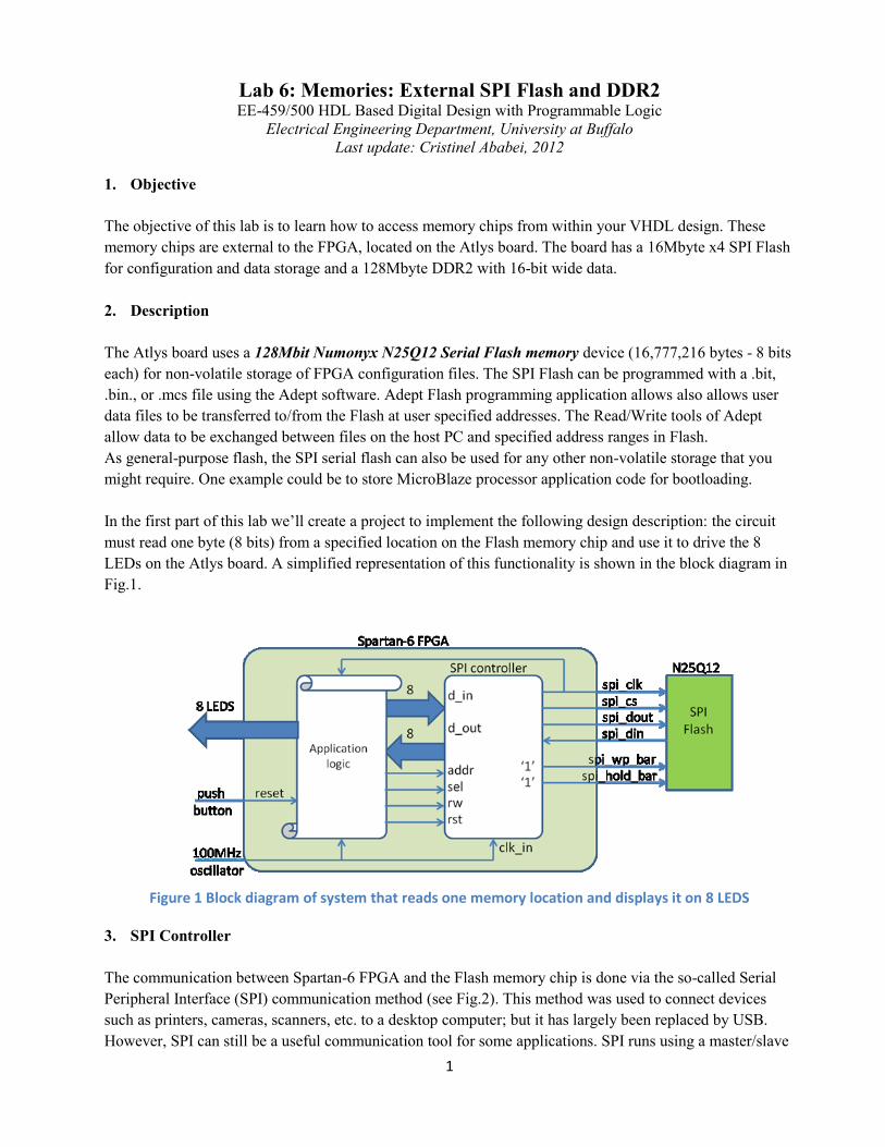
In the first part of this lab we’ll create a project to implement the following design description: the circuit
must read one byte (8 bits) from a specified location on the Flash memory chip and use it to drive the 8
LEDs on the Atlys board. A simplified representation of this functionality is shown in the block diagram in
Fig.1.
3. SPI Controller
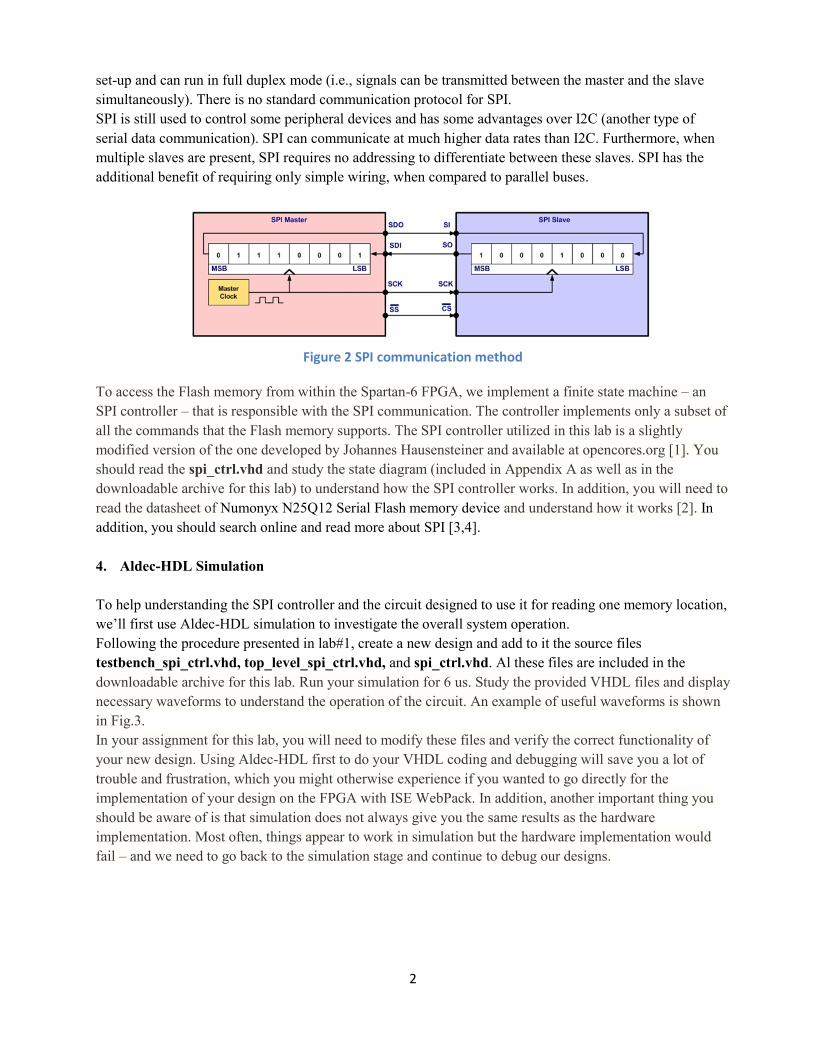
The communication between Spartan-6 FPGA and the Flash memory chip is done via the so-called Serial
Peripheral Interface (SPI) communication method (see Fig.2). This method was used to connect devices
such as printers, cameras, scanners, etc. to a desktop computer; but it has largely been replaced by USB.
However, SPI can still be a useful communication tool for some applications. SPI runs using a master/slave
Figure 1 Block diagram of system that reads one memory location and displays it on 8 LEDS
2
set-up and can run in full duplex mode (i.e., signals can be transmitted between the master and the slave
simultaneously). There is no standard communication protocol for SPI.
SPI is still used to control some peripheral devices and has some advantages over I2C (another type of
serial data communication). SPI can communicate at much higher data rates than I2C. Furthermore, when
multiple slaves are present, SPI requires no addressing to differentiate between these slaves. SPI has the
additional benefit of requiring only simple wiring, when compared to parallel buses.
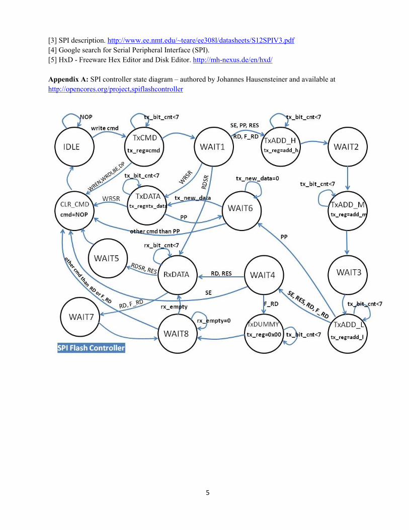
To access the Flash memory from within the Spartan-6 FPGA, we implement a finite state machine – an
SPI controller – that is responsible with the SPI communication. The controller implements only a subset of
all the commands that the Flash memory supports. The SPI controller utilized in this lab is a slightly
modified version of the one developed by Johannes Hausensteiner and available at opencores.org [1]. You
should read the spi_ctrl.vhd and study the state diagram (included in Appendix A as well as in the
downloadable archive for this lab) to understand how the SPI controller works. In addition, you will need to
read the datasheet of Numonyx N25Q12 Serial Flash memory device and understand how it works [2]. In
addition, you should search online and read more about SPI [3,4].
4. Aldec-HDL Simulation
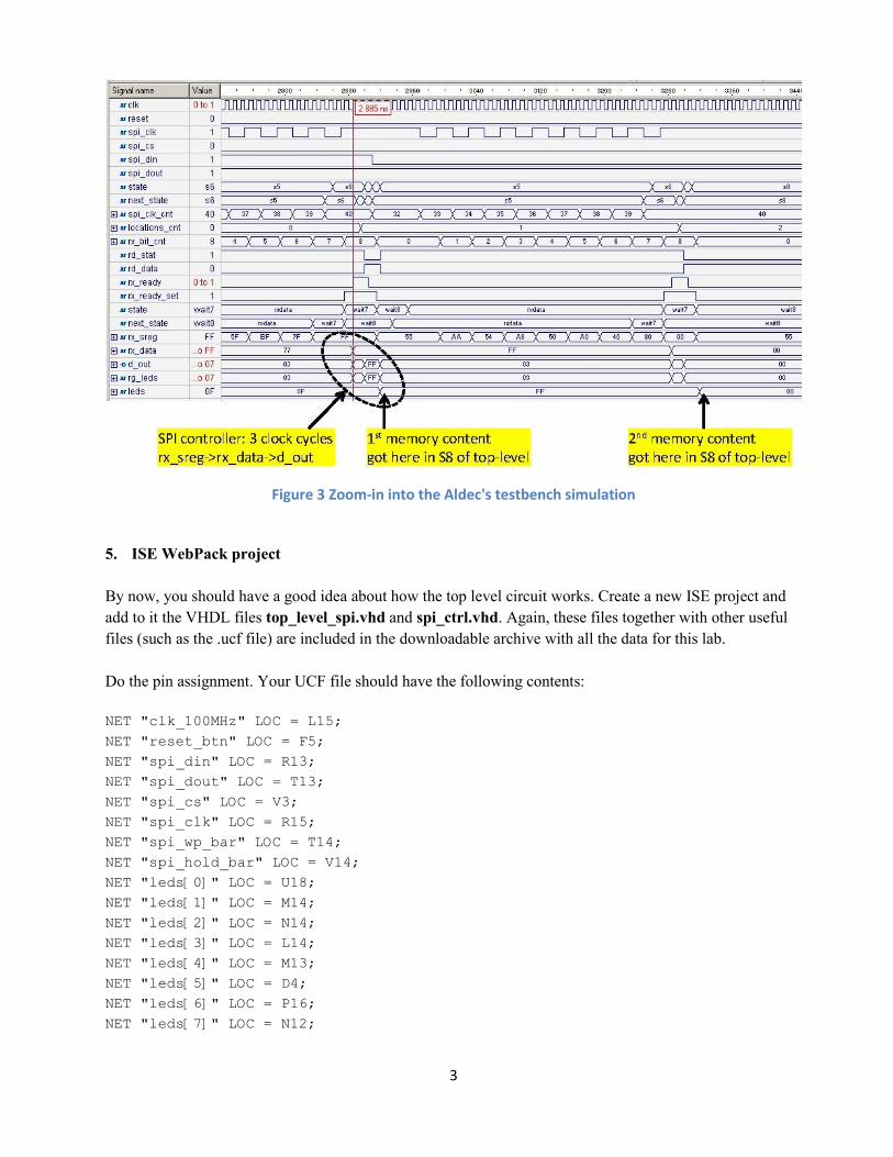
To help understanding the SPI controller and the circuit designed to use it for reading one memory location,
we’ll first use Aldec-HDL simulation to investigate the overall system operation.
Following the procedure presented in lab#1, create a new design and add to it the source files
testbench_spi_ctrl.vhd, top_level_spi_ctrl.vhd, and spi_ctrl.vhd. Al these files are included in the
downloadable archive for this lab. Run your simulation for 6 us. Study the provided VHDL files and display
necessary waveforms to understand the operation of the circuit. An example of useful waveforms is shown
in Fig.3.
In your assignment for this lab, you will need to modify these files and verify the correct functionality of
your new design. Using Aldec-HDL first to do your VHDL coding and debugging will save you a lot of
trouble and frustration, which you might otherwise experience if you wanted to go directly for the
implementation of your design on the FPGA with ISE WebPack. In addition, another important thing you
should be aware of is that simulation does not always give you the same results as the hardware
implementation. Most often, things appear to work in simulation but the hardware implementation would
fail – and we need to go back to the simulation stage and continue to debug our designs.
Figure 2 SPI communication method
3
5. ISE WebPack project
By now, you should have a good idea about how the top level circuit works. Create a new ISE project and
add to it the VHDL files top_level_spi.vhd and spi_ctrl.vhd. Again, these files together with other useful
files (such as the .ucf file) are included in the downloadable archive with all the data for this lab.
Do the pin assignment. Your UCF file should have the following contents:
NET "clk_100MHz" LOC = L15;
NET "reset_btn" LOC = F5;
NET "spi_din" LOC = R13;
NET "spi_dout" LOC = T13;
NET "spi_cs" LOC = V3;
NET "spi_clk" LOC = R15;
NET "spi_wp_bar" LOC = T14;
NET "spi_hold_bar" LOC = V14;
NET "leds[0]" LOC = U18;
NET "leds[1]" LOC = M14;
NET "leds[2]" LOC = N14;
NET "leds[3]" LOC = L14;
NET "leds[4]" LOC = M13;
NET "leds[5]" LOC = D4;
NET "leds[6]" LOC = P16;
NET "leds[7]" LOC = N12;
Figure 3 Zoom-in into the Aldec's testbench simulation
4
Run the “Implement Design” step inside ISE WebPack to perform placement and routing and observe the
messages that the tool prints in the Console window. These messages provide useful information about the
resource utilization on the FPGA as well as performance estimates.
Generate the programming .bit file and program the FPGA. Verify the operation of your design. Observe
and comment.
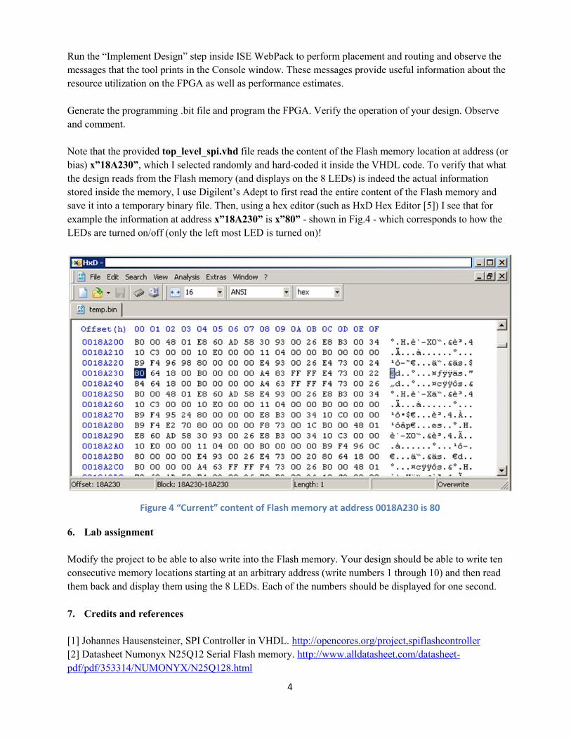
Note that the provided top_level_spi.vhd file reads the content of the Flash memory location at address (or
bias) x”18A230”, which I selected randomly and hard-coded it inside the VHDL code. To verify that what
the design reads from the Flash memory (and displays on the 8 LEDs) is indeed the actual information
stored inside the memory, I use Digilent’s Adept to first read the entire content of the Flash memory and
save it into a temporary binary file. Then, using a hex editor (such as HxD Hex Editor [5]) I see that for
example the information at address x”18A230” is x”80” - shown in Fig.4 - which corresponds to how the
LEDs are turned on/off (only the left most LED is turned on)!
6. Lab assignment
Modify the project to be able to also write into the Flash memory. Your design should be able to write ten
consecutive memory locations starting at an arbitrary address (write numbers 1 through 10) and then read
them back and display them using the 8 LEDs. Each of the numbers should be displayed for one second.
7. Credits and references
[1] Johannes Hausensteiner, SPI Controller in VHDL. http://opencores.org/project,spiflashcontroller
[2] Datasheet Numonyx N25Q12 Serial Flash memory. http://www.alldatasheet.com/datasheet-
pdf/pdf/353314/NUMONYX/N25Q128.html
Figure 4 “Current” content of Flash memory at address 0018A230 is 80
5
[3] SPI description. http://www.ee.nmt.edu/~teare/ee308l/datasheets/S12SPIV3.pdf
[4] Google search for Serial Peripheral Interface (SPI).
[5] HxD - Freeware Hex Editor and Disk Editor. http://mh-nexus.de/en/hxd/
Appendix A: SPI controller state diagram – authored by Johannes Hausensteiner and available at
http://opencores.org/project,spiflashcontroller