lab manual - welcome to channabasaveshwara … and lic lab_iv sem.pdflab manual ( 2016 – ‘17)...
TRANSCRIPT

QMP 7.1 D/F
Channabasaveshwara Institute of Technology (An ISO 9001:2008 Certified Institution)
NH 206 (B.H. Road), Gubbi, Tumkur – 572 216. Karnataka.
Department of Electrical & Electronics Engineering
LAB MANUAL
( 2016 – ‘17)
15EEL48
OP- AMP AND LINEAR ICS LABORATORY
IV Semester E&E Engineering
Name : _________________________________________________
U S N : _________________________________________________
Batch : _____________________ Section : _______________

Channabasaveshwara Institute of Technology (An ISO 9001:2008 Certified Institution)
NH 206 (B.H. Road), Gubbi, Tumkur – 572 216. Karnataka.
Department of Electrical & Electronics Engineering
OP- AMP AND LINEAR ICS LABORATORY Version 1.0
Feb 2017
Prepared by: Reviewed by:
Mrs.Prathibha T Mrs. Lokanathan M S
Mrs. Roopa S Assistant Professor
Assistant Professor
Approved by:
Prof. V C Kumar
Professor & Head,
Dept. of EEE

Channabasaveshwara Institute of Technology
(An ISO 9001:2008 Certified Institution)
NH 206 (B.H. Road), Gubbi, Tumkur – 572 216. Karnataka.
OUR VISION
To create centers of excellence in education and to serve the society by enhancing the quality of
life through value based professional leadership.
OUR MISSION
To provide high quality technical and professionally relevant education in a diverse learning
environment.
To provide the values that prepare students to lead their lives with personal integrity,
professional ethics and civic responsibility in a global society.
To prepare the next generation of skilled professionals to successfully compete in the diverse
global market.
To promote a campus environment that welcomes and honors women and men of all races,
creeds and cultures, values and intellectual curiosity, pursuit of knowledge and academic
integrity and freedom.
To offer a wide variety of off-campus education and training programmes to individuals and
groups.
To stimulate collaborative efforts with industry, universities, government and professional
societies.
To facilitate public understanding of technical issues and achieve excellence in the operations of
the institute.
QUALITY POLICY
Our organization delights customers (students, parents and society) by providing value added
quality education to meet the national and international requirements. We also provide necessary
steps to train the students for placement and continue to improve our methods of education to the
students through effective quality management system, quality policy and quality objectives.
Channabasaveshwara Institute of Technology
(An ISO 9001:2008 Certified Institution)
NH 206 (B.H. Road), Gubbi, Tumkur – 572 216. Karnataka.
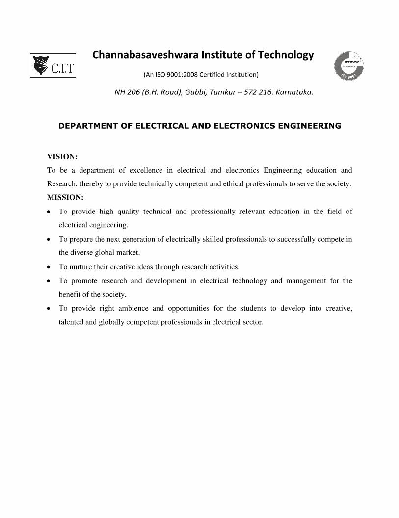
DEPARTMENT OF ELECTRICAL AND ELECTRONICS ENGINEERING
VISION:
To be a department of excellence in electrical and electronics Engineering education and
Research, thereby to provide technically competent and ethical professionals to serve the society.
MISSION:
To provide high quality technical and professionally relevant education in the field of
electrical engineering.
To prepare the next generation of electrically skilled professionals to successfully compete in
the diverse global market.
To nurture their creative ideas through research activities.
To promote research and development in electrical technology and management for the
benefit of the society.
To provide right ambience and opportunities for the students to develop into creative,
talented and globally competent professionals in electrical sector.

SYLLABUS
OP- AMP AND LINEAR ICS LABORATORY
Sub Code: 15EEL48 IA Marks: 20
Hrs/ Week: 03 Exam Hours: 03
Total Hrs. 42 Exam Marks: 80
1. Design and verify a precision full wave rectifier. Determine the performance
parameters.
2 . Design and realize to analyse the frequency response of an op – amp amplifier under
Inverting and non - inverting configuration for a given gain.
3. Design and verify the output waveform of an op – amp RC phase shift oscillator for a
desired frequency.
4. Design and realize Schmitt trigger circuit using an op – amp for desired upper trip
point (UTP) and lower trip point (LTP).
5. Verify the operation of an op – amp as (a) voltage comparator circuit and (b) zero
crossing detector.
6. Design and verify the operation of op – amp as an (a) adder (b) subtractor (c)
integrator and (d) differentiator.
7. Design and realize an op – amp based first order Butterworth (a) low pass (b) high
pass and (c) band pass filters for a given cut off frequency/frequencies to verify the
frequency response characteristic.
8. Design and realize an op – amp based function generator to generate sine, square and
triangular waves of desired frequency.
9. Design and realization of R – 2R ladder DAC.
10. Realization of Two bit Flash ADC.
11. Design and verify an IC 555 timer based pulse generator for the specified pulse.
12 . Designing of Fixed voltage power supply (voltage regulator) using IC regulators 78
series and 79 series.

‘Instructions to the Candidates’
1. Students should come with thorough preparation for the experiment to
be conducted.
2. Students will not be permitted to attend the laboratory unless they bring
the practical record fully completed in all respects pertaining to the
experiment conducted in the previous class.
3. Experiment should be started only after the staff-in-charge has checked
the circuit diagram.
4. All the calculations should be made in the observation book. Specimen
calculations for one set of readings have to be shown in the practical
record.
5. Wherever graphs are to be drawn, A-4 size graphs only should be used
and the same should be firmly attached to the practical record.
6. Practical record should be neatly maintained.
7. The students should obtain the signature of the staff-in-charge in the
observation/manual book after completing each experiment.
8. Theory regarding each experiment should be written in the practical
record before procedure in your own words.
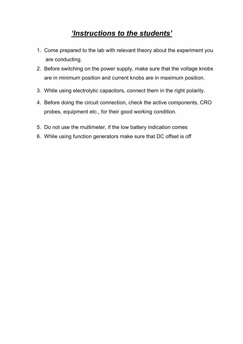
‘Instructions to the students’
1. Come prepared to the lab with relevant theory about the experiment you
are conducting.
2. Before switching on the power supply, make sure that the voltage knobs
are in minimum position and current knobs are in maximum position.
3. While using electrolytic capacitors, connect them in the right polarity.
4. Before doing the circuit connection, check the active components, CRO
probes, equipment etc., for their good working condition.
5. Do not use the multimeter, if the low battery indication comes
6. While using function generators make sure that DC offset is off
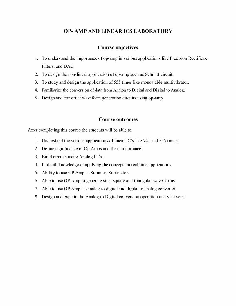
OP- AMP AND LINEAR ICS LABORATORY
Course objectives
1. To understand the importance of op-amp in various applications like Precision Rectifiers,
Filters, and DAC.
2. To design the non-linear application of op-amp such as Schmitt circuit.
3. To study and design the application of 555 timer like monostable multivibrator.
4. Familiarize the conversion of data from Analog to Digital and Digital to Analog.
5. Design and construct waveform generation circuits using op-amp.
Course outcomes
After completing this course the students will be able to,
1. Understand the various applications of linear IC’s like 741 and 555 timer.
2. Define significance of Op Amps and their importance.
3. Build circuits using Analog IC’s.
4. In-depth knowledge of applying the concepts in real time applications.
5. Ability to use OP Amp as Summer, Subtractor.
6. Able to use OP Amp to generate sine, square and triangular wave forms.
7. Able to use OP Amp as analog to digital and digital to analog converter.
8. Design and explain the Analog to Digital conversion operation and vice versa

Channabasaveshwara Institute of Technology (An ISO 9001:2008 Certified Institution)
NH 206 (B.H. Road), Gubbi, Tumkur – 572 216. Karnataka.
DEPARTMENT OF ELECTRICAL & ELECTRONICS ENGG.
CONTENTS
Exp.
No Title of the Experiment
Page
No
1 Design and verify a precision full wave rectifier. Determine the
performance parameters. 2
2
Design and realize to analyse the frequency response of an op – amp
amplifier under Inverting and non - inverting configuration for a given
gain. 6
3
Design and verify the output waveform of an op – amp RC phase shift
oscillator for a desired frequency. 10
4 Design and realize Schmitt trigger circuit using an op – amp for desired
upper trip point (UTP) and lower trip point (LTP). 14
5 Verify the operation of an op – amp as (a) voltage comparator circuit and
(b) zero crossing detector. 18
6 Design and verify the operation of op – amp as an (a) adder (b) subtractor
(c) integrator and (d) differentiator. 20
7 Design and realize an op – amp based first order Butterworth (a) low pass (b) high pass and (c) band pass filters for a given cut off frequency/frequencies to verify the frequency response characteristic.
26
8 Design and realize an op – amp based function generator to generate sine,
square and triangular waves of desired frequency. 34
9 Design and realization of R – 2R ladder DAC. 36
10 Realization of Two bit Flash ADC. 40
11 Design and verify an IC 555 timer based pulse generator for the specified
pulse. 42
12 Designing of Fixed voltage power supply (voltage regulator) using IC
regulators 78 series and 79 series. 46

References 49
Annexure
Viva Questions 50
Question Bank 52
Appendix 53
OP- AMP AND LINEAR ICS LABORATORY: 15EEL48 2016-2017
Dept. of EEE, CIT, Gubbi, Tumkur – 572 216 1
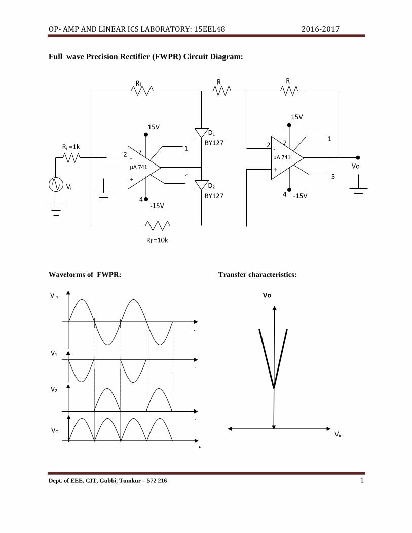
Full wave Precision Rectifier (FWPR) Circuit Diagram:
Waveforms of FWPR: Transfer characteristics:
Rf =10k
Vo
7
4
-
-
+
μA 741
6
5
2
3
15V
1
-15V
-
-
+
μA 741
5
2
3
15V
1
6
-15V
R
10kΩ
R
10kΩ
Rf
10kΩ
Ri =1k
Vi
7
4
D2
BY127
D1
BY127
Vin
t
V2
t
VO
t
V1
t
Vo
Vin

OP- AMP AND LINEAR ICS LABORATORY: 15EEL48 2016-2017
Dept. of EEE, CIT, Gubbi, Tumkur – 572 216 2
Experiment No. : 1 Date: ___/____/_______
FULL WAVE PRECISION RECTIFIERS
Aim : To design full wave precision rectifiers for given specifications and to determine the
performance parameters.
Apparatus :
Sl. No. Particulars Specification Quantity
1. Op-amp A 741 02
2. Diode BY 127 02
3. Resistors As per design -
4. Multimeter 01
5. Adopter 01
6. CRO + Probes 01 Set
7. Spring board + Connecting wires 01 Set
Procedure :
1. Connections are made as shown in circuit diagram.
2. A sinusoidal input of frequency 100Hz and amplitude 0.5V is applied from a function
generator.
3. Rectified output is observed on the CRO. To get equal amplification in both cycles the DC
offset from function generator is carefully adjusted.
4. Input and output voltage levels are noted.
5. A plot of Vo V/S Vi plotted by feeding Vi to channel A and Vo to channel B and time knob to
X via A mode.

OP- AMP AND LINEAR ICS LABORATORY: 15EEL48 2016-2017
Dept. of EEE, CIT, Gubbi, Tumkur – 572 216 3
Design of FWPR:
Specification : For 10VA
110 & 1 , 10f i iChoose R K R K R K
1 2
1
10 1010
1 10
f f
V
i i
R R K KA A A
R R K K
For 1VA ,
Choose Rf = 10kΩ & Ri = 10kΩ
1 2
10 101
10 10
f f
V
i i
R R K KA A A
R R K K
Result :
Tabular column :
Sl. No. Theoretical values of AV Practical values of AV
FWPR:
1.
2.

OP- AMP AND LINEAR ICS LABORATORY: 15EEL48 2016-2017
Dept. of EEE, CIT, Gubbi, Tumkur – 572 216 4

OP- AMP AND LINEAR ICS LABORATORY: 15EEL48 2016-2017
Dept. of EEE, CIT, Gubbi, Tumkur – 572 216 5
Circuit Diagram:
Inverting amplifier:
Non-inverting amplifier:

OP- AMP AND LINEAR ICS LABORATORY: 15EEL48 2016-2017
Dept. of EEE, CIT, Gubbi, Tumkur – 572 216 6
Experiment No. : 2 Date: ___/____/_______
Frequency response of an op – amp amplifier under Inverting and non -
inverting configuration
Aim: To design inverting and non-inverting amplifier for a given gain and analyse the frequency
response of an op-amp amplifier.
Apparatus Required:
Sl.
No. Particulars Range Quantity
1. Op Amp µA741 - 01
2. Resistors As per design -
3. CRO Probes - 03
4. Multi meter - 01
5. Fixed voltage power supply ±15V 01
6. Spring board and connecting wires - -
Procedure:
1. Rig up the circuit as shown in figure.
2. Connect the Vcc, VEE supply as +15V and -15V carefully to the respective pins of the
IC - µA 741
3. Set the suitable frequency & amplitude in the source (Vsin) to get the distortion less output.
Note down the amplitude of the input signal.
4. Keeping the input amplitude constant, Vary the frequency in suitable steps and note down
the corresponding output amplitude.
5. Calculate AV and gain in decibels. Plot a graph of frequency Vs gain in dB. From the graph
calculate f L, f H and band width.

OP- AMP AND LINEAR ICS LABORATORY: 15EEL48 2016-2017
Dept. of EEE, CIT, Gubbi, Tumkur – 572 216 7
Design:
Inverting amplifier:
Given Gain Value ( Av ) =1
Let R1 = 10KΩ
C1=C2=0.1µF
1
2
R
RAv : Therefore R2 = 10KΩ.
Non-inverting amplifier:
Given Av= 2
11
R
RA
f
v
Let R1 = 10KΩ Therefore Rf = 10KΩ
Ideal Graph :
f L = Lower cutoff frequency f H = Higher cutoff frequency

OP- AMP AND LINEAR ICS LABORATORY: 15EEL48 2016-2017
Dept. of EEE, CIT, Gubbi, Tumkur – 572 216 8
Result:
Tabular column:
Vi = ___________ V
F in Hz Vo in Volt AV = Vo / Vi Gain in dB = 20*log AV

OP- AMP AND LINEAR ICS LABORATORY: 15EEL48 2016-2017
Dept. of EEE, CIT, Gubbi, Tumkur – 572 216 9
Circuit Diagram:
RC-PHASE SHIFT OSCILLATOR
Output waveform
Vo
T

OP- AMP AND LINEAR ICS LABORATORY: 15EEL48 2016-2017
Dept. of EEE, CIT, Gubbi, Tumkur – 572 216 10
Experiment No. : 3 Date: __ /__ / _____
RC-Phase Shift Oscillator using Op-Amp
Aim: Design and verify the output waveform of an op – amp RC phase shift oscillator for a desired
Frequency.
Apparatus Required:
Sl.
No. Particulars Range Quantity
1. Op Amp µA741 01
2. Resistors & Capacitors As per design -
3. CRO Probes - 1 Set
4. Multi meter - 01
5. Fixed voltage power supply ±15V 01
6. Spring board and connecting wires - -
Procedure:
1. Components / equipment are tested for their good working condition.
2. Connections are made as shown in the diagram.
3. Dual power supply (15V) is switched ON and feedback resistor Rf is adjusted to get
sustained oscillations.
4. Observe the output wave form on CRO and measure the frequency.
5. Verify the frequency with the designed value.

OP- AMP AND LINEAR ICS LABORATORY: 15EEL48 2016-2017
Dept. of EEE, CIT, Gubbi, Tumkur – 572 216 11
Design:
Result:
fo Theoretical = _____________ Hz
fo Practical = _______________ Hz

OP- AMP AND LINEAR ICS LABORATORY: 15EEL48 2016-2017
Dept. of EEE, CIT, Gubbi, Tumkur – 572 216 12

OP- AMP AND LINEAR ICS LABORATORY: 15EEL48 2016-2017
Dept. of EEE, CIT, Gubbi, Tumkur – 572 216 13
Circuit Diagram:
Wave forms:
Transfer characteristics:

OP- AMP AND LINEAR ICS LABORATORY: 15EEL48 2016-2017
Dept. of EEE, CIT, Gubbi, Tumkur – 572 216 14
Experiment No. : 4 Date: __ /__ / _____
SCHMITT TRIGGER
Aim : To design a Schmitt trigger circuit for the given specifications and hence to plot its output
wave form and transfer characteristics.
Apparatus :
Sl.No. Particulars Range Quantity
1. Op-amp µA741 01
2. Resistors as per design -
3. Multimeter 01
4. Spring board & connecting wires 01 Set
Procedure :
1. Connections are made as shown in the circuit diagram.
2. A sinusoidal input whose amplitude is greater than the magnitude of the UTP & LTP is
applied, a square wave output is obtained and observed on the CRO.
3. UTP & LTP points are noted.
4. To obtain transfer characteristics, input is applied to channel A and output to channel B.
5. UTP & LTP are measured on the transfer characteristics.
Note : The amplitude of the input voltage should be greater than the magnitude of
UTP & LTP level.

OP- AMP AND LINEAR ICS LABORATORY: 15EEL48 2016-2017
Dept. of EEE, CIT, Gubbi, Tumkur – 572 216 15
Design :
Specifications :UTP = 6V, LTP = -2V
1 2
1 2 1 2
1 2
1 2 1 2
6 1
2 2
R sat
R sat
V R V RUTP
R R R R
V R V RLTP
R R R R
2
1 2
1
1 2
1 2 8 2 3
1 2 4 2 4
sat
R
V RUTP LTP
R R
V RUTP LTP
R R
Let Vsat = 12 V & R2 = 10kΩ
kR 20)3( 1
4 3RV V
Result :
Tabular Column:
Sl.
No.
UTP LTP
Theoretical Practical Theoretical Practical
1.
2.
3.
4.
5.

OP- AMP AND LINEAR ICS LABORATORY: 15EEL48 2016-2017
Dept. of EEE, CIT, Gubbi, Tumkur – 572 216 16

OP- AMP AND LINEAR ICS LABORATORY: 15EEL48 2016-2017
Dept. of EEE, CIT, Gubbi, Tumkur – 572 216 17
Circuit Diagram:
(a) Voltage comparator circuit
Wave forms:
(b) Zero crossing detector.
Wave forms:

OP- AMP AND LINEAR ICS LABORATORY: 15EEL48 2016-2017
Dept. of EEE, CIT, Gubbi, Tumkur – 572 216 18
Experiment No. : 5 Date: __ /__ / _____
Voltage comparator and Zero crossing detector
Aim: To verify the operation of an op – amp as voltage comparator and zero crossing detector.
Apparatus:
Sl. No. Particulars Specification Quantity
1. Op-amp µA 741 02
2. Resistors - -
3. Multimeter 01
4. Adopter 01
5. CRO + Probes 01 Set
6. Spring board & connecting wires 01 Set
Procedure:
1. Connect the circuit as shown in the figure
2. Apply the supply voltages of +15V to pin 7 and -15V to pin 4 of IC 741 respectively
from IC Trainer kit. Connect the ground to the ground point.
3. Set the reference voltage as 1V DC.
4. Apply sine wave of 10Vp-p with1KHz frequency from the function generator as Vi.
5. Check the output in CRO and calculate the amplitude of the output wave form.
6. Compare the output wave form amplitude with input signal amplitude.
Result:
Vref(V) Vi (V) Vo(V)

OP- AMP AND LINEAR ICS LABORATORY: 15EEL48 2016-2017
Dept. of EEE, CIT, Gubbi, Tumkur – 572 216 19
Circuit Diagram:
(a) ADDER
Design: Rf = 10k R1 = R2 = 10k
If R1 = R2 = Rf = R, then
V0 = - (V1 + V2)
(b) Subtractor
Design: Rf & R = 10k , R1 & R2 = 10k
If Rf = R1 = R2 = R, then V0 = V2 - V1
Vo = V2 – V1

OP- AMP AND LINEAR ICS LABORATORY: 15EEL48 2016-2017
Dept. of EEE, CIT, Gubbi, Tumkur – 572 216 20
Experiment No. : 6 Date: __ /__ / _____
Verify the operation of op – amp as an adder, subtractor, integrator and
differentiator
Aim: Design and verify the operation of op – amp as an adder, sub tractor, integrator and differentiator.
Apparatus:
Sl. No. Particulars Specification Quantity
1. Op-amp µA 741 02
2. Resistors As per design -
3. Multimeter 01
4. CRO + Probes 01 Set
5. Spring board & connecting wires 01 Set
PROCEDURE:
1. Connections are made as shown in the circuit diagram.
2. Apply AC input signal to the input terminals of an op-amp.
3. By adjusting the amplitude and frequency knobs of the function generator, appropriate
input voltage is applied to the inverting input terminal of the Op-Amp.
4. Observe the output wave forms on CRO.
5. Measure the DC output voltage using multimeter.

OP- AMP AND LINEAR ICS LABORATORY: 15EEL48 2016-2017
Dept. of EEE, CIT, Gubbi, Tumkur – 572 216 21
C. Integrator
Design:
Given: Triangular output waveform with a peak-to-peak amplitude of 4 V
The input is a ±5 V square wave with a frequency of 500 Hz
C1=0.1 µF
msf
Tt 1
2
1
2
Vv 4
At
vCI 4001
1
KI
VR i 5.12
400
5
1
1
R2=20R1=250 KΩ (270KΩ)
R3=R1
OP- AMP AND LINEAR ICS LABORATORY: 15EEL48 2016-2017
Dept. of EEE, CIT, Gubbi, Tumkur – 572 216 22
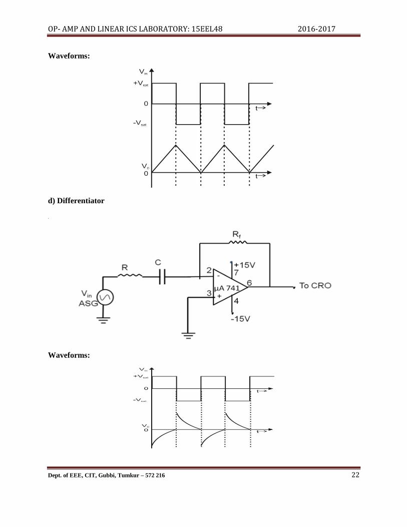
Waveforms:
d) Differentiator
.
Waveforms:

OP- AMP AND LINEAR ICS LABORATORY: 15EEL48 2016-2017
Dept. of EEE, CIT, Gubbi, Tumkur – 572 216 23
Design:
Design a differentiating circuit to give an output of 5V when input changes by 1V in a time of 100 µs.Use
an op-amp with a bipolar input stage.
I1 ≥≥ IB(max)
I1=500 µA
KI
VR 10
500
5
1
02
FV
tIC 05.01
1
50020
21
RR
R3=R2
VCC ≥ ±(V0+3V)
Result:
Tabular Column:
V1 V2 Vo theoretical Vo practical
Adder
Subtractor

OP- AMP AND LINEAR ICS LABORATORY: 15EEL48 2016-2017
Dept. of EEE, CIT, Gubbi, Tumkur – 572 216 24
Integrator:
Input- Square wave Output -Triangular wave
Amplitude Time period Amplitude Time period
Input-Sine wave Output -Cosine wave
Amplitude Time period Amplitude Time period
Differentiator:
Input- square wave Output -Spikes
Amplitude Time period Amplitude Time period
Input- sine wave Output -cosine
Amplitude Time period Amplitude Time period
OP- AMP AND LINEAR ICS LABORATORY: 15EEL48 2016-2017
Dept. of EEE, CIT, Gubbi, Tumkur – 572 216 25
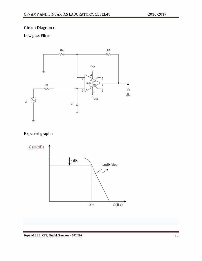
Circuit Diagram :
Low pass Filter
Expected graph :

OP- AMP AND LINEAR ICS LABORATORY: 15EEL48 2016-2017
Dept. of EEE, CIT, Gubbi, Tumkur – 572 216 26
Experiment No. : 7 Date: ___/____/_______
FIRST ORDER BUTTER WORTH ACTIVE LOW PASS &
HIGH PASS FILTER
Aim: To conduct an experiment to study the frequency response of an 1st order active Low
Pass and High Pass Filter.
Apparatus:
Sl.No. Particulars Range Quantity
1. Op-amp μA 741 01
2. Resistors & Capacitors As per design 04
3. CRO + Probes - 01 set
4. Adaptor - 01
5. Spring board + connecting wires - 01 set
Procedure:
1. Check the components/Equipments for their working condition.
2. Connections are made as shown in the circuit diagram.
3. Apply sine eave signal of amplitude 5V peak to peak(approximately).
4. Vary the frequency and note down the corresponding output amplitude.
5. Tabulate the readings and plot a graph of frequency Vs Gain in dB.

OP- AMP AND LINEAR ICS LABORATORY: 15EEL48 2016-2017
Dept. of EEE, CIT, Gubbi, Tumkur – 572 216 27
Design :
Specification : Pass Band Gain (Av ) = 1.586
Cut-off frequency fH = 5kHz
) 1
10
101.586 1 17.064
f
V
A
f
A
A
Ri A
R
Assume R K
KR K
R
fH = 1 / (2RC)
Assume C = 0.1µF Then 3 6
1 1318 330
2 2 5 10 0.1 10H
R Use stdf C X X X X
R1 = R = 318 Ω
Tabular Column :
Vi = _______________ V
f in Hz Vo in Volt Av = Vo / Vi
Gain in dB = 20 Log
Av

OP- AMP AND LINEAR ICS LABORATORY: 15EEL48 2016-2017
Dept. of EEE, CIT, Gubbi, Tumkur – 572 216 28
High pass Filter
Expected graph :
3dB
+20dB/dec Gain(dB)
fL f (Hz)

OP- AMP AND LINEAR ICS LABORATORY: 15EEL48 2016-2017
Dept. of EEE, CIT, Gubbi, Tumkur – 572 216 29
Design :
Specifications : Pass Band Gain (Av ) = 1.586
Cut-off frequency fL = 5kHz
) 1
10
101.586 1 17.064
f
V
A
f
A
A
Ri A
R
Assume R K
KR K
R
The cutoff frequency fL = 1 / (2RC)
Assume C = 0.1µF Then
3 6
1 1318 330
2 2 5 10 0.1 10L
R Use stdf C X X X X
R1 = R = 318 Ω
Tabular Column :
Vi = _____________ V
f in Hz Vo in Volt Av = Vo / Vi Gain in dB = 20 Log (Av)

OP- AMP AND LINEAR ICS LABORATORY: 15EEL48 2016-2017
Dept. of EEE, CIT, Gubbi, Tumkur – 572 216 30
Band pass filter
Expected graph :
3dB
-20dB/dec
fL fH f (Hz)
B.W
+20
dB/dec
Gain (dB)

OP- AMP AND LINEAR ICS LABORATORY: 15EEL48 2016-2017
Dept. of EEE, CIT, Gubbi, Tumkur – 572 216 31
Design :
Specification : Pass Band Gain ( Av ) = 1.586
Cutoff frequencies f L = 5 kHz, f H = 8 kHz, Bandwidth = 3 kHz
i) 1f
V
A
RA
R
1010 1.586 1 17.064f A
A
KAssume R K Then R K
R
ii) LPF:
The cutoff frequency fH = 1 / (2RaCa)
Assume Ca = 0.1µF Then
3 6
1 1198 220
2 2 8 10 0.1 10a
H
R Use stdf C X X X X
iii) HPF:
The cutoff frequency fL = 1 / (2RbCb)
Assume Cb = 0.1µF Then
3 6
1 1318 330
2 2 5 10 0.1 10b
L
R Use stdf C X X X X

OP- AMP AND LINEAR ICS LABORATORY: 15EEL48 2016-2017
Dept. of EEE, CIT, Gubbi, Tumkur – 572 216 32
Tabular Column :
For BPF: Vi = ____________ V
f in Hz Vo in Volt Av = Vo / Vi Gain in dB = 20 Log Av
Result:
Low Pass Filter : Cut off frequency, fH Theoretical = _________
Cut off frequency, fH Practical = _________
Pass band gain Av Theoretical = _________
Pass band gain Av Practical = _________
Roll off Theoretical = _________
Roll off Practical = _________
Band Pass Filter:
Cut off frequency, fH Theoretical = _________
Cut off frequency, fH Practical = _________
Cut off frequency, fL Theoretical = _________
Cut off frequency, fL Practical = _________
Pass band gain Av Theoretical = _________
Pass band gain Av Practical = _________
Roll off Theoretical = _________
Roll off Practical = _________
Bandwidth Theoretical = _________
Bandwidth Practical = _________
High Pass Filter : Cut off frequency, fL Theoretical = _________
Cut off frequency, fL Practical = _________
Pass band gain Av Theoretical = _________
Pass band gain Av Practical = _________
Roll off Theoretical = _________
Roll off Practical = _________

OP- AMP AND LINEAR ICS LABORATORY: 15EEL48 2016-2017
Dept. of EEE, CIT, Gubbi, Tumkur – 572 216 33
Circuit Diagram :
OP-amp based function generator to generate sine, triangular & square waveforms
Wave forms:

OP- AMP AND LINEAR ICS LABORATORY: 15EEL48 2016-2017
Dept. of EEE, CIT, Gubbi, Tumkur – 572 216 34
Experiment No. : 8 Date: ___/____/_______
Function generator using op-amp
Aim: To generate sine, triangular & square waveforms & to determine the Frequency of oscillations.
Apparatus:
Sl.No. Particulars Range Quantity
1. Op-amp LM 324 01
2. Resistors & Capacitors As per design
3. CRO + Probes - 01 set
4. Fixed voltage power supply ±15V 01
5. Spring board + connecting wires - 01 set
Procedure:
1. Connect the circuit as per the circuit diagram shown in Fig.
2. Vary the pot & observe the output on the CRO.
3. Calculate theoretical and practical output signal frequency and compare them.
Result:

OP- AMP AND LINEAR ICS LABORATORY: 15EEL48 2016-2017
Dept. of EEE, CIT, Gubbi, Tumkur – 572 216 35
Circuit diagram:
Design :
Specification:
Design a 4 bit R-2R DAC for an output voltage, V0 = 5V, when the input is 10V. (i.e.,
binary no. 1010).
D3 D2 D1 D0
( 10 )10 = ( 1 0 1 0 ) 2
Therefore D3 = 1 (MSB), D2 = 0, D1 = 1, D0 = 0 (LSB)
1 2
1 2 3
1
1
2 4 816
55 0 2 0 8
16
85 8
5
f foV o V i V
i
f ref
o o
f
f
f
R RV KA V A V A A A
V R K R
R VV D D D D
R
R
R
RR R
R
5 & 2 10
8f
Let R K R K
R K

OP- AMP AND LINEAR ICS LABORATORY: 15EEL48 2016-2017
Dept. of EEE, CIT, Gubbi, Tumkur – 572 216 36
Experiment No. : 9 Date: ___/____/_______
4-BIT R-2R DIGITAL TO ANALOG CONVERTER
Aim : To design 4 bit R-2R ladder DAC using Op-Amp for an output voltage of 5 V when the
input is 10 (Binary 1010).
Apparatus :
Sl.
No. Particulars Specification Quantity
1. IC µA741 02
2. Resistors As per design -
3. Multimeter - 01
4. Base board + connecting wires - 01 Set
Procedure :
1. Connections are made as shown in the circuit diagram.
2. Digital input data is given at D3, D2, D1, D0 and corresponding analog output voltage V0 is
measured.
3. Tabulate the readings & plot the graph between Vo on y-axis Vin on X-axis.
Note :
1. D0.D1.D2 & D3 are binary input.
2. Vo is the analog output.
3. Binary inputs Do.D1.D2 & D3 can take either the value ‘0’ or ‘1’.
4. Binary input Di (i = 0 to 3) can be made ‘0’ by connecting the i/p to ground. It can be made
‘1’ by connecting to –5 V.
Logic 0 0V
Logic 1 +5V

OP- AMP AND LINEAR ICS LABORATORY: 15EEL48 2016-2017
Dept. of EEE, CIT, Gubbi, Tumkur – 572 216 37
The output voltage is proportional to the relation below
refo
o VdDDD
V
4
3
3
2
2
1
1
0
2
2222
Result :
Decimal
Value
Binary Inputs Analog O/P
Vo(volts)
Theoretical values
Analog O/P
Vo(volts)
Practical values D3 D2 D1 D0
0 0 0 0 0
1 0 0 0 1
2 0 0 1 0
3 0 0 1 1
4 0 1 0 0
5 0 1 0 1
6 0 1 1 0
7 0 1 1 1
8 1 0 0 0
9 1 0 0 1
10 1 0 1 0
11 1 0 1 1
12 1 1 0 0
13 1 1 0 1
14 1 1 1 0
15 1 1 1 1
OP- AMP AND LINEAR ICS LABORATORY: 15EEL48 2016-2017
Dept. of EEE, CIT, Gubbi, Tumkur – 572 216 38
OP- AMP AND LINEAR ICS LABORATORY: 15EEL48 2016-2017
Dept. of EEE, CIT, Gubbi, Tumkur – 572 216 39
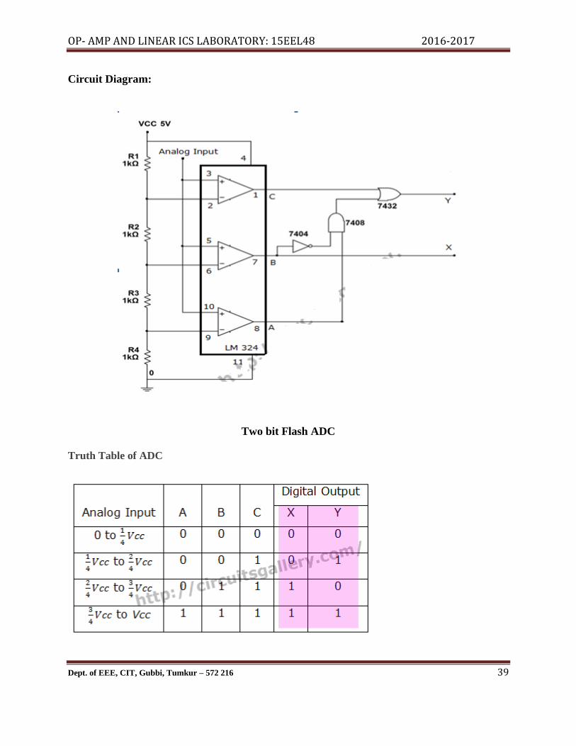
Circuit Diagram:
Two bit Flash ADC
Truth Table of ADC

OP- AMP AND LINEAR ICS LABORATORY: 15EEL48 2016-2017
Dept. of EEE, CIT, Gubbi, Tumkur – 572 216 40
Experiment No. : 10 Date: ___/____/_______
Realization of two bit Flash ADC
Aim : To realize two bit Flash ADC
Apparatus :
Sl.
No. Particulars Specification Quantity
1. IC
LM324
7404
7432
7409
04
2. Resistors 1K 04
3. Multimeter - 01
4. Base board + connecting wires - 01 Set
Procedure :
1. Connections are made as shown in the circuit diagram.
2. Apply the different analog input voltages and note down the output.
Result:

OP- AMP AND LINEAR ICS LABORATORY: 15EEL48 2016-2017
Dept. of EEE, CIT, Gubbi, Tumkur – 572 216 41
Circuit Diagram :
Monostable multivibrator
Design :
Specification : output pulse width =Delay time =0.5 ms
Output delay time 1.1d AT R C
Let RA = 10 K Then
0.045 0.047 standard r1.1
d
A
TC F Use F capacito
R
Here 2
upper threshold voltage3
UT CCV V
Choose T T dR C T
Select 10
dT T
TR C
Output duty cycle 1
Input trigger pulse frequencydTd f
T T
Adjust input frequency ‘f ’ from the pulse generator to f = 1KHz
i.e., T = 1ms (i.e., twice the output delay time

OP- AMP AND LINEAR ICS LABORATORY: 15EEL48 2016-2017
Dept. of EEE, CIT, Gubbi, Tumkur – 572 216 42
Experiment No. : 11 Date: ___/____/_______
IC 555 timer based pulse generator for the specified pulse
Aim: To design and verify an IC 555 timer based pulse generator for the specified pulse
Apparatus :
Sl.No. Particulars Range Quantity
1. IC 555 timer 01
2. Resistors & Capacitors As per design -
3. Diode BY127 02
4. Spring board + connecting wires - 01 set
Procedure:
1. Check the components/Equipments for their working condition.
2. Connections are made as shown in the circuit diagram.
3. Switch on the power supply and observe the output waveforms on CRO and measure Td
value and verify with the designed value.
4. observe the waveforms at different points as shown in the waveforms.
Result :
MULTIVIBRATORS Ton Toff Td
Monostable

OP- AMP AND LINEAR ICS LABORATORY: 15EEL48 2016-2017
Dept. of EEE, CIT, Gubbi, Tumkur – 572 216 43
Expected waveforms :

OP- AMP AND LINEAR ICS LABORATORY: 15EEL48 2016-2017
Dept. of EEE, CIT, Gubbi, Tumkur – 572 216 44

OP- AMP AND LINEAR ICS LABORATORY: 15EEL48 2016-2017
Dept. of EEE, CIT, Gubbi, Tumkur – 572 216 45
Circuit diagram:

OP- AMP AND LINEAR ICS LABORATORY: 15EEL48 2016-2017
Dept. of EEE, CIT, Gubbi, Tumkur – 572 216 46
Experiment No. : 12 Date: ___/____/_______
Designing of Fixed voltage power supply using IC regulators
Aim: To design & construct regulated power supply using IC regulators 78 and 79 series
APPARATUS REQUIRED:
SL no Apparatus Range Quantity
1 Diode(BY127) - 4
2 Resistor 1KΩ 1 each
3 Step down Transformer 12-0-12 1
4 CRO - 1
5 Probes - 1set
6 Capacitors 1000µF 2
PROCEDURE:
1. Rig up the circuits as shown in the Circuit diagram.
2. Apply 230V, 50Hz input to primary of the transformer.
3. Observe the rectified output waveform across the load resistance RL.
4. Using multimeter measure voltage across resistors(V01 & V02).
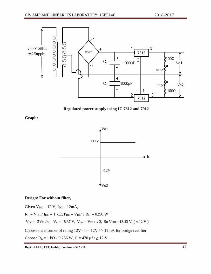
OP- AMP AND LINEAR ICS LABORATORY: 15EEL48 2016-2017
Dept. of EEE, CIT, Gubbi, Tumkur – 572 216 47
Regulated power supply using IC 7812 and 7912
Graph:
Design: For without filter,
Given VDC = 12 V, IDC = 12mA,
RL = VDC / IDC = 1 k, PRL = VDC2 / RL = 0256 W
VDC = 2Vm/π , Vm = 18.37 V, Vrms = Vm / 2, So Vrms=13.43 V, ( 12 V )
Choose transformer of rating 12V - 0 – 12V / ≥ 12mA for bridge rectifier
Choose RL = 1 k / 0.256 W, C = 470 f / ≥ 12.V
IL
Vo1
Vo2
+12V
-12V

OP- AMP AND LINEAR ICS LABORATORY: 15EEL48 2016-2017
Dept. of EEE, CIT, Gubbi, Tumkur – 572 216 48
Design:(Additional calculation for with filter),
Given VDC = 12 V, IDC = 12ma, =0.006,
From = 1 / ( 4 3 fCRL ), C = 481 f, ( 470f ) ( f = 50 Hz )
Result:
Tabular Column:
Vdc Vrpp Vrrms=Vrpp / 2 3 V01 V02
OP- AMP AND LINEAR ICS LABORATORY: 15EEL48 2016-2017
Dept. of EEE, CIT, Gubbi, Tumkur – 572 216 49
REFERENCES
1. Op-Amps and Linear Integrated Circuits by Ramakant A Gayakwad, Pearson Publications, 4th
Edition 2015.
2.Operational Amplifiers and Linear ICs by David A. Bell Oxford University Press publications,
3rd Edition 2011.
3. Linear Integrated Circuits; Analysis, Design and Applications by B. Somanthan Nair, Wiley
India Publications, 2013.
4. Linear Integrated Circuits by S. Salivahanan, etal, Mc Graw Hill publications, 2nd Edition,
2014.
5. Operational Amplifiers and Linear Integrated Circuits K. Lal Kishore Pearson publications, 1st
Edition, 2012.
6.Linear Integrated Circuits by Muhammad H Rashid, Cengage Learning publications, 1st
Edition,2014.
7.Op-Amps and Linear Integrated Circuits, Concept and Application by James M Fiore, Cengage
publications, 2009.

OP- AMP AND LINEAR ICS LABORATORY: 15EEL48 2016-2017
Dept. of EEE, CIT, Gubbi, Tumkur – 572 216 50
VIVA QUESTIONS
1. What is Op-amp? What are the ideal characteristics of op-amp.
2. Give the practical values of voltage gain, Zin, Zout of an op-amp.
3. What is meant by CMRR? What is its significance.
4. Why gain of op-amp should be infinite.
5. What is slew rate, output offset voltage.
6. What is meant by maximum output voltage swing.
7. What is meant by inverting amplifier.
8. What is meant by non-inverting amplifier.
9. What is a voltage follower? How do you realize a voltage follower.
10. What is a comparator?
11. Why the output of comparator is always square wave.
12. Which circuit is called regenerative comparator and why.
13. What is trip point in comparator?
14. What are the limitations of comparator?
15. What is the condition for the circuit to work as integrator and differentiator.
16. What is ZCD and give one of its applications?
17. What is summer.
18. What is Schmitt Trigger.
19. Explain the working of Schmitt trigger.
20. What is meant by UTP and LTP.
21. Define Dead band or Dead zone.
22. Mention the applications of Schmitt Trigger.
23. Define Rectifier.
24. Name the types of Rectifier.
25. What is Precision Rectifier.
26. Realize the rectifier circuits using diodes.
27. Mention types of precision rectifier.
28. Explain the working of Full Wave Precision Rectifier.
29. Define Conversion.

OP- AMP AND LINEAR ICS LABORATORY: 15EEL48 2016-2017
Dept. of EEE, CIT, Gubbi, Tumkur – 572 216 51
30. Different types of D/A Converter.
31. Working of R-2R D/A Converter.
32. What do you understand by DAC and ADC? Where is it used.
33. What is advantage of R-2R DAC over other type DAC.
34. What is resolution (step size) in a DAC.
35. What is offset error in a DAC.
36. What are the different types of ADC.
37. Which is the fastest ADC? What are its limitations.
38. Which is the most commonly used ADC.
39. What is a filter.
40. Distinguish between active and passive filters.
41. Distinguish between analog and digital filters.
42. What are the advantages of active filters over passive filters.
43. Explain the classification of filters.
44. Define low pass filter.
45. Define high pass filter.
46. Why inductors are not often used in filters.
47. What are the applications of filters.
48. Mention some of the linear applications of op–amps
49. Mention some of the non – linear applications of op-amps?
50. What happens when the common terminal of V+ and V- sources is not grounded?
51. What is a comparator?
52. Explain barkhausen criterion for oscillations?
53. What is a voltage regulator?
54. What are the advantages of IC voltage regulators?

OP- AMP AND LINEAR ICS LABORATORY: 15EEL48 2016-2017
Dept. of EEE, CIT, Gubbi, Tumkur – 572 216 52
Qusetion Bank
1. Design a schmitt trigger circuit for the given values of UTP = ____V & LTP = ____V and
draw the relevant waveforms.
2. Design a 4-bit R-2R ladder DAC to give an analog output voltage of ____ V when the
digital input voltage is ____ V.
3. Conduct an experiment on full wave precision rectifier for a given gain _______.
4. Design a first order butter worth active low pass filter for a given cutoff frequency fc =
_______KHz (<10KHz) .
5. Design a first order butter worth active high pass filter for a given cutoff frequency fc =
______KHz (<10KHz.
6. Design a first order butter worth active band pass filter for a given cutoff frequency fh =
______ KHz and fl = ______KHz.
7. Design a Monostable multivibrator for a given pulse width _________.
8. Design and realize an op – amp based function generator to generate sine, square and
triangular waves of desired frequency.
9. Realize two bit Flash ADC.
10. Design and verify an IC 555 timer based pulse generator for the specified pulse.
11. Design a Fixed voltage power supply using IC regulators 78 series and 78 series.
12. Design and verify the operation of op – amp as an (a) adder (b) subtractor (c) integrator and
(d)differentiator.
13. Verify the operation of an op – amp as (a) voltage comparator circuit and (b) zero crossing
detector.
14. Design and verify the output waveform of an op – amp RC phase shift oscillator for a desired
frequency.
15.Design and realize to analyse the frequency response of an op – amp amplifier under
Inverting and non - inverting configuration for a given gain.
OP- AMP AND LINEAR ICS LABORATORY: 15EEL48 2016-2017
Dept. of EEE, CIT, Gubbi, Tumkur – 572 216 53
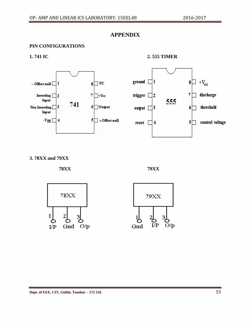
APPENDIX
PIN CONFIGURATIONS
1. 741 IC 2. 555 TIMER
3. 78XX and 79XX
78XX 79XX

OP- AMP AND LINEAR ICS LABORATORY: 15EEL48 2016-2017
Dept. of EEE, CIT, Gubbi, Tumkur – 572 216 54
IC LM324
Single Supply Quad Operational Amplifiers