lab4 nmos.cir * lab4 nmos.cir - pspice...
TRANSCRIPT

ECE3204 Lab 4 Sample-‐and-‐Hold Circuit Simulations Page 1
M:\Courses\ece3204\3204_pspice\lab4_NMOS.cir
* lab4_NMOS.cir - pSpice example* Show V-I characteristics for MOSFETs
* N-channel MOSFETM1 vd vg 0 0 MC14007N
* VGSVGS vg 0 DC 5
* VDSVDS vd 0 DC 5
* MOSFET models (See ECE4902 for meaning of parameters).model MC14007N NMOS LEVEL=3 W=350u L=10u VTO= 1.5 UO=600 TOX=1E-7 NSUB=1E+15.model MC14007P PMOS LEVEL=3 W=900u L=10u VTO=-1.5 UO=200 TOX=1E-7 NSUB=3E+15
* DC Analysis* Sweep VDS at each value of VGS.dc VDS 0 15 0.01
* Different values of VGS.STEP VGS 0 5 1
* Write .dat file for use by probe.probe
Page: 1
Date/Time run: 11/28/11 09:49:14* lab4_NMOS.cir - pSpice example
Temperature: 27.0
Date: November 28, 2011 Page 1 Time: 09:50:38
(Q) lab4_NMOS (active)
VDS
0V 2V 4V 6V 8V 10V 12V 14V 15VID(M1)
0A
2.5mA
5.0mA
ECE3204 Lab 4 Sample-‐and-‐Hold Circuit Simulations Page 2
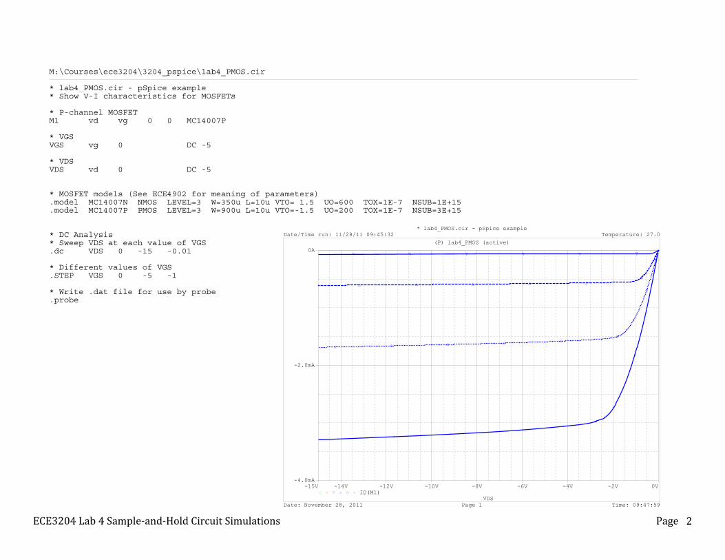
M:\Courses\ece3204\3204_pspice\lab4_PMOS.cir
* lab4_PMOS.cir - pSpice example* Show V-I characteristics for MOSFETs
* P-channel MOSFETM1 vd vg 0 0 MC14007P
* VGSVGS vg 0 DC -5
* VDSVDS vd 0 DC -5
* MOSFET models (See ECE4902 for meaning of parameters).model MC14007N NMOS LEVEL=3 W=350u L=10u VTO= 1.5 UO=600 TOX=1E-7 NSUB=1E+15.model MC14007P PMOS LEVEL=3 W=900u L=10u VTO=-1.5 UO=200 TOX=1E-7 NSUB=3E+15
* DC Analysis* Sweep VDS at each value of VGS.dc VDS 0 -15 -0.01
* Different values of VGS.STEP VGS 0 -5 -1
* Write .dat file for use by probe.probe
Page: 1
Date/Time run: 11/28/11 09:45:32* lab4_PMOS.cir - pSpice example
Temperature: 27.0
Date: November 28, 2011 Page 1 Time: 09:47:59
(P) lab4_PMOS (active)
VDS
-14V -12V -10V -8V -6V -4V -2V 0V-15VID(M1)
-4.0mA
-2.0mA
0A
ECE3204 Lab 4 Sample-‐and-‐Hold Circuit Simulations Page 3
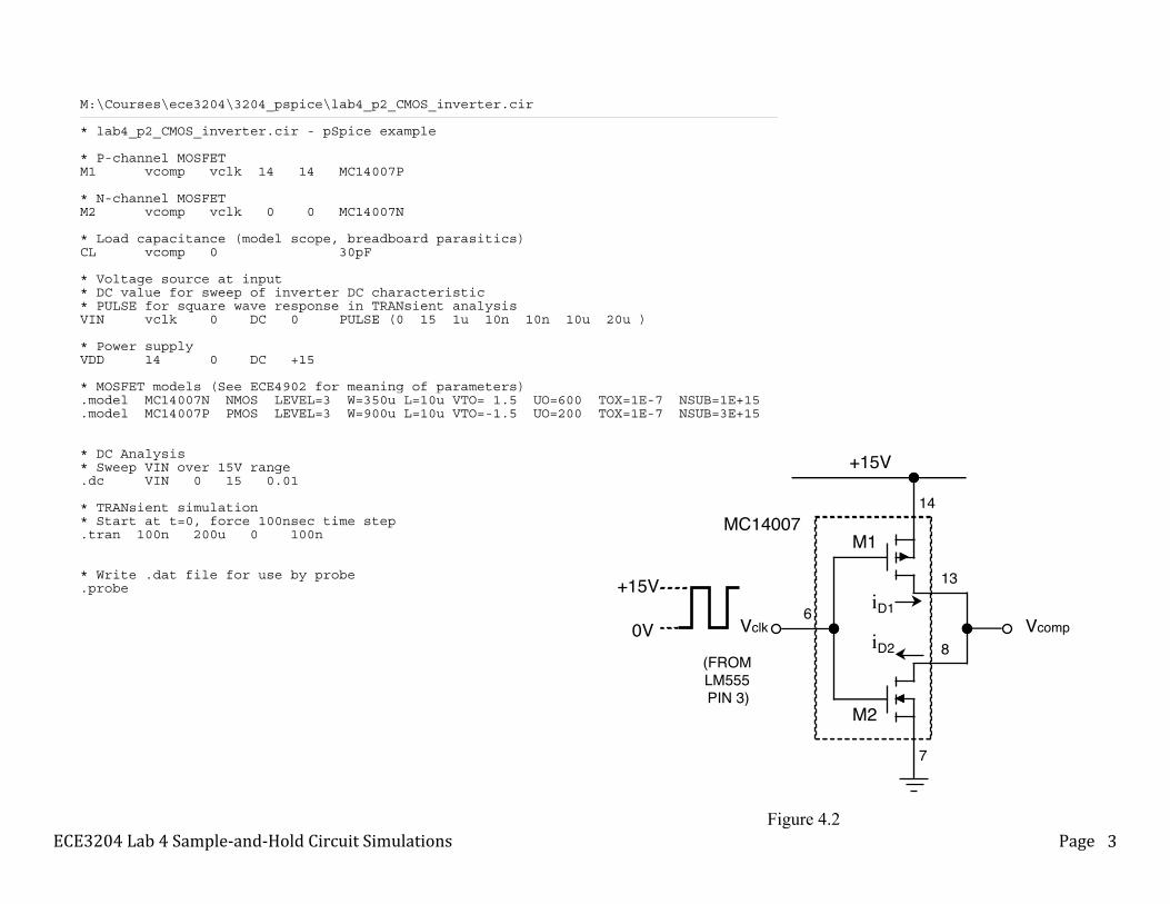
M:\Courses\ece3204\3204_pspice\lab4_p2_CMOS_inverter.cir
* lab4_p2_CMOS_inverter.cir - pSpice example
* P-channel MOSFETM1 vcomp vclk 14 14 MC14007P
* N-channel MOSFETM2 vcomp vclk 0 0 MC14007N
* Load capacitance (model scope, breadboard parasitics)CL vcomp 0 30pF
* Voltage source at input* DC value for sweep of inverter DC characteristic* PULSE for square wave response in TRANsient analysisVIN vclk 0 DC 0 PULSE (0 15 1u 10n 10n 10u 20u )
* Power supplyVDD 14 0 DC +15
* MOSFET models (See ECE4902 for meaning of parameters).model MC14007N NMOS LEVEL=3 W=350u L=10u VTO= 1.5 UO=600 TOX=1E-7 NSUB=1E+15.model MC14007P PMOS LEVEL=3 W=900u L=10u VTO=-1.5 UO=200 TOX=1E-7 NSUB=3E+15
* DC Analysis* Sweep VIN over 15V range.dc VIN 0 15 0.01
* TRANsient simulation* Start at t=0, force 100nsec time step.tran 100n 200u 0 100n
* Write .dat file for use by probe.probe
Page: 1
2
P2. CMOS Inverter
The digital output Vclk of the LM555 timer will swing from its negative to positive supply: ground to +15V. The 2:1 multiplexer will require Vclk and its complement Vcomp. To generate the complement signal, we will be using a digital inverter constructed of two transistors from the MC14007 MOSFET array, as shown in Figure 4.2.
P2.1 Explain how the circuit of Figure 4.2 produces the logic complement of Vclk at Vcomp.
One advantage of CMOS logic is its low power dissipation.
P2.2 Consider the drain currents iD1 and iD2 flowing in the transistors M1 and M2. Assuming there is no load on Vcomp, what are the approximate drain currents when Vclk is high? When Vclk is low? When does a significant amount of drain current flow?
P2.3 Sketch Vcomp when Vclk is driven from pin 3 of the LM555 circuit you designed in part P1.2.
7
13
8
+15V
14
VcompVclk6
0V
+15V
(FROMLM555PIN 3)
MC14007
iD1
iD2
M1
M2
Figure 4.2
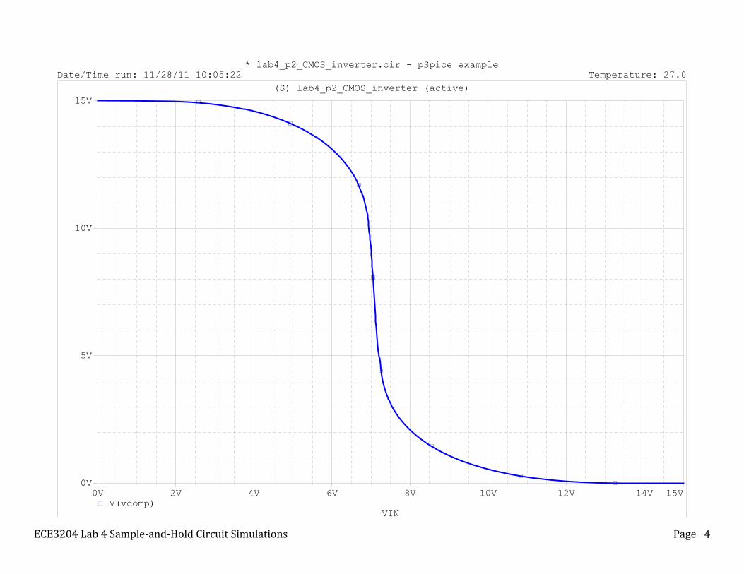
ECE3204 Lab 4 Sample-‐and-‐Hold Circuit Simulations Page 4
Date/Time run: 11/28/11 10:05:22* lab4_p2_CMOS_inverter.cir - pSpice example
Temperature: 27.0
Date: November 28, 2011 Page 1 Time: 10:06:29
(S) lab4_p2_CMOS_inverter (active)
VIN
0V 2V 4V 6V 8V 10V 12V 14V 15VV(vcomp)
0V
5V
10V
15V

ECE3204 Lab 4 Sample-‐and-‐Hold Circuit Simulations Page 5
Date/Time run: 11/28/11 10:05:22* lab4_p2_CMOS_inverter.cir - pSpice example
Temperature: 27.0
Date: November 28, 2011 Page 1 Time: 10:09:14
(T) lab4_p2_CMOS_inverter (active)
Time
0s 20us 40us 60us 80us 100us 120us 140us 160us 180us 200usV(vcomp)
5V
10V
15V
-1VSEL>>
V(vclk)
0V
5V
10V
15V

ECE3204 Lab 4 Sample-‐and-‐Hold Circuit Simulations Page 6
Date/Time run: 11/28/11 10:11:08* lab4_p2_CMOS_inverter.cir - pSpice example
Temperature: 27.0
Date: November 28, 2011 Page 1 Time: 10:13:10
(U) lab4_p2_CMOS_inverter (active)
Time
0.996us 1.000us 1.004us 1.008us 1.012us 1.016us 1.020us 1.024usV(vcomp)
0V
5V
10V
15V
V(vclk)
5V
10V
15V
-1VSEL>>
ECE3204 Lab 4 Sample-‐and-‐Hold Circuit Simulations Page 7
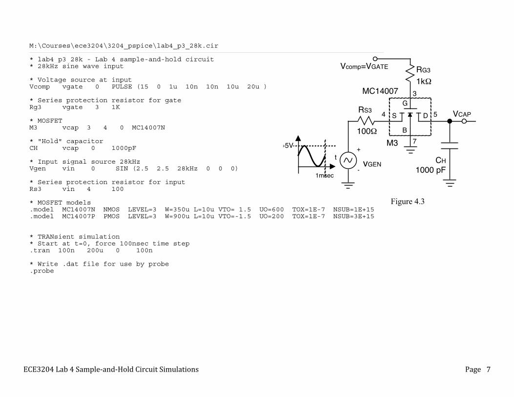
M:\Courses\ece3204\3204_pspice\lab4_p3_28k.cir
* lab4_p3_28k - Lab 4 sample-and-hold circuit* 28kHz sine wave input
* Voltage source at inputVcomp vgate 0 PULSE (15 0 1u 10n 10n 10u 20u )
* Series protection resistor for gateRg3 vgate 3 1K
* MOSFETM3 vcap 3 4 0 MC14007N
* "Hold" capacitorCH vcap 0 1000pF
* Input signal source 28kHzVgen vin 0 SIN (2.5 2.5 28kHz 0 0 0)
* Series protection resistor for inputRs3 vin 4 100
* MOSFET models.model MC14007N NMOS LEVEL=3 W=350u L=10u VTO= 1.5 UO=600 TOX=1E-7 NSUB=1E+15.model MC14007P PMOS LEVEL=3 W=900u L=10u VTO=-1.5 UO=200 TOX=1E-7 NSUB=3E+15
* TRANsient simulation* Start at t=0, force 100nsec time step.tran 100n 200u 0 100n
* Write .dat file for use by probe.probe
Page: 1
3
P3. Sample-and-hold
The sample and hold circuit of Figure 4.3 uses one of the MC14007 N-channel MOSFETs as analog switch M3. Note that VGEN is a 1kHz, 5V peak-to-peak sine wave with a +2.5V DC offset: the voltage swings from 0V to +5V. Resistors RG3 and RS3 are for protection of the analog switch.
P3.1 Show that when VGATE = +15V, the analog switch is conducting and VCAP ! VGEN for VGEN, 0V " VGEN " +5V.
P3.2 Show that when VGATE = 0V, the analog switch is off and the voltage at VCAP will remain constant, holding its previous value when VGATE transitioned to 0V.
P3.3 Sketch VGATE and the sample-and-hold output VHOLD when the gate is driven from Vcomp of section P2.3, and VGEN is as shown.
P3.4 If VGEN were to go to a voltage of -5V, what would happen in the analog switch MOSFET M3? (Hint: consider the role of the substrate/body (B) terminal of the MOSFET)
VHOLD
CH1000 pF
VCAP
M3
Vcomp=VGATE
vGEN
+
-
100!
RS3
RG3
1k!
G
B
S D
3
7
54
MC14007
3
26
7
4
+15V
-15V
LF356
t+5V
1msec
Figure 4.3

ECE3204 Lab 4 Sample-‐and-‐Hold Circuit Simulations Page 8
Date/Time run: 11/28/11 10:17:46* Title here - lab4_P3_28k - pSpice example
Temperature: 27.0
Date: November 28, 2011 Page 1 Time: 10:20:41
(W) lab4_p3_28k (active)
Time
0s 20us 40us 60us 80us 100us 120us 140us 160us 180us 200usV(vcap) V(vin)
2.5V
5.0V
-0.1VSEL>>
V(vgate)
0V
5V
10V
15V
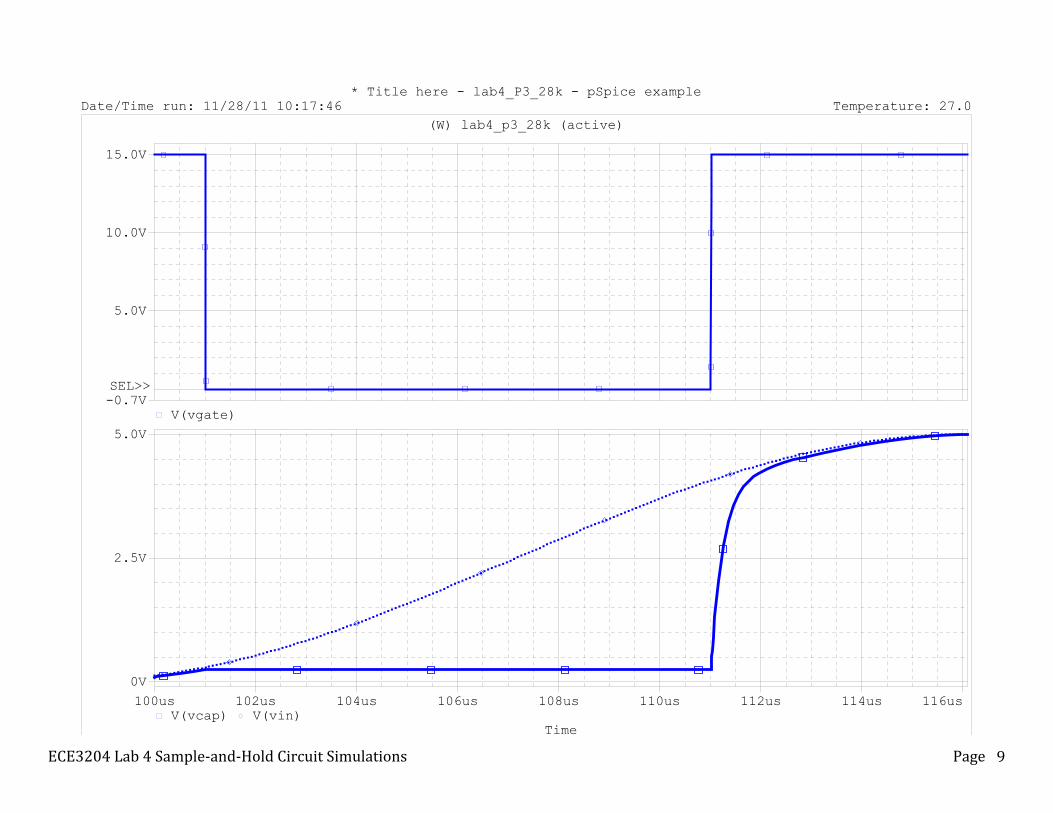
ECE3204 Lab 4 Sample-‐and-‐Hold Circuit Simulations Page 9
Date/Time run: 11/28/11 10:17:46* Title here - lab4_P3_28k - pSpice example
Temperature: 27.0
Date: November 28, 2011 Page 1 Time: 10:22:01
(W) lab4_p3_28k (active)
Time
100us 102us 104us 106us 108us 110us 112us 114us 116usV(vcap) V(vin)
0V
2.5V
5.0VV(vgate)
5.0V
10.0V
15.0V
-0.7VSEL>>

ECE3204 Lab 4 Sample-‐and-‐Hold Circuit Simulations Page 10
Date/Time run: 11/28/11 10:30:05* lab4_p3_28k - Lab 4 sample-and-hold circuit
Temperature: 27.0
Date: November 28, 2011 Page 1 Time: 10:34:35
(Z) lab4_p3_acq (active)
Time
0s 20us 40us 60us 80us 100us 120us 140us 160us 180us 200usV(vin) V(vcap)
-100mV
0V
100mV
SEL>>
V(vin) V(vcap)0V
2.5V
5.0VV(vgate)
0V
5V
10V
15V
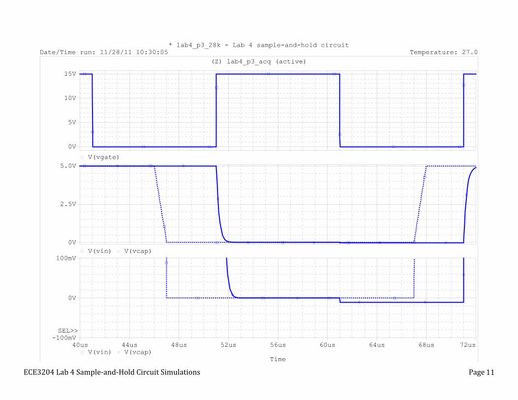
ECE3204 Lab 4 Sample-‐and-‐Hold Circuit Simulations Page 11
Date/Time run: 11/28/11 10:30:05* lab4_p3_28k - Lab 4 sample-and-hold circuit
Temperature: 27.0
Date: November 28, 2011 Page 1 Time: 10:37:58
(Z) lab4_p3_acq (active)
Time
40us 44us 48us 52us 56us 60us 64us 68us 72usV(vin) V(vcap)
-100mV
0V
100mV
SEL>>
V(vin) V(vcap)0V
2.5V
5.0VV(vgate)
0V
5V
10V
15V

ECE3204 Lab 4 Sample-‐and-‐Hold Circuit Simulations Page 12
Date/Time run: 11/28/11 10:30:05* lab4_p3_28k - Lab 4 sample-and-hold circuit
Temperature: 27.0
Date: November 28, 2011 Page 1 Time: 10:39:33
(Z) lab4_p3_acq (active)
Time
20us 24us 28us 32us 36us 40us 44us 48us 52usV(vin) V(vcap)
4.9V
5.0V
5.1V
SEL>>
V(vin) V(vcap)0V
2.5V
5.0VV(vgate)
0V
5V
10V
15V