laboratory experiments
DESCRIPTION
Laboratory Experiments Laboratory Experiments vLaboratory ExperimentsTRANSCRIPT
EE 221 - ANALOG ELECTRONICS LABORATORY EXPERIMENTS
Anh Dinh, Rory Gowen, Chandler Janzen
Department of Electrical and Computer Engineering University of Saskatchewan, Canada
0. Self-taught tutorial - Circuit measurements using Analog Discovery Design kit:
Students construct a circuit on a breadboard then use the Analog Discovery Module® and Waveforms® software to measure and plot various current and voltage nodes on the circuit.
1. Non-ideal operational amplifier and op-amp circuits: In this lab, the students evaluate characteristics of the non-ideal operational amplifiers. Students use a simulation tool (SPICE) to simulate the two most popular configurations op-amp circuits (inverting and non-inverting amplifiers). Students also build, predict the results, and observe the gain and frequency response of the amplifiers.
2. Diode characteristics and diode circuits: At the end of this lab, the students should be able to compare the experimental data to the theoretical curve of the diodes. The students use the Analog Discovery Module® and Waveforms® software to plot the I-V characteristics of the diodes. The students also construct rectifier and filter circuits using diodes and capacitors.
3. BJT I-V characteristics: Students identify the current-control terminal of a three-
terminal active device. The students will use the scanned-load-line methods to obtain the I-V characteristic of the BJTs. The measurement results are to be compared with the I-V curve obtained from the specification posted by the manufacturers.
4. BJT amplifier: In this lab, students design and implement single-stage BJT amplifiers and learn the frequency response of an amplifier.
5. MOSFET I-V characteristics: students discover the voltage-control terminal of the four-terminal MOSFET. The students will construct the circuit and use scanned-load-line method to obtain the MOSFET I-V characteristics. The Analog Discovery Kit is to be used as the main equipment in this experiment. The measurement results are to be compared with the I-V curve obtained from the specifications posted by the manufacturers.
6. FET amplifier: In this lab, students design and implement single-stage FET amplifiers
and explore the frequency response of the real amplifiers. The students will compare the gain and frequency response of the MOSFET amplifier and the BJT amplifier in Lab 4.

2
HEALTH AND SAFETY
Any laboratory environment may contain conditions that are potentially hazardous to a person’s health if not handled appropriately. The electrical engineering laboratories obviously have electrical potentials that may be lethal and must be treated with respect. In addition, there are also mechanical hazards, particularly when dealing with rotating machines, and chemical hazards because of the materials used in various components. Our LEARNING OUTCOME is to educate all laboratory users to be able to handle laboratory materials and situations safely and thereby ensure a safe and healthy experience for all. Watch for posted information in and around the laboratories, and on the class web site.

3
LAB REPORT
Students work in a group of 2, the laboratory is on alternative week. Each student must have a notebook for the labs. The notebook is used for lab preparation, notes, record, and lab reports. The reports must be handed before 5:00pm on the due date into the box labeled to your section. The reports are due on the same date of the following week. The lab book is marked and returned before the next lab.
Marking Scheme
Your grade in the laboratory section is based on two criteria:
Day-to-day lab performance Lab books/notebook keeping
The day-to-day lab performance is based on the lab instructor’s observation of you and
your conduct. This includes your competency at setting experiments up and working the test equipment. It also includes your preparation for the labs, attendance, tardiness, attitude, accuracy, and is also based on your answers, should he/she ask you any questions during the course of the lab. Keep in mind that your behavior influences your grade; act professionally at all times.
Your lab write-ups may be marked with one of the following grades:
Unsatisfactory (repeat) Beginning Developing Satisfactory Advanced
Combinations of any two may also be used. These word grades are translated into number grades by your instructor when compiling your grade for the class. All labs must be performed and a write-up submitted in order to pass the class. If one or more labs have not been performed, then a grade of “INC” (incomplete) will be submitted.
Lab notebooks can be considered to be fulfilling the same functions as logbooks in
industry. Logbooks are used to record the results of all tests performed on systems, subsystems and equipment during the various phases of a project including R&D, design, systems integration, etc. Logbooks are official, permanent documents, and can be used in court to prove ownership of a design!
The following points must be followed when writing up lab reports:
The first page must contain a table of contents. All pages in the notebook must be numbered. Formal structure is not critical; logical order is important. Try to use pen, avoid pencil. Legibility and neatness are important, as is orderly notes.

4
The lab book is standalone. There should be no references to any outside documents. Remember that you may be allowed to bring in your lab books for the final exam. They are your cheat sheets—make sure they’re complete!
Theory and background information must be completed prior to the lab. Cross out unwanted or erroneous material with a single large X. Do not remove
any pages from your lab book. The left-hand page can be used for rough calculations, notes, measurements, etc.
This page is not considered part of the “official” write-up, unless you ask that it be considered.
Do not cut and paste any material from the lab manual into your lab book; only graphs, plots, experimental waveforms, and schematics can. Use glue wherever possible; tape is acceptable, but staples are not!
One lab partner must have the original of any experimental waveform; his/her partner may have a photocopy of that waveform.
Label all diagrams and schematics; include an equipment list. Schematic diagrams and waveforms without explanation are not acceptable. Discussion of results and/or conclusions resulting from each portion of the lab
should be found with that portion. The end of the lab should have a short summary of all conclusions.
The instructors may request you to hand-in your lab books at the end of the term for accreditation purposes.
If in doubt about what to include (and how), remember that it should be clear, concise
and complete.
5
TUTORIAL
This is a self-taught tutorial, go through the tutorial in your own time. If you have any question or need help, contact the support engineers or your instructor.
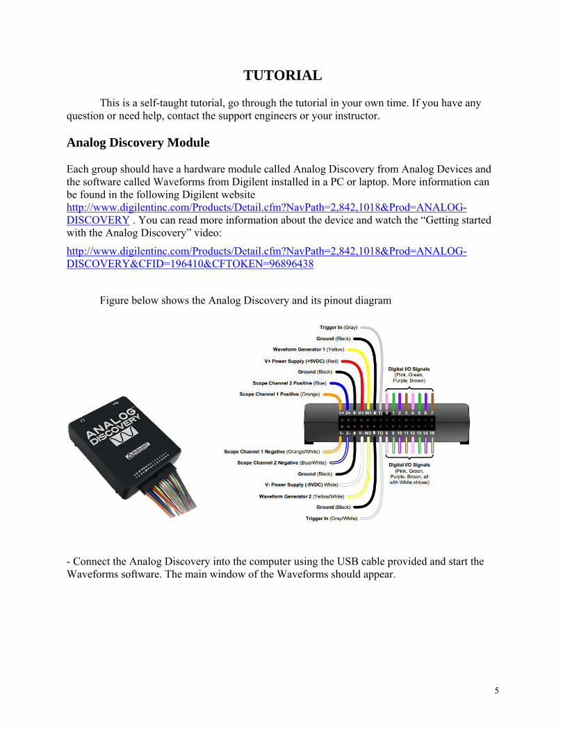
Analog Discovery Module
Each group should have a hardware module called Analog Discovery from Analog Devices and the software called Waveforms from Digilent installed in a PC or laptop. More information can be found in the following Digilent website http://www.digilentinc.com/Products/Detail.cfm?NavPath=2,842,1018&Prod=ANALOG-DISCOVERY . You can read more information about the device and watch the “Getting started with the Analog Discovery” video:
http://www.digilentinc.com/Products/Detail.cfm?NavPath=2,842,1018&Prod=ANALOG-DISCOVERY&CFID=196410&CFTOKEN=96896438
Figure below shows the Analog Discovery and its pinout diagram
- Connect the Analog Discovery into the computer using the USB cable provided and start the Waveforms software. The main window of the Waveforms should appear.

6
- Click on “in”, “out”, and “Voltage” on the “Analog” side of the above window. The following windows will appear (may not be exactly as shown). Size the windows to your best view. These are the 3 main functions of the Analog Discovery and Waveforms.
- The Power Supply (Voltage window) provides +5V (red wire) and -5V (white wire) with respect to ground (black wires).
- The Scope (Oscilloscope 1 window) has 2 channels with differential input. Channel1has 2 wires: positive is orange and negative is orange-white. Channel2 has 2 wires: positive is blue and negative is blue-white. The differential channels allow you to connect the positive or negative side of the channel to anywhere on the circuit (i.e., the scope channels are not grounded unlike those found in a typical oscilloscope). The channel will measure the difference in voltage (in time) between its positive and negative wires.
The “Time” can be changed in “Position” (time) and “Base” (time/division in the horizontal display of the scope).
Note that Channel1 and Channel2 (“C1” and “C2”) have “Offset” (DC level) and “Range” (volt/division on the vertical display of the scopes).
If you need more channels on the scope display, simply click Add Chan. The added channels are derived from C1 and C2. For example, if you want to display the current through a 100 Ω resistor, put C1 across that resistor and Control Add mathematic channel Custom C1/100. This “M1” is the math channel represents the current with the unit of Volt/Ohm=Ampere. By default, the units of the math channel will be Volts. To change the units click the math channel settings button ( ) and select units select the unit from the drop-down menu.
7
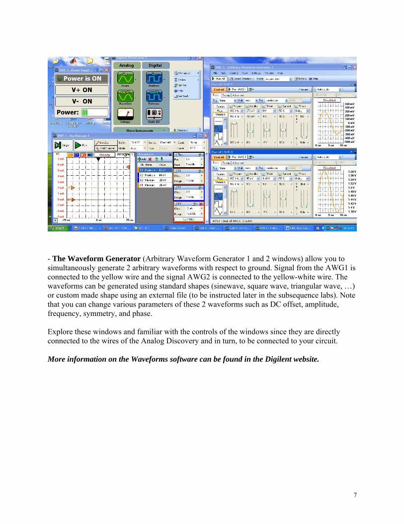
- The Waveform Generator (Arbitrary Waveform Generator 1 and 2 windows) allow you to simultaneously generate 2 arbitrary waveforms with respect to ground. Signal from the AWG1 is connected to the yellow wire and the signal AWG2 is connected to the yellow-white wire. The waveforms can be generated using standard shapes (sinewave, square wave, triangular wave, …) or custom made shape using an external file (to be instructed later in the subsequence labs). Note that you can change various parameters of these 2 waveforms such as DC offset, amplitude, frequency, symmetry, and phase. Explore these windows and familiar with the controls of the windows since they are directly connected to the wires of the Analog Discovery and in turn, to be connected to your circuit. More information on the Waveforms software can be found in the Digilent website.

8
Experiments:
1. Voltage divider circuit.
Construct the circuit below on a breadboard. Connect a sine wave signal (generated by AWG1) with the following parameters (sinewave, 60 Hz frequency, 2.5V amplitude, 2.5V offset, 50% symmetry, 0 degree phase). Perform the followings: - Display C1, C2, M1 (current through R1) at least 4-5 cycles on the oscilloscope window. Note that the alternating current signals (ac) run on top of the DC signal (offset).
- Calculate rms values of VR1, VR2, IR1. Note that the ac rms is: 2
peakRMS
VV
- Observe what happen to the waveforms when you change the signal offset to 3.5V, 1.5V, 0V, and -2.5V.
- Stop AWG1.
The breadboard Note: You may have to adjust the “trigger level” on the scope to stabilize the waveform on the display. The trigger level causes a periodic waveform that crosses the trigger voltage level to snap to the crossing point making the waveform appear stationary in time. To adjust the trigger level select the trigger source ( ) from the drop-down list. After selecting the trigger source a triangle will appear on the right side of the scope window ( ), left click and drag the triangle to set the trigger voltage level. Observe what happens as you adjust the trigger level to cross a waveform.
R1=100Ω
R2=470Ω
AWG1
+ CH2 -+
CH1 -
Ground
Connected horizontally
Connected horizontally
Connected vertically
Voltage divider circuit

9
Example of the scope display. Note: Math Channel M1 displays the current (I=V/R)
2. LED circuit:
Using the above circuit, insert a light emitting diode (LED) between R2 and Ground (make sure the flat side of the LED connected to Ground). Change AWG1 into a standard flat line (DC only). Adjust the DC level from 0-5V and observe at which voltage of AWG1 you can see the LED emitting light. Now change AWG1 to sinewave at an amplitude such that you have an excess at most 1V above the offset you obtain above. Adjust the frequency of the waveform to have a comfortable flashing rate of the LED to be observed (for example 2 flashes per second). Display the voltage waveform across the LED and its current. Change the waveshape to triangular and squarewave (in the AWG1 generator) to observe the LED operation. Stop AWG1.
10
3. RC circuit: Now replace the LED by a 10uF capacitor. Make sure the negative leg of the capacitor is connected to ground if this is a polarized capacitor. Change AWG1 into squarewave of 0 to 5V with a frequency of 10Hz. Display 1 cycle of the waveforms of AWG1 and the voltage across the capacitor. Find the time when the voltage of the capacitor reaching around 63% of its maximum voltage from its minimum voltage. What is the difference of this time to the product of total resistance and capacitance? What is this time called? Note: A polarized capacitor will either have a “+”, “-” or band indicating the positive or negative sides of the capacitor. If you are unsure about whether or not your capacitor is polarized, please ask your instructor, support engineers or teaching assistants for help.
11
LAB 1: NON-IDEAL OPERATIONAL AMPLIFIER AND OP-AMP CIRCUITS
LEARNING OUTCOMES
In this lab, the students evaluate characteristics of the non-ideal operational amplifiers. Students use a simulation tool (SPICE) to simulate the two most popular configurations op-amp circuits (inverting and non-inverting amplifiers). Students also build, predict the results, and observe the gain and frequency response of the amplifiers.
MATERIAL AND EQUIPMENT
Material Equipment TL081 op-amp Analog Discovery module Resistors Waveforms software Photo diode, PNZ334 (or PD204-6C)
PRELAB
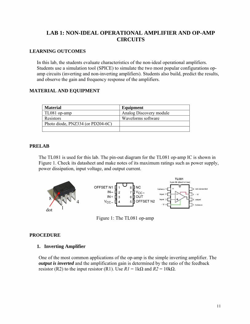
The TL081 is used for this lab. The pin-out diagram for the TL081 op-amp IC is shown in Figure 1. Check its datasheet and make notes of its maximum ratings such as power supply, power dissipation, input voltage, and output current.
Figure 1: The TL081 op-amp
PROCEDURE
1. Inverting Amplifier One of the most common applications of the op-amp is the simple inverting amplifier. The output is inverted and the amplification gain is determined by the ratio of the feedback resistor (R2) to the input resistor (R1). Use R1 = 1kΩ and R2 = 10kΩ.
8 4
1 dot

12
Figure 2: Inverting Amplifier (node numbers in circle correspond to the pin of the TL081 op-amp)
- Simulate the inverting amplifier using ideal op-amp: follow the demonstration by the
instructor of how to simulate the circuit using the Simulation Program with Integrated Circuit Emphasis (SPICE). A sample of a circuit file (inverting.cir) for Figure 2 to be used in the simulation is as follow:
Inverting Amplifier Configuration ** Circuit description ** * opamp circuit .subckt ideal_opamp 1 2 3 Eopamp 1 0 2 3 1e6 .ends ideal_opamp ** Inverting amplifier Vi 1 0 DC 0 AC 0.5V R1 1 2 1k R2 2 6 10k C2 2 6 0.5nF R3 6 0 1k X_A1 6 0 2 ideal_opamp ** Capacitor C2 is put in parallel with resistor R2 to observe frequency response of the amplifier** *Analysis .AC LIN 100 1Hz 100KHz .PLOT AC VdB(6) Vp(6) .probe .end
Simulate the circuit and save the plot of the response (output voltage at different frequencies) of the circuit as the sample below.
R3
1KΩ
vo vin
(AWG1, sinewave,
1KHz, 100mV, 0V,
50%, 0)
R1 1KΩ
_ + ~
43
62
7
+5V
-5V
TL081+ C1 _
+ C2 _
R2 10KΩ
1
C2 0.5nF

13
- Neatly construct the inverting amplifier circuit shown in Figure 2 on a breadboard. See a neatly construct of a circuit breadboard shown in Figure 3 below. Power the op-amp by connecting the power supply of the Analog Discovery (+-5V, red and white wires) to the circuit. Properly ground the circuits using the Analog Discovery ground (the black wire).
Figure 3: Sample of wiring circuits on the breadboard.
- Use the waveform generator of the Analog Discovery (AWG1) to generate the sinewave input signal and connected the signal into the amplifier. Use the scope channels (C1- orange wire and C2 – blue wire) of the Analog Discovery to measure input and output of the amplifier (Vin and Vo). Note: C1 and C2 are the scope channels, not the capacitors.
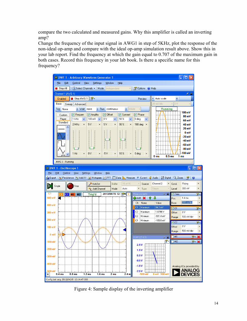
- Turn on the power supply, run AWG1 and the oscilloscope. The samples of the AWG1 and the scope display are shown in Figure 4.
Derive the gain formula Av= -R2/R1 and experimentally verify the gain for a 1 kHz sine wave. For your lab report, show the input and output waveforms. Give your derivation and
14
compare the two calculated and measured gains. Why this amplifier is called an inverting amp? Change the frequency of the input signal in AWG1 in step of 5KHz, plot the response of the non-ideal op-amp and compare with the ideal op-amp simulation result above. Show this in your lab report. Find the frequency at which the gain equal to 0.707 of the maximum gain in both cases. Record this frequency in your lab book. Is there a specific name for this frequency?
Figure 4: Sample display of the inverting amplifier
15
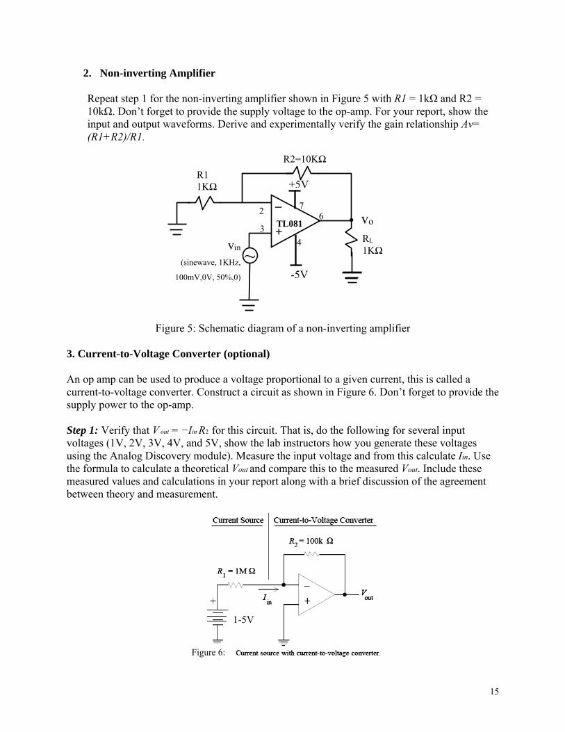
2. Non-inverting Amplifier Repeat step 1 for the non-inverting amplifier shown in Figure 5 with R1 = 1kΩ and R2 = 10kΩ. Don’t forget to provide the supply voltage to the op-amp. For your report, show the input and output waveforms. Derive and experimentally verify the gain relationship Av= (R1+R2)/R1.
Figure 5: Schematic diagram of a non-inverting amplifier 3. Current-to-Voltage Converter (optional)
An op amp can be used to produce a voltage proportional to a given current, this is called a current-to-voltage converter. Construct a circuit as shown in Figure 6. Don’t forget to provide the supply power to the op-amp. Step 1: Verify that V out = −Iin R2 for this circuit. That is, do the following for several input voltages (1V, 2V, 3V, 4V, and 5V, show the lab instructors how you generate these voltages using the Analog Discovery module). Measure the input voltage and from this calculate Iin. Use the formula to calculate a theoretical Vout and compare this to the measured Vout. Include these measured values and calculations in your report along with a brief discussion of the agreement between theory and measurement.
1-5V
RL
1KΩ
R2=10KΩ
vo
vin
(sinewave, 1KHz,
100mV,0V, 50%,0)
R1 1KΩ
_ +
~4
36
27
+5V
-5V
TL081
Figure 6: h di

16
Step 2: Now replace the current source with a photodiode as shown in Figure 7. Notice that the photodiode is reverse-bias connected. The current of the diode is proportional to the illuminance of the light. Look at Vout with the oscilloscope. Find the currents Iin with the light in the room and another light source provided in the lab for your report. The experiment can be done by replacing the photodiode with a Flexiforce sensor connected in series with a 2KΩ resistor. The resistance of the sensor is inversely proportional to the force applied to the sensor (by squeezing on the sensing portion of the sensor). The current is proportional to the force hence the output voltage relates to the force.
Flexiforce to replace the photodiode
5V 5V
Figure 7: Photodiode with current-to-voltage converter

17
LAB 3: DIODE CHARACTERISTICS AND DIODE CIRCUITS
LEARNING OUTCOME
At the end of this lab, the students should be able to compare the experimental data to the theoretical curve of the diodes. The students use the Analog Discovery module to plot the I-V characteristics of the diodes. The students also construct rectifier and filter circuits using diodes and capacitors.
MATERIAL AND EQUIPMENT
Material Equipment
1N4005 (rectifier diode) Analog Discovery module
1N4733 (zener diode) Waveforms software
1N4148 (signal diode)
Assorted resistors (100ohms, 10Kohms), capacitors
PRE LAB
Look up the characteristics of the 1N4005 diode by making a web search. The specifications for different kinds of diode vary. Copy the maximum/minimum rates and the electrical characteristics of the specifications for the diode to your lab report as part of your lab report. Understand the terms used in the specifications.
THEORY
The simplest and most fundamental nonlinear circuit element is the diode. The diode is a device formed from a junction of n-type and p-type semiconductor material, shown in Figure 1(a). The lead connected to the p-type material is called the anode and the lead connected to the n-type material is the cathode, shown in Figure 1(b). In general, the cathode of a diode is marked by a solid line on the diode package, shown in Figure 1(c).
Figure 1: (a) PN-junction model, (b) schematic symbol, and (c) physical part for a diode.
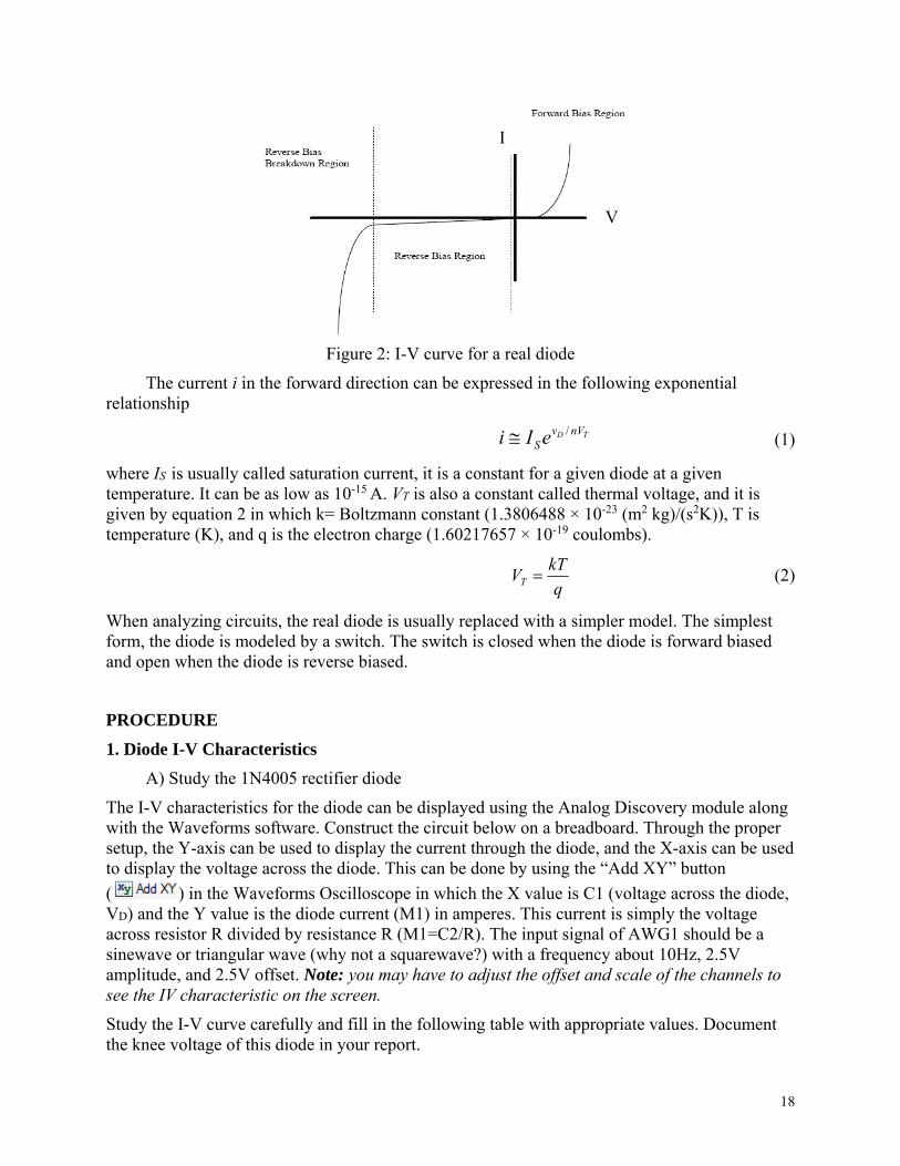
One of the primary functions of the diode is the rectification. When it is forward biased (the higher potential is connected to the anode lead), it will pass current. When it is reverse biased (the higher potential is connected to the cathode lead), the current is blocked. The characteristic curves of an ideal diode and a real diode are seen in Figure 2.
18
Figure 2: I-V curve for a real diode
The current i in the forward direction can be expressed in the following exponential relationship
TD nVvSeIi / (1)
where IS is usually called saturation current, it is a constant for a given diode at a given temperature. It can be as low as 10-15
A. VT is also a constant called thermal voltage, and it is given by equation 2 in which k= Boltzmann constant (1.3806488 × 10⁻²³ (m2 kg)/(s2K)), T is temperature (K), and q is the electron charge (1.60217657 × 10⁻¹⁹ coulombs).
q
kTVT (2)
When analyzing circuits, the real diode is usually replaced with a simpler model. The simplest form, the diode is modeled by a switch. The switch is closed when the diode is forward biased and open when the diode is reverse biased.
PROCEDURE
1. Diode I-V Characteristics
A) Study the 1N4005 rectifier diode
The I-V characteristics for the diode can be displayed using the Analog Discovery module along with the Waveforms software. Construct the circuit below on a breadboard. Through the proper setup, the Y-axis can be used to display the current through the diode, and the X-axis can be used to display the voltage across the diode. This can be done by using the “Add XY” button
( ) in the Waveforms Oscilloscope in which the X value is C1 (voltage across the diode, VD) and the Y value is the diode current (M1) in amperes. This current is simply the voltage across resistor R divided by resistance R (M1=C2/R). The input signal of AWG1 should be a sinewave or triangular wave (why not a squarewave?) with a frequency about 10Hz, 2.5V amplitude, and 2.5V offset. Note: you may have to adjust the offset and scale of the channels to see the IV characteristic on the screen.
Study the I-V curve carefully and fill in the following table with appropriate values. Document the knee voltage of this diode in your report.
I
V

19
Points Diode Voltage (V) Diode Current (A) Characteristic
1 Off
2 Off
3 Just turning on
4 0.6
5 0.65
6
Figure 3: Diode IV characteristic circuit
B) Repeat the same procedure for 1N4148.
Points Diode Voltage (V) Diode Current (A) Characteristic
1 Off
2 Off
3 Just turning on
4 0.6
5 0.65
6
C) Explain the differences of the data between 1N4148 and 1N4005 if applicable and document it in your final report. Hints: silicon diodes can be classified as signal diodes and rectifier diodes.
2. Half-Wave Rectifier Properties
The half-wave rectifying properties of the diode can be displayed using the circuit shown in Figure 4. Build the circuit on a breadboard. Use R = 1k ohms and a 1N4005 diode. Set the signal generator AWG1 so that it can provide an output of:
• Sinusoidal signal
• Amplitude: 5V p-p with an offset of 0V
• Frequency: 60Hz
A. Display the waveforms for the input and output voltages (Vin and Vout) using the oscilloscope. Copy the waveforms in your lab report, and label the peak voltages of the waveforms. Explain the amplitude and time differences between Vin and Vout.
R=560Ω
AWG1 + CH2 -
+ CH1 -
Ground

20
B. Add a 10 μF capacitor in parallel with resistor R, the other parts remain the same. Please notice the + and - signs on the capacitor if you use a polarized capacitor, make sure the polarization is correct, otherwise it may blow up. Display the input and output voltage waveforms and copy into your report. Label the ripple voltage (peak-peak) in the waveform.
In your report, hand in the labeled waveforms obtained in (A) and (B). In addition, calculate the ripple voltage using information from the text book and compare it to the experimental result.
Figure 4: Schematic of the half-wave rectifier diode circuit.
Optional: Build a full-wave rectifier using 2 diodes and the Analog Discovery module.
3. Zener Diode Characteristics
The zener diode has the unique property of maintaining a desired reverse biased voltage. This makes it useful in voltage regulation. In this exercise, you are to tabulate the regulating properties of the Zener diode. Connect the circuit as shown in Figure 5, use 220 ohms resistor and 1N4733 zener diode.
Figure 5: Zener diode voltage regulation
Measure the zener diode properties by varying the input voltage and measuring the voltage across the diode and the current through the diode. Fill in the following table when you measure the voltage and current. Show the lab instructor how you connect the circuit to have the input voltage up to 7V from the Analog Discovery module.
Id
1N4733 Vin 220 Ohms
21
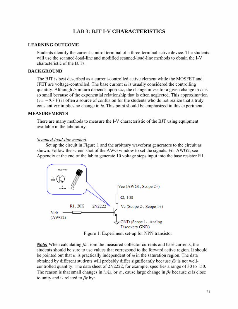
LAB 3: BJT I-V CHARACTERISTICS
LEARNING OUTCOME
Students identify the current-control terminal of a three-terminal active device. The students will use the scanned-load-line and modified scanned-load-line methods to obtain the I-V characteristic of the BJTs.
BACKGROUND
The BJT is best described as a current-controlled active element while the MOSFET and JFET are voltage-controlled. The base current iB is usually considered the controlling quantity. Although iB in turn depends upon vBE, the change in vBE for a given change in iB is so small because of the exponential relationship that is often neglected. This approximation (vBE =0.7 V) is often a source of confusion for the students who do not realize that a truly constant vBE implies no change in iB. This point should be emphasized in this experiment.
MEASUREMENTS
There are many methods to measure the I-V characteristic of the BJT using equipment available in the laboratory.
Scanned-load-line method:
Set up the circuit in Figure 1 and the arbitrary waveform generators to the circuit as shown. Follow the screen shot of the AWG window to set the signals. For AWG2, see Appendix at the end of the lab to generate 10 voltage steps input into the base resistor R1.
Figure 1: Experiment set-up for NPN transistor
Note: When calculating F from the measured collector currents and base currents, the students should be sure to use values that correspond to the forward active region. It should be pointed out that iC is practically independent of iB in the saturation region. The data obtained by different students will probably differ significantly because F is not well-controlled quantity. The data sheet of 2N2222, for example, specifies a range of 30 to 150. The reason is that small changes in iC/iE, or , cause large change in F because is close to unity and is related to F by:

22
1F (1)
where F varies from 30 to 150, changes only from 0.967 to 0.993. The saturation voltage VCEsat is subject to the same kind of misinterpretation by the students is Vf. Its value is often quoted as 0.2 or 0.3 V, but it is actually a monotonically increasing function of iB.
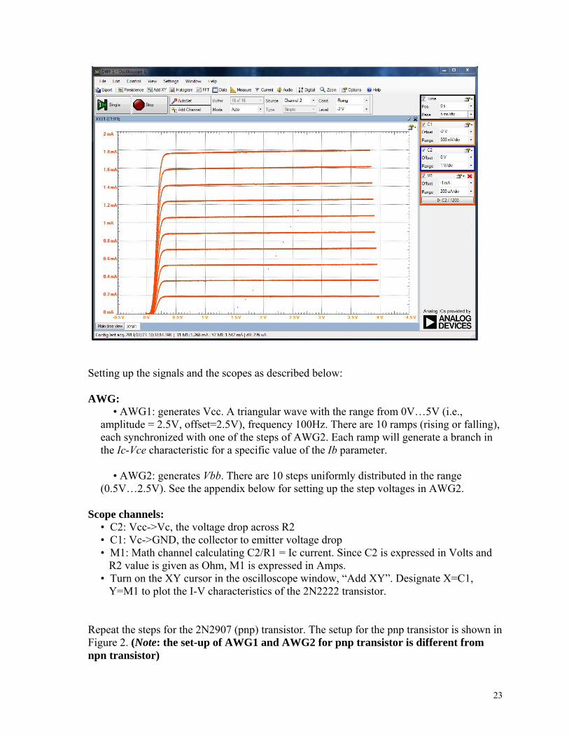
Generate 2 waveforms similar to those shown in the above example (refer to the appendix for further setup instructions). Click on the XY cursor in the oscilloscope window to turn on the XY plot to show the I-V characteristics of the 2N2222 transistor similar to the sample below. The X axis should be the voltage across collector and emitter (VCE in volts) and the Y axis should be the collector current (IC in mili-ampere). The current is to be calculated by using the math channel M1 after clicking on the “Add channel” cursor. Change the waveform into sinewave and squarewave to observe (and explain) if there any change in the I-V characteristic display.
23
Setting up the signals and the scopes as described below: AWG:
• AWG1: generates Vcc. A triangular wave with the range from 0V…5V (i.e., amplitude = 2.5V, offset=2.5V), frequency 100Hz. There are 10 ramps (rising or falling), each synchronized with one of the steps of AWG2. Each ramp will generate a branch in the Ic-Vce characteristic for a specific value of the Ib parameter.
• AWG2: generates Vbb. There are 10 steps uniformly distributed in the range
(0.5V…2.5V). See the appendix below for setting up the step voltages in AWG2. Scope channels:
• C2: Vcc->Vc, the voltage drop across R2 • C1: Vc->GND, the collector to emitter voltage drop • M1: Math channel calculating C2/R1 = Ic current. Since C2 is expressed in Volts and
R2 value is given as Ohm, M1 is expressed in Amps. • Turn on the XY cursor in the oscilloscope window, “Add XY”. Designate X=C1,
Y=M1 to plot the I-V characteristics of the 2N2222 transistor. Repeat the steps for the 2N2907 (pnp) transistor. The setup for the pnp transistor is shown in Figure 2. (Note: the set-up of AWG1 and AWG2 for pnp transistor is different from npn transistor)
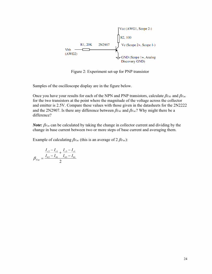
24
Figure 2: Experiment set-up for PNP transistor
Samples of the oscilloscope display are in the figure below. Once you have your results for each of the NPN and PNP transistors, calculate Fdc and Fac for the two transistors at the point where the magnitude of the voltage across the collector and emitter is 2.5V. Compare these values with those given in the datasheets for the 2N2222 and the 2N2907. Is there any difference between Fdc and Fac? Why might there be a difference? Note: Fac can be calculated by taking the change in collector current and dividing by the change in base current between two or more steps of base current and averaging them. Example of calculating Fac (this is an average of 2 Fac):
213
13
12
12
bb
cc
bb
cc
Fac
II
II
II
II

25
Appendix: SOME DETAILED INFORMATION IN THE EXPERIMENT: Some hints for experiment building:
1- To generate the “stairs” signal of AWG2, start from an Excel file with 1,2,3,4,5,… 10 in 10 rows. Save that in .csv or .txt format (source file) and then import in the AWG (set Channel 2 to “Custom”, click “File” and select the source file).
a- When imported, the data in the source file is scaled both in time and range domain:
- Each value in the source file is replicated as needed, such a way to fulfill the AWG buffer.
- Each value in the source file is scaled to (-100%...+100%) range. The smallest value results in -100%, the biggest one results in +100% and all other data is linearly interpolated.
b- After importing the file, the amplitude, frequency and offset can be set to fit the needed signal specs. Frequency is here understood as the “buffer iteration frequency”; 10Hz means that the whole stair sequence takes 100mS (10ms/step).
2- To generate the “triangle” signal of AWG1, set the phase offset to 90 degrees (we are
trying to line up the start/stop of a rising or falling ramp with the start and stop of an AWG2 voltage step). This way the project uses the rising and falling ramp for a value of Vbb. If the frequency is set to 50Hz this results in 10ms for each rising and falling ramp (i.e. one entire rising or falling ramp per voltage step of AWG2).
3- Scope and other things:
- To hide the “connections” between branches of the XY view of the characteristic family, the XY view of the Oscilloscope is set (by default) to show only points. You can change to the curve mode by clicking in the Oscilloscope window: Settings Options Display-XY dots = False.
- To keep absolute synchronism between AWG1 and AWG2, set “Auto sync” mode
( ), With AWG2 as Master. Also set “Run: Infinite” (should be set by default ), for AWG2 channel. Then click the “Run All”
button ( ) to start both waveform outputs. “Auto sync” mode re-synchronizes channels at the largest period of the two channels (100ms from AWG2, in this case)
26
LAB 4: BJT AMPLIFIER LEARNING OUTCOMES:
In this lab, students design and implement single-stage BJT amplifiers and observe amplitude and frequency responses. Breadboard and the Analog Discovery module are to be used. The students will use various tools and functions from the Waveform software to perform measurement and plotting the amplifier response.
MATERIAL AND EQUIPMENT:
Material Equipment 2N2222 npn BJT transistor Breadboard Capacitors Multimeter Resistors Analog Discovery 2N2907 pnp BJT transistor Digilent Waveform software
PRE-LAB
Look at this handout and be familiar with the CE amplifier described in the text book. You need to know how to calculate the DC voltage, current and small-signal gain. Design an amplifier with a voltage gain of -4, a collector current of 5 mA, bias the collector voltage to provide a maximum output voltage swing (i.e., collector voltage Vc equals to ½ of Vcc). The bias resistance R1 and R2 should be in the range of 1K to 20K (why?). Use a Vcc of +5 V from the power supply of the Analog Discovery module.
PROCEDURES 1. NPN transistor characteristics
Obtain 2N2222 Si npn from the lab instructor or from the teaching assistant. Measure its
βDC at VCE =2.5V if you don’t have the current gain of this transistor from the previous lab.
You need to include the transistor characteristics in your lab report. Label βDC on the curves.
The normal βDC of 2N2222 is between 100-200. Also use the information in Lab 3 BJT I-V
characteristics. 2. Common Emitter (CE) amplifier
Design and construct the circuit shown in Figure 1. You can use 1 uF for capacitor CB and 4.7 uF for the capacitor CC.
A. Measure the DC currents and voltages: IB, IC, IE, VC, VB, VE. Remember to measure one
at a time with NO input AC signal. In your report, make a table and list the results from

27
your experiment and hand calculations. In your hand calculation, use β determined from
your I-V curve. Assume VBE = 0.7V. B. At this time, DO NOT connect the load resistor RL . Generate an input signal from
AWG1 (100 mVpp, 1 KHz) and send the signal to the input of the amplifier. Observe the input and output voltage waveforms using two probes of the oscilloscope (Channel 1 and Channel 2). First observe the waveforms of the input signals that are before and after CB. Note that how DC voltage at the base is preserved by using the coupling capacitor CB. Then observe the waveforms of signals Vc and Vo that are before and after coupling capacitor CC. The waveform at Vc has both ac and DC components and waveform at Vo is a pure ac signal because of the coupling capacitor CC blocking all the DC component in the signal. Capture the waveforms at Vi, VB, Vc and Vo and copy them to your lab report. Find the voltage gain from the waveforms (Vo/Vi).
Figure 1: CE amplifier
C. Perform hand calculations for the output voltage and voltage gain. List the results from your experiment and hand calculation in a table in your lab report.
D. Connect the load resistor RL = 1K to the amplifier. Read the output voltage from the oscilloscope and find the voltage gain.
E. Connect a polarized capacitor CE =22 uF to the circuit as shown in Figure 1 so that it is in parallel with RE . At this time, the emitter is ac shorted to ground. Observe the output waveform at Vc and Vo and copy it to your lab report. Explain why the waveforms are distorted. Once you have finished this step, recover the circuit connection according to Figure 1 by removing CE and RL.
F. At the last step, you need to adjust the frequency of the input signal from the signal generator. First you need to reduce the frequency (below 1kHz) and observe the voltage gain. The gain will reduce after a certain frequency. Find the low frequency, fL, when the voltage gain is decreased to 70% (half-power). Then you need to increase the frequency (about 1kHz) and find the high frequency, fH, when voltage gain is reduced to 70%. The amplifier bandwidth is defined as fH-fL. Document the frequencies and bandwidth in your report. Read Appendix 1 and Appendix 2 in Lab5 FET Amplifier (page 37).
2N2222
+5V
To Channel 2 of the oscilloscope RC
R2 RE
CC
CB
CE
To Channel 1 of the oscilloscope
~AWG1
R1 VC
VO VB
Vi RL
28
G. Optional: Use “Sweep” function in the Arbitrary Waveform Generator to sweep the frequency of the input signal and observe the response of the amplifier. Describe the response of the amplifier.
H. Optional: Repeat the steps using 2N2907 (pnp) transistor. Comment on the differences between npn and pnp amplifiers.
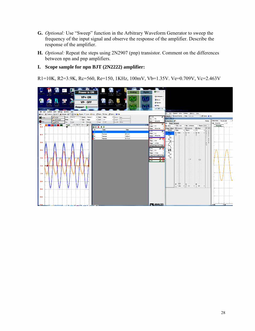
I. Scope sample for npn BJT (2N2222) amplifier: R1=10K, R2=3.9K, Rc=560, Re=150, 1KHz, 100mV, Vb=1.35V. Ve=0.709V, Vc=2.463V
29
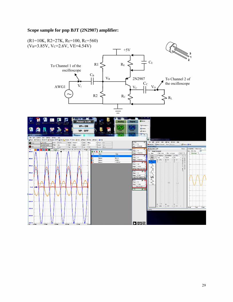
Scope sample for pnp BJT (2N2907) amplifier: (R1=10K, R2=27K, RE=100, RC=560) (VB=3.85V, VC=2.6V, VE=4.54V)
2N2907
+5V
To Channel 2 of the oscilloscope
RE
R2 RC
CC
CB
CE To Channel 1 of the
oscilloscope
~AWG1
R1
VC VO
VB
Vi
RL
30
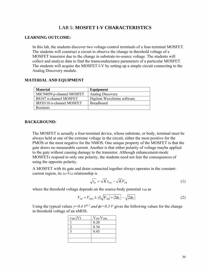
LAB 5: MOSFET I-V CHARACTERISTICS LEARNING OUTCOME:
In this lab, the students discover two voltage-control terminals of a four-terminal MOSFET. The students will construct a circuit to observe the change in threshold voltage of a MOSFET transistor due to the change in substrate-to-source voltage. The students will collect and analyze data to find the transconductance parameters of a particular MOSFET. The students will acquire the MOSFET I-V by setting up a simple circuit connecting to the Analog Discovery module.
MATERIAL AND EQUIPMENT
Material Equipment MIC94050 p-channel MOSFET Analog Discovery BS107 n-channel MOSFET Digilent Waveforms software IRFD110 n-channel MOSFET Breadboard Resistors
BACKGROUND:
The MOSFET is actually a four-terminal device, whose substrate, or body, terminal must be always held at one of the extreme voltage in the circuit, either the most positive for the PMOS or the most negative for the NMOS. One unique property of the MOSFET is that the gate draws no measurable current. Another is that either polarity of voltage maybe applied to the gate without causing damage to the transistor. Although enhancement-mode MOSFETs respond to only one polarity, the students need not fear the consequences of using the opposite polarity.
A MOSFET with its gate and drain connected together always operates in the constant-current region, its iD-VGS relationship is
TRGSD VKvKi (1)
where the threshold voltage depends on the source-body potential vSB as
FFSBTRTR VVV 22[0 (2)
Using the typical values γ=0.4 V0.5 and F=0.3 V gives the following values for the change in threshold voltage of an nMOS.
vSB (V) VTR-VTR0 1 0.20 2 0.34 3 0.45

31
OBSERVE THE CHANGE IN THRESHOLD VOLTAGE DUE TO SUBSTRATE-TO-SOURCE VOLTAGE (VSB):
Set up the circuit as shown in Figure 1 below. Use the MIC94050 p-channel MOSFET, this transistor has 4 terminals in which the substrate is marked on the mounting PCB. Connect the circuit to the Analog Discovery module, pay attention to the polarities of the scope Channels 1 and 2. Start Digilent Waveforms software and WaveGen (out). Set-up the 2 output waveforms AWG1 and AWG2 using the parameters provided in Table 1. Consult the detailed information at the end of this document of how to set-up the desired waveforms in the Analog Discovery module. Start the Scope (in) and set-up the channels (C1, C2, and Math Channel M1) as shown in the example waveforms in Figure 3. Add XY in the Oscilloscope 1 window and select X=C1 and Y=M1. Run two waveforms generated in the WaveGen (Run all). Run the oscilloscope and observe the waveform of the window XY#1. The waveform should be similar to the samples in Figure 3.
Table 1: Initial Waveforms parameters set-up
Waveform Gen. Frequency (Hz) Amplitude Offset
AWG1 (sawtooth) 10 2.5V -2.5V
AWG2 (5 steps) 1 1.5V 1.5V
Channel Math Offset Range
C1 -1.1V 100mV/div
C2 -2V 500mV/div
M1 C2/RD -5mA 1mA/div
Time Start 0 Base 200ms/div
Figure 1: Circuit set-up to observe the substrate voltage
The plots of Di vs vGS will look like these in Figure 2. Each curve corresponds to a
different value of vSB. The slope of each curve is K . Extrapolating each curve to iD=0 gives threshold voltage, VTR, for each value of vSB. The curves are not equally spaced
because the change in VTR is proportional to SBV . Measure the voltage vGS, current iD with
the Digilent scope for different values of vSB. Plot as shown in Figure 2.
Obtain a printout of the XY waveform, label the values of VSB on each curve. (The waveform can be exported as data and can be saved into your computer). Use your favorite software to plot the linear region of the curves. The slope of each curve is K . Find K in mA/V2. Using your measurements find VTR0 (i.e., threshold voltage when VSB=0V).
RD,560
G
D
SSubstrate
To AWG2
To AWG1
+ Channel 2 _
+ Channel 1 _
MIC94050

32
Setup of step voltage on AWG:
- Digilent waveforms 1 Analog Out Wave Gen Open new.
- DWF1 – Arbitrary Waveform Generator 1 will appear.
- Generator 1 Select Channels Channel 1 (AWG1) Chanel 2 (AWG2)
- Selecting Ch. 2 AWG2 Generator opens the second Generator. Run All, Stop All will control both Generators.
- Generator AWG2 Custom File Five Setps.csv open open. This file was created in Excel (1 column with 5 rows of values: 1, 2, 3, 4, 5), the file can be saved as csv file or text file.
- Adjust Gen. Frequency, Amplitude and Offset.
Use Figure 1: Determine VTR0
- Connect substrate to source (ground the substrate to make VSB=0V).
- Disconnect AWG2.
- From XY Plot determine VTR0.
Figure 2: Effect of bulk (substrate) voltage on the drain current
VGS
Increasing vSB
Di

33
Note: This figure is only an example of the waveforms, your settings may be slightly different!
34
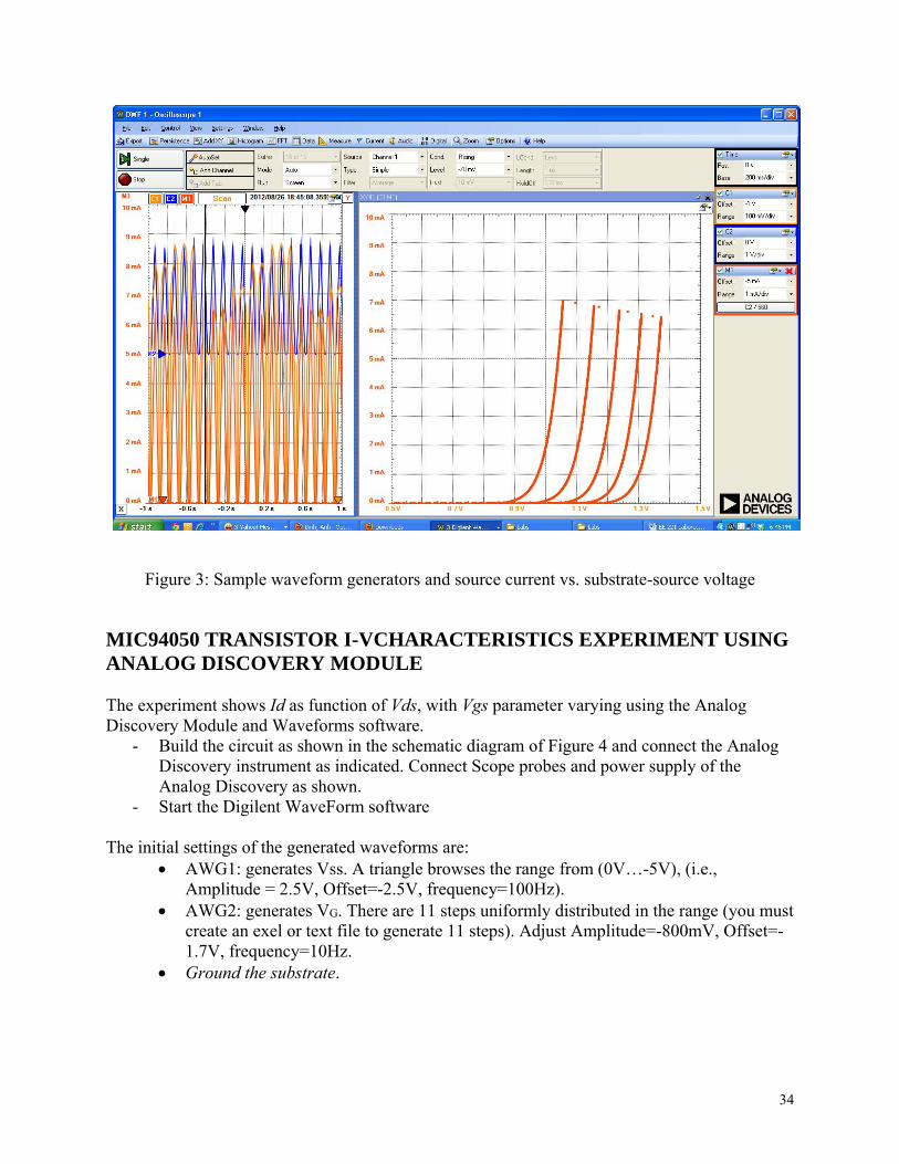
Figure 3: Sample waveform generators and source current vs. substrate-source voltage
MIC94050 TRANSISTOR I-VCHARACTERISTICS EXPERIMENT USING ANALOG DISCOVERY MODULE The experiment shows Id as function of Vds, with Vgs parameter varying using the Analog Discovery Module and Waveforms software.
- Build the circuit as shown in the schematic diagram of Figure 4 and connect the Analog Discovery instrument as indicated. Connect Scope probes and power supply of the Analog Discovery as shown.
- Start the Digilent WaveForm software The initial settings of the generated waveforms are:
AWG1: generates Vss. A triangle browses the range from (0V…-5V), (i.e., Amplitude = 2.5V, Offset=-2.5V, frequency=100Hz).
AWG2: generates VG. There are 11 steps uniformly distributed in the range (you must create an exel or text file to generate 11 steps). Adjust Amplitude=-800mV, Offset=-1.7V, frequency=10Hz.
Ground the substrate.

35
Figure 4: Schematic diagram to obtain I-V characteristics of the p-channel MOSFET
Scope channels: C2: the voltage drop across R1 C1: the source to drain voltage drop M1: Math channel calculating C2/R1 = Id current. Since C2 is expressed in Volts and R1
value is given as Ohm, M1 is expressed in Amps. M2: Math channel calculating (C2/R1)*C1 = Is*Vds = P, the power dissipated by the
transistor. Expressed in Watts. M3: Math channel calculating (C1+C2) = Vss, as generated by AWG1. Main time plot: shows the time diagrams. Only C1, M1 are activated, to keep the image
clean. XY#1: show a representation of the IV characteristics of the transistor in XY plot: vertical =
M1 is the source current Is (or Id, as function of C2) and horizontal = C1 is the source-drain voltage Vds. There are multiple branches of the IV characteristics corresponding to different values of VGS. Get a printout of the waveform, label the values of VGS for each curve.
Measurements: What is the average value of P (transistor dissipated power)? Expressed in Watts. (Hint: P = M2)
Additional Measurements and Questions: Change Vsb (in steps of 500mV) by applying an external voltage to the substrate instead of
connected to GND. Observe, record, describe, and explain the change in IV characteristic of the transistor due to the change of Vsb.
Can the resistor be connected to +5V instead of GND? If so, re-draw the schematic diagram of the circuit (no need to set-up the circuit).
GND (Scope2-)
MIC94050
VG (AWG2,step, 10Hz, -800mV, 1.7V)
Analog GND Vd (Scope1-, Scope2+) R1
560
AWG1(100Hz, 2.5V,-2.5V), (Scope 1+)

36
Sample of the scope windows of MIC94050 characteristic:
37
Optional observation: In the AWG window, observe the preview for the two generated signals: Vg and Vss. in the oscilloscope Main Time plot, activate M2 to see Vss. Notice the voltage drop at high
currents, as AWG limitation. The triangle signal distortion does not affect the XY representation, except the high current branches are a bit shorten (upper right end). Uncheck M2 to return to the clean image.
in the oscilloscope Main Time plot, C1 shows the source voltage, Vs, while M1 shows the source current, Is.
the XY#1 window shows the Is(Vds) characteristic. Each branch is generated during a single step in the Vgg signal. The direction of browsing Vss (rising or falling) does not matter in the XY representation.
o Quiz: what happens if you change the wave shape of AWG2 from triangle to sinusoid?
the Measurement window shows the transistor dissipated power. This value is computed as average for the displayed time frame.
You can start a scope ZOOM window to see the time domain and XY view corresponding to the Zoom1 rectangle in the main time window. Click and drag the Zoom1 rectangle to see what portion of the time diagram corresponds to each branch in the XY view.
Explore further in amplitude, frequency, offset of AWG1 and AWG2. Change time scale, offset, range, … on C1,C2,M1,M2,M3,M4 as necessary. Report what you have explored and observed with clear explanation the characteristic of a p-MOSFET.
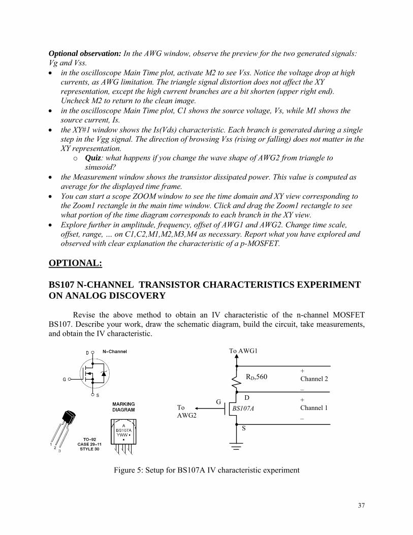
OPTIONAL: BS107 N-CHANNEL TRANSISTOR CHARACTERISTICS EXPERIMENT ON ANALOG DISCOVERY
Revise the above method to obtain an IV characteristic of the n-channel MOSFET BS107. Describe your work, draw the schematic diagram, build the circuit, take measurements, and obtain the IV characteristic.
Figure 5: Setup for BS107A IV characteristic experiment
RD,560
G D
S
To AWG2
To AWG1
+ Channel 2 _
+ Channel 1 _
BS107A

38
Sample scope window of BS107 IV characteristic:
SOME DETAILED INFORMATION IN THE EXPERIMENT: Some hints for experiment building:
- To generate the “stairs” signal of AWG2, start from an Excel file with 1,2,3,4,5 in 5 rows. Save that in .csv or .txt format (source file) and then import in the AWG (set Channel 2 to “Custom”, click “File” and select the source file). When imported, the data in the source file is scaled both in time and range domain:
o Each value in the source file is replicated as needed, such a way to fulfill the AWG buffer (in our case, each of the 100 records generated 20 (or 21) samples, to fill the 2048 samples in the AWG buffer.
o Each value in the source file is scaled to (-100%...+100%) range. The smallest value results in -100%, the biggest one results in +100% and all other data is linearly interpolated.
39
- After importing the file, the amplitude, frequency and offset can be set to fit the needed signal specs. Frequency is here understood as the “buffer iteration frequency”; 10Hz means that the whole stair sequence takes 100mS (10ms/step).
- To generate the “triangle” signal of AWG1, set the initial Phase to 270 degrees. This way the project uses each rising and falling ramp for a value of Vbb. Frequency is set to 50Hz, to result in 10ms for each rising or falling ramp.
- To hide the “connections” between branches of the XY view of the characteristic family, the XY view of the Oscilloscope is set (by default) to show only points. You can change to the curve mode by clicking in the Oscilloscope window: Settings Options Display-XY dots = False.
- - To keep absolute synchronism between AWG1 and AWG2, set “Auto sync” mode
( ), With AWG2 as Master. Also set “Run: Infinite” (should be set by default ), for AWG2 channel. Then click the “Run All”
button ( ) to start both waveform outputs. “Auto sync” mode re-synchronizes channels at the largest period of the two channels (100ms from AWG2, in this case)
40
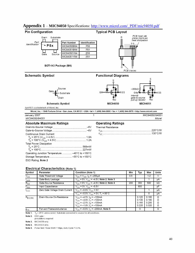
Appendix 1 – MIC94050 Specifications: http://www.micrel.com/_PDF/mic94050.pdf
41
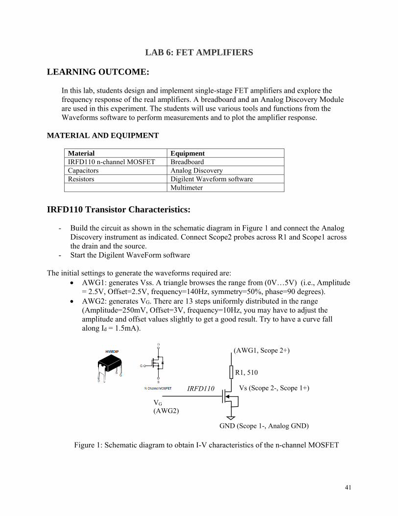
LAB 6: FET AMPLIFIERS LEARNING OUTCOME:
In this lab, students design and implement single-stage FET amplifiers and explore the frequency response of the real amplifiers. A breadboard and an Analog Discovery Module are used in this experiment. The students will use various tools and functions from the Waveforms software to perform measurements and to plot the amplifier response.
MATERIAL AND EQUIPMENT
Material Equipment IRFD110 n-channel MOSFET Breadboard Capacitors Analog Discovery Resistors Digilent Waveform software Multimeter
IRFD110 Transistor Characteristics:
- Build the circuit as shown in the schematic diagram in Figure 1 and connect the Analog Discovery instrument as indicated. Connect Scope2 probes across R1 and Scope1 across the drain and the source.
- Start the Digilent WaveForm software The initial settings to generate the waveforms required are:
AWG1: generates Vss. A triangle browses the range from (0V…5V) (i.e., Amplitude = 2.5V, Offset=2.5V, frequency=140Hz, symmetry=50%, phase=90 degrees).
AWG2: generates VG. There are 13 steps uniformly distributed in the range (Amplitude=250mV, Offset=3V, frequency=10Hz, you may have to adjust the amplitude and offset values slightly to get a good result. Try to have a curve fall along Id = 1.5mA).
Figure 1: Schematic diagram to obtain I-V characteristics of the n-channel MOSFET
GND (Scope 1-, Analog GND)
IRFD110
VG (AWG2)
(AWG1, Scope 2+)
Vs (Scope 2-, Scope 1+)
R1, 510

42
Sample of scope windows:
Figure 2: Scope sample of the n-channel MOSFET I-V characteristic
43
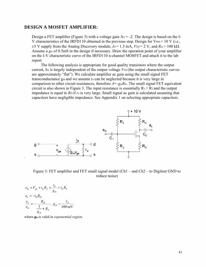
DESIGN A MOSFET AMPLIFIER: Design a FET amplifier (Figure 3) with a voltage gain AV = -2. The design is based on the I-V characteristics of the IRFD110 obtained in the previous step. Design for VDD = 10 V (i.e., 5 V supply from the Analog Discovery module, ID = 1.5 mA, VDS = 2 V, and Rin > 100 kΩ. Assume a gm of 0.5mS in the design if necessary. Draw the operation point of your amplifier on the I-V characteristic curve of the IRFD110 n-channel MOSFET and attach it to the lab report.
The following analysis is appropriate for good quality transistors where the output current, ID, is largely independent of the output voltage VDS (the output characteristic curves are approximately “flat”). We calculate amplifier ac gain using the small signal FET transconductance gm and we assume ro can be neglected because it is very large in comparison to other circuit resistances, therefore A=-gmRD. The small signal FET equivalent circuit is also shown in Figure 3. The input resistance is essentially R1 // R2 and the output impedance is equal to RD if ro is very large. Small signal ac gain is calculated assuming that capacitors have negligible impedance. See Appendix 1 on selecting appropriate capacitors.
.
Figure 3: FET amplifier and FET small signal model (Ch1 – and Ch2 – to Digilent GND to reduce noise)
where gm is valid in exponential region.
44
PROCEDURE:
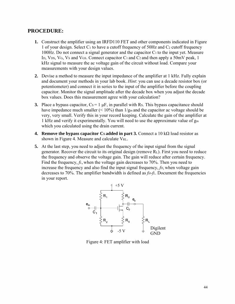
1. Construct the amplifier using an IRFD110 FET and other components indicated in Figure 1 of your design. Select C1 to have a cutoff frequency of 50Hz and C2 cutoff frequency 100Hz. Do not connect a signal generator and the capacitor C1 to the input yet. Measure ID, VDS, VG, VS and VGS. Connect capacitor C1 and C2 and then apply a 50mV peak, 1 kHz signal to measure the ac voltage gain of the circuit without load. Compare your measurements with your design values.
2. Devise a method to measure the input impedance of the amplifier at 1 kHz. Fully explain and document your methods in your lab book. Hint: you can use a decade resistor box (or potentiometer) and connect it in series to the input of the amplifier before the coupling capacitor. Monitor the signal amplitude after the decade box when you adjust the decade box values. Does this measurement agree with your calculation?
3. Place a bypass capacitor, CS = 1 μF, in parallel with RS. This bypass capacitance should have impedance much smaller (< 10%) than 1/gm and the capacitor ac voltage should be very, very small. Verify this in your record keeping. Calculate the gain of the amplifier at 1 kHz and verify it experimentally. You will need to use the approximate value of gm
which you calculated using the drain current.
4. Remove the bypass capacitor CS added in part 3. Connect a 10 kΩ load resistor as shown in Figure 4. Measure and calculate VRL.
5. At the last step, you need to adjust the frequency of the input signal from the signal generator. Recover the circuit to its original design (remove RL). First you need to reduce the frequency and observe the voltage gain. The gain will reduce after certain frequency. Find the frequency, fL, when the voltage gain decreases to 70%. Then you need to increase the frequency and also find the input signal frequency, fH, when voltage gain decreases to 70%. The amplifier bandwidth is defined as fH-fL. Document the frequencies in your report.
Figure 4: FET amplifier with load
-5 V
+5 V
Digilent GND
45
APPENDIX 1 – Selecting coupling capacitors: Be careful when choosing your coupling capacitors (C1 and C2). For this experiment, our largest non-polarized capacitors may be used. Polarized capacitors tend to have “higher” capacitance values, usually ≥ 5 μF, and they are always marked with either a + or a – (or both) next to one of their terminals. They may also be marked with a band to indicate the negative end (same convention as a diode). Remember that the potential of the + terminal should be always higher than the – terminal when connected in a circuit. Otherwise, it will induce the leak current between the two terminals and eventually damage the capacitor. In the signal path of a circuit such as C1 and C2, this condition may not be met in all cases since the connected circuits are unknown. Therefore you should avoid polarized capacitors in the signal path. Coupling capacitors must be chosen so that they have a “small” impedance at the frequency of interest compared with the input impedance of the circuit to which they’re connected. This is to ensure that little voltage will be dropped or lost across the capacitor itself—after all, an amplifier is supposed to amplify voltages, not attenuate them. A good rule of thumb is that Zcoupling C should be no more than approximately 10% of the input impedance of the amplifier (for the input coupling capacitor), or the input impedance of whatever circuit the amplifier drives (for the output coupling capacitor). For the FET amplifier you just constructed, the input impedance is supposed to be > 100 kΩ. Therefore the impedance of C1 at the lowest frequency the amplifier is expected to see should be no more than approximately 10 kΩ. If this lowest frequency is expected to be 100 Hz, then C1 > 0.16 μF. For this experiment, select the appropriate coupling capacitors for C1 at lowest frequency of 50 Hz. Similarly, the amplifier drives a load of 1 kΩ (Figure 4). Following the same argument the impedance of C2 at the lowest expected frequency should be no more than approximately 100 Ω. If this lowest frequency is 100 Hz, then C2 > 16 μF. If the largest non-polarized capacitors available are 2 μF, then C2 would have to be made up of eight 2 μF capacitors in parallel. Alternately, a polarized capacitor could be used with appropriate care given to the polarity of the capacitor.
APPENDIX 2 – Frequency response of the FET amplifier: The typical Frequency Response of an amplifier is presented in a form of a graph that shows output amplitude (or, more often, voltage gain) plotted versus log frequency. Typical plot of the voltage gain is shown in Figure 5. The gain is null at zero frequency, then rises as frequency increases, level off for further increases in frequency, and then begins to drop again at high frequencies. The frequency response of an amplifier can be divided into three frequency regions.

46
Figure 5: Diagram of voltage gain versus frequency for an amplifier.
The frequency response begins with the lower frequency region designated between 0 Hz and lower cutoff frequency. At lower cutoff frequency, fL ,the gain is equal to 0.707 Amid. Amid is a constant midband gain obtained from the midband frequency region. The third, the upper frequency region covers frequency between upper cutoff frequency and above. Similarly, at upper cutoff frequency, fH, the gain is equal to 0.707 Amid. After the upper cutoff frequency, the gain decreases with frequency increases and dies off eventually.
The Lower Frequency Response:
Since the impedance of coupling capacitors increases as frequency decreases, the voltage gain of a FET amplifier decreases as frequency decreases. At very low frequencies, the capacitive reactance of the coupling capacitors may become large enough to drop some of the input voltage or output voltage. Also, the source-bypass capacitor, the capacitor in parallel with the resistor from source to ground (source-resistor), may become large enough so that it no longer shorts the source-resistor to ground. Approximately, the following equations can be used to determine the lower cutoff frequency of the amplifier, where the voltage gain drops 3 dB from its midband value (=0.707 times the midband Amid): (1) f1 = 1/ ( 2πrinC1 ) where: f1 = lower cutoff frequency due to C1, C1 = input coupling capacitance, rin = input resistance of the amplifier. (2) f2 = 1/ ( 2πrout C2 ) where: f2 = lower cutoff frequency due to C2, C2 = output coupling capacitance, rout = output resistance of the amplifier. Provided that f1 and f2, are not close in value, the actual lower cutoff frequency is approximately equal to the largest of the two.
The Upper Frequency Response: Transistors have inherent shunt capacitances between each pair of terminals. At high frequencies, these capacitances effectively short the ac signal voltage.

47
The design using my available resistors, capacitors:
- R1=220K, R2=300K, C1=C2=100nF, Rd=3.9K, Rs=1.6K - Vdd to Vss=9.96V, Vg=0.712V, Vs=-2.664V, Vd=-0.636V - Input: 100mV-peak, 1KHz, note that polarities of Channel 2 are swapped to have the
same phase with input to calculate amplifier gain. Scope:
- XY (C1:C2) shows the slope which is the gain of the amplifier) - M1: 20* Lg ( ( Max ( C2 , 0.095) ) / ( Max ( C1 , 0.095) ) ) = gain in dB - M2: ( Max ( C2 , 0.095) ) / ( Max ( C1 , 0.095) ) is the gain

48
Appendix 3 – IRFD110 Specifications: http://www.vishay.com/docs/91127/sihfd110.pdf