lari nousiainen - trepo.tuni.fi
TRANSCRIPT


Tampereen teknillinen yliopisto. Julkaisu 1087 Tampere University of Technology. Publication 1087 Lari Nousiainen Issues on Analysis and Design of Single-Phase Grid-Connected Photovoltaic Inverters Thesis for the degree of Doctor of Science in Technology to be presented with due permission for public examination and criticism in Sähkötalo Building, Auditorium S4, at Tampere University of Technology, on the 23rd of November 2012, at 12 noon. Tampereen teknillinen yliopisto - Tampere University of Technology Tampere 2012

ISBN 978-952-15-2933-7 (printed) ISBN 978-952-15-2971-9 (PDF) ISSN 1459-2045
ABSTRACT
This thesis provides a comprehensive study of the problems in single-phase grid-connected
photovoltaic (PV) systems. The main objective is to provide an explicit formulation of
the dynamic properties of the power-electronic-based PV inverter in the frequency do-
main. Such a model is used as the main tool to trace the origins of the observed problems
that cannot be studied with the conventional time-domain analyses. The dynamic model
also provides the tool for deterministic control-system design.
Grid-connected PV inverters have been reported to reduce damping in the grid, excite
harmonic resonances and cause harmonic distortion. These phenomena can lead to in-
stability or production outages and are expected to increase in the future, because the
installed capacity of the grid-connected PV energy is rapidly growing. A PV generator
(PVG) itself is a peculiar source affecting the inverter dynamic behavior. The PVG is
internally a current-source with limited output voltage and power. The nonlinear behav-
ior yields distinguishable operating regions: the constant-current region at the voltages
lower than the maximum-power-point (MPP) voltage and constant-voltage region at the
voltages higher than the MPP voltage. Such a behavior is quite well known but not
really understood to need special attention. Vast majority of the photovoltaic inverters
originate from the voltage-source inverter (VSI) with a capacitor connected at the input
terminal for power-decoupling purposes. It is convenient to assume that the inverter is
supplied by a voltage source and perform the analyses based on the existing modeling
and design teqhniques of the voltage-fed (VF) VSI. However, the input voltage of a PV
inverter must be controlled for MPP-tracking purposes, which implies that the inverter
has to be analyzed as a current-fed (CF) inverter. Such analysis reveals that the CF VSI
has second-order dynamics compared to the first-order dynamics of the VF VSI. The
control dynamics of the CF VSI is also shown to incorporate right-half-plane zero and
pole introducing control-system-design constraints.
This thesis presents the dynamic modeling procedure of PV inverter both at open and
closed loop taking into account the type of the input source. The dynamic behavior
of the PVG is modeled as an operating-point-dependent dynamic resistance, which is
shown to shift the operating point dependent zero and pole in the inverter control dy-
namics between the right and left halves of the complex plane. It is also shown that
the negative-incremental-resistance behavior of the inverter output impedance makes the
inverter prone to instability and the grid to harmonic resonance problems, and that such
a behavior can originate e.g. from the grid synchronization and the cascaded control
scheme. It is important to recognize such a behavior in order to enable reliable large-
scale utilization of the PV energy.
iii

PREFACE
This work was carried out at the Department of Electrical Energy Engineering at Tam-
pere University of Technology (TUT) during the years 2009 - 2012. The research was
funded by TUT and ABB Oy. Grants from Fortum Foundation and Foundation for
Technology Promotion (Tekniikan edistamissaatio) are greatly appreciated.
First of all, I want to express my gratitude to Professor Teuvo Suntio for supevising
my thesis work. His mentoring and guidance have been significant driving forces behind
my academic career. Secondly, the other members of our former research group, M.Sc.
Joonas Puukko, M.Sc. Juha Huusari, M.Sc. Tuomas Messo, M.Sc. Anssi Maki, M.Sc.
Diego Torres Lobera and D.Sc. Jari Leppaaho, deserve special thanks for the inspiring
working atmosphere and discussions in professional matters. It was a pleasure to work
with you all. I also want to thank Professor Pertti Silventoinen and Professor Jorma
Kyyra for pre-examining my thesis and Sirpa Jarvensivu for proofreading it. The whole
Department of Electrical Energy Engineering also deserve a thank you for the great work-
ing environment.
I would also like to thank my parents, my brothers and sisters and my wife Jenna for all
the support I have received from them during my studies and in my life.
Kirkkonummi, October 2012
Lari Nousiainen
iv

CONTENTS
Abstract . . . . . . . . . . . . . . . . . . . . . . . . . . . . . . . . . . . . . . iii
Preface . . . . . . . . . . . . . . . . . . . . . . . . . . . . . . . . . . . . . . . iv
Contents . . . . . . . . . . . . . . . . . . . . . . . . . . . . . . . . . . . . . . v
Symbols and abbreviations . . . . . . . . . . . . . . . . . . . . . . . . . . . xi
1. Introduction . . . . . . . . . . . . . . . . . . . . . . . . . . . . . . . . . . 1
1.1 Photovoltaic energy . . . . . . . . . . . . . . . . . . . . . . . . . . . . . . . 1
1.2 Photovoltaic generator as an input source . . . . . . . . . . . . . . . . . . . 2
1.3 Grid-connected photovoltaic systems . . . . . . . . . . . . . . . . . . . . . . 4
1.3.1 Photovoltaic inverter concepts . . . . . . . . . . . . . . . . . . . . . . . 5
1.3.2 Single- and two-stage conversion schemes . . . . . . . . . . . . . . . . . 7
1.4 Issues on single-phase photovoltaic systems . . . . . . . . . . . . . . . . . . 8
1.4.1 Grid interactions . . . . . . . . . . . . . . . . . . . . . . . . . . . . . . 10
1.4.2 Ground-leakage current . . . . . . . . . . . . . . . . . . . . . . . . . . . 11
1.4.3 Partial shading of photovoltaic generator . . . . . . . . . . . . . . . . . 14
1.5 Structure of the thesis . . . . . . . . . . . . . . . . . . . . . . . . . . . . . . 15
1.6 Objectives and scientific contribution . . . . . . . . . . . . . . . . . . . . . 16
1.7 Related papers and authors contribution . . . . . . . . . . . . . . . . . . . 16
2. Dynamic modeling of photovoltaic converters . . . . . . . . . . . . . . 19
2.1 State-space averaging . . . . . . . . . . . . . . . . . . . . . . . . . . . . . . 19
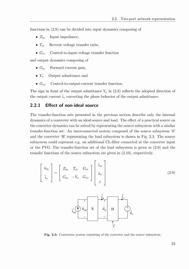
2.2 Two-port network representation . . . . . . . . . . . . . . . . . . . . . . . . 20
2.2.1 Effect of non-ideal source . . . . . . . . . . . . . . . . . . . . . . . . . . 23
2.2.2 Effect of non-ideal load . . . . . . . . . . . . . . . . . . . . . . . . . . . 26
2.3 Stability assessment of interconnected electrical systems . . . . . . . . . . . 28
2.4 Dynamic model of a photovoltaic generator . . . . . . . . . . . . . . . . . . 30
2.5 Dynamic model of a current-fed VSI-type converter . . . . . . . . . . . . . 33
2.5.1 Effect of photovoltaic generator . . . . . . . . . . . . . . . . . . . . . . 36
2.5.2 Comparison of current-fed and voltage-fed VSI . . . . . . . . . . . . . 40
2.6 Dynamic model of a current-fed semi-quadratic buck-boost converter . . . 43
3. Closed-loop formulation & control-system design . . . . . . . . . . . . 51
3.1 Input-voltage control . . . . . . . . . . . . . . . . . . . . . . . . . . . . . . 51
3.2 Output-current control . . . . . . . . . . . . . . . . . . . . . . . . . . . . . 54
3.3 Cascaded control scheme . . . . . . . . . . . . . . . . . . . . . . . . . . . . 57
3.4 Control-system design . . . . . . . . . . . . . . . . . . . . . . . . . . . . . . 59
3.4.1 VSI-type inverter . . . . . . . . . . . . . . . . . . . . . . . . . . . . . . 60
v

3.4.2 Semi-quadratic buck-boost-type inverter . . . . . . . . . . . . . . . . . 64
3.5 Negative output impedance in VSI-type inverter . . . . . . . . . . . . . . . 69
3.6 Input-capacitor selection of VSI-type inverter . . . . . . . . . . . . . . . . . 71
3.6.1 Input-voltage-ripple-based constraint . . . . . . . . . . . . . . . . . . . 72
3.6.2 Control-system-design-based constraint . . . . . . . . . . . . . . . . . . 73
4. Experimental measurements . . . . . . . . . . . . . . . . . . . . . . . . . 77
4.1 Photovoltaic generator & solar array simulator . . . . . . . . . . . . . . . . 77
4.2 VSI-based inverter . . . . . . . . . . . . . . . . . . . . . . . . . . . . . . . . 81
4.2.1 Input-voltage-control stability . . . . . . . . . . . . . . . . . . . . . . . 84
4.2.2 Negative output impedance . . . . . . . . . . . . . . . . . . . . . . . . 85
4.3 Semi-quadratic buck-boost-type inverter . . . . . . . . . . . . . . . . . . . . 88
5. Summary of the thesis . . . . . . . . . . . . . . . . . . . . . . . . . . . . 92
5.1 Final conclusions . . . . . . . . . . . . . . . . . . . . . . . . . . . . . . . . . 92
5.2 Future research topics . . . . . . . . . . . . . . . . . . . . . . . . . . . . . . 96
Bibliography . . . . . . . . . . . . . . . . . . . . . . . . . . . . . . . . . . . . 97
Appendices . . . . . . . . . . . . . . . . . . . . . . . . . . . . . . . . . . . . 111
A.Nominal and source-affected H-parameters of VSI-type converter . . 111
B.Nominal and source-affected H-parameters of CFSQBB converter . . 114
C.Closed-loop transfer functions of VSI-type PV inverter . . . . . . . . 120
D.Control-related transfer functions of CFSQBB PV inverter . . . . . . 122
E.Photographs of prototypes and measurement setup . . . . . . . . . . . 124
vi

SYMBOLS AND ABBREVIATIONS
ABBREVIATIONS
A Ampere
AC, ac Alternative current
CC Constant current
cc Current controller
CCR Constant current region (of a photovoltaic generator)
CF Current-fed (i.e. supplied by a current source)
CFSQBB Current-fed semi-quadratic buck-boost
CSI Current source inverter
CV Constant voltage
CVR Constant voltage region (of a photovoltaic generator)
DC, dc Direct current
dB Decibel
dBA Decibel-ampere
dBS Decibel-siemens
dBV Decibel-volt
dBΩ Decibel-ohm
G G-parameter model (i.e. voltage-to-voltage)
H H-parameter model (i.e. current-to-current)
Hz Hertz
L Load subsystem
LHP Left half of the complex plane
MPP Maximum power point
MPPT Maximum power point tracking
NPC Neutral-point clamped
OC Open circuit
p.u. Per unit value
PV Photovoltaic
PVG Photovoltaic generator
RHP Right half of the complex plane
S Source subsystem
SC Short circuit
SSA State space averaging
V Volt
vc Voltage controller
VF Voltage-fed (i.e. supplied by a voltage source)
VSI Voltage source inverter
vii

Y Y-parameter model (i.e. voltage-to-current)
Z Z-parameter model (i.e. current-to-voltage)
GREEK CHARACTERS
∆ Characteristic equation of a transfer function (determinant)
ωgrid Grid frequency (rad/s)
ωloop Control-loop crossover frequency (rad/s)
LATIN CHARACTERS
a Diode ideality factor
A State coefficient matrix A
B State coefficient matrix B
c Perturbed general control variable
C Capacitor or capacitance
C State coefficient matrix C
cpv Internal capacitance of a photovoltaic generator
d Duty ratio
d Pertured duty ratio
D Steady-state value of the duty ratio
D State coefficient matrix D
d′ Compelement of the duty ratio
D′ Compelement of the duty ratio in steady state
f General function in time domain
f-3dB Cut-off frequency of PV impedance magnitude curve
fsw Switching frequency
Ga Modulator gain
Gcc Current controller transfer function
Gci Control-to-input transfer function
Gco Control-to-output transfer function
Gio Forward (input-to-output) transfer function
Gse Voltage sensing gain
Gvc Voltage controller transfer function
i0 Diode reverse saturation current
iC Capacitor current
icpv Current through the capacitance cpvid Diode current
ig Grid current
iin Input current
iin Perturbed input current
iinS Perturbed source subsystem input current
viii

iinv Inverter input current
iL Inductor current
iL Perturbed inductor current
io Output current
io Pertured output current
ioL Pertured load subsystem output current
iph Photocurrent, i.e. current generated via photovoltaic effect
ipv Terminal (output) current of a photovoltaic generator
Ipv Photovoltaic generator operating-point current
irsh Current through the resistance rshIin Steady-state input current
IL Steady-state inductor current
Io Steady-state output current
I Identity matrix
k Boltzmann constant
kgrid Coefficient regarding the input-voltage-control bandwidth
ki Coefficient regarding the short-circuit current of a PVG
kRHP Coefficient regarding RHP pole in the input voltage loop
L Inductor or inductance
Lin Loop gain for input-voltage control loop
Lin Loop gain for intermediate-voltage control loop
Lout Loop gain for output-current control loop
Ns Number of series-connected cells in a photovoltaic generator
ppv Power of a photovoltaic generator
q Electron charge
rC Equivalent series resistance of a capacitor
rd Diode resistance (non-linear)
rds Drain-to-source resistance of a switch
rL Equivalent series resistance of an inductor
rpv Internal resistance of a photovoltaic generator
rs Internal series resistance of a photovoltaic generator
rsh Internal shunt resistance of a photovoltaic generator
Req Equivalent current-sensing resistor
s Laplace variable
S Switch component
t Time
T Temperature
Toi Reverse (output-to-input) transfer function
u(t) Input variable vector in time domain
u(t) Perturbed input variable vector in time domain
ix

ud Diode voltage
ug Grid voltage
uin Input voltage
uin Perturbed input voltage
uinS Perturbed source subsystem input voltage
uinv Inverter input voltage
uC Capacitor voltage
uL Inductor voltage
uo Output voltage
uo Pertured output voltage
uoL Pertured load subsystem output voltage
upv Terminal (output) voltage of a photovoltaic generator
Upv Photovoltaic generator operating-point voltage
uref Reference voltage
UC Steady-state capacitor voltage
Uin Steady-state input voltage
Uo Steady-state output voltage
U(s) Input variable vector in laplace domain
xin Perturbed input variable of interconnected system
x(t) State variable vector in time domain
x(t) Perturbed state variable vector in time domain
X(s) State variable vector in laplace domain
y(t) Output variable vector in time domain
y(t) Perturbed output variable vector in time domain
Yff Feedforward admittance
Y(s) Output variable vector in laplace domain
Yin Input admittance
yo Perturbed output variable of interconnected system
Yo Output admittance
YS Source admittance
Zin Input impedance
ZL Load impedance
Zo Output impedance
ZS Source impedance
SUBSCRIPTS
-∞ Ideal transfer function
1,2... Indexing numbers
-c Closed loop
grid Utility grid
x

loop Control loop
max Maximum
min Minimum
-o Open loop
-oco Open-circuited output
p pole (root of transfer function denominator)
pv Photovoltaic generator
RHP Right half of the complex plane
SA Source affected
-sci Short-circuited input
z Zero (root of transfer function nominator)
SUPERSCRIPTS
-1 Matrix inverse
G G-parameter model (i.e. voltage-to-voltage)
H H-parameter model (i.e. current-to-current)
im Intermediate or intermediate-voltage-control loop is closed
in Input or input-voltage-control loop is closed
io Output current
L Load subsystem transfer function
out Output current control loop is closed
out-in Output current and input voltage control loops are closed
S Source subsystem transfer function
SA Source-affected transfer function
uim Intermediate voltage
uin Input voltage
Y Y-parameter model (i.e. voltage-to-current)
Z Z-parameter model (i.e. current-to-voltage)
xi

1 INTRODUCTION
This chapter introduces the background of the research, clarifies the motivation for the
conducted research and reviews the existing knowledge related to the topic of the thesis
and the ideas presented in it. In addition, the structure, objectives and main scientific
contributions of the thesis are introduced.
1.1 Photovoltaic energy
Majority of global energy consumption is covered by non-renewable fuels, such as coal,
peat, oil, natural gas and nuclear. In 2009, 86.7 % of primary energy consumption and
80.5 % of electrical energy production was covered by the non-renewable fuels. The share
of hydropower in electrical energy production was 16.2 % while other renewable energy
sources covered only 3.3 % (IEA, 9.3. 2012).
The depletion of the non-renewable fuel supplies is a serious threat in the relatively
near future. Abbott (2010) estimates that at the current rate of consumption reasonably
recoverable coal reserves will run out in 130 years, natural gas in 60 years, oil in 40
years and uranium resources used in the nuclear energy production in 80 years. In
addition, Abbott reminds that oil, coal and gas are precious resources used in numerous
crucial industrial applications and physical products and thus should be conserved and
not burned.
The burning of the fossil fuels generates emissions that cause environmental pollution
and global warming, which is considered as one of the main issues of modern society.
The mitigation of the global warming problem, energy independency and securing the
availability of energy also in the future require the promotion of energy consumption in
electrical form, energy conservation and harnessing renewable energy resources such as
solar and wind (Barroso et al., 2010; Bose, 2010; Razykov et al., 2011).
Solar energy has enormous potential. Kroposki et al. (2009) estimate that the annual
global energy consumption of mankind is less than the energy the earth receives from
the sun in one hour. Solar radiation can be exploited as heat or converted directly into
electrical energy by means of photovoltaic (PV) conversion (Parida et al., 2011). A PV
cell is the basic building block of a PV generator (PVG). The low-voltage PV cells are
typically connected in series to form higher-voltage units known as modules, enabling
practical harvesting of the PV energy. The modules may be further connected in series
1

Chapter 1. Introduction
and parallel to form strings and arrays for utility-scale PV energy harvesting (Rahman,
2003).
Most of the commercial PV technology is based on silicon, which is the basic material
of modern electronics. Therefore, the manufactoring process of silicon is well-known and
the existing facilities enable large-scale commercial production of the silicon-based PV
cells. The efficiency of the silicon-based PV cells can be over 20 %, although higher
efficiencies have been achieved utilizing materials such as gallium and arsenic (Green
et al., 2012). Because the efficiency of the PVG is low, the interfacing-converter efficiency
is a vital aspect in the PV system design.
The first large-scale interest in the silicon-based PV technology since its invention
in 1955 emerged in the mid 1970s. The oil crisis and the increasing demand to use
PV technology in large telecommunication systems stimulated rapid development of the
module technology, resulting in the first modern PV modules (Green, 2005). The current
interest is to use the PV technology in grid-connected applications driven by the urge to
minimize environmental pollution and dependency on oil, positive price development of
renewable energy technologies and their public subventions (Rahman, 2003; Watt et al.,
2011).
The solar PV electricity has had the highest growth rate of all electrical energy pro-
duction with the annual increase of 33 % in production capacity. It has been estimated
that solar PV will be the second largest source of renewable electrical energy generation
after wind power around 2020, excluding hydropower, and the largest source around 2050
(Valkealahti, 2011). Valkealahti forecasts that the solar PV will be competitive without
subventions by mid 2030’s with an uncertainity margin of 10 years depending on the
geographical solar radiation conditions.
1.2 Photovoltaic generator as an input source
Simplified electrical equivalent circuit of a PV cell can be represented by a parallel con-
nection of a photocurrent iph, which is linearly proportional to the irradiation, and a
diode depicting the properties of the semiconductor junction as shown in Fig. 1.1. In
addition, the practical single-diode model of a PV generator includes shunt resistace rsh
and series resistance rs depicting losses in the cell (Liu and Dougal, 2002; Villanueva
et al., 2009). In Fig. 1.1, ipv is the PV cell terminal current, upv is the terminal voltage,
irsh is the current through the shunt resistance and id is the diode current.
The single-diode model can also be used to model the operation of a PV module,
i.e. a series connection of PV cells, by scaling the module parameters as presented by
Villanueva et al. (2009). According to Villanueva et al., the static terminal characteristics
2

1.2. Photovoltaic generator as an input source
phi du shr pvu
pvisr
rshidi
Fig. 1.1: Simplified electrical equivalent circuit of a PV cell.
0.0 0.2 0.4 0.6 0.8 1.0 1.20.0
0.2
0.4
0.6
0.8
1.0
1.2
Cu
rren
t, p
ow
er (
p.u
.)
Voltage (p.u.)
MPP
ipv
ppv
Fig. 1.2: Static terminal behavior of a PVG.
of a PV module can be given by
ipv = iph − i0
[
exp
(upv + rsipvNsakT/q
)
− 1
]
− upv + rsipvrsh
, (1.1)
where iph is the photocurrent generated by the irradiation, i0 is the diode reverse sat-
uration current, T is the temperature of the p-n junction in Kelvin, k is the Bolzmann
constant, a is the diode ideality factor, q is the electron charge and Ns is the number of
series-connected PV cells.
The static terminal characteristics are shown in Fig. 1.2 as a current-voltage (IV)
and power-voltage curves presented in normalized (p.u.) values. Fig. 1.2 shows that the
PVG is a power and voltage-limited current source. At voltages lower than the MPP, the
internal current-source property determines the terminal characteristics, i.e. the PVG
current ipv stays relatively constant despite changes in the operating point. At voltages
higher than the MPP, the PVG voltage (and thus also power) is limited due to the
forward biasing of the diode in Fig. 1.1 and the PVG has the properties resembling a
voltage source, i.e. the PVG voltage stays relatively constant despite the changes in the
operating point.
3

Chapter 1. Introduction
0.0 0.2 0.4 0.6 0.8 1.0 1.20.0
0.2
0.4
0.6
0.8
1.0
1.2
Curr
ent
(p.u
.)
Voltage (p.u.)
25°C
50°C
500 W/m2
1000 W/m2
Fig. 1.3: Static terminal behavior of a PVG at varying irradiance and temperature.
In order to maximally utilize the energy of solar radiation by using a PVG, its oper-
ating point should constantly be kept at the maximum power point (MPP, Fig. 1.2), in
which
dppvdupv
=d(upvipv)
dupv
= Ipv + Upv
dipvdupv
= 0, (1.2)
where Ipv and Upv are the MPP current and voltage. Esram and Chapman (2007) have
reviewed various algorithms used for MPP-tracking (MPPT) that has to be implemented
in order to locate the MPP along the PVG IV-curve.
In Eq. (1.1), the p-n junction temperature is in the denominator of the power of the
exponential function, which can be used to determine the open-circuit voltage. Accord-
ingly, a PVG provides more power at lower temperatures. The temperature and irradi-
ance dependency of a PVG is depicted in Fig. 1.3. The open-circuit voltage is mostly
determined by the temperature and the short-circuit current by the solar radiation.
1.3 Grid-connected photovoltaic systems
The grid-integration of a PVG requires a power electronic interface, an inverter. Power
electronics is a key technology in a sustainable energy future by enabling efficient energy
conversion and grid integration of renewable energy sources (Blaabjerg et al., 2004; Car-
rasco et al., 2006; Popovic-Gerber et al., 2011). Popovic-Gerber et al. have studied the
energy payback times of power electronic systems and conclude that power electronics
does not only enable the grid-integration of renewable energy sources but also offers vast
energy saving potential e.g. in motor drives and lighting. Harnessing such a potential is
crucial in achieving sustainable energy future.
4

1.3. Grid-connected photovoltaic systems
According to Blaabjerg et al., the way to fully exploit the renewable energy sources
is the grid connection, where the power electronics plays a vital role in matching the
grid-connection requirements and the intermittent nature of the renewables. The basic
rule in the power grid is that the consumption and production of electrical energy match
all the time. The output power of the renewables, on the other hand, is determined e.g.
by environmental conditions. Carrasco et al. discuss the future urge to utilize energy
storing technologies in order to store excess renewable energy and utilize it during the
low-production conditions. Kakimoto et al. (2009) have proposed a ramp-rate-control
scheme utilizing stored energy in order to level out the varying PV inverter output due
to moving clouds.
Each grid-connected PV conversion system composes of at least the inverter, but may
also contain an additional dc-dc converter used as an upstream converter between the
PVG and the inverter forming a two-stage conversion scheme. The use of the additional
dc-dc stage enables the use of PV string composed of less series-conncted PV modules
compared to single-stage conversion scheme, which may be beneficial in case of partial
shading conditions (Maki and Valkealahti, 2012). The dc-dc stage can also regulate its
input voltage to practically pure dc (i.e., it provides perfect power decoupling), which
according to Wu et al. (2011) can compensate the energy losses caused by single-phase
power fluctuation affecting especially the single-stage single-phase inverters. The grid-
connected PV inverters are subjected to high expectations and requirements. According
to Araneo et al. (2009); Eltawil and Zhao (2010), the PV inverters should have
• high conversion efficiency,
• high-accuracy MPP-tracking facility,
• long life span,
• high quality of injected power,
• reduced cost, size and weight
• and comply with all the required standards for the grid interfacing.
1.3.1 Photovoltaic inverter concepts
The most common concepts of interfacing PVG to the utility grid are shown in Fig. 1.4.
In the modular concept shown in Fig. 1.4a, each PV module is interfaced to the grid with
a dedicated micro inverter. Typically the micro inverter adopts the two-stage conversion
scheme since the input-voltage requirement of a typical single-phase inverter is at least
the peak grid voltage with a sufficient margin, and the MPP voltage of a typical module
is in the order of a few tens of volts. Matching such a high voltage difference requires
5

Chapter 1. Introduction
N
3L2L1L
( )a ( )b ( )c ( )d
Fig. 1.4: a) Module-integrated, b) string, c) multistring and d) central inverter concepts.
the use of converter topologies with high conversion ratio (Kjaer et al., 2005; Li and He,
2011). The modular concept has good expandability and high MPP tracking efficiency
due to dedicated MPP-trackers for each module (Liu et al., 2011; Roman et al., 2006).
The disadvantage of the modular concept is the high conversion ratio requirement, which
has a negative effect on the conversion efficiency.
The relatively high PV voltage required for the single-stage inverter can be achieved
by connecting PV modules in series, forming the PV string. The string-inverter concept
is shown in Fig. 1.4b. The string inverters are characterized by simplicity and high
efficiency. The string inverter is one of the most interesting concepts in small-scale
PV power production such as residential rooftop applications (Araujo et al., 2010; Liu
et al., 2011; Myrzik and Calais, 2003; Schonberger, 2009). The disadvantage of the
string inverter concept is the increased propability of partial shading of the long PV
string, especially in the built environment, which may significantly reduce the energy
production.
The multistring-inverter concept using the additional dc-dc stages is shown in Fig. 1.4c.
Each of the dc-dc stages fed by individual PV strings are connected to the inverter input
terminals in a parallel configuration. The combined power of the multiple short strings
may require the use of a three-phase inverter topology (Araujo et al., 2010). A modular
dc-dc conversion scheme can be derived from the multistring-inverter concept, where each
of the short strings is replaced by a single PV module (Zhang et al., 2011).
In the central-inverter concept shown in Fig. 1.4d, the inverter is fed by a parallel
connection of long PV strings forming a high-power PV array. The central inverter
concept was popular in the early grid-connected PV systems and is still typically used in
dedicated high-power PV plants. The strings are typically equipped with series-connected
6

1.3. Grid-connected photovoltaic systems
diodes in order to prevent negative power flow in the strings, because in partial shading
conditions the non-shaded strings could inject power to a shaded string possibly damaging
it. Most of the central inverters are three-phase inverters, although some single-phase
products exist in the PV market according to Araujo et al. (2010). Araujo et al. also
mention a minicentral concept, which is based on three single-phase string inverters
forming a three-phase system. Its main advantage is that the input-voltage requirement
of a single-phase inverter is reduced compared to three-phase topologies, allowing the use
of higher efficiency topologies and shorter PV strings.
Most of the PV inverters are based on the voltage-source-inverter (VSI) topology,
although the use of current-source-inverter (CSI) topology is proposed e.g. by Sahan
et al. (2011). The VSI-based multilevel inverter is also an emerging application, whose
main advantages, according to Calais et al. (1999), are low grid-current ripple and the
ability to use lower-voltage-rating components. However, this thesis mainly studies the
VSI-based inverter. A review of various topologies for single-phase grid interfacing of
renewable resources can be found e.g. in (Lai, 2009).
1.3.2 Single- and two-stage conversion schemes
A single-stage grid-connected PV conversion scheme is shown in Fig 1.5a. The single-
stage PV inverter employs a cascaded control scheme, where an inner grid-current-
feedback loop controls the grid current and an outer input-voltage-feedback loop controls
the input voltage by generating the grid-current reference (Yazdani and Dash, 2009).
The grid-current reference must be synchronized with the grid voltage (Sync.) utilizing
some of the various existing grid synchronization methods (Teodorescu et al., 2011). The
current controller is denoted by cc and voltage controller by vc in Fig 1.5a. The input-
voltage reference is generated by the MPPT facility. The grid-current control is a must
in grid-connected applications in order to inject high quality power to the grid.
MPPT
Sync
cc
gu
PVGInverter
vc
inu
giini
ref
inu
(a) Single-stage.
invu
Sync
cc
gu
Inverter
invvc
gi
ref
invuMPPT
PVG
invc
inu
ini
ref
inu
invidc-dc
(b) Two-stage.
Fig. 1.5: Single and two-stage PV conversion schemes.
7
Chapter 1. Introduction
A two-stage grid-connected PV conversion scheme is shown in Fig 1.5b. In the two-
stage conversion scheme, the inverter again controls its input voltage by means of the
cascaded control scheme. The input-voltage controller of the inverter is denoted by vcinv
and the input-voltage controller of the dc-dc stage by vcin in Fig 1.5b. The inverter input-
voltage reference in the two-stage conversion scheme is constant (i.e., proportional to the
grid voltage) compared to the varied input-voltage reference of the single-stage scheme.
The dc-dc converter in the two-stage scheme is responsible for the MPPT function, either
by controlling its input voltage or current, or by operating at open loop (Khalifa and
El-Saadany, 2011; Masoum et al., 2002).
In PV applications, the input-current control is prone to saturation, since the MPP
current is close to the short-circuit current that is dependent on the irradiation level
with relatively fast dynamics. The open-circuit voltage, on the other hand, is dependent
mostly on the temperature with negligibly slow dynamics, thus input-voltage control can
be realized in a reliable manner (Xiao et al., 2007). It has been studied by Messo et al.
(2012) that the input-voltage control of the dc-dc pre-regulator transforms its output
into a constant-power-type source, which is beneficial for the inverter. Therefore, the
input-voltage control is also recommended over the open-loop-based MPPT.
Some authors claim that the dc-dc converter in the two-stage conversion scheme could
be used to control the dc-link voltage (Kwon et al., 2006; Liao and Lai, 2011; Vighetti
et al., 2012). However, it has been proven e.g. by Leppaaho et al. (2010); Nousiainen
et al. (2011b); Puukko et al. (2012), that an output-side control, be it output current or
voltage, cannot draw maximum power out of a PVG without compromising the stability,
as will also be shown in this thesis. Thus, input-voltage control should always be used.
This implies that the PVG-interfacing converters are current-fed converters instead of
traditional voltage-fed converters (Capel et al., 1983). The correct identification of the
controlled variables in a PV converter is of utmost importance, because the dynamic
formulation of a converter is based on the selection of controlled variables (system out-
puts) and uncontrollable variables (system inputs), where the transfer-function set of the
converter describes the relation between the system inputs and outputs (Suntio, 2012).
The dynamic formulation of a PV converter is discussed in detail later in this thesis.
1.4 Issues on single-phase photovoltaic systems
Electricity generation has been centralized in large power plants until the recent develop-
ment towards distributed energy generation. The rapidly increasing penetration level of
the dispersed power generation, such as relatively small-power PV plants, has increased
concerns about the reliability and quality of the electricity supply (Bletterie and Brunner,
2006; Braun et al., 2011). Bletterie and Brunner define reliability by the number and
duration of power interruptions and power quality by the distortions, such as harmon-
8

1.4. Issues on single-phase photovoltaic systems
ics, voltage dips or flicker. According to Braun et al., the PV inverters have adopted a
passive approach in the grid connection, but in the future should actively participate in
grid control in order to maintain reliable and high-quality electricity supply without the
need for excess grid reinforcements, and to keep the costs of PV grid integration low.
In the passive grid-connection approach, PV inverters are required to inject high
quality active power and disconnect from the grid upon detection of e.g. over- or un-
dervoltage, excess grid frequency deviation or detection of an islanding situation in the
grid (Ciobotaru et al., 2010). When the number of PV systems in the grid is high, such
voltage and frequency deviations might disconnect a large portion of power production
off the grid leading to an unrecoverable violation of the power balance and total loss of
electricity supply. The energy stored in the inertia of traditional spinning generators has
maintained grid integrity during the violations of the power balance, which is reflected
as small deviations of the grid frequency that can be fixed by adjusting the amount of
power production (Bebic et al., 2009).
In the active approach, the PV inverter’s ability to supply real and reactive power
is utilized in order to provide grid voltage and frequency supporting functions (Braun
et al., 2011; Carnieletto et al., 2011). Carnieletto et al. have reviewed control methods
to realize such functions in a single-phase photovoltaic inverter. It might not be feasible
to disconnect a large PV plant from the grid in case of an islanding situation but let
the PV plant maintain the grid by itself. Methods to cope with intended islanding have
been studied e.g. by Nian and Zeng (2011); Vasquez et al. (2009); Yao et al. (2010). The
dynamic formulation of the PV inverter presented in this thesis can be helpful in order
to study the dynamic properties of the supporting functions or the islanding situation,
although the developement of such a functionality is out of the scope of this thesis.
Chicco et al. (2009) has observed that harmonic distortion in the grid voltage excites
harmonic-current pollution in a PV inverter. They have reported linear increase in the
harmonic current as a function of grid harmonic voltages. This implies that PV inverters
have finite output impedances at the relevant harmonic frequencies. In order to study
such interactions, a dynamic model of the output impedance is required, because the
time-domain analyses cannot explain such a behavior. This emphasizes the importance
of the PV-inverter modeling in the frequency domain. Chicco et al. have also observed
that the highest current distortion occurs in low-power conditions, i.e. in cloudy weather
or at sunrise and sunset. Simmons and Infield (2000) assume that this is caused by the
limited resolution of the grid-current measurement and control. Bhowmik et al. (2003)
have studied the maximum allowable penetration of the distributed-generation-related
inverters in the grid based on the harmonic pollution limits.
The efficiency of a PV inverter system is not merely determined by the inverter ef-
ficiency, but also by the MPP efficiency (Bletterie et al., 2011). The MPP efficiency is
9

Chapter 1. Introduction
defined as a fluctuation of the operating point around the MPP that is caused by the
inverter input-voltage ripple or inaccuracy of the MPP-tracking facility. The voltage rip-
ple is caused either by the converter switching actions or the inherent power fluctuation
at twice the grid frequency in single-phase power grid (Benavides and Chapman, 2008;
Sullivan et al., 2011). The voltage ripple at twice the grid frequency may be mitigated
by connecting a large capacitor at the input terminal of the inverter (Liserre et al., 2004;
Prapanavarat et al., 2002) and by applying passive (Nonaka, 1994) or active power de-
coupling techniques (Hu et al., 2010; Shimizu et al., 2006; Tan et al., 2007; Vitorino and
de Rossiter Correa, 2011). Input-voltage can be also controlled practically to dc by a
pre-regulator, which provides perfect power decoupling as discussed earlier.
The most unreliable part of a PV system has been observed to be the inverter (Chan
and Calleja, 2011; Petrone et al., 2008), and the most unreliable component in the inverter
is the large electrolytic power decoupling capacitor (Bower et al., 2006; Kotsopoulos et al.,
2001; Ninad and Lopes, 2007; Rodriguez and Amaratunga, 2008). The possibility to use
a small capacitor would allow the use of other types of capacitors than electrolytics,
which would increase inverter reliability. However, the issues related to the small energy-
storage capacitors need to be solved (Chen et al., 2009; Chen, Wu, Chen, Lee and Shyu,
2010; Fratta et al., 2002). According to Fratta et al. (2002), the minimization of the
input capacitor can lead to sub-harmonic oscillations in the inverter or even instability.
In this thesis, the minimum allowed input capacitance for the single-phase PV inverter
is derived based on the input-voltage-control stability.
1.4.1 Grid interactions
The inverters related to distributed generation have been observed to generate harmonic
current pollution, excite harmonic resonances in the grid or even cause instability, es-
pecially, in weak grid conditions (Cespedes and Sun, 2009, 2011; Chen and Sun, 2011;
Enslin and Heskes, 2004; Heskes et al., 2010; Liserre et al., 2006; Mohamed, 2011; Sun,
2008; Wang et al., 2011). Such issues can be most conviniently studied based on inverter
and grid impedances. It is well known that the stability of an interconnected voltage-fed
system can be assessed by applying the Nyquist stability criterion to the impedance ratio
of the load and source subsystems known as minor-loop gain (Zo/Zin), where Zo is the
output impedance of the source subsystem and Zin is the input impedance of the load
subsystem (Middlebrook, 1976). The stability of a current-fed system can be assessed by
the inversion of the minor-loop gain (Zin/Zo) (Leppaaho et al., 2011; Sun, 2011). Typ-
ically the stability criterion is used to study the stability of the inverter/grid interface,
but it naturally also applies to the PVG/inverter interface.
If the impedance ratio of an interconnected system consisting of independently stable
source and load subsystems does not satisfy the Nyquist stability criterion, the inter-
10

1.4. Issues on single-phase photovoltaic systems
connected system is unstable. It can be deduced that the impedance-based stability
criterion will be violated in a PV system if |Zin/Zo| ≥ 1 while the phase difference of the
impedances exceed 180 degrees. Therefore, it is obvious that problems can be expected
when the grid impedance is high (weak grid conditions), as reported e.g. by Liserre et al.
(2006). Likewise, Caamano-Martin et al. (2008) reports that PV inverters do not con-
tribute to the harmonic current pollution in strong networks (i.e. the grid impedance is
low). The concept of minor-loop gain can be used to determine the stability of the inter-
face between the inverter and the utility grid (Cespedes and Sun, 2009; Sun, 2011), but it
can also be used to study the harmonic resonance problem (Chen and Sun, 2011; Wang
et al., 2011). Wang et al. propose that the standards regarding distributed generation
inverters should include limits for the minimum inverter output impedance.
If the source and load subsystem impedances show passive-circuit-like behaviour, i.e.
the impedance phase lies between ±90, the violation of the stability criterion requires
undamped circuits. Accordingly, the passive-circuit-like behavior can excite harmonic
resonances, but a complete loss of stability requires active-circuit-like behaviour in the
inverter output impedance. Therefore, it is obvious that negative-resistor-like behavior
(phase is −180) in the inverter output impedance exposes the inverter/grid interface to
instability (Heskes et al., 2010). One of the origins of the negative-resistor-like behav-
ior is the grid synchronization (Cespedes and Sun, 2011; Enslin, 2005). Enslin implic-
itly concludes that grid-synchronization where the shape of the grid voltage is used to
shape the grid current reference results in negative-resistor-like behavior. In this thesis,
such a multiplier-based synchronization is analyzed and an additional negative-output-
impedance term caused by the synchronization is explicitly formulated.
1.4.2 Ground-leakage current
The PV modules have a high surface area forming relatively high parasitic capacitance
between the module and its framing. According to Calais et al. (1999), the parasitic
capacitance might be up to several nanofarads per module. The PV module installation
is typically connected to the system ground. Therefore, a path between the dc-side
and the neutral conductor exists allowing possible ground-leakage current to flow (also
known as common-mode current). The ground-leakage current is owing to a high rate-of-
change of voltage (du/dt), known as common-mode voltage, induced accross the ground
capacitance by the inverter switching actions, which creates the ground-leakage current
according to iC = C · duC/dt. The ground current is limited by standards and may
decrease the lifetime of the PV module and the inverter efficiency as well as distort grid
current and cause electromagnetic interference (Gubia et al., 2007; Lopez et al., 2010;
Xiao and Xie, 2010). According to Bower and Wiles (2000), the ground-leakage current
may become large enough to indicate a ground fault and cause unwanted tripping of
11

Chapter 1. Introduction
safety equipment. Such false indications of ground faults can have a significant effect on
the system down time (Caamano-Martin et al., 2008).
Three possible methods exist to mitigating the ground-leakage current. The first
method is not to ground the PV module framing. However, in case of common mode
voltage generated by the inverter between the PVG terminals and the power system
grounding, a person touching a PV module is exposed to an electric hazard. Such safety
concerns can be eliminated by grounding the module installation. Accoding to Lopez
et al. grounding of the PVG installation is mandatory in the U.S. and in some countries
in Europe. Secondly, the galvanic path could be disconnected using a transformer. A
low-frequency transformer connected between the inverter and the grid is large, expen-
sive, heavy and has low efficiency. Therefore, it is not a desired method to solve the
ground-current problem, although it also blocks the dc-current that increases the risk of
saturation in distribution transformers and is limited by standards (Brundlinger et al.,
2009; Salas et al., 2008). A small and cheap transformer can be used integrated into a
transformer-isolated dc-dc converter used as the pre-regulator (Kjaer et al., 2005). The
third method is to use a topology or modulation method that excites minimal ground
current to flow. Transformerless inverters are stated to be the key technology for simple,
efficient and low-cost grid integration of a PVG. A lot of research effort has been devoted
to the development of the transformerless inverters (Barater et al., 2009; Gonzalez et al.,
2008, 2007; Kerekes et al., 2011; Xiao et al., 2011; Xue et al., 2004; Yang et al., 2012; Yu
et al., 2011).
The transformerless inverter topologies are typically based either on the conventional
half-bridge (Fig. 1.6a) or full-bridge inverter (Fig. 1.6b) that are also referred to as
VSI-type topologies. In the half-bridge inverter, the neutral conductor is connected
between two capacitors dividing the input-side voltage. Thus, the voltage accross the
parasitic ground capacitance is determined by the voltages of capacitors C1 and C2
in Fig. 1.6a. The capacitor voltages, and therefore the ground voltage, are ideally dc
and practically no ground current flows (Kerekes et al., 2007). However, the input or
gu
PVG inu
ini
1C
2C
giL
(a) Half-bridge.
guPVG inu
ini
C
giL
(b) Full-bridge.
Fig. 1.6: Typical VSI-type single-phase PV inverters.
12

1.4. Issues on single-phase photovoltaic systems
dc-link voltage requirement is twice the requirement of the full-bridge inverter. The half-
bridge is also a ‘two-level’ topology, i.e. the voltage between the switches can be either
negative or positive dc-voltage, which increases the output-current ripple and decreases
the efficiency. A variation of the half-bridge, known as neutral-point-clamped inverter
(NPC), is proposed that employs ‘three-level’ switching (negative, positive and zero)
(Calais et al., 1999). However, the NPC suffers from the high input-voltage requirement
and voltage balancing of the capacitors complicates the control-system design (Celanovic
and Boroyevich, 2000).
The full-bridge inverter enables both three-level and two-level switching. Even though
the two-level switching mitigates the ground-leakage current, it requires large grid-side
inductor L and lowers the inverter efficiency. The three-level switching, however, is
not suited for a transformerless inverter due to pulsating common-mode voltage at the
switching frequency (Kerekes et al., 2007). A feasible concept that can be used to build
a ‘three-level’ transformerless PV inverter is the concept based on unfolding inverter
switching at the grid frequency as shown in Fig. 1.7 (Chiang et al., 2009; Erickson and
Rogers, 2009; Kang et al., 2005; Li and Wolfs, 2008; Park et al., 2006; Prapanavarat et al.,
2002; Rodriguez and Amaratunga, 2008; Tofoli et al., 2009). The unfolder is operated in
such a manner that the control signal cp is high and cn is low during positive grid cycle
and vice versa during negative grid cycle. In addition, the inverter in Fig. 1.7 composes of
an additional dc-dc converter whose output current io is controlled according to full-wave
rectified grid voltage, which is ‘unfolded’ into sinusoidal grid current ig. Because of its
low switching frequency, the unfolder basically only exhibits conduction losses yielding
low total losses in the unfolder. The inverters analyzed in this thesis are based on the
unfolding-inverter concept. A review of various transformerless PV inverters can be found
e.g. in (Teodorescu et al., 2011).
guPVG inu
ini
C
gi
L
ou
oi
Polaritycontrol
pcnc
gu
Fig. 1.7: VSI-type PV inverter based on unfolding inverter.
13

Chapter 1. Introduction
1.4.3 Partial shading of photovoltaic generator
As discussed earlier, the string inverters are characterized by high efficiency enabled
by the development of various transformerless topologies, while micro inverters slightly
lack efficiency due to wide current and voltage-conversion-ratio requirement and multiple
power-conversion stages. However, the proper operation of a PV string requires uniform
operating conditions. In a long string, mismatch losses in the modules increase and partial
shading compromises the energy yield, especially in the built environment (Garcia et al.,
2008; Maki et al., 2011; Ramabadran and Mathur, 2009).
Partial shading generates multiple local maximum power points (MPP) to the power-
voltage curve of the string as shown in Fig. 1.8, where one third of a PV module with
three bypass diodes is shaded. When the shading intensity is low, the global maximum
power is found at higher voltages, but when the shading intensity increases, the global
MPP is found at low voltages, which might be outside the VSI-type inverter input-voltage
range, and therefore, impossible to obtain. It is a demanding task for a tracking algorithm
to locate a global MPP among the local maxima (Esram and Chapman, 2007; Kobayashi
et al., 2006; Patel and Agarwal, 2008). In general, algorithms without special intelligence
track the first maximum they find, whether it is local or global. This has been measured
to cause significant energy losses in a string inverter system in addition to the decreased
irradiance (Brundlinger et al., 2006).
The number of the local maxima in the power-voltage curve is defined by the bypass-
diode configuration: the number of possible MPP’s is the number of bypass-diodes in a
0.0 0.2 0.4 0.6 0.8 1.0 1.2 1.40.0
0.2
0.4
0.6
0.8
1.0
1.2
Voltage (p.u.)
Curr
ent
(p.u
.)
ipv
ppv
60 %
30 %
0 %
Shading intensity
Fig. 1.8: Static terminal characteristics of a partially shaded PVG.
14

1.5. Structure of the thesis
module multiplied by the number of modules in series, making the proper exploitation
of a string in case of partial shading difficult (Silvestre et al., 2009). The issue of partial
shading is an important topic that has been researched e.g. by (Deline, 2009; Maki and
Valkealahti, 2012; Wang and Hsu, 2010; Woyte et al., 2003).
In a modular system, MPP-tracking is performed on a module level, which minimizes
the effect of non-uniform operating conditions of the modules. It has been shown that
individual modules in parallel can outperform the series-connected string (Oldenkamp
et al., 2004). The modularity can be realized in a dc-dc system (Liu et al., 2011) or by
directly connecting each module to the ac grid by the micro-inverters. It has been shown
that a micro-inverter system can outperform conventional string-inverter system despite
lower efficiency, especially in the shaded conditions (Mohd, 2011). The potential energy
yield increase is the single most important reason for modular power electronics applied
in PV systems (Brundlinger et al., 2011).
Another advantage of a micro-inverter system is the modularity itself. The inverters
have been observed to be one of the most unreliable parts of a PV energy system as
discussed. In case of micro inverter failure, other modules in the system still provide
power to the grid while failure of a string inverter seizes energy production of the string
completely. The modular architecture provides straightforward expandability and re-
duces cost of initial investment. The micro inverter system is also free of high voltage dc
wiring, switch boxes and protection devices, which substantially lowers the installation
cost (Mohd, 2011). Various micro-inverter concepts has been studied e.g. by (Choi and
Lee, 2012; Kwon et al., 2009; Li and Oruganti, 2012; Rodriguez and Amaratunga, 2008;
Shimizu et al., 2006; Xue et al., 2004; Yu et al., 2011).
In this thesis, a new semi-quadratic buck-boost-type (CFSQBB) converter is proposed
that can be used as such in a dc-dc system or used to realize a transformerless micro
inverter utilizing the unfolder concept.
1.5 Structure of the thesis
In Chapter 2, the dynamic formulation of switching converters and dynamic modeling
of PV systems is presented and the effect of nonideal source and load on a PV con-
verter dynamics is formulated. Chapter 2 also presents dynamic models for the VSI- and
CFSQBB-type inverters in addition to the dynamic model of a PVG.
Chapter 3 formulates the closed-loop dynamics of PV converters and the control-
system designs of VSI- and CFSQBB-type inverters are presented. The closed-loop
analysis reveals the property of negative-resistor-like output impedance caused by the
cascaded control scheme, which is amplified by the multiplier-based grid synchroniza-
tion. The design of the input-voltage control in the cascaded control scheme is derived
based on the observed right-half-plane pole (RHP) in the control loop. The frequency of
15

Chapter 1. Introduction
the RHP pole is further used to formulate the design rule for minimum input capacitance
in a single-phase single-stage PV inverter.
Chapter 4 presents experimental results and Chapter 5 summarizes the thesis and
proposes important future research topics in PV inverters.
1.6 Objectives and scientific contribution
The objective of this thesis is to provide a dynamic formulation for the single-phase PV
inverter and reveal the origin of some of the problems discussed. The dynamic modeling
provides a powerful tool for deterministic control-system design and system-interaction
and stability analyses of the interconnected systems. The basic principles presented
in this thesis can be used to analyze various control practices emerging in the field of
PV inverters and other renewable energy technologies based on power electronics. The
scientific contribution of this thesis can be summarized as
• Explicit formulation of photovoltaic inverter modeling.
• Effect of photovoltaic generator on a single-phase VSI-type inverter dynamics.
• Design rule for the minimum input capacitance of a VSI-type photovoltaic inverter
based on input-voltage-control stability.
• Explicit formulation of the effect of multiplier-based grid synchronization causing
negative output impedance.
• Invention and development of a current-fed semi-quadratic buck-boost-type con-
verter topology suited for transformerless modular photovoltaic applications.
1.7 Related papers and authors contribution
The ideas presented in this thesis are published in the following scientific publications.
[P1] T. Suntio, J. Leppaaho, J. Huusari, L. Nousiainen, ”Issues on solar-generator inter-
facing with current-fed MPP-tracking converters,” IEEE Trans. Power Electron.,
vol. 25, no. 9, pp. 2409-2419, Sept. 2010.
[P2] J. Leppaaho, J. Huusari, L. Nousiainen, J. Puukko, T. Suntio, ”Dynamic proper-
ties and stability assessment of current-fed converters in photovoltaic applications,”
IEEJ Trans. Ind. Appl., vol. 131, no. 8, pp. 976-984, 2011.
[P3] L. Nousiainen, T. Suntio, ”Current-fed converter with quadratic conversion ratio,”
Patent Application, US2012007576, EP2408096, CN102332821, 2012.
[P4] L. Nousiainen, T. Suntio, ”Current-fed converter,”Patent Application, US2012008356,
EP2408097, CN102332840, 2012.
16

1.7. Related papers and authors contribution
[P5] L. Nousiainen, T. Suntio, ”Dual-mode current-fed semi-quadratic buck-boost con-
verter for transformerless modular photovoltaic applications,” 14th European Conf.
on Power Electronics and Applications (EPE), Birmingham, U.K., Aug./Sept. 2011,
pp. 1-10.
[P6] L. Nousiainen, T. Suntio, ”Dynamic characteristics of current-fed semi-quadratic
buck-boost converter in photovoltaic applications,” 3rd IEEE Energy Conversion
Congr. and Expo. (ECCE), Phoenix, Arizona, U.S., Sept. 2011, pp. 1031-1038.
[P7] L. Nousiainen, T. Suntio, ”Simple VSI-based single-phase inverter: dynamical effect
of photovoltaic generator and multiplier-based grid synchronization,” IET Renew-
able Power Generation Conf. (RPG), Edinburgh, U.K., Sept. 2011, pp. 1-6.
[P8] L. Nousiainen, T. Suntio, ”DC-link voltage control of a single-phase photovoltaic
inverter,” IET Power Electronics, Machines and Drives Conf. (PEMD), Bristol,
U.K., March 2012, pp. 1-6.
[P9] L. Nousiainen, J. Puukko, T. Suntio, ”Appearance of a RHP-zero in VSI-based
photovoltaic converter control dynamics,” 33rd Int. Telecommunications Energy
Conf. (INTELEC), Amsterdam, Netherlands, Oct. 2011, pp. 1-8.
[P10] J. Puukko, L. Nousiainen, T. Suntio, ”Effect of minimizing input capacitance in VSI-
based renewable energy converters,” 33rd Int. Telecommunications Energy Conf.
(INTELEC), Amsterdam, Netherlands, Oct. 2011, pp. 1-9.
[P11] J. Puukko, L. Nousiainen, A. Maki, J. Huusari, T. Messo, T. Suntio, ”Photovoltaic
generator as an input source for power electronic converters,” 15th Int. Power
Electronics and Motion Control Conf. and Expo. (EPE-PEMC), Novi Sad, Serbia,
Sept. 2012.
[P12] L. Nousiainen, J. Puukko, A. Maki, T. Messo, J. Huusari, J. Jokipii, J. Viinamaki,
D. Torres Lobera, S. Valkealahti, T. Suntio, ”Photovoltaic generator as an input
source for power electronic converters,” accepted for publication in IEEE Trans.
Power Electron., DOI: 10.1109/TPEL.2012.2209899.
In publications [P1]-[P2], the author helped with experiments and analyses. The
patent applications [P3]-[P4] are based on the new converter topologies by the author,
where the second author and the supervisor of this thesis, Professor Suntio, helped in
writing the patent proposals. Professor Suntio also gave useful comments and insight
regarding the theoretical and experimental findings in the publications [P5]-[P6], ana-
lyzing the converter in [P4] and analyzing the dynamic properties of the VSI-type PV
inverter in the publications [P7]-[P8]. The ideas behind publications [P9]-[P10] are a
17

Chapter 1. Introduction
collaboration with M.Sc. Puukko, who was responsible for the writing of [P10] and the
author was responsible for the writing of [P9]. The author had significant contribution in
the measurements and writing of [P11] and wrote the additional part of [P12] compared
to [P11].
18

2 DYNAMIC MODELING OF PHOTOVOLTAIC
CONVERTERS
In order to overcome the issues discussed earlier, a frequency-domain model of a PV
converter is of great advantage. The frequency-domain (i.e. small-signal) model describes
the relation between the converter input and output variables, also known as system
inputs and outputs. Such models describe e.g. the relation between the control (i.e.
duty ratio) and system outputs, which is needed in the control-system design, or the
impedance behavior of the converter, which is important in order to study the grid
interactions as discussed earlier.
2.1 State-space averaging
A conventional method to model a power electronic converter is the state-space averag-
ing method (Middlebrook and Cuk, 1977; Suntio, 2009). In the state-space averaging,
the converter operation is first averaged over a switching cycle with common average
integral. The averaged derivatives of state variables 〈x (t)〉 and system outputs 〈y (t)〉are represented as a function of the state variables and system inputs 〈u (t)〉 as shown
in (2.1), where the variables in angle brackets denote the average values and bold italics
mean vectors. The state variables are conveniently the capacitor voltages and inductor
currents. The system inputs and outputs are voltages and currents either at the load or
source side. Also a control variable is a system input.
d 〈x (t)〉d (t)
= f1 (〈x (t)〉 , 〈u (t)〉)
〈y (t)〉 = f2 (〈x (t)〉 , 〈u (t)〉)
(2.1)
In case of switching converters, the average-valued equations are non-linear and have
to be linearized at a steady-state operating point. The standard linearized state-space
representation is shown in (2.2) in the time domain and in (2.3) in the frequency domain.
The hat over the variables denote small-signal deviation around the steady-state value
19

Chapter 2. Dynamic modeling of photovoltaic converters
and the bold letters mean matrices.
dx (t)
d (t)= Ax (t) +Bu (t)
y (t) = Cx (t) +Du (t)
(2.2)
sX (s) = AX (s) +BU (s)
Y (s) = CX (s) +DU (s)(2.3)
The relation between the controllable output variables and uncontrollable input variables
in the frequency domain can be solved using (2.3) applying basic matrix algebra as given
in (2.4).
Y (s) =(C(sI−A)-1B+D
)U (s) = GU (s) (2.4)
The contents of the tranfer-function matrix G in (2.4) depend on the selection of
the input and output variables. According to Suntio et al. (2011), two basic converter
structures can be formed depending on the characteristics of the input power supply.
If the converter is fed from a stiff current source or the input voltage is controlled,
the source-side system input is the input current. If the converter is fed from a stiff
voltage source or the input current is controlled, the source-side system input is the
input voltage. Accordingly, Suntio et al. categorize converters into current-fed (CF) and
voltage-fed (VF) converters.
2.2 Two-port network representation
The CF and VF converters can be further divided according to their load mode, be it
voltage-type load or a current sink. Consequently, four possible conversion structures
exist that can be represented by the transfer function set given in (2.4). The transfer
function sets can be equally represented by linear two-port network models, which is a
common practice in circuit theory (Tse, 1998). According to Tse, the transfer-function
sets of the four conversion structures are known as G-, Y-, Z- and H-parameters. All of
the parameters consist of a set of transfer functions between system inputs and outputs
that represent the impedance behavior of the converter, ratios between input and output
currents and voltages, or the converter behavior related to control inputs. The meaning
of a specific transfer function can be easily deduced from the corresponding input and
output variables.
The linear network models of the VF converters are shown in Fig. 2.1. A voltage-
20

2.2. Two-port network representation
inu
c
ini
G
oi oˆT i
G
ciˆG cG
inY
G
io inˆG u
G
coˆG c
G
oZ
ouoi
(a) Voltage-to-voltage converter.
inu Y
io inˆG u
Y
coˆG c Y
oY
ou
oi
c
ini
Y
oi oˆT u
Y
ciˆG cY
inY
(b) Voltage-to-current converter.
Fig. 2.1: Linear network models of VF converters.
to-voltage converter represents a VF converter loaded with a current sink. The transfer
function set of the voltage-to-voltage converter, known by the G-parameters, is given
in (2.5) and its equal network model in Fig. 2.1a. The superscript ‘G’ denotes the G-
parameter transfer function. The general control variable c represents the duty ratio at
open loop and current or voltage reference at closed loop. A vast majority of commercial
power supplies are typically fed from a voltage source such as the utility grid or a battery
bank and control the converter output voltage. Therefore, they can be represented by
the G-parameters.
iin
uo
=
Y Gin TG
oi GGci
GGio −ZG
o GGco
uin
io
c
(2.5)
A VF converter loaded by a voltage-type load, i.e. a voltage-to-current converter,
is represented by the Y-parameters. The Y-parameter transfer-function set is given in
(2.6), where the superscript ‘Y’ denotes the Y-parameter transfer function. The network
model of the voltage-to-current converter is shown in Fig. 2.1b. The Y-parameters can
be used to describe e.g. the dynamics of a VF battery-charging converter or a grid-
connected inverter fed from a voltage source. Castilla et al. (2008, 2009) have used the
Y-parameters to represent a grid-connected PV inverter.
iin
io
=
Y Yin TY
oi GYci
GYio −Y Y
o GYco
uin
uo
c
(2.6)
The linear network models of the CF converters are shown in Fig. 2.2. The input-
21

Chapter 2. Dynamic modeling of photovoltaic converters
Z
inZ
Z
oi oˆT i
Z
ciˆG c
inu
c
iniZ
io inˆG i
Z
coˆG c
Z
oZ
ouoi
(a) Current-to-voltage converter.
H
inZ
H
oi oˆT u
H
ciˆG c
inuH
io inˆG i
H
coˆG c H
oY
ou
oi
c
ini
(b) Current-to-current converter.
Fig. 2.2: Linear network models of CF converters.
voltage control is the recommended practice in PV applications as discussed earlier,
which implies that the models of CF converters have to be used (Leppaaho and Suntio,
2011). The transfer-function set of a current-to-voltage converter represented by the
Z-parameters is given in (2.7), where the superscript ‘Z’ denotes the Z-parameter trans-
fer function. The linear network model of the current-to-voltage converter is shown in
Fig. 2.2a. The Z-parameters can be used to describe e.g. the dynamics of a battery-
charging PV converter under output-voltage-limiting control (Leppaaho et al., 2010).
uin
uo
=
ZZin TZ
oi GZci
GZio −ZZ
o GZco
iin
io
c
(2.7)
The transfer-function set of a current-to-current converter, represented by the H-
parameters, is given in (2.8), where the superscript ‘H’ denotes the H-parameter transfer
function. The network model of the current-to-current converter is given in Fig. 2.2b.
The H-parameters can be used to represent a CF converter connected to a voltage-type
load, such as the utility grid or a battery bank.
uin
io
=
ZHin TH
oi GHci
GHio −Y H
o GHco
iin
uo
c
(2.8)
The H-parametes explicitly describe the dynamic properties of an output-current and
input-voltage-controlled grid-connected inverter, and therefore, the transfer functions
analyzed later in this thesis are the H-parameters if not otherwise stated. The transfer
22
2.2. Two-port network representation
functions in (2.8) can be divided into input dynamics composing of
• Zin Input impedance,
• Toi Reverse voltage transfer ratio,
• Gci Control-to-input-voltage transfer function
and output dynamics composing of
• Gio Forward current gain,
• Yo Output admittance and
• Gco Control-to-output-current transfer function.
The sign in front of the output admittance Yo in (2.8) reflects the adopted direction of
the output current io correcting the phase behavior of the output admittance.
2.2.1 Effect of non-ideal source
The transfer-function sets presented in the previous section describe only the internal
dynamics of a converter with an ideal source and load. The effect of a practical source on
the converter dynamics can be solved by representing the source subsystem with a similar
transfer-function set. An interconnected system composed of the source subsystem ‘S’
and the converter ‘H’ representing the load subsystem is shown in Fig. 2.3. The source
subsystem could represent e.g. an additional CL-filter connected at the converter input
or the PVG. The transfer-function set of the load subsystem is given in (2.9) and the
transfer functions of the source subsystem are given in (2.10), respectively.
uin
io
=
Zin Toi Gci
Gio −Yo Gco
iin
uo
c
(2.9)
inSi inSu S inu
ini
H
oi
ou
c
Fig. 2.3: Conversion system consisting of the converter and the source subsystem.
23

Chapter 2. Dynamic modeling of photovoltaic converters
uinS
iin
=
ZSin T S
oi
GSio −Y S
o
iinS
uin
(2.10)
Next, the outputs of the interconnected system (uin, uinS, iin and io) are solved as
a function of the inputs of the interconnected system (uo, iinS and c). The converter
input voltage uin at the presence of the source subsystem can be solved by substituting
iin given in (2.10) into uin given in (2.9) yielding
uin = Zin
(
GSioiinS − Y S
o uin
)
+ Toiuo +Gcic
=ZinG
Sio
1 + ZinY So
iinS +Toi
1 + ZinY So
uo +Gci
1 + ZinY So
c.(2.11)
The input voltage of the source subsystem uinS can be solved by substituting uin in (2.11)
into uinS given in (2.10) yielding
uinS = ZSiniinS + T S
oi
(ZinG
Sio
1 + ZinY So
iinS +Toi
1 + ZinY So
uo
Gci
1 + ZinY So
c
)
=1 + ZinY
So-sci
1 + Y So Zin
ZSiniinS +
T Soi
1 + Y So Zin
Toiuo +T Soi
1 + Y So Zin
Gcic,
(2.12)
where
Y So-sci = Y S
o +GS
ioTSoi
ZSin
, (2.13)
which denotes the admittance characteristics of the source subsystem output port when
its input port is short-circuited. The output current of the source subsystem, i.e. the
converter input current, iin can be solved by substituting uin in (2.11) into iin given in
(2.10) yielding
iin = GSioiinS − Y S
o
(ZinG
Sio
1 + ZinY So
iinS +Toi
1 + ZinY So
uo +Gci
1 + ZinY So
c
)
=1
1 + Y So Zin
GSioiinS −
Y So
1 + Y So Zin
Toiuo −Y So
1 + Y So Zin
Gcic.
(2.14)
The converter output current io at the presence of the source subsystem can be solved
24

2.2. Two-port network representation
by substituting the converter input current iin in (2.14) into io given in (2.9) yielding
io =Gio
(1
1 + Y So Zin
GSioiinS −
Y So
1 + Y So Zin
Toiuo −Y So
1 + Y So Zin
Gcic
)
− Youo +Gcoc
=GS
io
1 + Y So Zin
GioiinS − 1 + Y So Zin-oco
1 + Y So Zin
Youo +1 + Y S
o Zin-∞
1 + Y So Zin
Gcoc,
(2.15)
where
Zin-oco = Zin +ToiGio
Yo
, (2.16)
Zin-∞ = Zin − GioGci
Gco
. (2.17)
The impedance Zin-oco in (2.16) denotes the impedance characteristics of the converter
input port when the output port of the converter is open-circuited. The impedance Zin-∞
in (2.17) denotes certain ideal input impedance.
The source-affected transfer functions given in (2.11)-(2.17) are best suited to model
the effect of a source that has series-impedance terms in addition to parallel impedances
(i.e. uinS 6= uin) and the input voltage of the source subsystem (uinS) is available as a
feedback variable, e.g. if the input voltage of an additional CL-type filter connected at
the converter input terminals is controlled. Typically, only the output port of the source
subsystem can be measured. In such a case, the source subsystem is best represented as a
Norton equivalent circuit composed of the current source iinS and its internal admittance
YS as shown in Fig. 2.4. The input current iin can be solved from Fig. 2.4 as
iin = iinS − YSuin, (2.18)
which substituted into the nominal converter dynamics given in (2.9) yields the source-
affected H-parameters given in (2.19), when the source is assumed to consist of the Norton
inZ
oi oˆT u
ciˆG c
inu
io inˆG i co
ˆG coY
ou
oi
c
inSiSY
ini
Si
Fig. 2.4: H-parameter network with nonideal source admittance.
25

Chapter 2. Dynamic modeling of photovoltaic converters
equivalent circuit.
uin
io
=
Zin
1 + YSZin
Toi
1 + YSZin
Gci
1 + YSZin
Gio
1 + YSZin
−1 + YSZin-oco
1 + YSZin
Yo
1 + YSZin-∞
1 + YSZin
Gco
iinS
uo
c
(2.19)
2.2.2 Effect of non-ideal load
The effect of a nonideal load on the converter dynamics is solved similarly to the effect
of the nonideal source. The interconnected system consisting of the converter ‘H’ and
the load subsystem ‘L’ is shown in Fig. 2.5. The load subsystem could represent e.g. a
CL-type output filter or the utility grid. The transfer functions of the load subsystem are
given in (2.20) and the transfer functions of the converter are the same transfer functions
as given earlier in (2.9).
uo
ioL
=
ZLin TL
oi
GLio −Y L
o
io
uoL
(2.20)
Next, the outputs of the interconnected system (uin, uo, io and ioL) are solved as a
function of the inputs of the interconnected system (uoL, iin and c). First, the input
voltage of the load subsystem, i.e. the output voltage of the converter, uo given in (2.20),
is substituted into the converter output current io given in (2.9) yielding
io = Gioiin − Yo
(
ZLinio + TL
oiuo
)
+Gcoc
=Gio
1 + ZLinYo
iin − TLoiYo
1 + ZLinYo
uoL +Gco
1 + ZLinYo
c.(2.21)
ini inu H ou
oi
L
oLi
oLu
c
Fig. 2.5: Conversion system consisting of source and load subsystems.
26

2.2. Two-port network representation
The converter output current io in (2.21) is then substituted into uo given in (2.20)
yielding
uo = ZLin
(Gio
1 + ZLinYo
iin − TLoiYo
1 + ZLinYo
uoL +Gco
1 + ZLinYo
c
)
+ TLoiuoL
=ZLinGio
1 + ZLinYo
iin +TLoi
1 + ZLinYo
uoL +ZLinGco
1 + ZLinYo
c.
(2.22)
The converter input voltage uin at the presence of the load subsystem can be solved by
substituting uo in (2.22) into uin given in (2.9) yielding
uin = Ziniin + Toi
(ZLinGio
1 + ZLinYo
iin +TLoi
1 + ZLinYo
uoL +ZLinGco
1 + ZLinYo
c
)
+Gcic
=1 + ZL
inYo-sci
1 + ZLinYo
Ziniin +TLoiToi
1 + ZLinYo
uoL +1 + ZL
inYo-∞
1 + ZLinYo
Gcic,
(2.23)
where
Yo-sci = Yo +ToiGio
Zin
, (2.24)
Yo-∞ = Yo +ToiGco
Gci
. (2.25)
The admittance Yo-sci in (2.24) denotes the admittance characteristics of the converter
output port when the input port of the converter is short-circuited and the admittance
Yo-∞ in (2.25) denotes ideal output admittance. The output current of the load subsystem
is solved by substituting io in (2.21) into ioL given in (2.20) yielding
ioL = GLio
(Gio
1 + ZLinYo
iin − TLoiYo
1 + ZLinYo
uoL +Gco
1 + ZLinYo
c
)
− Y Lo uoL
=GL
ioGio
1 + ZLinYo
iin − 1 + YoZLin-oco
1 + ZLinYo
Y Lo uoL +
GLioGco
1 + ZLinYo
c,
(2.26)
where
ZLin-oco = ZL
in +GL
ioTLoi
Y Lo
, (2.27)
which denotes the impedance characteristics of the load subsystem input port when its
output port is open-circuited.
The load-affected transfer functions given in (2.21)-(2.27) are best suited to describe
a situation where the load subsystem consists of parallel-impedance terms in addition to
series impedances (i.e. ioL 6= io) and the output current of the load subsystem is available
27

Chapter 2. Dynamic modeling of photovoltaic converters
inZ
oi oˆT u
ciˆG c
inu
io inˆG i co
ˆG coY
oLu
oi
c
ini
LZ
ou
Fig. 2.6: H-parameter network with nonideal load impedance.
as a feedback variable. Such a case could be e.g. a CL-type filter connected at the output
terminals of a VSI-type inverter forming a typical LCL configuration, where the grid-side
current is used as a feedback variable. However, typically only the input terminals of the
load subsystem are available for measurements. In such a case, a Thevenin equivalent
circuit composed of the load voltage uoL and a series load impedance ZL as shown in
Fig. 2.6 is best suited to model the load effect. The output voltage uo can be solved from
Fig. 2.6 by
uo = ZLio + uoL, (2.28)
which substituted into the nominal converter dynamics in (2.9) yields the load-affected
H-parameters given in (2.29), when the load is assumed to be the Thevenin equivalent
circuit.
uin
io
=
1 + ZLYo-sci
1 + ZLYo
Zin
Toi
1 + ZLYo
1 + ZLYo-∞
1 + ZLYo
Gci
Gio
1 + ZLYo
− Yo
1 + ZLYo
Gco
1 + ZLYo
iin
uoL
c
(2.29)
2.3 Stability assessment of interconnected electrical systems
It is known that the stability of an interconnected electrical system can be determined
by applying the Nyquist stability criterion to the impedance ratio of the load and source
subsystems (Middlebrook, 1976; Suntio, 2009). Such an interconnected system composed
of the source subsystem S and the load subsystem L is shown in Fig. 2.7. The subsystems
may be arbitrary electrical systems in such a way that the output port of the source
subsystem and the input port of the load subsystem are duals of each other, i.e. either
current/voltage or voltage/current, because the parallel connection of voltage sources or
the series connection of current sources are not allowed according to the circuit theory.
28

2.3. Stability assessment of interconnected electrical systems
in1u S in2u
o1i
L
o2i
o2u
in1i
in1 o1ˆ ˆ,x y
o1u
in2i
s sˆ ˆ,x y in2 o2
ˆ ˆ,x y
Fig. 2.7: An interconnected electrical system.
The input variables of the interconnected system are denoted by xin1 and xin2, the
output variables are denoted by yo1 and yo2 and the intermediate variables are denoted
by xs and ys. The intermediate variables are chosen in such a way that xs is an output
variable of the load subsystem at the source side and an input variable of the source
subsystem at the load side and ys is an output variable of the source subsystem at the
load side and an input variable of the load subsystem at the source side. According to
the selection of the system variables, the source subsystem can be presented as defined
in (2.30) and the load subsystem as defined in (2.31).
yo1
ys
=
S11 S12
S21 −S22
xin1
xs
(2.30)
xs
yo2
=
L11 L12
L21 −L22
ys
xin2
(2.31)
The internal and input-output stabilities can be studied by constructing the mappings
from the system input variables to the intermediate variables and to the system output
variables. First, ys given in (2.30) is substituted into xs given in (2.31) and then xs is
substituted into ys yielding the mapping between the system inputs and the intermediate
variables as given in (2.32). The mapping between the system inputs and outputs can be
calculated by substituting xs given in (2.32) into yo1 given in (2.30) and by substituting
ys given in (2.32) into yo2 given in (2.31) yielding (2.33).
xs
ys
=
S21L11
1 + S22L11
L12
1 + S22L11
S21
1 + S22L11
− S22L12
1 + S22L11
xin1
xin2
(2.32)
29

Chapter 2. Dynamic modeling of photovoltaic converters
yo1
yo2
=
1 + L11
(
S22 +S12S21
S11
)
1 + S22L11
S11S12L12
1 + S22L11
S21L21
1 + S22L11
−
1 + S22
(
L11 +L12L21
L22
)
1 + S22L11
L22
xin1
xin2
(2.33)
For stability to exist, all the transfer functions have to be stable, i.e. their poles
must be located on the left half of the complex plane. Assuming that the original sub-
systems S and L as independent stand-alone subsystems are stable, the stability of the
interconnected system is dependent according to (2.32) and (2.33) on the stability of
1/(1+S22L11), which can be verified by applying the Nyquist stability criterion to S22L11.
According to Section 2.2, in case of VF interfacing S22L11 equals to ZSo /Z
Lin, which is
the famous minor-loop gain (Middlebrook, 1976), where ZSo is the output impedance of
the source subsystem and ZLin is the input impedance of the load subsystem. In case
of CF interfacing, S22L11 equals to ZLin/Z
So , which is the inverse of the minor-loop gain
(Leppaaho et al., 2011).
The boundary for instability is the condition in which the impedances of the load and
source subsystems are equal with 180 phase difference, i.e. S22L11 = −1, where the
system poles are located at the imaginary axis of the complex plane and the system may
oscillate at the frequency where the boundary condition is valid. If both the source and
load subsystems have passive-circuit-like behavior, the violation of the stability criterion
needs undamped source and load subsystems which do not exist in practice. Therefore,
the stability of an interface is compromised if one of the subsystems has the property
of negative incremental resistance, which is a possible property of a switching converter
operated under feedback control (Suntio, 2009).
2.4 Dynamic model of a photovoltaic generator
The static characteristics of a PVG were represented in Section 1.2. The dynamic be-
havior of a PVG is determined by non-linear dynamic resistance rpv and capacitance cpv
(Kumar et al., 2006; Maki et al., 2010; Recart and Cuevas, 2006; Thongrpon et al., 2006).
Fig. 2.8 shows a single-diode model of a PVG incorporating the additional dynamic ca-
pacitance compared to the single-diode model in Fig. 1.1. The relation between diode
current id and voltage ud can be modeled with an exponential equation, yielding a non-
linear resistance rd that can be used instead of the diode-symbol in Fig. 2.8 (Chenvidhya
et al., 2005; Liu and Dougal, 2002). The measured static and dynamic characteristics of
a PV module are shown in Fig. 2.9 as normalized (p.u.) values. The measurement setup
30

2.4. Dynamic model of a photovoltaic generator
phi
di cpvirshi
shrpvc
sr
pvi
du pvudr
Fig. 2.8: Simplified electrical equivalent model of a photovoltaic cell.
0.0 0.2 0.4 0.6 0.8 1.0 1.20.0
0.2
0.4
0.6
0.8
1.0
1.2
Voltage (p.u.)
Curr
ent,
pow
er, re
sist
ance
an
d c
apac
itan
ce (
p.u
.)
ipv
ppv
rpv
cpv
CC
MPP
CV
Fig. 2.9: Static and dynamic terminal behavior of a PVG.
has been reported earlier in detail in (Maki et al., 2010).
The dynamic behavior of the PVG is shown in Fig. 2.9 in terms of its dynamic
resistance rpv = rd||rsh + rs and capacitance cpv, which are non-linear and dependent
on the operating point. The dynamic resistance represents the low-frequency value of
the PVG impedance and is the single most important variable that has effect on the
interfacing converter dynamics. The magnitude of the dynamic resistance supports the
fact that the PVG has the characteristics of a current source at voltages lower than the
MPP, i.e. in the constant current (CC) region (CCR). In the CCR, the internal impedance
of the PVG is high, whereas the internal impedance of an ideal current source is infinite.
On the other hand, the PVG impedance is low at voltages higher than the MPP voltage,
i.e. in the constant voltage (CV) region (CVR), whereas the internal impedance of an
ideal voltage source is zero.
The voltage derivative of the PVG power at an arbitrary operating point can be given
31

Chapter 2. Dynamic modeling of photovoltaic converters
by
dppvdupv
=d(upvipv)
dupv
= Ipv + Upv
dipvdupv
≈ Ipv + Upv
∆ipv∆upv
, (2.34)
where Ipv and Upv are the PVG-operating-point current and voltage. The maximum
power of a PVG is obtained when the power derivative is zero, and therefore the static
PVG resistance denoted byRpv = Upv/Ipv and the dynamic resistance rpv = −∆ipv/∆upv
coincide at the MPP as implied also by the maximum power transfer theorem (Wyatt and
Chua, 1983). According to Kirchhoff’s laws, the analyzed or measured output impedance
of a device is −Zo, if the direction of the positive current flow is defined out of the device
as in Figs. 2.8 and 2.9. Thus, the dynamic resistance rpv (or the incremental resistance
as named by Thongrpon et al.) is in fact positive since ∆upv/∆ipv in Fig. 2.9 is negative
and has to be multiplied by ‘-1’ to obtain the correct impedance.
The operating-point-dependent dynamic effect of a PVG can be taken into account
by considering the source as a parallel connection of a current source iinS and source
admittance YS as in Section 2.2.1. According to Fig. 2.8, PVG impedance behaves as
an RC-circuit, which is true if the self-inductance of the current path is neglected. This
is justified because the system is modeled only up to half the switching frequency of the
converter and the interconnection wires used are relatively short. The source impedance
ZS can be given according to Fig. 2.8 by
ZS = rs + rd||rsh||1
scpv=
rpv
︷ ︸︸ ︷
rs + rd||rsh +scpvrs (rd||rsh)1 + scpvrs (rd||rsh)
, (2.35)
which can be approximated by considering rs = 0 and rpv = rd||rsh + rs as
ZS ≈ rd||rsh||1
scpv≈ rpv||
1
scpv, (2.36)
and further at low frequencies by
ZS ≈ rpv. (2.37)
The use of (2.37) instead of (2.36) is justified if the interfacing-converter input capaci-
tance C >> cpv, which applies in a single-phase inverter due to the need for the large
power decoupling capacitor. If the converter input capacitance and the dynamic capac-
itance of the PVG are in the same order of magnitude, the dynamic capacitance can
influence the converter dynamics. According to Maki et al. (2010), the dynamic capac-
itance of a single PV module can be in the order of a few microfarads and is highest at
32

2.5. Dynamic model of a current-fed VSI-type converter
the open circuit as shown in Fig. 2.9.
It can be deduced from (2.35) that the PVG impedance has passive-circuit-like charac-
teristics, i.e., its phase lies between ±90. Therefore, according to Section 2.3, instability
of the PVG/converter interface requires that the input-port of the interfacing converter
has the properties of the negative incremental resistance (i.e., its phase > 90).
2.5 Dynamic model of a current-fed VSI-type converter
The VSI-type inverter also presented earlier is shown in Fig. 2.10 with relevant parasitic
resistances of the power-stage components. The converter is operated in such a way
that the switch S1 conducts during the on-time and the switch S2 is off. The on-time
subcircuit of the VSI-type converter is shown in Fig. 2.11a. During the off-time the
switch S1 is off and the switch S2 is conducting as shown in Fig. 2.11b. The VSI-type
converter is derived from a buck converter with an additional input capacitor (Leppaaho
et al., 2010).
The average state-space of the converter can be obtained by solving the derivatives of
the inductor current and capacitor voltage as well as the input voltage and output current
during the on- and off-times according to Kirchhoffs’ laws and applying averaging over
one switching cycle. Denoting the duty ratio by d and the complement of the duty
ratio by d′ = 1 − d and carrying out the aforementioned procedures yields the average
inu
C
L oi
ou
gu
Li Lr
ds2rds1r
1S
2SCr
Cu
Ci gi
ini
Lu
Fig. 2.10: VSI-type CF inverter.
inu
C
L oi
ou
Li Lr
ds1r
Cr
Cu
Ci
ini
Lu
(a) On-time.
inu
C
L oi
ou
Li Lr
ds2rCr
Cu
Ci
ini
Lu
(b) Off-time.
Fig. 2.11: VSI-type converter during on- and off-times.
33

Chapter 2. Dynamic modeling of photovoltaic converters
state-space of the VSI-type converter as given in (2.38).
d 〈iL〉dt
=〈d〉L
〈uC〉 −rL + 〈d〉 (rC + rds1) + d′rds2
L〈iL〉+
drCL
〈iin〉 −1
L〈uo〉
d 〈uC〉dt
= −〈d〉C
〈iL〉+1
C〈iin〉
〈uin〉 = 〈uC〉 − 〈d〉 rC 〈iL〉+ rC 〈iin〉 =(
1 + rCCd
dt
)
〈uC〉
〈io〉 = 〈iL〉
(2.38)
In order to maintain flux linkage and charge balances, the average voltages accross the
inductors and the average currents through the capacitors have to be zero. Accordingly,
the steady-state operating point of the converter can be obtained from (2.38) by letting
the derivatives be zero yielding
Iin = DIL,
Io = IL =IinD
,
Uin = UC =Uo
D+
DD′rC + rL +Drds1 +D′rds2D
IL,
(2.39)
where the capital letters denote the steady-state values. Eq. (2.39) implies that the
converter has step-up-converter-like properties because the system outputs are greater in
magnitude than the corresponding system inputs, i.e. Io > Iin and Uin > Uo.
The small-signal state space can be obtained by linerizing the average state space in
(2.38), i.e. by developing the proper partial derivatives. The small-signal state-space
model of the VSI-type converter is given in (2.40).
diLdt
=D
LuC − rL +D (rC + rds1) +D′rds2
LiL +
DrCL
iin − 1
Luo
− (D′rC + rds1 − rds2) IL − UC
Ld
duC
dt= −D
CiL +
1
Ciin − IL
Cd
uin = uC −DrCiL + rCiin − rCILd =
(
1 + rCCd
dt
)
uC
io = iL
(2.40)
Applying the matrix manipulation methods resulting in (2.4), the H-parameters of the
converter can be solved. The symbolic transfer functions of the VSI-type converter input
34
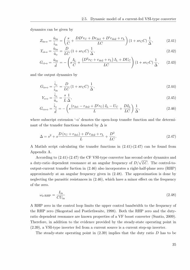
2.5. Dynamic model of a current-fed VSI-type converter
dynamics can be given by
Zin-o =uin
iin=
(s
C+
DD′rC +Drds1 +D′rds2 + rLLC
)
(1 + srCC)1
∆, (2.41)
Toi-o =uin
uo
=D
LC(1 + srCC)
1
∆, (2.42)
Gci-o =uin
d= −
(
sILC
+
(D2rC + rds2 + rL
)IL +DUC
LC
)
(1 + srCC)1
∆, (2.43)
and the output dynamics by
Gio-o =io
iin=
D
LC(1 + srCC)
1
∆, (2.44)
Yo-o =iouo
=s
L
1
∆, (2.45)
Gco-o =io
d= −
(
s(rds1 − rds2 +D′rC) IL − UC
L+
DILLC
)1
∆, (2.46)
where subscript extension ‘-o’ denotes the open-loop transfer function and the determi-
nant of the transfer functions denoted by ∆ is
∆ = s2 + sD (rC + rds1) +D′rds2 + rL
L+
D2
LC. (2.47)
A Matlab script calculating the transfer functions in (2.41)-(2.47) can be found from
Appendix A.
According to (2.41)-(2.47) the CF VSI-type converter has second order dynamics and
a duty-ratio dependent resonance at an angular frequency of D/√LC. The control-to-
output-current transfer fuction in (2.46) also incorporates a right-half-plane zero (RHP)
approximately at an angular frequency given in (2.48). The approximation is done by
neglecting the parasitic resistances in (2.46), which have a minor effect on the frequency
of the zero.
ωz-RHP =Iin
CUin
(2.48)
A RHP zero in the control loop limits the upper control bandwidth to the frequency of
the RHP zero (Skogestad and Postlethwaite, 1998). Both the RHP zero and the duty-
ratio dependent resonance are known properties of a VF boost converter (Suntio, 2009).
Therefore, in addition to the evidence provided by the steady-state operating point in
(2.39), a VSI-type inverter fed from a current source is a current step-up inverter.
The steady-state operating point in (2.39) implies that the duty ratio D has to be
35

Chapter 2. Dynamic modeling of photovoltaic converters
decreased in order to increase the output current or the input voltage. The frequency-
domain evidence of this phenomenon is the minus sign in front of the control-related
transfer functions in (2.43) and (2.46), which effectively means that their low-frequency
phase is 180. Therefore, if direct-duty-ratio-type control of the output current or the
input voltage is to be implemented, the reference has to be subtracted from the feedback
signal, which is an inversion of the typical practice in control engineering (Dorf and
Bishop, 2001).
2.5.1 Effect of photovoltaic generator
The source-affected H-parameters of the VSI-type converter are given in this section.
The symbolic transfer functions are calculated based on Fig. 2.4 and (2.19), the nominal
transfer functions given in (2.41)-(2.47) and the source admittance of the PVG (YS =
1/rpv). The effect of the parasitic resistances of the power-stage components is omitted
in order to emphasize the effect of the dynamic resistance of the PVG. A Matlab script
containing the calculation of the source-affected transfer functions also including the
parasitic resistances can be found in Appendix A. The resulting input dynamics can be
given by
ZSAin-o =
uin
iinS=
s
C
1
∆SA
, (2.49)
T SAoi-o =
uin
uo
=D
LC
1
∆SA
, (2.50)
GSAci-o =
uin
d= − Io
LC
(Uo
Io+ sL
)1
∆SA
, (2.51)
and the output dynamics by
GSAio-o =
io
iinS=
D
LC
1
∆SA
, (2.52)
Y SAo-o =
iouo
=1
L
(
s+YS
C
)1
∆SA
=1
L
(
s+1
rpvC
)1
∆SA
, (2.53)
GSAco-o =
io
d=
Uin
L
[
s− 1
C
(IinUin
− YS
)]1
∆SA
(2.54)
=Uin
L
[
s− 1
C
(1
Rpv
− 1
rpv
)]1
∆SA
, (2.55)
36

2.5. Dynamic model of a current-fed VSI-type converter
where the superscript ‘SA’ denotes the source-affected transfer function, Rpv = Upv/Ipv =
Uin/Iin and the determinant of the source-affected transfer functions ∆SA is given by
∆SA = s2 + sYS
C+
D2
LC≈ s2 + s
1
rpvC+
D2
LC. (2.56)
According to the source-affected determinant in (2.56), the dynamic resistance of the
PVG (rpv) will attenuate the internal resonant behavior of the converter. Damping factor
of the transfer functions (2.49)-(2.56) is low when rpv is high, i.e. in the constant current
region (CCR), and the PVG has little or practically no effect on the nominal transfer
functions. On the other hand, in the constant voltage region (CVR), rpv is low and it
effectively shunts the converter input capacitor and the transfer functions will show the
properties of the first order dynamics of a VF VSI (Nousiainen et al., 2011a).
The dynamic resistance of the PVG has significant effect on the nominal control-to-
output-current transfer function Gco-o given in (2.46). The source-affected Gco-o given in
(2.55) has an operating-point-dependent zero at an angular frequency given by
ωz-SA =1
C
(IinUin
− YS
)
=1
C
(1
Rpv
− 1
rpv
)
. (2.57)
Because the dynamic resistance rpv is high in the CCR, it has practically no effect on
(2.57) compared to the nominal zero in (2.48). At the MPP, rpv coincides with the static
resistance Rpv as discussed in Section 2.4, and therefore the zero in (2.57) is located at
the origin of the complex plane. In the CVR, the dynamic resistance is low compared
to the static resistance, and consequently the zero in (2.57) lies on the left half of the
complex plane (LHP). Accordingly, the zero in the source-affected control-to-output-
current transfer function GSAco shifts from the RHP to the LHP when the operating point
moves from the CCR to the CVR as shown in (2.58).
CVR: rpv < Rpv ⇒ ωz < 0 LHP-zero
MPP: rpv = Rpv ⇒ ωz = 0 Origin
CCR: rpv > Rpv ⇒ ωz > 0 RHP-zero
(2.58)
The operating points and the main parameters of a low-power VSI-type PV inverter
are defined in Table 2.1. Fig. 2.12 shows its soure-affected control-to-output current
transfer function at three operating points: one of the operating points lies in the CCR,
one in the CVR and one is at the MPP. The low-frequency phase in Fig. 2.12 confirms
the movement of the zero in (2.57) along the complex plane as defined in (2.58). It can be
deduced that high-bandwidth current controller is easy to be implemented in the CVR
applying conventional feedback control. However, when the operating moves to the MPP,
37

Chapter 2. Dynamic modeling of photovoltaic converters
Table 2.1: Main parameters of the VSI-type converter and the PVG used as a source.
Iin (A) Uin (V) Uo (V) rpv (Ω) L C fsw
CCR 1.01 12.2 8.0 360.0MPP 0.95 15.6 8.0 16.4 220 µH 2.2 mF 100 kHzCVR 0.71 17.4 8.0 4.0
100
101
102
103
104
−20
0
20
40
Mag
nit
ude
(dB
A)
100
101
102
103
104
−90
0
90
180
Phas
e (d
eg)
Frequency (Hz)
CCR
MPP
CVR
Fig. 2.12: Control-to-output-current transfer function GSAco-o.
such an output-current-control loop becomes marginally stable and instability occurs
when the operating point is in the CCR. An unstable current loop can be stabilized in
the CCR with the cascaded control scheme, where an input-voltage controller determines
the output-current reference. This means that input-side control has to be implemented
in order to transfer maximum power. The cascaded control scheme is a standard in
photovoltaic inverters, however, the origin of why it is needed is explicitly explained only
recently (Nousiainen et al., 2011b; Puukko et al., 2011). The stabilizing effect of the
input-voltage control will be discussed in detail later in this thesis.
The source-affected control-to-input-voltage transfer function GSAci-o at the three op-
erating points is shown in Fig. 2.13. The phase behavior of GSAci-o does not show sim-
ilar operating-point-dependent characteristics as GSAco-o. According to Fig. 2.13, direct-
duty-ratio control of the VSI-type converter would be easy to implement, however, the
output-current loop is a must in grid-connected inverters in order to guarantee high-
quality output current. The source-affected output admittance Y SAo-o in Fig. 2.14 shows
operating-point-dependent behavior. At high frequencies, the inductor L dominates the
output admittance. In the CCR, when rpv is high, the low-frequency behavior is de-
38

2.5. Dynamic model of a current-fed VSI-type converter
100
101
102
103
104
−20
0
20
40
Mag
nit
ude
(dB
V)
100
101
102
103
104
0
45
90
135
180
Phas
e (d
eg)
Frequency (Hz)
CCR
MPP
CVR
Fig. 2.13: Control-to-input-voltage transfer function GSAci-o.
100
101
102
103
104
−40
−20
0
20
Mag
nit
ude
(dB
S)
100
101
102
103
104
−90
−45
0
45
90
Phas
e (d
eg)
Frequency (Hz)
CCR
MPP
CVR
Fig. 2.14: Output admittance Y SAo-o .
termined by the input capacitor, whereas in the CV region, low rpv shunts the input
capacitor. When the impedance of a certain circuit is determined, voltage sources are
considered as short circuits and current sources as open circuits. Therefore, when the
output impedance of the VSI-type inverter is observed, the inverter input terminals con-
sist of the parallel connection of the input capacitor C and rpv. Therefore, when rpv = 0,
the input capacitor is shorted and it does not contribute to the output impedance.
It is not meaningful to plot the source-affected input impedance ZSAin-o or the source-
39

Chapter 2. Dynamic modeling of photovoltaic converters
100
101
102
103
104
−60
−40
−20
0
Mag
nit
ude
(dB
)
100
101
102
103
104
−180
−135
−90
−45
0
Phas
e (d
eg)
Frequency (Hz)
CCR
MPP
CVR
Fig. 2.15: Reverse voltage transfer ratio TSAoi-o.
affected forward current gain GSAio-o because the measurement of these transfer functions
would require summing of excitation current to the PVG photocurrent, which is not
explicitly available for such a use. The input impedance is, however, an important
transfer function, because it can be used to determine the stability of the PVG/inverter
interface based on the inverse minor-loop gain concept presented in Section 2.3. The
closed-loop input impedance will be inspected considering the stability criterion later in
this thesis. Fig. 2.15 shows the source-affected reverse voltage transfer ratio T SAoi-o. It
can be used to study the effect of grid voltage fluctuations, such as voltage spikes or
dips, to the inverter input voltage. Fig. 2.15 can also be used to depict the behavior of
the forward current gain Gio-o because according to (2.42) and (2.44) Toi-o = Gio-o and
according to (2.50) and (2.52) T SAoi-o = GSA
io-o.
2.5.2 Comparison of current-fed and voltage-fed VSI
As has been discussed earlier, the PVG has the properties of both current and voltage
sources. Therefore it might occur to a reader that a model of a VF converter could be
applicable. In this section, the transfer functions of a VF VSI are compared with the
transfer functions of the CF VSI derived in the previous section. A VF VSI-type inverter
is shown in Fig. 2.16. The power-stage in Fig. 2.16 is exactly the same as the power-
stage of the CF VSI-type inverter shown in Fig. 2.10, only the type of the input source is
changed. The Y-parameters in (2.6) are used to represent the converter in Fig. 2.16. The
Y-parameters can be derived based on the H-parameters by solving the input current iin
from the input dynamics in (2.8) yielding
40
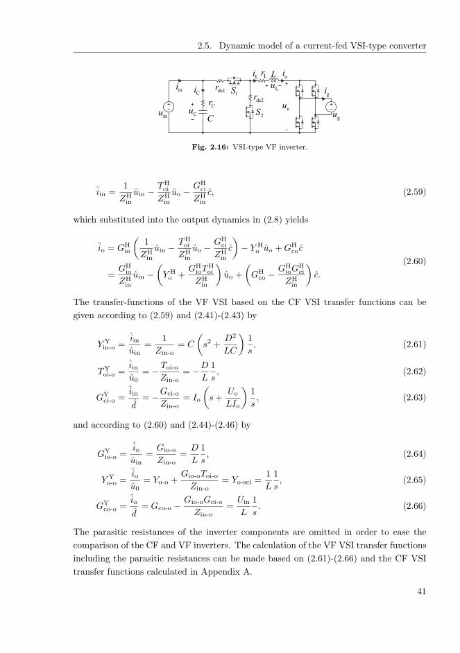
2.5. Dynamic model of a current-fed VSI-type converter
inuC
L oi
ou
gu
Li Lr
ds2rds1r
1S
2SCr
Cu
Ci giini Lu
Fig. 2.16: VSI-type VF inverter.
iin =1
ZHin
uin −THoi
ZHin
uo −GH
ci
ZHin
c, (2.59)
which substituted into the output dynamics in (2.8) yields
io = GHio
(1
ZHin
uin −THoi
ZHin
uo −GH
ci
ZHin
c
)
− Y Ho uo +GH
coc
=GH
io
ZHin
uin −(
Y Ho +
GHioT
Hoi
ZHin
)
uo +
(
GHco −
GHioG
Hci
ZHin
)
c.
(2.60)
The transfer-functions of the VF VSI based on the CF VSI transfer functions can be
given according to (2.59) and (2.41)-(2.43) by
Y Yin-o =
iinuin
=1
Zin-o
= C
(
s2 +D2
LC
)1
s, (2.61)
TYoi-o =
iinu0
= − Toi-o
Zin-o
= −D
L
1
s, (2.62)
GYci-o =
iin
d= −Gci-o
Zin-o
= Io
(
s+Uo
LIo
)1
s, (2.63)
and according to (2.60) and (2.44)-(2.46) by
GYio-o =
iouin
=Gio-o
Zin-o
=D
L
1
s, (2.64)
Y Yo-o =
iou0
= Yo-o +Gio-oToi-o
Zin-o
= Yo-sci =1
L
1
s, (2.65)
GYco-o =
io
d= Gco-o −
Gio-oGci-o
Zin-o
=Uin
L
1
s. (2.66)
The parasitic resistances of the inverter components are omitted in order to ease the
comparison of the CF and VF inverters. The calculation of the VF VSI transfer functions
including the parasitic resistances can be made based on (2.61)-(2.66) and the CF VSI
transfer functions calculated in Appendix A.
41

Chapter 2. Dynamic modeling of photovoltaic converters
100
101
102
103
104
−30
−20
−10
0
Mag
nit
ude
(dB
Ω)
100
101
102
103
104
−90
−45
0
45
Phas
e (d
eg)
Frequency (Hz)
CF
VF
Fig. 2.17: Input impedance Zin-o.
The output admittance of the VF VSI in (2.65) is the output admittance of the
CF VSI with short-circuited input given in (2.24), which is quite obvious because the
voltage source feeding the VSI in Fig. 2.16 is dynamically a short circuit, i.e. its internal
impedance is zero. The input impedance of both the CF and VF VSI is the same, because
according to (2.59) Y Yin = 1/ZH
in as shown in Fig. 2.17. When the input impedance
is observed from the input terminals, the source feeding the converter is dynamically
decoupled from the converter and thus does not short the input capacitor.
The output admittances of the CF and VF VSI are shown in Fig. 2.18. In the
VF VSI, the voltage source shorts the input capacitor and it does not influence the
output admittance as it does in the CF VSI. It can be concluded that the VF VSI
output admittance resembles the output admittance of a VSI-type PV inverter in the
CVR (Fig. 2.14), but as soon as the dynamic resistance of the PVG increases (i.e., the
operating point moves toward the MPP), the output impedance models derived with the
VF model can lead to false conclusions in the grid-interaction research. Therefore, the
type of input source has to be taken into account properly.
The control-to-output-current transfer functions are shown in Fig. 2.19. They follow
the similar behavior as the source affected Gco-o in Fig. 2.12. The VF converter control-
to-output-current transfer function has the properties of the PV inverter in the CVR,
i.e. it does not incorporate the RHP zero of the CF inverter. This means that the VF
inverter is a minimum-phase system compared to the non-minimum-phase dynamics of
the CF inverter. Although the VF inverter has some of the properties of the PV inverter
operating in the CVR, the VF model cannot be used to model the PV inverter because
42

2.6. Dynamic model of a current-fed semi-quadratic buck-boost converter
100
101
102
103
104
−40
−20
0
20
Mag
nit
ude
(dB
S)
100
101
102
103
104
−90
−45
0
45
90
Phas
e (d
eg)
Frequency (Hz)
CF
VF
Fig. 2.18: Output admittance Yo-o.
100
101
102
103
104
−20
0
20
40
Mag
nit
ude
(dB
A)
100
101
102
103
104
−90
0
90
180
Phas
e (d
eg)
Frequency (Hz)
CF
VF
Fig. 2.19: Control-to-output-current transfer function Gco-o.
it does not suffice for the input-voltage-controlled converter.
2.6 Dynamic model of a current-fed semi-quadratic buck-boost con-
verter
If the desired input voltage of a PV converter is less than the peak grid voltage, a
converter with buck-boost-type conversion ratio is needed. If the PVG in such a case is
composed of only a single PV module, the converter has to be capable of handling the wide
43

Chapter 2. Dynamic modeling of photovoltaic converters
iniinu
C1u1C
C3u 3C
L1uq1D
q2D
C1i
C3i
C2u2C
C2iL2i1L 2L
L2u
2S
1S
4S
3S
imuL3u
3LL3i oi
ou
L1i
Fig. 2.20: Current-fed semi-quadratic buck-boost converter.
conversion-ratio requirement. The current-fed semi-quadratic buck-boost (CFSQBB)
converter ([P4]-[P6]) proposed for modular transformerless PV applications is shown in
Fig. 2.20 with the defined components and polarities of the relevant currents and voltages.
The switches S1 and S4 can be equally substituted with diodes. The diodes Dq1 and
Dq2 with the inductor L2 and capacitor C2 form a quadratic element. The converter
integrates a quadratic current-step-down converter at the input side to handle the wide
conversion ratio and a current-step-up converter (i.e., the VSI-type converter) to handle
the grid-side controls. Cascaded with the unfolding full-bridge, the CFSQBB can be
used as a single-phase PV micro inverter. The placement of the capacitor C3 between
the positive terminals of the input and the intermediate voltages (uin, uim, respectively)
reduces the voltage stress of the capacitor by the amount of input voltage compared
to the conventional placement directly to the intermediate or dc-link terminals. The
CFSQBB converter may be controlled either in single- or dual-PWM mode depending
on the desired properties.
In the single-PWM mode, the on-time switches (S1 and S4) of the buck and boost
parts are controlled by the same duty ratio and the off-time switches (S2 and S3) by the
complement of the duty ratio. During the on-time, the switches S2 and S3 and the diode
Dq2 are off and the switches S1 and S4 and the diode Dq1 are conducting yielding the
on-time circuit structure given in Fig. 2.21. During the off-time, the switches S2 and
S3 and the diode Dq2 are conducting and the switches S1 and S4 and the diode Dq1
are off yielding the off-time circuit structure given in Fig. 2.22. Applying the averaging
teqhnique for the on- and off-time subcircuits, the average voltages across the inductors,
iniinu
C1u1C
C3u 3C
L1uC1i
C3i
C2u2C
C2iL2i1L 2L
L2u imuL3u
3LL3i oi
ou
L1i
Fig. 2.21: CFSQBB converter during on-time.
44

2.6. Dynamic model of a current-fed semi-quadratic buck-boost converter
iniinu
C1u1C
C3u 3C
L1uC1i
C3i
C2u2C
C2iL2i1L 2L
L2u imuL3u
3LL3i oi
ou
L1i
Fig. 2.22: CFSQBB converter during off-time.
the average currents through the capacitors as well as the average input voltage (uin),
intermediate voltage (uim) and output current (io) become as given in (2.67).
〈uL1〉 = 〈uC1〉 − 〈d〉 〈uC2〉 (2.67)
〈uL2〉 = 〈uC2〉 − 〈d〉 〈uC1〉 − 〈d〉 〈uC3〉 (2.68)
〈uL3〉 =(1− 〈d〉) 〈uC1〉+ (1− 〈d〉) 〈uC3〉 − 〈uo〉 (2.69)
〈iC1〉 = 〈iin〉 − 〈iL1〉+ 〈d〉 〈iL2〉 − (1− 〈d〉) 〈iL3〉 (2.70)
〈iC2〉 = 〈d〉 〈iL1〉 − 〈iL2〉 (2.71)
〈iC3〉 = 〈d〉 〈iL2〉 − (1− 〈d〉) 〈iL3〉 (2.72)
〈uim〉 = 〈uC1〉+ 〈uC3〉 (2.73)
〈uin〉 = 〈uC1〉 (2.74)
〈io〉 = 〈iL3〉 (2.75)
In order to maintain flux linkage and charge balances, the average voltages across the
inductors and average currents through the capacitors have to be zero. According to
these principles, the operating-point-related steady-state variables become with denoting
D′ = 1−D
IL1 = Iin, IL2 = DIin, IL3 =D2
D′Iin,
UC1 =D2
D′Uo, UC2 = (1 +D)Uo, UC3 =
D
D′Uo,
Uim =1
D′Uo, Uin =
D2
D′Uo, Io =
D2
D′Iin.
(2.76)
In the dual PWM mode, the duty ratios of the buck and boost switch pairs (S1, S3
and S2, S4, respectively) are controlled separately, allowing e.g. dedicated control systems
45

Chapter 2. Dynamic modeling of photovoltaic converters
iniinu
C1u1C
C3u 3C
L1uC1i
C3i
C2u2C
C2iL2i1L 2L
L2u imuL3u
3LL3i oi
ou
L1i
Fig. 2.23: CFSQBB converter during on-off-time.
iniinu
C1u1C
C3u 3C
L1uC1i
C3i
C2u2C
C2iL2i1L 2L
L2u imuL3u
3LL3i oi
ou
L1i
Fig. 2.24: CFSQBB converter during off-on-time.
for the output current and input voltage as well as separate control of the intermediate
voltage, which is the feasible control scheme of the single-phase modular inverter appli-
cation. Besides the on- and off-times, the dual-PWM operated circuit can exhibit two
extra states denoted by on-off- and off-on-times. During the on-off-time, the switches
S2 and S4 and the diode Dq2 are off and the switches S1 and S3 and the diode Dq1
are conducting yielding the on-off-time circuit structure given in Fig. 2.23. During the
off-on-time, the switches S2 and S4 and the diode Dq2 are conducting and the switches
S1 and S3 and the diode Dq1 are off yielding the off-on-time circuit structure given in
Fig. 2.24.
In order to solve the average voltages across the inductors, average currents through
the capacitors as well as average input voltage, intermediate voltage and output current,
synchronous PWM generation is assumed. The switching frequencies are assumed to
be equal as well as the beginning of the on-times of the buck and boost parts. The
synchronous PWM generation is realised by a digital control system. An extra state
appears between on- and off-times when d1 6= d2, where d1 and d2 are the duty ratios
of the buck- and boost-parts, respectively. If d1 > d2, the extra state is the on-off-time
and if d1 < d2, the extra state is the off-on-time. The average values can be solved by
common average integral, where Ts is the cycle time. For d1 < d2 we get the average
inductor voltages given by
〈uL1〉 =1
Ts
d1Ts∫
0
(uC1 − uC2) dt+
d2Ts∫
d1Ts
uC1dt+
Ts∫
d2Ts
uC1dt
,
〈uL2〉 =1
Ts
d1Ts∫
0
(uC2 − uC1 − uC3) dt+
d2Ts∫
d1Ts
uC2dt+
Ts∫
d2Ts
uC2dt
, (2.77)
46
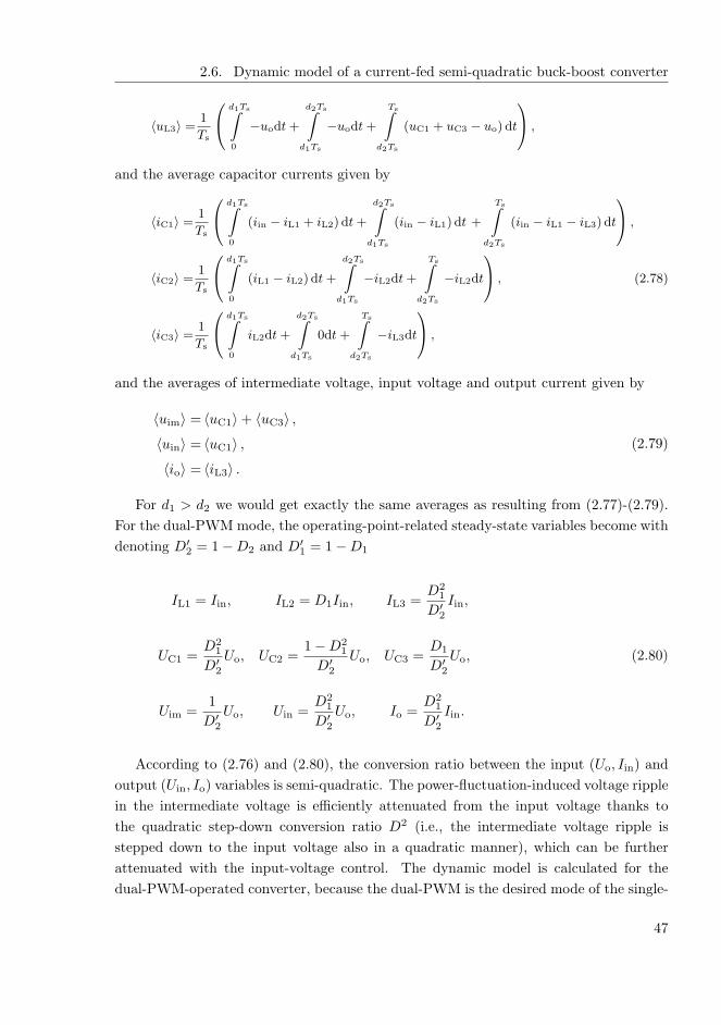
2.6. Dynamic model of a current-fed semi-quadratic buck-boost converter
〈uL3〉 =1
Ts
d1Ts∫
0
−uodt+
d2Ts∫
d1Ts
−uodt+
Ts∫
d2Ts
(uC1 + uC3 − uo) dt
,
and the average capacitor currents given by
〈iC1〉 =1
Ts
d1Ts∫
0
(iin − iL1 + iL2) dt+
d2Ts∫
d1Ts
(iin − iL1) dt +
Ts∫
d2Ts
(iin − iL1 − iL3) dt
,
〈iC2〉 =1
Ts
d1Ts∫
0
(iL1 − iL2) dt+
d2Ts∫
d1Ts
−iL2dt+
Ts∫
d2Ts
−iL2dt
, (2.78)
〈iC3〉 =1
Ts
d1Ts∫
0
iL2dt+
d2Ts∫
d1Ts
0dt+
Ts∫
d2Ts
−iL3dt
,
and the averages of intermediate voltage, input voltage and output current given by
〈uim〉 = 〈uC1〉+ 〈uC3〉 ,〈uin〉 = 〈uC1〉 ,〈io〉 = 〈iL3〉 .
(2.79)
For d1 > d2 we would get exactly the same averages as resulting from (2.77)-(2.79).
For the dual-PWM mode, the operating-point-related steady-state variables become with
denoting D′
2 = 1−D2 and D′
1 = 1−D1
IL1 = Iin, IL2 = D1Iin, IL3 =D2
1
D′
2
Iin,
UC1 =D2
1
D′
2
Uo, UC2 =1−D2
1
D′
2
Uo, UC3 =D1
D′
2
Uo,
Uim =1
D′
2
Uo, Uin =D2
1
D′
2
Uo, Io =D2
1
D′
2
Iin.
(2.80)
According to (2.76) and (2.80), the conversion ratio between the input (Uo, Iin) and
output (Uin, Io) variables is semi-quadratic. The power-fluctuation-induced voltage ripple
in the intermediate voltage is efficiently attenuated from the input voltage thanks to
the quadratic step-down conversion ratio D2 (i.e., the intermediate voltage ripple is
stepped down to the input voltage also in a quadratic manner), which can be further
attenuated with the input-voltage control. The dynamic model is calculated for the
dual-PWM-operated converter, because the dual-PWM is the desired mode of the single-
47

Chapter 2. Dynamic modeling of photovoltaic converters
phase inverter application. The computation of the average model including the parasitic
resistances can be carried out by substituting the subcircuit equations including the
parasitics into (2.77)-(2.79). Such averaging and the linearization of the average model is
space-consuming mechanical work, and therefore, we skip directly to the operating point
including the parasitic resistances, which can be given by
Uin −D1UC3 − IinrL1 +D21IinrC3 −D1IinrC3 = 0, (2.81)
UC3 −D1 (Uim + IinrL2)−D21Iin (rC1 + rC2 − rL2) = 0, (2.82)
D′22 Uim −D′
2
[D2
1Iin (rC1 + rC2) + Uo
]−D2
1IinrL3 = 0, (2.83)
and to the the linearized state-space given in (2.84). The merged resistances and voltages
in (2.84) are given in (2.85).
duC1
dt=−
1
C1
iL1 +D1
C1
iL2 −D′
2
C1
iL3 +1
C1
iin +D1Iin
C1
d1 +D2
1Iin
D′
2C1
d2
duC2
dt=D1
C2
iL2 −D′
2
C2
iL3 +D1Iin
C2
d1 +D2
1Iin
D′
2C2
d2
duC3
dt=D1
C3
iL1 −1
C3
iL2 +Iin
C3
d1
diL1
dt=
1
L1
uC1 −D1
L1
uC3 −R1
L1
iL1 +R2
L1
iL2 −rC1D
′
2
L1
iL3 +rC1
L1
iin −U1
L1
d1 +D2
1IinrC1
D′
2L1
d2
diL2
dt=−
D1
L2
uC1 −D1
L2
uC2 +1
L2
uC3 +R2
L2
iL1 −R3
L2
iL2 −D1rC1
L2
iin −U2
L2
d1
diL3
dt=D′
2
L3
uC1 +D′
2
L3
uC2 −rC1D
′
2
L3
iL1 −R4
L3
iL3 +rC1D
′
2
L3
iin −1
L3
uo −U3
L3
d2
uim =
(
1 + rC1C1
d
dt
)
uC1 +
(
1 + rC2C2
d
dt
)
uC2
uin =
(
1 + rC1C1
d
dt
)
uC1
io =iL3
(2.84)
R1 = rC1 + rL1 +D1rC3
R2 = D1 (rC1 + rC2)
R3 = rC3 + rL2 +D1 (rC1 + rC2 − rL2)
R4 = D′
2 (rC1 + rC2) + rL3
U1 = UC3 −D1Iin (rC1 + rC3) + IinrC3
U2 = Uim +D1Iin (rC1 + rC2 − rL2)− IinrC3
U3 = Uim −D21Iin (rC1 + rC2) /D
′
2
(2.85)
48

2.6. Dynamic model of a current-fed semi-quadratic buck-boost converter
The transfer-function set of the CFSQBB, given in (2.86) based on (2.84), has one
extra input and output variables compared to the regular H-parameters. The effect of
the non-ideal Norton equivalent source can be solved by substitutig iin = iinS − YSuin
into (2.86), which yields (2.87)-(2.98).
uim
uin
io
=
Zim-o Toim-o Gcim1-o Gcim2-o
Zin-o Toi-o Gci1-o Gci2-o
Gio-o −Yo-o Gco1-o Gco2-o
iin
uo
d1
d2
(2.86)
ZSAim-o =
uim
iinS=
Zim-o
1 + YSZin-o
(2.87)
TSAoim-o =
uim
uo
=
1 + YS
(
Zin-o −Toi-oZim-o
Toim-o
)
1 + YSZin-o
Toim-o (2.88)
GSAcim1-o =
uim
d1=
1 + YS
(
Zin-o −Gci1-oZim-o
Gcim1-o
)
1 + YSZin-o
Gcim1-o (2.89)
GSAcim2-o =
uim
d2=
1 + YS
(
Zin-o −Gci2-oZim-o
Gcim2-o
)
1 + YSZin-o
Gcim2-o (2.90)
ZSAin-o =
uin
iinS=
Zin-o
1 + YSZin-o
(2.91)
TSAoi-o =
uin
uo
=Toi-o
1 + YSZin-o
(2.92)
GSAci1-o =
uin
d1=
Gci1-o
1 + YSZin-o
(2.93)
GSAci2-o =
uin
d2=
Gci2-o
1 + YSZin-o
(2.94)
GSAio-o =
io
iinS=
Gio-o
1 + YSZin-o
(2.95)
YSAo-o =
io
uo
=
1 + YS
(
Zin-o +Toi-oGio-o
Yo-o
)
1 + YSZin-o
Yo-o (2.96)
GSAco1-o =
io
d1=
1 + YS
(
Zin-o −Gci1-oGio-o
Gco1-o
)
1 + YSZin-o
Gco1-o (2.97)
GSAco2-o =
io
d2=
1 + YS
(
Zin-o −Gci2-oGio-o
Gco2-o
)
1 + YSZin-o
Gco2-o (2.98)
49

Chapter 2. Dynamic modeling of photovoltaic converters
The dynamic properties of the CFSQBB converter will be discussed in more detail
in the next chapter, where its control-system design in the micro-inverter application is
studied. The calculation of both the source and non-source-affected open-loop transfer
functions of the CFSQBB is provided in Appendix B as a Matlab script.
50

3 CLOSED-LOOP FORMULATION &
CONTROL-SYSTEM DESIGN
This chapter presents the dynamic formulation of the input-voltage and output-current
controlled converters as well as the converter with the cascaded control scheme. Control-
system design examples are shown for the VSI-type PV inverter as well as for an inverter
based on the CFSQBB converter. The closed-loop analysis reveals the relation between
the input-voltage-control stability of the VSI with the cascaded control scheme and the
size of its input capacitor as well as the negative output impedance originating from
the multiplier-based grid synchronization. The theory is derived in the continuous-time
domain although the controllers are implemented with a microprocessor in the discrete-
time domain. The control delay imposed by the discrete implementation is taken into
account by Pade approximant of the time delay. The feasibility of such an analysis is
verified in the experimental measurements.
3.1 Input-voltage control
The control-block diagram of an input-voltage-controlled converter is shown in Fig. 3.1,
where Ga is the modulator gain, Gvc is the input-voltage controller transfer function, uuinref
is the input-voltage reference generated by the MPPT facility, Ginse is the input-voltage-
sensing gain and Rineq is the equivalent input-current-sensing resistor. The duty ratio d
can be given according to Fig. 3.1 by
d = GaGvc
(uuinref −Gin
seuin
). (3.1)
The closed-loop input voltage uin can be solved according to Fig. 3.1 yielding
uin =Zin-oiin + Toi-ouo +Gci-oGaGvc
(uuinref −Gin
seuin
)
=Zin-o
1 + Lin
iin +Toi-o
1 + Lin
uo +Lin
1 + Lin
1
Ginse
uinref,
(3.2)
where the input-voltage-control loop denoted by Lin is
Lin = GinseGvcGaGci-o. (3.3)
51

Chapter 3. Closed-loop formulation & control-system design
vcG
in
seG
ou
inu
oi
uin
refud
MPPTin
eqR
o-oY
io-oGOpen loop
co-oG
ini
ci-oG
oi-oT
in-oZ
Outputdynamics
Inputdynamics
aG
Fig. 3.1: Control-block diagram of the input-voltage-controlled converter.
The stability of the input-voltage control loop can be determined by applying the Nyquist
stability criterion to Lin.
The closed-loop output current io can be solved according to Fig. 3.1 yielding
io = Gio-oiin − Yo-ouo +Gco-oGaGvc
(uuinref −Gin
seuin
). (3.4)
Substituting (3.2) into (3.4) yields
io =
(Gio-o
1 + Lin
+Lin
1 + Lin
Gio-∞
)
iin −(
Yo-o
1 + Lin
+Lin
1 + Lin
Yo-∞
)
uo
+Lin
1 + Lin
Gco-o
Gci-o
1
Ginse
uinref,
(3.5)
where the ideal forward current gain Gio-∞ is given in (3.6) and the ideal output admit-
tance Yo-∞ was given earlier in (2.25).
Gio-∞ = Gio-o −Zin-oGco-o
Gci-o
(3.6)
The input-dynamics of the input-voltage controlled converter can be summarized accord-
ing to (3.2) by
Z inin-c =
uin
iin=
Zin-o
1 + Lin
, (3.7)
52
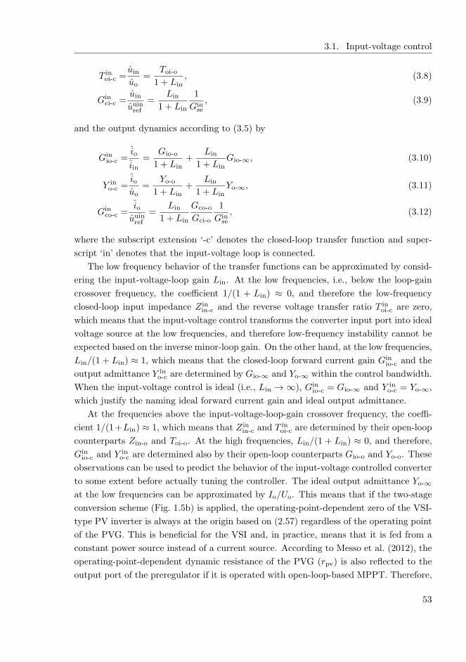
3.1. Input-voltage control
T inoi-c =
uin
uo
=Toi-o
1 + Lin
, (3.8)
Ginci-c =
uin
uuinref
=Lin
1 + Lin
1
Ginse
, (3.9)
and the output dynamics according to (3.5) by
Ginio-c =
io
iin=
Gio-o
1 + Lin
+Lin
1 + Lin
Gio-∞, (3.10)
Y ino-c =
iouo
=Yo-o
1 + Lin
+Lin
1 + Lin
Yo-∞, (3.11)
Ginco-c =
iouuinref
=Lin
1 + Lin
Gco-o
Gci-o
1
Ginse
, (3.12)
where the subscript extension ‘-c’ denotes the closed-loop transfer function and super-
script ‘in’ denotes that the input-voltage loop is connected.
The low frequency behavior of the transfer functions can be approximated by consid-
ering the input-voltage-loop gain Lin. At the low frequencies, i.e., below the loop-gain
crossover frequency, the coefficient 1/(1 + Lin) ≈ 0, and therefore the low-frequency
closed-loop input impedance Z inin-c and the reverse voltage transfer ratio T in
oi-c are zero,
which means that the input-voltage control transforms the converter input port into ideal
voltage source at the low frequencies, and therefore low-frequency instability cannot be
expected based on the inverse minor-loop gain. On the other hand, at the low frequencies,
Lin/(1 + Lin) ≈ 1, which means that the closed-loop forward current gain Ginio-c and the
output admittance Y ino-c are determined by Gio-∞ and Yo-∞ within the control bandwidth.
When the input-voltage control is ideal (i.e., Lin → ∞), Ginio-c = Gio-∞ and Y in
o-c = Yo-∞,
which justify the naming ideal forward current gain and ideal output admittance.
At the frequencies above the input-voltage-loop-gain crossover frequency, the coeffi-
cient 1/(1+Lin) ≈ 1, which means that Z inin-c and T in
oi-c are determined by their open-loop
counterparts Zin-o and Toi-o. At the high frequencies, Lin/(1 + Lin) ≈ 0, and therefore,
Ginio-c and Y in
o-c are determined also by their open-loop counterparts Gio-o and Yo-o. These
observations can be used to predict the behavior of the input-voltage controlled converter
to some extent before actually tuning the controller. The ideal output admittance Yo-∞
at the low frequencies can be approximated by Io/Uo. This means that if the two-stage
conversion scheme (Fig. 1.5b) is applied, the operating-point-dependent zero of the VSI-
type PV inverter is always at the origin based on (2.57) regardless of the operating point
of the PVG. This is beneficial for the VSI and, in practice, means that it is fed from a
constant power source instead of a current source. According to Messo et al. (2012), the
operating-point-dependent dynamic resistance of the PVG (rpv) is also reflected to the
output port of the preregulator if it is operated with open-loop-based MPPT. Therefore,
53

Chapter 3. Closed-loop formulation & control-system design
in such a case, the inverter control dynamics contain a zero that may be located both at
the RHP or LHP depending on the operating point of the PVG. Consequently, the input-
voltage control is a highly recommended practice for the preregulator in the two-stage
conversion scheme.
3.2 Output-current control
The first step of the procedure to solve the output-controlled-converter dynamics is the
linearization of the duty ratio due to the multiplier-based synchronization (Fig. 1.5a
and Fig. 1.5b). The output-current reference is shaped according to the output voltage
waveform in order to inject current at near unity power factor to the grid without the need
for more complex phase-locked-loop-based (PLL) synchronization methods (Blaabjerg
et al., 2006). The duty ratio in the time-domain can be given by
d = GaGcc
(Gout
se uouioref −Rout
eq io), (3.13)
and in the frequency domain by
d = GaGcc
(
Goutse Uou
ioref +Gout
se U iorefuo −Rout
eq io
)
, (3.14)
where the elements either in the time or frequency domain are defined as follows: Gcc is
the current controller, Goutse output-voltage-sensing function, Rout
eq the equivalent output-
current-sensing resistor and uioref the current-reference voltage signal. According to (3.14),
the control-block diagram of the output-current controlled converter can be presented as
shown in Fig. 3.2.
The closed-loop output current can be solved from Fig. 3.2 yielding
io =Gio-oiin − Yo-ouo +Gco-oGaGcc
(
Goutse Uou
ioref +Gout
se U iorefuo −Rout
eq io
)
=Gio-o
1 + Lout
iin −(
Yo-o
1 + Lout
− Lout
1 + Lout
Yff
)
uo +1
Routeq
Lout
1 + Lout
uioref,
(3.15)
where the output-current-loop gain Lout is given in (3.16), the feedforward admittance Yff
originating from the grid synchronization is given in (3.17) and the steady-state current
reference U ioref in (3.17) is given in (3.18). Applying the Nyquist stability criterion to the
output-current-loop gain Lout determines the stability of the output-current control.
Lout =Routeq GccGaGco-o (3.16)
Yff =1
Routeq
Goutse U io
ref (3.17)
54

3.2. Output-current control
ccG
out
se oG Uout io
se refG U
out
eqR
ou
inu
oi
d
io
refuaG
o-oY
io-oGOpen-loop
co-oG
ini
ci-oG
oi-oT
in-oZ
Outputdynamics
Inputdynamics
Effect of synchronization
Fig. 3.2: Control-block diagram of the output-current-controlled converter.
U ioref =
IoRouteq (s = 0)
UoGoutse (s = 0)
(3.18)
The closed-loop input voltage can be solved according to Fig. 3.2 by
uin = Zin-oiin + Toi-ouo +Gci-oGaGcc
(
Goutse Uou
ioref +Gout
se Vcuo −Routeq io
)
. (3.19)
Substituting (3.15) into (3.19) yields
uin =
(Zin-o
1 + Lout
+Lout
1 + Lout
Zin-∞
)
iin
+
[Toi-o
1 + Lout
+Lout
1 + Lout
(
Toi-∞ +Gci
Gco
Yff
)]
uo
+1
Routeq
Lout
1 + Lout
Gci
Gco
Goutse Uou
ioref,
(3.20)
where the ideal reverse voltage transfer ratio Toi-∞ is defined in (3.21) and the ideal input
impedance Zin-∞ was defined earlier in (2.17).
Toi-∞ = Toi-o +Gci-oYo-o
Gco-o
(3.21)
The input dynamics of the output-current-controlled converter can be summarized ac-
55

Chapter 3. Closed-loop formulation & control-system design
cording to (3.20) by
Zoutin-c =
uin
iin=
Zin-o
1 + Lout
+Lout
1 + Lout
Zin-∞, (3.22)
T outoi-c =
uin
uo
=Toi-o
1 + Lout
+Lout
1 + Lout
(
Toi-∞ +Gci-o
Gco-o
Yff
)
, (3.23)
Goutci-c =
uin
uioref
=1
Routeq
Lout
1 + Lout
Gci
Gco
Goutse Uo, (3.24)
and output dynamics according to (3.15) by
Goutio-c =
io
iin=
Gio-o
1 + Lout
, (3.25)
Y outo-c =
iouo
=Yo-o
1 + Lout
− Lout
1 + Lout
Yff, (3.26)
Goutco-c =
iouioref
=1
Routeq
Lout
1 + Lout
, (3.27)
where the superscript ‘out’ denotes that the output-current-control loop is connected.
The transfer function Goutci-c in (3.24) between the output-current reference and the in-
put voltage determines the properties of the input-voltage control in the cascaded control
scheme. It can be seen that the original control-to-output-current transfer function Gco-o
in (3.24) is located in the denominator, which means that the operating point dependent
zero of Gco-o in (2.57) introduces a pole to Goutci-c, which may locate in the RHP and is
one of the explanations why the CF VSI with mere output-current control is unstable.
Another explanation is the input impedance of the output-current-controlled converter
Zoutin-c given in (3.22). The behavior of Zout
in-c at the frequencies below the current-loop-
gain crossover frequency is determined by Zin-∞, which can be approximated by −Uin/Iin
at the named frequencies. At the MPP, Uin/Iin equals the low-frequency value of the
PVG impedance (rpv) with a negative sign, and therefore the output-current-controlled
converter becomes unstable at the MPP owing to the minor-loop gain instability. This
condition is valid also for the output-voltage-controlled PV converter (Leppaaho et al.,
2010), which implies that mere output-side control of a PV converter cannot be used for
maximum power transfer.
According to (3.26), the output admittance Y outo-c of the output-current-controlled
converter is determined by the feedforward admittance Yff with a negative sign up to
the current-loop-crossover frequency. Therefore, the inverter output impedance 1/Y outo-c
has negative-incremental-resistor-like behavior at those frequencies. It can be seen from
(3.26), that if Yff = 0, the low-frequency behavior of the output admittance resembles
ideal current source, i.e. the low-frequency admittance is zero. Consequently, it can
56

3.3. Cascaded control scheme
be deduced that grid synchronization can impair the current-source property of a grid-
connected inverter.
3.3 Cascaded control scheme
In the cascaded control scheme, the MPPT facility generates the input-voltage reference
which is subtracted from the input-voltage-feedback signal because the control signal, i.e.
the output current reference, has to be increased in order to decrease to input voltage.
The input-voltage-error signal is then fed to the input voltage controller, whose output is
used as the control variable for the output-current-controlled converter in Fig. 3.2. The
control-block diagram of the cascaded control scheme can be given according to the trans-
fer functions (3.22)-(3.27) as shown in Fig. 3.3, where Ginvc denotes the input-voltage con-
troller, Ginse the input-voltage-sensing gain and Rin
eq the equivalent input-current-sensing
resistor.
According to Fig. 3.3, the output-current reference uioref can be given by
uioref = Gin
vc
(Gin
seuin − uuinref
), (3.28)
in
vcG
in
seG
ou
inu
oi
uin
refu
io
refu
MPPTin
eqR
out
o-cY
out
io-cG
Output-current-controlledconverter
out
co-cG
ini
out
ci-cG
out
oi-cT
out
in-cZ
Outputdynamics
Inputdynamics
Fig. 3.3: Control-block diagram of the cascaded control scheme.
57

Chapter 3. Closed-loop formulation & control-system design
and the closed-loop input voltage can be solved by
uin =Zoutin-ciin + T out
oi-c uo +Goutci-cG
invc
(Gin
seuin − uuinref
)
=Zoutin-c
1− Lin
iin +T outoi-c
1− Lin
uo +1
Ginse
Lin
1− Lin
uuinref ,
(3.29)
where the input-voltage-control loop gain Lin, which determines the input-voltage-control
stability, is defined as
Lin = GinseG
invcG
outci-c. (3.30)
The closed-loop output current can be given according to Fig. 3.3 by
io = Goutio-ciin − Y out
o-c uo +Goutco-cG
invc
(Gin
seuin − uuinref
). (3.31)
Substituting (3.29) into (3.31) yields
io =
(Gout
io-c
1− Lin
− Lin
1− Lin
Goutio-∞
)
iin −(
Y outo-c
1− Lin
− Lin
1− Lin
Y outo-∞
)
uo
− 1
Ginse
Lin
1− Lin
Goutco-c
Goutci-c
uuinref ,
(3.32)
where
Goutio-∞ =Gout
io-c −Zoutin-cG
outco-c
Goutci-c
, (3.33)
Y outo-∞ =Y out
o-c +T outoi-vG
outco-c
Goutci-c
. (3.34)
The closed-loop input dynamics of the converter under the cascaded control scheme
can be summarized according to (3.29) as given in (3.35)-(3.37). Substituting the output-
current-controlled-converter transfer functions (3.22)-(3.24) into (3.35)-(3.37) yields the
closed-loop transfer functions given by the original open-loop trasfer functions as defined
in (3.38)-(3.40)
Zout-inin-c =
uin
iin=
Zoutin-c
1− Lin
(3.35)
T out-inoi-c =
uin
uo
=T outoi-c
1− Lin
(3.36)
Gout-inci-c =
uin
uuinref
=1
Ginse
Lin
1− Lin
(3.37)
58

3.4. Control-system design
Zout-inin-c =
Zin-o
(1 + Lout) (1− Lin)+
Lout
(1 + Lout) (1− Lin)Zin-∞ (3.38)
T out-inoi-c =
Toi-o
(1 + Lout) (1− Lin)+
Lout
(1 + Lout) (1− Lin)
(
Toi-∞ +Gci-o
Gco-o
Yff
)
(3.39)
Gout-inci-c =
1
Ginse
Lin
1− Lin
(3.40)
The closed-loop output dynamics of the converter under the cascaded control scheme
can be summarized according to (3.32) as given in (3.41)-(3.43), and the substitution of
the output-current-controlled converter output dynamics from (3.25)-(3.27) into (3.41)-
(3.43) yields (3.44)-(3.46).
Gout-inio-c =
io
iin=
Goutio-c
1− Lin
− Lin
1− Lin
Goutio-∞ (3.41)
Y out-ino-c =
iouo
=Y outo-c
1− Lin
− Lin
1− Lin
Y outo-∞ (3.42)
Gout-inco-c =
iouuinref
= − 1
Ginse
Lin
1− Lin
Goutco-c
Goutci-c
(3.43)
Gout-inio-c =
Gio-o
(1 + Lout) (1− Lin)− Lin
1− Lin
Gio-∞ (3.44)
Y out-ino-c =
Yo-o
(1 + Lout) (1− Lin)− Lin
1− Lin
Yo-∞ − Lout
(1 + Lout) (1− Lin)Yff (3.45)
Gout-inco-c = − 1
Ginse
Lin
1− Lin
Gco-o
Gci-o
(3.46)
The closed-loop output admittance Y out-ino-c in (3.45) shows that at the frequencies
lower than the input-voltage-loop-gain crossover frequency, the input-voltage loop gain
Lin attenuates the feedforward-admittance (Yff) term, and the low-frequency behavior
of the output admittance is determined by Yo-∞. This is beneficial for the utility grid
because in case of the cascaded control scheme, the negative-resistor-like behavior of
the inverter output impedance is located between the crossover frequencies of the input-
voltage and output-current loops, whereas in output-current-controlled converter such
behavior also dominates at the low frequencies.
3.4 Control-system design
In this section, control-system-design examples are shown for the VSI and CFSQBB-type
inverters. The controllers are designed in the continuous time domain by utilizing typical
loop-shaping techniques. The continuous controllers are transformed into the discrete
59

Chapter 3. Closed-loop formulation & control-system design
time domain by bilinear transformation for the practical utilization in a microprocessor-
based control system (Franklin et al., 1998).
3.4.1 VSI-type inverter
The VSI-type PV inverter is shown in Fig. 3.4 with its control system. The sensing
functions are first-order low-pass filters with the cut-off frequency tuned at half the
switching frequency. The low-frequency gain of the equvalent input and output-current-
sensing resistors Rineq and Rout
eq as well as the input-voltage-sensing gain Ginse is set to
unity. The low-frequency gain of the output-voltage-sensing gain Goutse is set to 1/Uo.
The modulator gain Ga is also set to unity. In addition, it includes the processing
delay of the discrete control-system implementation by second-order Pade approximation,
which only affects the phase behavior of Ga, starting from approximately decade lower
than the sampling frequency. The sampling frequency used in this thesis is the same as
the switching frequency of the converter. The calculation of the numerical closed-loop
transfer functions is provided in Appendix C as a Matlab script.
The current-controller design is based on the output-current loop Lout given in (3.16),
where the main contributor is the control-to-output-current transfer function Gco-o.
The source-affected control-to-output-current transfer function GSAco-o incorporates the
operating-point-dependent zero given in (2.57) that is located on the RHP in the CCR
and on the LHP in the CVR. At the MPP, the zero is located at the origin as was shown
earlier in Fig. 2.12.
If the output-current-controlled converter is designed to operate in the CCR in a
stable manner, the control bandwidth of the current loop is, in practice, limited by the
RHP-zero frequency. In a typical single-phase inverter, the RHP-zero frequency is in the
order of a few tens of Hz at maximum. Such low-bandwidth output-current controller
has no practical usage but will work as demonstrated in (Nousiainen et al., 2011a). A
ccGMPPT
inuC
L oi
ou
gi
gu
ini
vcG
in
eq inR iin
se inG u
uin
refu out
se oG u
out
eq oR i
d
io
refu
aG
d ¢
Fig. 3.4: VSI-type inverter and its control system.
60

3.4. Control-system design
high-bandwidth current loop can be easily designed in the CVR because the zero of
GSAco-o lies in the LHP and the converter dynamics resemble the first-order dynamics of
the VSI fed by a voltage source. However, the converter becomes unstable with the
high-bandwidth current loop when the operating point reaches the MPP or enters into
the CCR as discussed earlier.
An output-current loop with a 4 kHz control bandwidth was designed in the CVR
based on a conventional PI-type controller with an additional high-frequency pole as
defined in (3.47), where kcc = 0.4, ωz-cc = 2π500 Hz and ωp-cc = 2π50 kHz.
Gcc = kccs+ ωz-cc
s
(s
ωp-cc
+ 1
) , (3.47)
The high-frequency pole ωp-cc was set to half the switching frequency in order to filter
out high-frequency noise. The pole cannot be located at too low a frequency with respect
to the bandwidth goal in order to not affect the phase margin (PM). The zero ωz-cc is
located at sufficiently high frequency in order to provide high low-frequency gain, but
also the effect of the zero on the PM has to be considered, which limits its frequency. The
gain kcc sets the desired crossover frequency of the loop. The predicted source-affected
output-current-loop gains are shown in Fig. 3.5 indicating that the phase (PM) and gain
(GM) margins of the current loop are 60 and 11 dB, respectively. In terms of operating
point, the loop gain clearly behaves as discussed above.
The dynamic properties of the input-voltage control are determined by the input-
100
101
102
103
104
−40
−20
0
20
40
60
Mag
nit
ud
e (d
B)
GMCVR
= 11 dB
100
101
102
103
104
−270
−180
−90
0
90
Phas
e (d
eg)
Frequency (Hz)
PMCVR
= 60°
CCR
MPP
CVR
Fig. 3.5: Output-current-loop gain Lout.
61

Chapter 3. Closed-loop formulation & control-system design
100
101
102
103
104
−40
−20
0
20
40
Mag
nit
ude
(dB
)
100
101
102
103
104
−90
0
90
180
Phas
e (d
eg)
Frequency (Hz)
CCR
MPP
CVR
Fig. 3.6: Control-to-input-voltage transfer function of the output-current-controlled converter(Gout-SA
ci-c ).
voltage-loop gain Lin, where the main contributor is the transfer function Goutci-c, given in
(3.37), from the output-current reference to the input voltage. The source-affected Goutci-c
is shown in Fig. 3.6. The low-frequency phase of Gout-SAci-c in Fig. 3.6 at the MPP is 90
due to a pole at the origin. The phase is 180 in the CVR due to a LHP pole and zero
in the CCR due to a RHP pole. This can be explained by substituting the associated
source-affected transfer functions without parasitic resistances into Goutci-c yielding (3.48).
Gout-SAci-c =
1
Routeq
Lout
1 + Lout
− 1
LC(Uo + IoLs)
Uin
L
[
s− 1
C
(1
Rpv
− 1
rpv
)]Goutse Uo. (3.48)
Eq. (3.48) shows that the zero of the source-affected control-to-output-current transfer
function GSAco-o in (2.57) is transformed into a pole in the input-voltage loop when the
bandwidth of the output-current loop is high (i.e. Lout/(1+Lout) ≈ 1). In case of a RHP
pole (i.e. the converter operates in the CCR), the bandwidth of the input-voltage loop
has to be higher than the RHP-pole frequency for stable operation with a reasonable
performance (Skogestad and Postlethwaite, 1998). Various papers discussing the input-
voltage control of a PV inverter do not recognize the existence of the RHP pole (Kadri
et al., 2011; Villanueva et al., 2009; Yazdani and Dash, 2009).
The input-voltage-control bandwidth of a single-phase inverter, on the other hand, is
limited because of the power-fluctuation-induced input-voltage ripple at twice the grid
62

3.4. Control-system design
frequency. The ripple voltage passing the input-voltage controller will pollute the grid-
current reference with the second harmonic component. Therefore, sufficient attenuation
is needed at the named frequency. In practice, the input-voltage-control bandwidth of
a single-phase inverter is typically limited to a few tens of Hertz. This implies that the
allowable input-voltage-control bandwidth has a certain range between the RHP pole
and the ripple frequencies. Therefore, the RHP pole, which is inversely proportional to
the input capacitance, has to be located at a sufficiently low frequency. Later in this
chapter this observation is used to derive a rule for minimum input capacitance.
Due to the minimum-bandwidth requirement of the input-voltage control, the worst-
case operating point in terms of the input-voltage control can be defined to be the point
where the PV current is the highest and the PV voltage is the lowest, because then
the RHP-pole frequency is the highest. The input-voltage controller of the inverter was
designed in the CCR by using the PI-type controller defined in (3.49), where kvc = 0.4,
ωz-vc = 2π4 Hz and ωp-vc = 2π75 Hz. The pole and zero of the voltage controller are
located in a similar manner as the pole and zero of the current controller.
Gvc = kvcs+ ωz-vc
s
(s
ωp-vc
+ 1
) , (3.49)
The predicted input-voltage loop gains at the three operating points are shown in
Fig. 3.7. Minimum PM of 49 is obtained with a crossover frequency of 22 Hz. It can be
deduced that the PM is always positive at voltages higher than the MPP voltage. The
100
101
102
103
104
−80
−40
0
40
Mag
nit
ude
(dB
)
100
101
102
103
104
−90
−45
0
45
90
135
Phas
e (d
eg)
Frequency (Hz)
PMmin
= 49°
CCR
MPP
CVR
Fig. 3.7: Input-voltage-loop gain Lin.
63
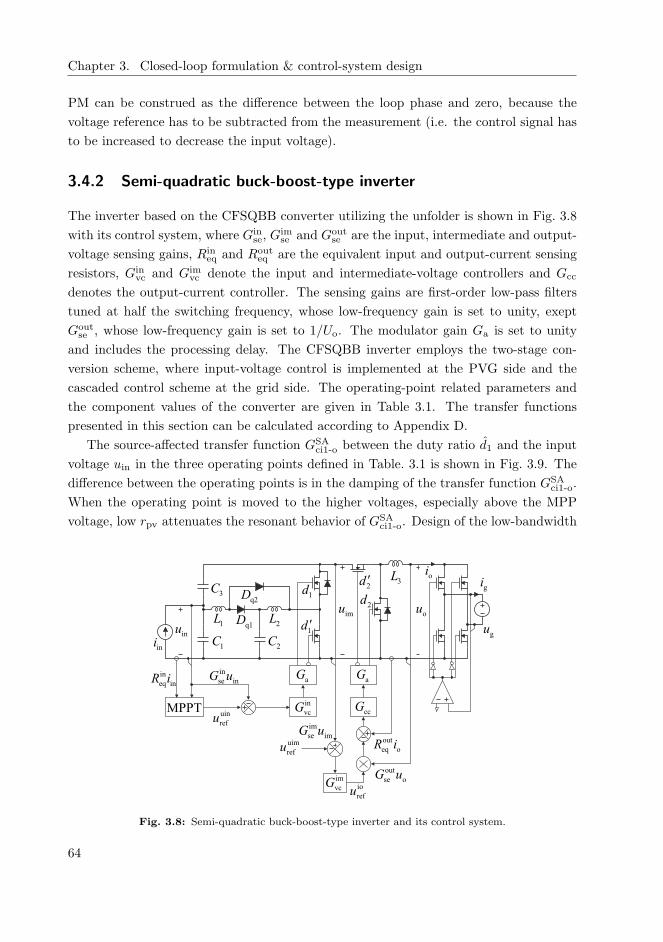
Chapter 3. Closed-loop formulation & control-system design
PM can be construed as the difference between the loop phase and zero, because the
voltage reference has to be subtracted from the measurement (i.e. the control signal has
to be increased to decrease the input voltage).
3.4.2 Semi-quadratic buck-boost-type inverter
The inverter based on the CFSQBB converter utilizing the unfolder is shown in Fig. 3.8
with its control system, where Ginse, G
imse and Gout
se are the input, intermediate and output-
voltage sensing gains, Rineq and Rout
eq are the equivalent input and output-current sensing
resistors, Ginvc and Gim
vc denote the input and intermediate-voltage controllers and Gcc
denotes the output-current controller. The sensing gains are first-order low-pass filters
tuned at half the switching frequency, whose low-frequency gain is set to unity, exept
Goutse , whose low-frequency gain is set to 1/Uo. The modulator gain Ga is set to unity
and includes the processing delay. The CFSQBB inverter employs the two-stage con-
version scheme, where input-voltage control is implemented at the PVG side and the
cascaded control scheme at the grid side. The operating-point related parameters and
the component values of the converter are given in Table 3.1. The transfer functions
presented in this section can be calculated according to Appendix D.
The source-affected transfer function GSAci1-o between the duty ratio d1 and the input
voltage uin in the three operating points defined in Table. 3.1 is shown in Fig. 3.9. The
difference between the operating points is in the damping of the transfer function GSAci1-o.
When the operating point is moved to the higher voltages, especially above the MPP
voltage, low rpv attenuates the resonant behavior of GSAci1-o. Design of the low-bandwidth
iniinu
1C
3C
q1D
q2D
2C
1L 2Limu
3L oi
ou
MPPTin
vcG ccG
im
vcG
gi
gu
out
eq oR iuim
refu
uin
refu
in
se inG uin
eq inR i
im
se imG u
1d2d
io
refu
out
se oG u
aG aG
1d ¢
2d ¢
Fig. 3.8: Semi-quadratic buck-boost-type inverter and its control system.
64

3.4. Control-system design
Table 3.1: Operating-point parameters of the CFSQBB inverter.
Iin (A) Uin (V) Uim (V) Uo (V) rpv (Ω) fsw (kHz)
CCR 7.84 15.0 370 230 56.0MPP 7.33 25.9 370 230 3.5 150CVR 5.70 29.0 370 230 0.8
C1 (µF) L1 (µH) C2 (µF) L2 (µH) C3 (µF) L3 (µH)20 220 20 1000 660 1000
100
101
102
103
104
0
20
40
60
Mag
nit
ude
(dB
V)
100
101
102
103
104
−180
−135
−90
−45
0
Phas
e (d
eg)
Frequency (Hz)
CCR
MPP
CVR
Fig. 3.9: Control-to-input-voltage transfer function GSAci1-o.
integral-type (I) input-voltage controller defined in (3.50) is a straightforward task. The
controller gain kin = 1.2 is selected to keep the peaking of the resonance in the input-
voltage loop Lin = GinseG
invcGaG
SAci1-o at approximately 1 kHz well below the 0 dB line
as shown in Fig. 3.10, which shows the input-voltage-loop gain in the three different
operating points. The resulting minimum phase and gain margins of the input-voltage-
control loop according to Fig. 3.10 are 12 dB and 86, respectively.
Ginvc =
kins
(3.50)
The transfer function between the output current io and the duty ratio d2 when the
input-side control is at open loop (Gco2-o) is shown in Fig. 3.11 with the source effect,
whereas Fig. 3.12 shows the same transfer function when the input-side control is at
closed loop (Ginco2-c), which can be solved by substituting the duty ratio d1, which can
be solved from Fig. 3.8, into the open-loop transfer function set of the CFSQBB given
65

Chapter 3. Closed-loop formulation & control-system design
100
101
102
103
104
−120
−80
−40
0
40
Mag
nit
ude
(dB
)
100
101
102
103
104
−360
−270
−180
−90
0
Phas
e (d
eg)
Frequency (Hz)
CCR
MPP
CVR
86°
12 dB
Fig. 3.10: Input-voltage-loop gain Lin.
10−1
100
101
102
103
104
−20
0
20
40
60
Mag
nit
ude
(dB
A)
10−1
100
101
102
103
104
−270
−180
−90
0
Phas
e (d
eg)
Frequency (Hz)
CCR
MPP
CVR
Fig. 3.11: Control-to-output-current transfer function GSAco2-o.
in (2.86). According to Nousiainen and Suntio (2011), Ginco2-c can be given as shown in
(3.51), where the superscript ‘in’ denotes that the input-voltage-control loop is connected.
Ginco2-c = Gco2-o −
Lin
1 + Lin
Gco1-oGci2-o
Gci1-o
. (3.51)
Fig. 3.11 shows that the output-current-control loop has similar operating-point-
dependent zero as the VSI-type PV inverter that shifts between the left and right halves
66

3.4. Control-system design
of the complex plane when the CFSQBB operates at open loop. Fig. 3.12 shows that the
input-voltage control shifts the zero very close to the origin regardless of the operating
point as discussed earlier, which simplifies the design of the cascaded control loop. The
output-current-loop gains Lout = Routeq GccGaG
inco2-c are shown in Fig. 3.13. The PI-type
output-current controller is shown in (3.52), where kcc = 0.05, ωz-cc = 2π50 kHz and
ωp-cc = 2π1 kHz. The stability of Lout is determined by the location of the aforemen-
tioned zero, which still may locate either on the RHP or the LHP depending on e.g.
100
101
102
103
104
0
20
40
60
Mag
nit
ude
(dB
A)
100
101
102
103
104
−270
−225
−180
−135
−90
Phas
e (d
eg)
Frequency (Hz)
CCR
MPP
CVR
Fig. 3.12: Control-to-output-current transfer function Gin-SAco2-c when the input-voltage loop is connected.
100
101
102
103
104
−40
−20
0
20
40
60
Mag
nit
ude
(dB
)
100
101
102
103
104
−180
−90
0
90
180
Phas
e (d
eg)
Frequency (Hz)
CCR
MPP
CVR
61°
16 dB
Fig. 3.13: Output-current-loop gain Lout.
67
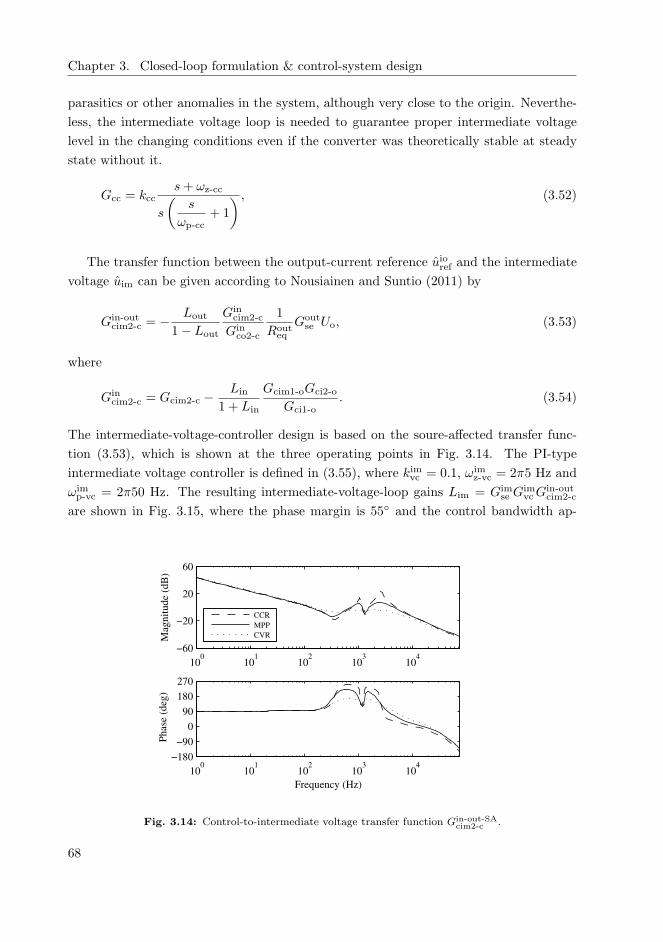
Chapter 3. Closed-loop formulation & control-system design
parasitics or other anomalies in the system, although very close to the origin. Neverthe-
less, the intermediate voltage loop is needed to guarantee proper intermediate voltage
level in the changing conditions even if the converter was theoretically stable at steady
state without it.
Gcc = kccs+ ωz-cc
s
(s
ωp-cc
+ 1
) , (3.52)
The transfer function between the output-current reference uioref and the intermediate
voltage uim can be given according to Nousiainen and Suntio (2011) by
Gin-outcim2-c = − Lout
1− Lout
Gincim2-c
Ginco2-c
1
Routeq
Goutse Uo, (3.53)
where
Gincim2-c = Gcim2-c −
Lin
1 + Lin
Gcim1-oGci2-o
Gci1-o
. (3.54)
The intermediate-voltage-controller design is based on the soure-affected transfer func-
tion (3.53), which is shown at the three operating points in Fig. 3.14. The PI-type
intermediate voltage controller is defined in (3.55), where kimvc = 0.1, ωimz-vc = 2π5 Hz and
ωimp-vc = 2π50 Hz. The resulting intermediate-voltage-loop gains Lim = Gim
se GimvcG
in-outcim2-c
are shown in Fig. 3.15, where the phase margin is 55 and the control bandwidth ap-
100
101
102
103
104
−60
−20
20
60
Mag
nit
ude
(dB
)
100
101
102
103
104
−180
−90
0
90
180
270
Phas
e (d
eg)
Frequency (Hz)
CCR
MPP
CVR
Fig. 3.14: Control-to-intermediate voltage transfer function Gin-out-SAcim2-c .
68

3.5. Negative output impedance in VSI-type inverter
100
101
102
103
104
−120
−80
−40
0
40
Mag
nit
ude
(dB
)
100
101
102
103
104
−180
−90
0
90
180
Phas
e (d
eg)
Frequency (Hz)
CCR
MPP
CVR
PM = 55°
Fig. 3.15: Intermediate-voltage-loop gain Lim.
proximately 15 Hz.
Gimvc = kimvc
s+ ωimz-vc
s
(s
ωimp-vc
+ 1
) , (3.55)
3.5 Negative output impedance in VSI-type inverter
According to (3.26), the behavior of the output-current-controlled converter output ad-
mittance Y outo-c is determined at frequencies lower than the output-current-loop gain
crossover frequency by the feedforward admittance Yff with a negative coefficient. Ac-
cording to (3.17), the feedforward admittance is a pure conductance, and therefore Y outo-c
behaves as a negative incremental conductance within the output-current-control band-
width. The output admittances of the output-current controlled VSI are shown in
Fig. 3.16 at the three operating points. Fig. 3.16 clearly demonstrates the negative-
incremental-conductance-like behavior of the output admittance at the low frequencies.
The low-frequency magnitude also demonstrates the power-dependency of the feedfoward
admittance, i.e. at higher power levels the problem is more severe.
The closed-loop output admittance Y out-ino-c in (3.45) shows that the input-voltage
loop gain Lin attenuates the negative feedforward admittance term at the frequencies
below the input-voltage-loop gain crossover frequency, where the low-frequency behavior
of the output admittance is determined by Yo-∞. Accordingly, in case of the cascaded
69

Chapter 3. Closed-loop formulation & control-system design
100
101
102
103
104
−40
−30
−20
−10
Mag
nit
ude
(dB
S)
100
101
102
103
104
−450
−360
−270
−180
−90
Phas
e (d
eg)
Frequency (Hz)
CCR
MPP
CVR
Fig. 3.16: Output admittance of the output-current-controlled VSI (Y out-SAo-c ).
control scheme, the negative-incremental-conductance-like behavior is located between
the crossover frequencies of the input-voltage and output-current-loop gains, whereas
in the output-current-controlled converter such behavior dominates from dc up to the
output-current-loop-gain crossover frequency. Therefore, the inverter/grid interface is
not prone to minor-loop-gain induced low-frequency instability but the instability would
likely take place at the harmonic frequencies. Fig. 3.17 shows the output admittances of
the VSI under the cascaded control scheme in the three operating points. The output
admittances clearly bahave in terms of the negative-incremental conductance as discussed
above.
Fig. 3.18 shows the output admittances of the VSI under the cascaded control scheme
when Yff = 0, i.e. the synchronization has no effect on the output admittance. It
can be depicted from Fig. 3.18 and Fig. 3.17 that the output admittance has some
negative-incremental-conductance behavior due to the cascaded control scheme, which is
amplified by the grid synchronization at the named frequencies. The grid synchronization
also reduces the current-source property of the inverter by increasing the magnitude of
the output admittance. The negative-conductance-like output admittance makes the
inverter prone to instability and contributes to the harmonic resonance problems in the
utility grid as discussed earlier. It is crucial to trace the origins of such behaviour to
enable large-scale utilization of renewable energy systems relying on power electronics
technology.
70

3.6. Input-capacitor selection of VSI-type inverter
100
101
102
103
104
−40
−30
−20
−10
0
Mag
nit
ude
(dB
S)
100
101
102
103
104
−540
−360
−180
0
Phas
e (d
eg)
Frequency (Hz)
CCR
MPP
CVR
Fig. 3.17: Output admittance of the VSI with cascaded control scheme (Y out-in-SAo-c ).
100
101
102
103
104
−40
−30
−20
−10
Mag
nit
ude
(dB
S)
100
101
102
103
104
−540
−360
−180
090
Phas
e (d
eg)
Frequency (Hz)
CCR
MPP
CVR
Fig. 3.18: Output admittance Y out-in-SAo-c when Yff = 0.
3.6 Input-capacitor selection of VSI-type inverter
It is a common practice to connect a capacitor at the input terminals of the VSI-type
PV inverter for power decoupling purposes. The type of the input capacitor plays a key
role in improving the reliability of the PV inverter as discussed by Petrone et al. (2008).
Electrolytic capacitors are usually used because they have high capacitance to volume
ratios and are relatively cheap. However, electrolytic capacitors are known to have limited
life times at elevated temperatures. Minimizing the input capacitance would allow the
71

Chapter 3. Closed-loop formulation & control-system design
use of other types of capacitors which would not have similar life-limiting properties as
the electrolytic capacitors have. On the other hand, the input-capacitor minimization
has been observed to introduce e.g. sub-harmonic oscillation problems or even instability
(Fratta et al., 2002).
Traditionally, the design criteria in the input capacitor selection of VSI-type inverters
have originated from the energy stored in the dc-link capacitor. Energy-based design
criteria leads to constraints between the capacitance and e.g. maximum input voltage
ripple or maximum input voltage overshoot or dip during the load transients (Fratta
et al., 2002; Gu and Nam, 2005; Liserre et al., 2004). This section proposes a new design
constraint for the input capacitance based on the observed RHP pole in the input-voltage-
control loop of the cascaded control scheme taking into account the limitations imposed
by the single-phase inverter input-voltage ripple.
3.6.1 Input-voltage-ripple-based constraint
The single-phase inverter output power inherently fluctuates at twice the grid frequency.
This can be explained by formulating the time-varying grid power assuming sinusoidal
grid voltage and current in phase with each other by
pgrid =√2Ugridsin (ωgridt)
√2Igridsin (ωgridt) = Pgrid [1− cos (2ωgridt)] , (3.56)
where Ugrid, Igrid and Pgrid are the RMS grid voltage, current and power, and the grid
angular frequency is denoted by ωgrid. Consequently, the same power fluctuation is
evident at the dc-side of the VSI-type inverter. Assuming constant input current and
high dc-value in the input voltage compared to the ripple component (i.e. Pin/uin ≈ Iin),
a simple equation can be solved for the capacitor current given by
iC = CduC
dt= Iin − Iin [1− cos (2ωgridt)] = Iincos (2ωgridt) , (3.57)
which can be used to approximate the input-voltage ripple. Integration of (3.57) with
the assumptions of uin = uC, initial input voltage is UC and assuming ideal conversion
efficiency yields
uin = Uin +Iin
2ωgridCsin (2ωgridt) , (3.58)
from where the peak-to-peak input-voltage ripple can be solved by
∆uin =Iin
ωgridC. (3.59)
72

3.6. Input-capacitor selection of VSI-type inverter
0 5 10 15 200.85
0.9
0.95
1
1.05
Time (ms)
Pow
er (
p.u
.)
5 % ripple
10 % ripple
Fig. 3.19: PV power fluctuation due to input-voltage ripple at twice the grid frequency.
Eq. (3.59) gives an estimate for the input-voltage ripple component of a single-phase
PV inverter. The input-voltage-feedback loop has to be designed in such a way that
sufficient attenuation is obtained at the ripple frequency in order to prevent the ripple
from polluting the grid current reference, and thus the grid current, with the second
harmonic component (Brekken et al., 2002). On the other hand, any fluctuation of the
operating point around the MPP will decrease the PVG utilization ratio, i.e. the ratio of
the MPP power and the actual average power of the PVG. Fig. 3.19 illustrates the effect
of 100 Hz PVG voltage ripple on the PVG output power, where the ripple component is
either 5 % or 10 % of the MPP voltage. Accordingly, the input capacitor has to be large
enough for acceptable PVG utilization ratio.
3.6.2 Control-system-design-based constraint
As has been discussed earlier, a photovoltaic inverter requires a cascaded input-output
control scheme where the outer grid-current-feedback loop controls the grid gurrent and
the inner input-voltage-feedback loop controls the input voltage according to the reference
generated by the MPPT facility. The dynamic properties of the input-voltage-feedback
loop in such a case are determined by the transfer function Goutci-c in (3.24) between the
input voltage uin and the output-current reference uioref. Because the control-to-output-
current transfer function Gco-o is in the denominator in (3.24), the RHP zero in Gco-o
given in (2.48) may be transformed into a RHP pole.
Assuming high bandwidth grid-current control (i.e., Lout/ (1 + Lout) ≈ 1), the source-
affected Goutci-c in (3.48) has a pole approximately at the same frequency as the zero
73

Chapter 3. Closed-loop formulation & control-system design
in the source-affected Gco-o defined in (2.57). Accordingly, the location of the pole in
Gout-SAci-c on the complex plane is defined in the same manner as the location of the
zero defined in (2.58). I.e., the control-to-input-voltage transfer function Gout-SAci-c has
a RHP pole when the operating point is located in the CCR of a PVG. In case of a
RHP pole in the control loop, the loop-gain crossover frequency ωloop has to be greater
than the RHP-pole frequency in order to achieve stable operation with reasonable control
performance as defined by Skogestad and Postlethwaite (1998). Kolar et al. (2011) defines
a factor of two between the necessary crossover frequency and the RHP pole frequency
for acceptable control performance. However, a control-system design should be verified
in each application also by the relevant phase and gain margins in the feedback loop.
A VSI-type single-phase inverter requires a minimum input voltage Uin-min that is the
peak value of the grid voltage with sufficient margin. This minimum-voltage operating
point most probably lies in the CCR of a PVG, since the MPP voltage cannot be spec-
ified as the minimum input voltage due to uncertainties in the PVG configuration and
environmental conditions. The worst case operating point in terms of the input-voltage
control occurs when the RHP-pole frequency is the highest, which according to (2.57)
can be given by
ωRHP-max =Iin-max
Uin-minCmin
, (3.60)
because in the CCR rpv >> Rpv. An inequality for the voltage-loop crossover frequency
ωloop can be given according to (3.60) and ωgrid by
kgridωgrid ≥ ωloop ≥ kRHPωRHP,max. (3.61)
A safety factor kRHP = 2 in (3.61) is proposed e.g. by Kolar et al. (2011). Brekken et al.
(2002) defines a safety factor kgrid = 2/10 to determine the maximum input-voltage-loop
crossover for single-phase inverter in high input-voltage-ripple conditions (i.e., minimum
input capacitor is connected), although higher bandwidths may be achieved with larger
capacitors.
Because the worst-case operating point is assumed to exist in the CCR, the maximum
input current Iin-max could be assumed to be the short-circuit current of the PVG (Isc),
because in the CCR ipv ≈ Isc. According to Chen, Li, Brady and Lehman (2010), PV
inverters are sized according to a certain threshold irradiance lower than the irradiance
in standard test conditions (1000 W/m2, 1.5 spectrum air mass). I.e., according to Chen,
Li, Brady and Lehman, an example 10 kW peak power system could be interfaced to
the utility grid using a 7 kW inverter in order to find an optimum balance between
the inverter costs and the costs due to loss of energy caused by the undersized inverter
operating at the lower power levels than the potential maximum PV power.
74

3.6. Input-capacitor selection of VSI-type inverter
Some studies show that the global solar irradiation combined of the direct and diffuse
components may well exceed the 1000 W/m2 or even the solar constant of 1361 W/m2
(i.e., solar irradiance spectrum at top of the atmosphere) (Luoma et al., 2012). The excess
irradiance is caused by e.g. dry air formations and particles in higher atmospheric levels
according to Balafas et al. or cloud enhancement according to Luoma et al.. Such excess
irradiance could compromise the inverter stability based on (3.60) and (3.61), especially
if the inverter is undersized as discussed earlier. A maximum input current can thus be
presented as Iin,max = kiIsc, where a safety margin ki = 1.5 is selected based on observed
maximum momentary irradiances of 1500 W/m2 by Luoma et al.. Combining the rules
in (3.60) and (3.61), a minimum input capacitance Cmin guaranteeing stable operation
of a single-stage single-phase VSI-type PV inverter in all possible operating points along
the PVG IV-curve can be given by
Cmin =kRHPkikgrid
IscUin-minωgrid
. (3.62)
Fig. 3.20 illustrates the proposed constraints between the minimum input capaci-
tance normalized by the PVG short-circuit current (Cmin/Isc) and the input-voltage-
loop crossover frequency (kgridωgrid) for the single-stage single-phase VSI-type PV in-
verter based on (3.62). The border between stable and unstable regions is obtained using
ki = 1 and kRHP = 1, i.e. without the safety margins. However, the figure also presents
the minimum capacitance when the safety margins discussed earlier are included (ki = 1.5
and kRHP = 2). The minimum input voltage is assumed to be 340 V for the single-phase
0 10 20 30 40 500
50
100
150
200
Input−voltage−loop crossover frequency, (Hz)
Cm
in /
Isc
(µ
F/A
)
Unstable regionk
i = 1, k
RHP = 1
Stable region
Stable region + safety margin
ki = 1.5, k
RHP = 2
Uin,min = 340 V
Fig. 3.20: Cmin/Isc as a function of voltage-loop crossover frequency floop.
75

Chapter 3. Closed-loop formulation & control-system design
inverter in a 230 V utility grid (peak voltage is 325 V). According to Fig. 3.20, the
control-system-based design criterion becomes significant with low input-voltage-loop-
bandwidth requirement. It can be approximated that a reasonable trade-off between the
minimum input capacitance and the voltage-loop crossover is between 10–30 Hz for the
single-phase inverter, which results in capacitances between 50–150 µF/A.
Based on the analysis presented in this section, the input-voltage-control instability
could occur in a single-phase PV inverter for two possible reasons. Either the input volt-
age controller bandwidth is designed to be too low compared to the RHP pole frequency
and the converter operation could be stabilized by retuning the controller according to
ωloop ≥ kRHPωRHP,max in (3.61). In another case, the input-voltage-control bandwidth
cannot be increased due to the violation of the rule kgridωgrid ≥ ωLoop in (3.61). In such
a case, the only option is to increase the input capacitance so that the frequency of the
RHP pole ωRHP-max in (3.60) would be well below the input-voltage-loop crossover ωloop.
In either case, stable operation of a PV inverter can be guaranteed only by considering
the sizing constraint between the input capacitance and the input-voltage-control-loop
crossover as presented.
Typically, the input capacitor design is based on energy-based design criteria, e.g.
input-voltage ripple or transient behavior. The energy-based criteria are important, al-
though subjective, and do not necessarily guarantee inverter stability. Therefore, in
addition to the energy-based criteria, the proposed control-system-based rule has to al-
ways be considered because it determines inverter stability which results in more reliable
and robust PV inverter design.
76

4 EXPERIMENTAL MEASUREMENTS
This chapter presents experimental verification for the theoretical findings presented ear-
lier in this thesis. The properties of a PVG are verified with respect to the properties
of a commercial solar array simulator. A small-scale VSI-type inverter is used to ver-
ify the effect of the PVG on the interfacing converter and the validity of the proposed
input-capacitor-design rule as well as the property of negative-incremental-resistor-like
behavior in the output impedance of the inverter caused by the multiplier-based grid
synchronization. A full-scale single-PV-module-fed CFSQBB inverter prototype is im-
plemented in order to verify its dynamic modeling and claimed properties as well as its
feasibility in the intended application.
The control systems of the experimental inverters are implemented with a eZdspF28335
controller board manufactured by Spectrum Digital based on Texas Instruments’ floating-
point processor. The frequency responses have been measured using Venable Instruments’
frequency response analyzer Model 3120 with an impedance measurement kit. In addi-
tion to the frequency responses, the conventional time-domain measurements are used
to verify the information given by the frequency-domain analyses and to emphasize their
importance.
4.1 Photovoltaic generator & solar array simulator
The input source has a significant effect on interfacing converter dynamics as discussed
in Chapter 2. A PVG is internally a power-limited non-linear current source having
both constant-current (CC) and constant-voltage (CV) like properties depending on the
operating point, which implies that the dynamics of a PV interfacing converter cannot
be validated solely by using a voltage or current source as the input source. Therefore,
the validation should be performed using a real PVG as the input source.
If a real PVG is to be used in the converter validation process, an artificial light source
providing controllable illumination should be used to guarantee the repeatability of the
measurements. This can be accomplished cost-effectively in small scale but is impractical
for larger systems. Therefore, a PVG is usually replaced with a power electronic substi-
tute, i.e. a solar array simulator, so that the time-invariant conditions can be guaranteed
in the validation process. The input sources used in the experimental measurements were
Raloss SR30-36 PV module composed of 36 series-connected monocrystalline silicon cells
77

Chapter 4. Experimental measurements
illuminated by an artificial light unit and Agilent E4360A solar array simulator. The
purpose of this section is to validate the theoretical analysis regarding the PVG as an
input source and prove the feasibility of the used solar array simulator for later usage.
In the standard test conditions (1000 W/m2 irradiance, 1.5 spectrum air mass, 25C module temperature), the Raloss PV module produces short-circuit current of 1.9
A, open-circuit voltage of 21.8 V, and maximum power of 30.8 W. The module was
illuminated by a fluorescent lamp unit that was able to produce an irradiance level of
approximately 500 W/m2 yielding short-circuit current of 1.0 A and open-circuit voltage
of 19.2 V at the module temperature of approximately 45 C. The MPP current of the
artificially-illuminated module was 0.91 A at the voltage of 15.9 V.
The measured impedances of the Raloss PV module are shown in Fig. 4.1 in open-
circuit (OC) and short-circuit (SC) conditions as well as at the MPP. The dynamic
resistance rpv represents the low-frequency value of the impedance, and is the most
significant variable that will have an effect on the interfacing converter dynamics as
discussed earlier. The dynamic capacitance, in turn, can be approximated from the PVG
impedance (Fig. 4.1) as
cpv ≈ 1
2πrpvf-3dB, (4.1)
where f-3dB is the cut-off frequency of the impedance magnitude curve. Eq. (4.1) gives
a good estimate for cpv in the CCR, since rd||rsh >> rs. In the CVR, (4.1) slightly
underestimates cpv since rd||rsh and rs are in the same order of magnitude, but is still
101
102
103
104
105
106
−20
0
20
40
60
Mag
nit
ude
(dB
Ω)
101
102
103
104
105
106
−90
−45
0
45
90
Phas
e (d
eg)
Frequency (Hz)
OC
MPP
OC
MPP
SC
SC
Fig. 4.1: PVG impedances at short circuit (SC), maximum power point (MPP) and open circuit (OC).
78

4.1. Photovoltaic generator & solar array simulator
sufficiently accurate.
The tested commercial power electronic substitute has three different modes of oper-
ation: SAS, table and fixed modes. In SAS-mode, the simulator is programmed using
three reference points: short circuit current and open circuit voltage as well as current
and voltage at the MPP. In the table-mode, the IV-curve is represented by voltage-current
pairs with a limitation that the voltage points must be ascending and the current points
descending. In fixed mode, a maximum voltage is given and the simulator operates as a
voltage limited current source having rectangular IV-curve characteristics.
Measured dynamic resistances and capacitances from the Raloss PV module and the
Agilent solar array simulator are shown in Figs. 4.2 and 4.3. Later on in the figures, the
solar array simulator at the two different operating modes will be referred to as ‘Table’
and ‘SAS’. Based on rpv of the real PVG, it can be seen that the curve has two distinct
slopes. Because rpv is presented in dBΩ, it is clear that rpv would be best approximated
with a two-diode (i.e. double exponential) model as opposed to the single-diode model of
Fig. 2.8, although the single-diode model is sufficient in most cases in power-electronic
applications (Villanueva et al., 2009). The same double-exponential characteristics are
also visible in Fig. 4.3, which presents the measured dynamic capacitances.
Based on Fig. 4.2, the solar array simulator produces similar double-exponential char-
acteristics in respect to rpv when it is used in the table-mode. However, its dynamic
resistance in the SAS-mode is constant in the CV region as can be seen in Fig. 4.2. This
indicates that the dynamic resistance of a real PVG can be emulated with higher precision
by using the table mode. The operating mode of the solar array simulator does not affect
the emulated dynamic capacitance as can be seen in Fig. 4.3. The capacitance of the
0 5 10 15 200
10
20
30
40
50
60
70
Voltage (V)
Res
ista
nce
(d
BΩ
)
PVG
SAS
Table
Fig. 4.2: Measured dynamic resistances.
79

Chapter 4. Experimental measurements
0 5 10 15 20−30
−20
−10
0
10
20
30
Voltage (V)
Cap
acit
ance
(d
Bµ
F)
PVG
SAS
Table
Fig. 4.3: Measured dynamic capacitances.
0 5 10 15 200
0.2
0.4
0.6
0.8
1
Voltage (V)
Cu
rren
t (A
)
SAS
Table
Fig. 4.4: Solar array simulator IV-curve comparison.
solar array simulator is considerably higher (up to 30 dBµF higher) than the capacitance
of the real PVG and it does not show the double-exponential characteristics.
Fig. 4.4 presents the IV-curves of solar array simulator in SAS and table-modes. It
was stated earlier that the dynamic resistance in the SAS-mode is constant in the CV
region. Constant dynamic resistance implies that the IV-curve is a straight line in the
CV region as can be noticed from Fig. 4.4. In table-mode, the solar array simulator
produces the IV-curve correctly, and thus also the dynamic resistance as was analyzed
in Section 2.4. It is worth noting that a solar array simulator can produce the dynamic
resistance of a PVG correctly only if the simulator produces the IV-curve correctly when
80

4.2. VSI-based inverter
101
102
103
104
105
106
0
20
40
60
Mag
nit
ude
(dB
Ω)
101
102
103
104
105
106
−90
−45
0
45
90
Phas
e (d
eg)
Frequency (Hz)
Table
SAS
PVGCC
CV
Fig. 4.5: Impedance comparison.
loaded with the specific power electronic device under test.
Figs. 4.2-4.3 compared the PVG and the electronic substitute in terms of rpv and
cpv. Fig. 4.5 presents the measured PVG and solar array simulator impedances in the
CCR and CVR of the IV-curve. By considering the impedance in the CCR, the solar
array simulator shows PVG-like characteristics but with a higher capacitance up to ca.
2 kHz. The impedance in the CVR correlates up to the same frequency range. After the
ca. 2 kHz frequency the solar array simulator impedance does not show similar resistive-
capacitive characteristics as the real PVG does. Figs. 4.1 and 4.5 show that the phase
of the PVG impedance lies between ±90. A solar array simulator should show similar
passive-circuit-like characteristics so that it would be justified to substitute the PVG
with the solar array simulator, as is the case in Fig. 4.5. The higher capacitance of the
solar array simulator can affect the behavior of a converter having small input capacitor
but is small enough not to affect typical single-phase PV inverters.
4.2 VSI-based inverter
The VSI-type inverter was fed by the Raloss PV module illuminated with the artificial
light unit in the measurements. Fig. 4.6 shows the source-affected control-to-output-
current transfer functions (GSAco-o) in the CCR and CVR as wells as at the MPP. The
frequency responses behave as the analytic transfer function given in (2.55) predict. In
the CVR, the location of the zero defined in (2.57) is clearly in the LHP and the transfer
function begins to follow the properties of the VF VSI (first-order dynamics and low-
frequency phase of 0). In the CCR, the low-frequency phase is 180 and the zero lies in
81

Chapter 4. Experimental measurements
100
101
102
103
104
−20
0
20
40
Mag
nit
ude
(dB
A)
100
101
102
103
104
−360
−270
−180
−90
0
90
180
Phas
e (d
eg)
Frequency (Hz)
CC
MPP
CV
Fig. 4.6: Measured and predicted control-to-output-current transfer functions (GSAco-o). The predictions
marked with dotted lines overlap with the measurements.
100
101
102
103
104
−20
0
20
40
60
Mag
nit
ude
(dB
)
100
101
102
103
104
−360
−270
−180
−90
0
90
Phas
e (d
eg)
Frequency (Hz)
PM = 55°
CC
MPPCV
MPP CC
CV
GM = 10 dB
Fig. 4.7: Measured (dotted line) and predicted output-current loop gains (Lout).
the RHP similarly as the zero of the nominal CF VSI showing the second-order dynamics
compared to the VF VSI. At the MPP, the low-fequency phase of the transfer function
is 90, which means that the zero is located at the origin of the complex plane. It can
be concluded that the CF VSI model with the effect of the PVG dynamic resistance
produces accurate models of the inverter dynamics.
Fig. 4.7 shows the output-current-loop gain Lout in the CVR with the controller design
given in Section 3.4. The loop gain was measured only in the CVR, because the output-
82

4.2. VSI-based inverter
100
101
102
103
104
−40
−20
0
10
Mag
nit
ude
(dB
)
100
101
102
103
104
−90
0
90
180
Phas
e (d
eg)
Frequency (Hz)
Meas.
Pred.
Fig. 4.8: Control-to-input-voltage transfer function Gout-SAci-c in the CVR.
100
101
102
103
104
−80
−40
0
40
Mag
nit
ude
(dB
)
100
101
102
103
104
−90
0
90
180
Phas
e (d
eg)
Frequency (Hz)
CV
MPP
MPPCCCV
PMmin
= 49°CC
Fig. 4.9: Measured (dotted line) and predicted input-voltage loop gains (Lin).
current-controlled converter becomes unstable as the operating point reaches the MPP,
and therefore cannot be measured at the MPP or in the CCR. It can be concluded from
Fig. 4.7 that the discrete-time controller correlates with the designed continuous-time
controller because the measured loop gain follows the predicted one.
The source-affected transfer function between the output-current reference and the
input voltage Gout-SAci-c is also a property of the output-current-controlled converter, and
therefore can be measured only in the CVR as shown in Fig. 4.8, which verifies the validity
83

Chapter 4. Experimental measurements
of the transfer function (3.48). The transfer function Gout-SAci-c provides the tool for the
input-voltage-control design. Eq. (3.48) showed that the zero of the control-to-output-
current transfer function Gco is transformed into a pole in Goutci-c. Fig. 4.8 corresponds to
the analysis as the low-frequency pole is clearly located in the LHP.
The input-voltage controller designed in Section 3.4 was transported into the micro-
prosessor and the measured input-voltage-loop gains Lin are presented in Fig. 4.9. The
low-frequency phase of Lin in Fig. 4.9 effectively demonstrates the movement of the pole
along the complex plane as it does in Fig. 4.6. It can be deduced that the worst-case op-
erating point for the input-voltage control is the minimum-input-voltage operating point
as also concluded earlier. The minimum measured PM of the input-voltage-feedback loop
was 49.
4.2.1 Input-voltage-control stability
Fig. 4.10 illustrates the measurement and prediction of stable and unstable input-voltage
loops for a single-phase VSI-type PV inverter in the CCR. Because the loop incorporates
one RHP pole, the Nyquist contour must encircle the point (-1, 0) counterclockwise once
for stable operation. The unstable loop is implemented to illustrate the feasibility of
the design rule between the minimum inverter input capacitance and the stability of the
input-voltage-feedback loop given in Section 3.6.2. Basically, the purpose is to vertically
shift between the stable and unstable region in Fig. 3.20 by lowering the controller gain
and thus the loop crossover frequency.
Time-domain evidence of the instability due to negative PM caused by the RHP pole
−5 −4 −3 −2 −1 0−3
−2
−1
0
1
2
3
Imag
inar
y A
xis
Meas.
Pred.
Real Axis
Stable
Unstable
Fig. 4.10: Nyquist plots of input-voltage loop gains Lin in the CC region.
84

4.2. VSI-based inverter
50 ms
PM = 49° PM < 0°
( )in 1A divi
( )g 2A divi ( )g 5V divu
( )in 5V divu
0 A
0 A0 V
Fig. 4.11: Input-voltage oscillation in the CC region due to negative PM.
in the loop is presented in Fig. 4.11, where the controller gain, and therefore also the
control bandwidth is lowered at 100 ms. The reduction of the loop gain changes the PM
from the original 49 to a slightly negative value. The lower control bandwidth basically
violates the control-theory rule which states that in case of a RHP pole in the loop, the
control bandwidth has to be grater than the RHP pole frequency. The instability in
Fig. 4.11 is evident as a sub-harmonic oscillation shown in the inverter output variables,
i.e. the input voltage and output current.
This kind of instability was predicted earlier in Section 3.6.2 to occur in a PV inverter
if the input voltage controller bandwidth is designed to be too low compared to the RHP
pole frequency, as was the case in Fig. 4.11. In such a case, the converter can be stabilized
by retuning the controller. However, it might be possible that the input-voltage-control
bandwidth cannot be increased because the control bandwidth, on the other hand, has
to be well below the double grid frequency in order to prevent the inherent input-voltage
ripple at the double grid frequency from polluting the output-current reference with
the second harmonic component. In such a case, the only option is to increase the input
capacitance so that the frequency of the RHP pole would be well below the input-voltage-
loop crossover frequncy. Nevertheless, the sizing constraint of the input capacitor with
respect to the input-voltage control given in this thesis is a powerful tool to optimize the
inverter design without compromising its low-frequency stability.
4.2.2 Negative output impedance
The measured and predicted closed-loop output admittances with and without the syn-
chronization (i.e. Yff = 0) at the MPP are shown in Fig. 4.12. The figure shows that
the converter output admittance has some properties of the negative incremental con-
ductance behavior originating from the cascaded control scheme, which is amplified by
85

Chapter 4. Experimental measurements
100
101
102
103
104
−40
−30
−20
−10
0
Mag
nit
ude
(dB
S)
100
101
102
103
104
−540
−360
−180
0
Phas
e (d
eg)
Frequency (Hz)
Yff = 0
Yff = 0
Fig. 4.12: Measured (dotted lines) and predicted Yo-c at the MPP.
the application of the multiplier-based grid synchronization at the frequencies between
the output-current and input-voltage-loop gain crossover frequencies. This phenomenon
may expose the inverter to instability, reduce damping in the grid and contribute to the
harmonic resonance problems. The grid synchronization also reduces the current-source
property of the inverter by increasing the magnitude of the output admittance.
It is well known and analyzed also in this thesis that the stability of an interconnected
voltage-fed system can be assessed by applying the Nyquist stability criterion to the
impedance ratio of the load and source subsystems known as the minor-loop gain, whereas
the stability of a current-fed system has been shown to be determined by the inversion
of the minor-loop gain. Violation of the inverse-minor-loop-gain-based stability criterion
requires a condition where the input impedance of the load subsystem is greater in
magnitude than the output impedance of the source subsystem (i.e. Zin > Zo) while the
phase difference of the impedances exceeds 180. The phase difference may exceed 180
if either the load or source subsystem possesses the property of the negative incremental
conductance (or resistance). Therefore, it is obvious that the inverter with an output
admittance shown in Fig. 4.12 is prone to instability where the problem is emphasized
with the multiplier-based synchronization.
A CL-filter shown Fig. 4.13, whose input impedance is denoted by ZCLin , was connected
at the output of the inverter in order to demonstrate the existence and effect of the
negative-resistor-like behaviour. The measured inverse minor-loop gains (ZCLin Y out-in-SA
o-c )
in the CVR (solid line) and at the MPP (dashed line) are presented in Fig. 4.14 as
Nyquist plots. The plots predict that the system is stable in the CVR but will become
86

4.2. VSI-based inverter
gi
gufC
Cfr
10μF
0.1W
0.55W 130μH
LfrfL
inu
ini
CL
inZ
Fig. 4.13: Inverter cascaded with a CL-type filter.Im
agin
ary A
xis
−2 −1.5 −1 −0.5 0 0.5 1 1.5−3
−2
−1
0
1
2
3
CV
Real Axis
MPP
Fig. 4.14: Inverse minor-loop gains of the inverter/filter interface.
10 ms
( )in 0.5 A divi
( )g 5 V divu
0 A0 V
( )in 5 V divu
( )g 2 A divi
0 A0 V
Fig. 4.15: Output-side oscillation due to negative output impedance.
unstable when the operating point shifts toward the MPP. Fig. 4.15 shows the time-
domain behavior of the input and output voltages and currents when the operating point
is moved from the CVR to the MPP validating the information given by Fig. 4.14.
87

Chapter 4. Experimental measurements
4.3 Semi-quadratic buck-boost-type inverter
The CFSQBB inverter prototype was fed by the Agilent E4360A solar array simula-
tor emulating a PV module having short-circuit current of 8.02 A, open-circuit voltage
of 33.1 V, MPP voltage of 25.9V and the MPP current of 7.33A in the standard test
conditions. Figs. 4.16 and 4.17 show the open-loop input impedance Zin and the source-
affected control-to-input-voltage transfer function GSAci1-o at the three operating points,
respectively, with predicted transfer functions at the MPP. The predicted transfer func-
100
101
102
103
104
−20
−10
0
10
20
30
Mag
nit
ude
(dB
Ω)
100
101
102
103
104
−90
−45
0
45
90
Phas
e (d
eg)
Frequency (Hz)
CC
MPP
CV
Pred. (MPP)
Fig. 4.16: Input impedance.
100
101
102
103
104
−20
0
20
40
60
Mag
nit
ud
e (d
B)
100
101
102
103
104
−180
−135
−90
−45
0
Phas
e (d
eg)
Frequency (Hz)
CC
MPP
CV
Pred. (MPP)
Fig. 4.17: Control-to-input-voltage transfer function.
88
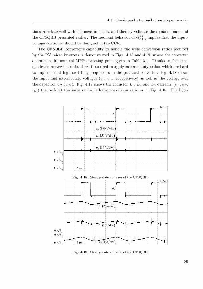
4.3. Semi-quadratic buck-boost-type inverter
tions correlate well with the measurements, and thereby validate the dynamic model of
the CFSQBB presented earlier. The resonant behavior of GSAci1-o implies that the input-
voltage controller should be designed in the CCR.
The CFSQBB converter’s capability to handle the wide conversion ratios required
by the PV micro inverters is demonstrated in Figs. 4.18 and 4.19, where the converter
operates at its nominal MPP operating point given in Table 3.1. Thanks to the semi-
quadratic conversion ratio, there is no need to apply extreme duty ratios, which are hard
to implement at high switching frequencies in the practical converter. Fig. 4.18 shows
the input and intermediate voltages (uin, uim, respectively) as well as the voltage over
the capacitor C2 (uC2). Fig. 4.19 shows the inductor L1, L2 and L3 currents (iL1, iL2,
iL3) that exhibit the same semi-quadratic conversion ratio as in Fig. 4.18. The high-
2 μs
1d
in0 V/u
( )in 10 V divu
( )im 100 V divu
im0 V/u
C20 V/u
( )C2 50 V divu
Fig. 4.18: Steady-state voltages of the CFSQBB.
2 μs
( )L2 1 A divi
1d
L20 A/i
( )L3 1 A divi
( )L1 2 A divi
L30 A/i
L10 A/i
Fig. 4.19: Steady-state currents of the CFSQBB.
89

Chapter 4. Experimental measurements
frequency noise in the inductor currents at the switching instances is due to small parasitic
capacitances between the inductor windings.
The controllers defined in Section 3.4 were implemented with a microprocessor in order
to prove the feasibility of the CFSQBB in the micro inverter application. Fig. 4.20 shows
the grid voltage (ug) and current (ug) as well as the input and intermediate voltages of
the CFSQBB inverter at steady state. The waveforms indicate a well-behaving control
system. It can be seen that the input voltage is nearly pure dc without the need for
large power decoupling capacitors to be connected at the inverter input terminals. The
transient behavior of the inverter is shown in Fig. 4.21, where the input current is stepped
from half to nominal, i.e. the figure demonstrates the CFSQBB inverter operation under
changes in the irradiance. Such fast changes are not expected in a real PV application,
but the inverter’s ability to handle them predicts that the inverter will behave well during
5 ms
( )g 1 A divi
( )g 100 V/divu
0 V
( )in 10 V divu
( )im 100 V divu
0 A0 V
Fig. 4.20: Steady-state waveforms of the CFSQBB inverter.
50 ms ( )g 0.5 A/divi
( )g 100 V/divu
0 V ( )in 10 V divu
( )im 100 V divu
0 A0 V
Fig. 4.21: CFSQBB inverter input-current step.
90

4.3. Semi-quadratic buck-boost-type inverter
0 1 2 3 4 5 6 7 80.76
0.78
0.8
0.82
0.84
0.86
0.88
0.9
0.92
0.94
Input current (A)
Eff
icie
ncy
Fig. 4.22: CFSQBB efficiency.
all the natural changes in the irradiance.
The efficiency of a PV converter is an important factor in order to estimate the return
of investment for the PV power plant and in order to compare the new converter topology
to existing ones. The efficiency of the CFSQBB converter was measured in such a way
that the operating point voltages were kept constant and the input current was varied,
which gives a good estimate of the converter efficiency under changing irradiance. The
CFSQBB efficiency is shown in Fig. 4.22 showing peak efficiency of approximately 92 %,
which is a promising figure for an early prototype converter which was not fully optimized
regarding efficiency.
91

Chapter 5. Summary of the thesis
5 SUMMARY OF THE THESIS
This chapter summarizes the thesis. A recap of the main scientific contributions and
findings in the thesis are provided with discussion on important future research topics in
the field of PV inverters that have come up during the thesis work.
5.1 Final conclusions
Grid connection is the way to fully exploit PV energy. A grid integration of the PVG
requires at least an inverter between the PVG and the utility grid, but might also contain
an additional dc-dc preregulator between the PVG and the inverter. The task of the PV
inverter is to locate the MPP of the PVG and inject maximal high-quality current to the
ultility grid. In the future, according to some studies, the inverters should include e.g.
grid voltage supporting functions in order to maintain the stability of the grid although
one inverter cannot control the grid voltage. The low efficiency of the PVG emphasizes
the necessity for low-cost high-efficiency inverters in order to make the investment on
the PV system economically feasible. One of the current solutions to the problem is the
transformerless single-stage single-phase string inverter. The transformerless inverters
are usually variations of VSI topologies with an additional input capacitor for enabling
connection to the PVG and providing power decoupling. The main concern in the trans-
formerless inverters is the elimination of ground-leakage current caused by the inverter
common-mode voltage and the stray capacitor associated to the PV modules.
The transformerless single-phase VSI-type inverters require the dc-link voltage to be
higher than the peak of the grid voltage. As a consequence, the PV input source has
to be a high-voltage string or series connection of PV modules. Optimal operation of a
string requires uniform irradiation conditions which is often not the case, especially in
the built environment. In order to reduce the detrimental effects of the partial shading
on energy production, PV-module-based micro-inverter concepts are used. The micro
inverters are prone to reduced efficiency due to the required wide conversion ratio but
have shown to be capable of outperforming the string-inverter systems, especially in the
locations susceptible to partial shading.
This thesis studied the dynamic properties of a VSI-type PV inverter and proposed
a new converter topology, known as current-fed semi-quadratic buck-boost converter,
which cascaded with an unfolding full-bridge inverter forms a transformerless PV micro
92

5.1. Final conclusions
inverter. The proposed topology is capable of handling wide conversion ratios that, with
dedicated input-voltage control, yield good power decoupling without the need to connect
a large capacitor bank to the input terminals of the converter. This thesis provides a
dynamic model and control-system-design example for the proposed converter as well
as experimental measurements proving its feasibility in the intended PV-micro-inverter
application.
The PV and other renewable-energy-based inverters have been observed to suffer from
reliability problems, reduce damping in the grid, excite harmonic resonances, and cause
harmonic distortion. These phenomena are expected to increase in the future because of
the advantageous public and political climates favoring renewable energies. Such prob-
lems can lead to production outages and compromise the stability of the utility grid.
It has been shown that the stability and oscillatory behavior of an interconnected sys-
tem composing of independently stable source and load subsystems can be assessed by
the ratio of the corresponding source and load subsystem impedances. It was shown
theoretically and by experimental measurements that negative-inceremental-resistor-like
behavior at the output of the PV inverter makes the inverter/grid interface prone to in-
stability. The negative-incremental-resistor-like behavior was observed to originate in the
VSI-type PV inverter from the cascaded control scheme, which was significantly ampli-
fied by the multiplier-based grid synchronization. The synchronization also reduced the
current-source property of the inverter by increasing the magnitude of the inverter output
admittance, which makes the inverter sensitive to harmonic grid voltages. Such behavior
cannot be studied by conventional time-domain analyses, but requires a frequency-domain
model of the inverter. It is crucial to trace the origin of such behavior in order to enable
large-scale utilization of renewable energies with minimal harm to the utility grid.
In order to construct a small-signal model of a converter, the proper selection of
input, output and state variables is of prime importance. The input variables represent
uncontrollable system inputs whereas the system outputs, i.e. the output variables, can
be controlled. The state variables are conventionally capacitor voltages and inductor
currents. The system inputs and outputs are converter terminal voltages and currents
either at the source or load side. If the converter is fed from a stiff voltage source
or the converter input current is controlled, the converter has to be analyzed as a VF
converter. If the converter is fed from a stiff current source or the converter input voltage
is controlled, the converter has to be analyzed as a CF converter. In order to transfer
maximum power, the input-side variable of the PV inverter has to be controlled. The
input-voltage control is the feasible method to track the MPP of the PVG, whereas
input-current control has been shown to suffer from controller saturation and is not
recommended. The output current of a PV inverter is controlled in order to enhance the
current-source property of the inverter and quality of the current injected to the grid.
93

Chapter 5. Summary of the thesis
In such a case, the input-voltage control is implemented by a cascaded control scheme
where an inner output-current loop controls the grid current and an outer input-voltage
loop controls the input voltage by providing the grid-current reference. Consequently,
vast majority of PV inverters have to be analyzed as CF inverters. Actually, the majority
of renewables-related inverters, such as wind power inverters, employ the same cascaded
control structure.
The PVG is internally a current source with limited output voltage and power due
to the behavior of the semiconductor junction. The PVG acts like a current source at
voltages lower than the MPP voltage (CCR) and has the properties of a voltage source
at voltages higher than the MPP voltage (CVR). Consequently, the open-loop dynamics
of the VSI in PV applications resemble the dynamics of a CF VSI in the CCR and has
the dynamic properties of a VF VSI in the CVR. However, the VF model cannot be used
because it does not suffice for the input-voltage-controlled converter. Also, the VF VSI
shows first-order dynamics, because the voltage source feeding the inverter dynamically
short circuits the input capacitor, whereas the CF VSI has an operating-point-dependent
resonance and second order dynamics as well as a RHP zero in the output-current-control
dynamics. Therefore, the use of the VF model can lead to false conclusions regarding
the current-loop stability or in the grid-interaction studies. The method to include the
non-linear behavior of the PVG to the inverter dynamics was presented, and the dynamic
model consisting of the CF inverter model and the PVG impedance was proven to be
accurate by experimental measurements using an inverter prototype fed by a real PVG.
The dynamic properties of a PVG are determined by its dynamic resistance and
capacitance. This thesis also provided the validation of a real PVG and a commercial
solar array simulator in terms of dynamic resistance and capacitance. The behavior of
the PVG dynamic resistance also supports the dual nature of the PVG: the dynamic
resistance is high in the CCR and low in the CVR, whereas the internal impedance
of an ideal current source is infinite and the internal impedance of an ideal voltage
source is zero. The validated solar array simulator was noticed to reproduce the dynamic
resistance properly but the dynamic capacitance was noticed to be considerably larger
than the capacitance of a real PVG. This can affect the behavior of the converter if its
input capacitor is small. The output impedance of the PVG shows passive-circuit-like
behavior, i.e. the phase of its output impedance lies between ±90. The solar array
simulator has to follow the same behavior in order to justify its usage as a substitute for
the real PVG, which was the case with the tested simulator proving its feasibility as a
source in the experimental measurements.
The VSI was shown to incorporate an operating-point dependent low-frequency zero in
the output-current-control dynamics, whose location on the complex plane is dependent
on the dynamic and static resistances of its input source. In the CCR, the zero lies in the
94

5.1. Final conclusions
RHP and in the CVR the zero is located in the LHP. The RHP zero, in practice, limits
the output-current-control bandwidth to the frequency of the zero. However, such low-
bandwidth output-current control has no practical usage, and therefore the current loop
is designed in the CVR, where the aforementioned zero lies in the LHP allowing stable
high-bandwidth loop. Consequently, the inverter becomes unstable when the operating
point reaches the MPP or enters the CCR under an output-current control. Therefore,
the input-voltage loop is needed for enabling stable operation in all the regions of the
PVG and not just to track the MPP.
It was shown that the operating-point dependent zero in the output-current-control
dynamics transforms into a pole in the input-voltage-control dynamics in case of the
cascaded control scheme. Consequently, the single-stage VSI in PV applications has a
RHP pole in the CCR. In case of a RHP pole in the control loop, the loop bandwidth,
in practice, has to be higher than the RHP pole frequency for stable operation with
reasonable performance. The frequency of the pole was shown to be inversely proportional
to the VSI input capacitance. This observation was used to derive a design rule for the
minimum input capacitance for the single-stage VSI in PV application based on the
stability of the input-voltage-control loop. The input-voltage control bandwidth of a
single-phase inverter is, on the other hand, limited by the inherent power fluctuation of
the single-phase grid at twice the grid freqency causing the input-voltage ripple at the
named frequency. Typically, the maximum input-voltage-control bandwidth is limited to
few tens of Hertz in order to prevent the ripple voltage passing through the input-voltage
controller and polluting the grid current reference with the second harmonic component.
Therefore, the allowed input-voltage-control bandwidth has a certain window between
the RHP pole and the ripple frequency. If the control bandwidth cannot be increased
due to the violation of the maximum control bandwidth, the input capacitance has to be
increased according to the provided design rule. Typically, the input capacitor is designed
based on e.g. the magnitude of the input-voltage ripple, which is a subjective quantity
and does not necessarily guarantee inverter stability as the new design rule does. The
feasibility of the design rule was proven experimentally, and its violation was shown to
cause subharmonic oscillation at the inverter input voltage and output current.
This thesis has provided the means and formulation for the frequency-domain mod-
eling of single-phase PV inverters. The non-linear behavior of the PVG was taken into
account by the operating-point dependent dynamic resistance and its effect on the in-
verter dynamics was presented. The methods presented in this thesis can be used as
guidelines by the researchers as well as practicing engineers in designing robust and well-
behaving PV systems.
95

Chapter 5. Summary of the thesis
5.2 Future research topics
The development of the MPP-tracking algorithms was considered to be out of the scope of
this thesis. The improvement of the existing algorithms or even invention of new ones is an
important research topic in PV systems, especially the development of algorithms capable
of locating the global MPP in partially shaded conditions. However, the MPP-tracking
algorithms typically process both the input current and voltage, which introduces both
input-voltage feedback and input-current feedforward terms to the dynamics of the PV
system, which might bring up new important observations on the properties of the system.
In some cases the tracking algorithms process output voltage and current, which will
introduce e.g. output-voltage feedforward to the system. The output-voltage feedforward
was shown to be harmful in the case of grid synchronization. The properties of the MPP-
tracking algorithms would be expected to have an effect at the low frequencies due to
their relatively slow operating speed. This kind of aspect of MPP-tracking has not been
studied.
The multiplier-based grid synchronization was shown to produce negative-incremental
resistor-like behavior at the inverter output impedance, which is one of the origins of
the grid-interaction problems. However, a multitude of different grid-synchronization
methods have been presented in the technical literature that are typically compared only
by their ability to track the grid angle as accurately as possible or their step responses
to e.g. frequency jumps in the grid. The various synchronization methods have never
been compared in terms of their effect on the inverter output impedance, although all of
the synchronization methods process the grid voltage, and therefore introduce output-
voltage feedforward which will have some effect on the output impedance of the inverter.
Such comparison could reveal which of the synchronization methods are best regarding
the minimization or even elimination of the negative-output-impedance behavior. In
addition, the emerging control methods such as the grid-voltage-supporting functions
or resonant current controllers and their possible contribution to the grid interactions
should be studied in order to enable large-scale utilization of the renewables.
The photovoltaic inverters also present various practical design issues to be solved,
such as the elimination of the common-mode current, problems regarding the use of the
new high-frequency-capable switching components and efficiency improvement as well
as minimization of electromagnetic interference issues not only at the grid side but also
at the PVG side, where the high switching frequency and long cables can introduce
interference problems.
96

BIBLIOGRAPHY
BIBLIOGRAPHY
Abbott, D. (2010). Keeping the energy depate clean: How do we supply the world’s
energy needs?, Proc. IEEE 98(1): 42–66.
Araneo, R., Lemmens, S., Grossi, M. and Bertone, S. (2009). EMC issues in high-power
grid-connected photovoltaic plants, IEEE Trans. Electromagn. Compat. 51(3): 639–
648.
Araujo, S. V., Zacharias, P. and Mallwitz, R. (2010). Highly efficient single-phase trans-
formerless inverters for grid-connected photovoltaic systems, IEEE Trans. Ind. Elec-
tron. 57(9): 3118–3128.
Balafas, C. A., Athanassopoulou, M. D., Argyropoulos, T., Skafidas, P. and Dervos, C. T.
(2010). Effect of the diffuse solar radiation on photovoltaic inverter output, 15th IEEE
Mediterranean Electrotechnical Conf. (MELECON), Malta, pp. 58–63.
Barater, D., Franceschini, G. and Lorenzani, E. (2009). Unipolar PWM for transformer-
less grid-connected converters in photovoltaic plants, Int. Conf. Clean Electrical Power
(ICCEP), Capri, Italy, pp. 387–392.
Barroso, L. A., Rudnick, H., Sensfuss, F. and Linares, P. (2010). The green effect, IEEE
Power & Energy Mag. 8(5): 22–35.
Bebic, J., Walling, R., O’Brien, K. and Kroposki, B. (2009). The sun also rises, IEEE
Power & Energy Mag. 7(3): 45–54.
Benavides, N. D. and Chapman, P. L. (2008). Modeling the effect of voltage ripple on the
power output of photovoltaic modules, IEEE Trans. Ind. Electron. 55(7): 2638–2643.
Bhowmik, A., Maitra, A., Halpin, S. M. and Schatz, J. E. (2003). Determination of
allowable penetration levels of distributed generation resources based on harmonic
limit considerations, IEEE Trans. Power Del. 18(2): 619–624.
Blaabjerg, F., Chen, Z. and Kjaer, S. B. (2004). Power electronics as efficient interface in
dispersed power generation systems, IEEE Trans. Power Electron. 19(5): 1184–1194.
Blaabjerg, F., Teodorescu, R., Liserre, M. and Timbus, A. V. (2006). Overview of control
and grid synchronization for distributed power generation systems, IEEE Trans. Ind.
Electron. 53(5): 1398–1409.
Bletterie, B., Brundlinger, R. and Lauss, G. (2011). On the characterisation of PV invert-
ers’ efficiency - introduction to the concept of achievable efficiency, Prog. Photovolt:
Res. Appl. 19(4): 423–435.
97

BIBLIOGRAPHY
Bletterie, B. and Brunner, H. (2006). Solar shadows: Does the influx of photovoltaics
endanger the quality of electricity supplies?, IEE Power Engineer 20(1): 27–29.
Bose, B. K. (2010). Global warming: Energy, environmental pollution, and the impact
of power electronics, IEEE Ind. Electron. Mag. 4(1): 6–17.
Bower, W., West, R. and Dickerson, A. (2006). Innovative PV micro-inverter topology
eliminates electrolytic capacitors for longer lifetime, IEEE 4th World Conf. Photo-
voltaic Energy Conversion (WCPEC), Waikoloa, Hawaii, U.S., pp. 2038–2041.
Bower, W. and Wiles, J. (2000). Investigation of ground-fault protection devices for pho-
tovoltaic power systems applications, 28th IEEE Photovoltaic Specialists Conference
(PVSC), Anchorage, Alaska, U.S., pp. 1378–1383.
Braun, M., Stetz, T., Brundlinger, R., Mayr, C., Hatta, H., Kobayashi, H., Ogimoto,
K., Kroposki, B., Mather, B., Coddington, M., Lynn, K., Graditi, G., Woyte, A. and
MacGill, I. (2011). Is the distribution grid ready to accept large scale photovoltaic
deployment? state of the art, progress and future prospects, Prog. Photovolt: Res.
Appl. . In press.
Brekken, T., Bhiwapurkar, N., Rathi, M., Mohan, N., Henze, C. and Moumneh, L. R.
(2002). Utility-connected power converter for maximizing power transfer from a pho-
tovoltaic source while drawing ripple-free current, 33rd Annu. IEEE Power Electronics
Specialists Conference (PESC), Cairns, Queensland, Australia, pp. 1518–1522.
Brundlinger, R., Bletterie, B., Milde, M. and Oldenkamp, H. (2006). Maximum power
point tracking performance under partially shaded PV array conditions, 21st European
Photovoltaic Solar Energy Conf. (EU PVSEC), Dresden, Germany, pp. 2157–2160.
Brundlinger, R., Henze, N., Haberlin, H., Burger, B., Bergmann, A. and Baumgartner, F.
(2009). prEN 50530 - the new european standard for performance characterisation of
PV inverters, 24th European Photovoltaic Solar Energy Conf. (EU PVSEC), Hamburg,
Germany, pp. 3105–3109.
Brundlinger, R., Henze, N., Lauss, G. and Liu, J. (2011). Module integrated power
converters - a comparison of state-of-the-art concepts and performance test results,
26th European Photovoltaic Solar Energy Conf. (EU PVSEC), Hamburg, Germany,
pp. 3204–3211.
Caamano-Martin, E., Laukamp, H., Jantsch, M., Erge, T., Thornycroft, J., de Moor, H.,
Cobben, S., Suna, D. and Gaiddon, B. (2008). Interaction between photovoltaic dis-
tributed generation and electricity networks, Prog. Photovolt: Res. Appl. 16(7): 629–
643.
98

BIBLIOGRAPHY
Calais, M., Agelidis, V. G. and Meinhardt, M. (1999). Multilevel converters for single-
phase grid connected photovoltaic systems: An overview, Solar Energy 5(5): 325–335.
Capel, A., Harpinard, J. C., Jalade, J. and Valentin, M. (1983). Current fed and volt-
age fed switching DC/DC converters - steady state and dynamic models their appli-
cations in space technology, 5th Int. Telecommunications Energy Conference (INT-
ELEC), Tokyo, Japan, pp. 421–430.
Carnieletto, R., Brandao, D. I., Suryanarayanan, S., Farret, F. A. and Simoes, M. G.
(2011). Smart grid initiative: A multifunctional single-phase voltage-source inverter,
IEEE Ind. Applicat. Mag. 17(5): 27–35.
Carrasco, J. M., Franquelo, L. G., Bialasiewicz, J. T., Galvan, E., Guisado, R. C. P.,
Prats, M. A. M., Leon, J. I. and Moreno-Alfonso, N. (2006). Power-electronic systems
for the grid integration of renewable energy sources: A survey, IEEE Trans. Ind.
Electron. 53(4): 1002–1016.
Castilla, M., Miret, J., Matas, J., de Vicuna, L. G. and Guerrero, J. M. (2008). Linear
current control scheme with series resonant harmonic compensator for single-phase
grid-connected photovoltaic inverters, IEEE Trans. Ind. Electron. 55(7): 2724–2733.
Castilla, M., Miret, J., Matas, J., de Vicuna, L. G. and Guerrero, J. M. (2009). Control
design guidelines for single-phase grid-connected photovoltaic inverters with damped
resonant harmonic compensators, IEEE Trans. Ind. Electron. 56(11): 4492–4501.
Celanovic, N. and Boroyevich, D. (2000). A comprehensive study of neutral-point voltage
balancing problem in three-level neutral-point-clamped voltage source PWM inverters,
IEEE Trans. Power Electron. 15(2): 242–249.
Cespedes, M. and Sun, J. (2009). Renewable energy systems instability involving
grid-parallel inverters, 24th Annu. IEEE Applied Power Electronics Conf. and Expo.
(APEC), Palm Springs, California, U.S., pp. 1971–1977.
Cespedes, M. and Sun, J. (2011). Modeling and mitigation of harmonic resonance between
wind turbines and the grid, IEEE Energy Conversion Congr. and Expo. (ECCE),
Phoenix, Arizona, U.S., pp. 2109–2116.
Chan, F. and Calleja, H. (2011). Reliability estimation of three single-phase topologies
in grid-connected PV systems, IEEE Trans. Ind. Electron. 58(7): 2683–2689.
Chen, S., Li, P., Brady, D. and Lehman, B. (2010). The impact of irradiance time
behaviors on inverter sizing and design, IEEE 12th Workshop on Control and Modeling
for Power Electronics (COMPEL), Boulder, Colorado, U.S., pp. 1–5.
99

BIBLIOGRAPHY
Chen, X. and Sun, J. (2011). A study of renewable energy system harmonic resonance
based on a DG test-bed, 26th Annu. IEEE Applied Power Electronics Conf. and Expo.
(APEC), Fort Worth, Texas, U.S., pp. 995–1002.
Chen, Y.-M., Chang, C.-H. and Wu, H.-C. (2009). DC-link capacitor selections for
the single-phase grid-connected PV system, Int. Conf. Power Electronics and Drive
Systems (PEDS), Taipei, Taiwan, R.O.C, pp. 72–77.
Chen, Y.-M., Wu, H.-C., Chen, Y.-C., Lee, K.-Y. and Shyu, S.-S. (2010). The AC line
current regulation strategy for the grid-connected PV system, IEEE Trans. Power
Electron. 25(1): 209–218.
Chenvidhya, D., Kirtikara, K. and Jivacate, C. (2005). PV module dynamic impedance
and its voltage and frequency dependencies, Sol. Energy Mater. Sol. Cells 86(2): 243–
251.
Chiang, S. J., Ma, T. T. and Lee, M. J. (2009). Design and implementation of boost-type
flyback PV inverter, Int. Conf. Power Electronics and Drive Systems (PEDS), Taipei,
Taiwan, R.O.C, pp. 72–77.
Chicco, G., Schlabbach, J. and Spertino, F. (2009). Experimental assessment of the wave-
form distortion in grid-connected photovoltaic installations, Solar Energy 83(7): 1026–
1039.
Choi, W.-Y. and Lee, C.-G. (2012). Photovoltaic panel integrated power conditioning
system using a high efficiency step-up DC-DC converter, Renewable Energy 41: 227–
234.
Ciobotaru, M., Agelidis, V. G., Teodorescu, R. and Blaabjerg, F. (2010). Accurate and
less-disturbing active antiislanding method based on PLL for grid-connected convert-
ers, IEEE Trans. Power Electron. 25(6): 1576–1584.
Deline, C. (2009). Partially shaded operation of a grid-tied PV system, IEEE 34th Pho-
tovoltaic Specialists Conference (PVSC), Philadelphia, Pennsylvania, U.S., pp. 1268–
1273.
Dorf, R. C. and Bishop, R. H. (2001). Modern Control Systems, 9th edn, Prentice-Hall
Inc., U.S.
Eltawil, M. A. and Zhao, Z. (2010). Grid-connected photovoltaic power systems: technical
and potential problems - a review, Renew. Sust. Energy Rev. 14(1): 112–129.
Enslin, J. H. R. (2005). Opportunities in hybrid energy networks using power electronic
interfaces, Int. Conf. Future Power Systems (FPS), Amsterdam, Netherlands, pp. 1–7.
100

BIBLIOGRAPHY
Enslin, J. H. R. and Heskes, P. J. M. (2004). Harmonic interaction between a large num-
ber of distributed power inverters and the distribution network, IEEE Trans. Power
Electron. 19(6): 1586–1593.
Erickson, R. W. and Rogers, A. P. (2009). A microinverter for building-integrated pho-
tovoltaics, 24th Annu. IEEE Applied Power Electronics Conf. and Expo. (APEC),
Washington, D.C., U.S., pp. 911–917.
Esram, T. and Chapman, P. L. (2007). Comparison of photovoltaic array maximum
power point tracking techniques, IEEE Trans. Energy Convers. 22(2): 439–449.
Franklin, G. F., Powell, J. D. and Workman, M. (1998). Digital Control of Dynamic
Systems, 3rd edn, Addison Wesley Longman, Inc., USA. 742 pp.
Fratta, A., Griffero, G., Guglielmi, P., Nieddu, S. and Villata, F. (2002). Minimum
capacitor size in DC/DC/AC converters by means of novel PWM technique and DC-
link structure, IEEE Int. Symp. Industrial Electronics (ISIE), Vol. 3, L’Aquila, Italy,
pp. 789–794.
Garcia, M., Maruri, J. M., Marroyo, L., Lorenzo, E. and Perez, M. (2008). Partial
shadowing, MPPT performance and inverter configurations: observations at tracking
PV plants, Prog. Photovolt: Res. Appl. 16(6): 529–536.
Gonzalez, R., Gubia, E., Lopez, J. and Marroyo, L. (2008). Transformerless single-phase
multilevel-based photovoltaic inverter, IEEE Trans. Ind. Electron. 55(7): 2694–2702.
Gonzalez, R., Lopez, J., Sanchis, P. and Marroyo, L. (2007). Transformerless inverter for
single-phase photovoltaic systems, IEEE Trans. Power Electron. 22(2): 693–697.
Green, M. A. (2005). Silicon photovoltaic modules: A brief history of the first 50 years,
Prog. Photovolt: Res. Appl. 13(5): 447–455.
Green, M. A., Emery, K., Hishikawa, Y., Warta, W. and Dunlop, E. D. (2012). Solar cell
efficiency tables (version 39), Prog. Photovolt: Res. Appl. 20(1): 12–20.
Gu, B. G. and Nam, K. (2005). A theoretical minimum DC-link capacitance in PWM
converter-inverter systems, IEE Proc. - Electr. Power Appl. 152(1): 81–88.
Gubia, E., Sanchis, P., Ursua, A., Lopez, J. and Marroyo, L. (2007). Ground cur-
rents in single-phase transformerless photovoltaic systems, Prog. Photovolt: Res. Appl.
15(7): 629–650.
Heskes, P. J. M., Myrzik, J. M. A. and Kling, W. L. (2010). Harmonic distortion and os-
cillatory voltages and the role of negative impedance, IEEE Power and Energy Society
General Meeting, Minneapolis, Minnesota, U.S., pp. 1–7.
101
BIBLIOGRAPHY
Hu, H., Harb, S. and Kutkut, N. (2010). Power decoupling techniques for micro-inverters
in PV systems - a review, IEEE Energy Conversion Congress and Expo. (ECCE),
Atlanta, Georgia, U.S., pp. 3235–3240.
IEA (9.3. 2012). Key world energy statistics 2011, Technical report, International Energy
Agency. Available from http://www.iea.org/.
Kadri, R., Gaubert, J.-P. and Champenois, G. (2011). An improved maximum power
point tracking for photovoltaic grid-connected inverter based on voltage-oriented con-
trol, IEEE Trans. Ind. Electron. 58(1): 66–75.
Kakimoto, N., Satoh, H., Takayama, S. and Nakamura, K. (2009). Ramp-rate control
of photovoltaic generator with electric double-layer capacitor, IEEE Trans. Energy
Convers. 24(2): 465–473.
Kang, F.-S., Park, S.-J., Cho, S. E. and Kim, J. M. (2005). Photovoltaic power interface
circuit incorporated with a buck-boost converter and a full-bridge inverter, Applied
Energy 82(3): 266–283.
Kerekes, T., Teodorescu, R. and Borup, U. (2007). Transformerless photovoltaic invert-
ers connected to the grid, 22nd Annu. IEEE Applied Power Electronics Conference
(APEC), Anaheim, California, U.S., pp. 1733–1737.
Kerekes, T., Teodorescu, R., Rodriguez, P., Vasquez, G. and Aldabas, E. (2011). A new
high-efficiency single-phase transformerless PV inverter topology, IEEE Trans. Ind.
Electron. 58(1): 184–191.
Khalifa, A. S. and El-Saadany, E. F. (2011). Control of three-phase grid-connected
photovoltaic arrays with open loop maximum power point tracking, IEEE Power and
Energy Society General Meeting, Detroit, Michigan, U.S., pp. 1–8.
Kjaer, S. B., Pedersen, J. K. and Blaabjerg, F. (2005). A review of single-phase grid-
connected inverters for photovoltaic modules, IEEE Trans. Ind. Appl. 41(5): 1292–
1306.
Kobayashi, K., Takano, I. and Sawada, Y. (2006). A study of a two stage maximum
power point tracking control of a photovoltaic system under partially shaded insolation
conditions, Sol. Energy Mater. Sol. Cells 90(18/19): 2975–2988.
Kolar, J. W., Friedli, T., Krismer, F., Looser, A., Schweizer, M., Steimer, P. and Bevirt,
J. (2011). Conceptualization and multi-objective optimization of the electric system
of an airborne wind turbine, IEEE Int. Symp. Industrial Electronics (ISIE), Gdansk,
Poland, pp. 32–55.
102

BIBLIOGRAPHY
Kotsopoulos, A., Duarte, J. L. and Hendrix, M. A. M. (2001). A predictive control
scheme for DC voltage and AC current in grid-connected photovoltaic inverters with
minimum DC link capacitance, 27th Annu. Conf. IEEE Industrial Electronics Society
(IECON), Denver, Colorado, U.S., pp. 1994–1999.
Kroposki, B., Margolis, R. and Ton, D. (2009). Harnessing the sun: An overview of solar
technologies, IEEE Power & Energy Mag. 7(3): 22–33.
Kumar, R. A., Suresh, M. S. and Nagaraju, J. (2006). Effect of solar array capacitance on
the performance of switching shunt regulator, IEEE Trans. Power Electron. 21(2): 543–
548.
Kwon, J.-M., Kwon, B.-H. and Nam, K.-H. (2009). High-efficiency module-integrated
photovoltaic power conditioning system, IET Power Electron. 2(4): 410–420.
Kwon, J.-M., Nam, K.-H. and Kwon, B.-H. (2006). Photovoltaic power conditioning
system with line connection, IEEE Trans. Ind. Electron. 53(4): 1048–1054.
Lai, J.-S. (2009). Power conditioning circuit topologies: power conversion from low-
voltage dc to high-voltage ac for single-phase grid-tie applications, IEEE Ind. Electron.
Mag. 3(2): 24–34.
Leppaaho, J., Huusari, J., Nousiainen, L., Puukko, J. and Suntio, T. (2011). Dynamic
properties and stability assessment of current-fed converters in photovoltaic applica-
tions, IEEJ Trans. Ind. Applicat. 131(8): 976–984.
Leppaaho, J., Nousiainen, L., Puukko, J., Huusari, J. and Suntio, T. (2010). Implement-
ing current-fed converters by adding an input capacitor at the input of voltage-fed
converter for interfacing solar generator, 14th Int. Power Electronics and Motion Con-
trol Conf. (EPE-PEMC), Ohrid, Macedonia, pp. T12–81–T12–88.
Leppaaho, J. and Suntio, T. (2011). Dynamic characteristics of current-fed superbuck
converter, IEEE Trans. Power Electron. 26(1): 200–209.
Li, Q. and Wolfs, P. (2008). A review of the single phase photovoltaic module integrated
converter topologies with three different DC link configurations, IEEE Trans. Power
Electron. 23(3): 1320–1333.
Li, W. and He, X. (2011). Review of nonisolated high-step-up DC/DC converters in pho-
tovoltaic grid-connected applications, IEEE Trans. Ind. Electron. 58(4): 1239–1250.
Li, Y. and Oruganti, R. (2012). A low cost flyback CCM inverter for AC module appli-
cation, IEEE Trans. Power Electron. 27(3): 1295–1303.
103

BIBLIOGRAPHY
Liao, Y.-H. and Lai, C.-M. (2011). Newly-constructed simplified single-phase multistring
multilevel inverter topology for distributed energy resources, IEEE Trans. Power Elec-
tron. 26(9): 2386–2392.
Liserre, M., Blaabjerg, F. and Dell’Aquila, A. (2004). Step-by-step design procedure
for a grid-connected three-phase PWM voltage source converter, Int. J. Electronics
91(8): 445–460.
Liserre, M., Teodorescu, R. and Blaabjerg, F. (2006). Stability of photovoltaic and wind
turbine grid-connected inverters for a large set of grid impedance values, IEEE Trans.
Power Electron. 21(1): 263–272.
Liu, B., Duan, S. and Cai, T. (2011). Photovoltaic DC-building-module-based BIPV
system - concept and design considerations, IEEE Trans. Power Electron. 26(5): 1418–
1429.
Liu, S. and Dougal, R. A. (2002). Dynamic multiphysics model for solar array, IEEE
Trans. Energy Convers. 17(2): 285–294.
Lopez, O., Freijedo, F. D., Yepes, A. G., Fernandez-Comesana, P., Malvar, J., Teodor-
escu, R. and Doval-Gandoy, J. (2010). Eliminating ground current in a transformerless
photovoltaic application, IEEE Trans. Energy Convers. 25(1): 140–147.
Luoma, J., Kleissl, J. and Murray, K. (2012). Optimal inverter sizing considering cloud
enhancement, Solar Energy 86(1): 421–429.
Maki, A. and Valkealahti, S. (2012). Power losses in long string and parallel-connected
short strings of series-connected silicon-based photovoltaic modules due to partial shad-
ing conditions, IEEE Trans. Energy Convers. 27(1): 173–183.
Maki, A., Valkealahti, S. and Leppaaho, J. (2011). Operation of series connected silicon-
based photovoltaic modules under partial shading conditions, Prog. Photovolt: Res.
Appl. . In press.
Maki, A., Valkealahti, S. and Suntio, T. (2010). Dynamic terminal characteristics of a
photovoltaic generator, 14th Int. Power Electronics and Motion Control Conf. (EPE-
PEMC), Ohrid, Macedonia, pp. T12–76–T12–80.
Masoum, M. A. S., Dehbonei, H. and Fuchs, E. F. (2002). Theoretical and experimental
analyses of photovoltaic systems with voltage- and current-based maximum power-
point tracking, IEEE Trans. Energy Convers. 17(4): 514–522.
104

BIBLIOGRAPHY
Messo, T., Puukko, J. and Suntio, T. (2012). Effect of MPP-tracking dc/dc converter
on VSI-based photovoltaic inverter dynamics, 6th IET Int. Conf. Power Electronics,
Machines and Drives (PEMD), Bristol, U.K., pp. 1–6.
Middlebrook, R. D. (1976). Input filter considerations in design and applications
of switching regulators, IEEE Industry Applications Society Annu. Meeting Rec.,
Chicago, Illinois, U.S., pp. 366–382.
Middlebrook, R. D. and Cuk, S. (1977). A general unified approach to modelling
switching-converter power stages, Int. J. Electronics 42(6): 521–550.
Mohamed, Y. A.-R. I. (2011). Mitigation of dynamic, unbalanced, and harmonic voltage
disturbances using grid-connected inverters with LCL filter, IEEE Trans. Ind. Electron.
58(9): 3914–3924.
Mohd, A. (2011). The evolution of PV solar power architectures: A quantative analysis
of micro-inverters’ performance vs. conventional inverters, 26th European Photovoltaic
Solar Energy Conf. (EU PVSEC), Hamburg, Germany, pp. 3739–3744.
Myrzik, J. M. A. and Calais, M. (2003). String and module integrated inverters for
single-phase grid connected photovoltaic systems - a review, IEEE Bologna PowerTech
Conf.
Nian, H. and Zeng, R. (2011). Improved control strategy for stand-alone distributed
generation system under unbalanced and non-linear loads, IET Renew. Power Gener.
5(5): 323–331.
Ninad, N. A. and Lopes, L. A. C. (2007). Operation of single-phase grid-connected in-
verters with large DC bus voltage ripple, IEEE Canada Electrical Power Conf. (EPC),
Montreal, Quebec, Canada, pp. 172–176.
Nonaka, S. (1994). A utility-connected residential PV system adapted a novel single-
phase composite PWM voltage source inverter, IEEE 1st World Conf. Photovoltaic
Energy Conversion (WCPEC), Waikoloa, Hawaii, U.S., pp. 1064–1068.
Nousiainen, L., Puukko, J. and Suntio, T. (2011a). Appearance of a RHP-zero in VSI-
based photovoltaic converter control dynamics, 33rd Int. Telecommunications Energy
Conf. (INTELEC), Amsterdam, Netherlands, pp. 1–8.
Nousiainen, L., Puukko, J. and Suntio, T. (2011b). Simple VSI-based single-phase in-
verter: dynamical effect of photovoltaic generator and multiplier-based grid synchro-
nization, IET Renewable Power Generation Conf., Edinburgh, U.K., pp. 1–6.
105

BIBLIOGRAPHY
Nousiainen, L. and Suntio, T. (2011). Dynamic characteristics of current-fed semi-
quadratic buck-boost converter in photovoltaic applications, IEEE Energy Conversion
Congr. and Expo. (ECCE), Phoenix, Arizona, U.S., pp. 1031–1038.
Oldenkamp, H., de Jong, I., van der Borg, N., de Boer, B., de Moor, H. and Sinke, W. C.
(2004). PV-wirefree versus conventional PV-systems: Detailed analysis of difference in
energy yield between series and parallel connected PV-modules, 19th European Pho-
tovoltaic Solar Energy Conf. (EU PVSEC), Paris, France, pp. 1–4.
Parida, B., Iniyan, S. and Goic, R. (2011). A review of solar photovoltaic technologies,
Renew. Sust. Energy Rev. 15(3): 1625–1636.
Park, J.-H., Ahn, J.-Y., Cho, B.-H. and Yu, G.-J. (2006). Dual-module-based maxi-
mum power point tracking control of photovoltaic systems, IEEE Trans. Ind. Electron.
53(4): 1036–1047.
Patel, H. and Agarwal, V. (2008). Maximum power point tracking scheme for PV systems
operating under partially shaded conditions, IEEE Trans. Ind. Electron. 55(4): 1689–
1698.
Petrone, G., Spagnuolo, G., Teodorescu, R., Veerachary, M. and Vitelli, M. (2008). Re-
liability issues in photovoltaic power processing systems, IEEE Trans. Ind. Electron.
55(7): 2569–2580.
Popovic-Gerber, J., Ferreira, J. A. and van Wyk, J. D. (2011). Quantifying the value of
power electronics in sustainable electrical energy systems, IEEE Trans. Power Electron.
26(12): 3534–3544.
Prapanavarat, C., Barnes, M. and Jenkins, N. (2002). Investigation of the performance
of a photovoltaic AC module, IEE Proc.-Gener. Transm. Distrib. 149(4): 472–478.
Puukko, J., Messo, T. and Suntio, T. (2011). Effect of photovoltaic generator on a typical
VSI-based three-phase grid-connected photovoltaic inverter dynamics, IET Renewable
Power Generation Conf., Edinburgh, U.K., pp. 1–6.
Puukko, J., Nousiainen, L., Maki, A., Messo, T., Huusari, J. and Suntio, T. (2012).
Photovoltaic generator as an input source for power electronic converters, 15th Int.
Power Electronics and Motion Control Conf. (EPE-PEMC 2012 ECCE Europe), Novi
Sad, Serbia, pp. 1–8.
Rahman, S. (2003). Green power: what is it and where can we find it?, IEEE Power &
Energy Mag. 1(1): 30–37.
106

BIBLIOGRAPHY
Ramabadran, R. and Mathur, B. (2009). Effect of shading on series and parallel connected
solar PV modules, Modern Applied Science 3(10): 32–41.
Razykov, T. M., Ferekides, C. S., Morel, D., Stefanakos, E., Ullal, H. S. and Upadhyaya,
H. M. (2011). Solar photovoltaic electricity: Current status and future prospects, Solar
Energy 85(8): 1580–1608.
Recart, F. and Cuevas, A. (2006). Application of junction capacitance measurements to
the characterization of solar cells, IEEE Trans. Electron Devices 53(3): 442–448.
Rodriguez, C. and Amaratunga, G. A. J. (2008). Long-lifetime power inverter for pho-
tovoltaic AC modules, IEEE Trans. Ind. Electron. 55(7): 2593–2601.
Roman, E., Alonso, R., Ibanez, P., Elorduizapatarietxe, S. and Goitia, D. (2006).
Intelligent PV module for grid-connected PV systems, IEEE Trans. Ind. Electron.
53(4): 1066–1073.
Sahan, B., Araujo, S. V., Nodling, C. and Zacharias, P. (2011). Comparative evaluation
of three-phase current source inverters for grid interfacing of distributed and renewable
energy systems, IEEE Trans. Power Electron. 26(8): 2304–2318.
Salas, V., Olias, E., Alonso, M. and Chenlo, F. (2008). Overview of the legistlation of
DC injection in the network for low voltage small grid-connected PV systems in Spain
and other countries, Renew. Sust. Energy Rev. 12(2): 575–583.
Schonberger, J. (2009). A single-phase multi-string PV inverter with minimal bus capac-
itance, 13th European Conf. Power Electronics and Applications (EPE), Barcelona,
Spain, pp. 1–10.
Shimizu, T., Wada, K. and Nakamura, N. (2006). Flyback-type single-phase utility inter-
active inverter with power pulsation decoupling on the DC input for an AC photovoltaic
module system, IEEE Trans. Power Electron. 21(5): 1264–1272.
Silvestre, S., Boronat, A. and Chouder, A. (2009). Study of bypass diodes configuration
on PV modules, Applied Energy 86(9): 1632–1640.
Simmons, A. D. and Infield, D. G. (2000). Current waveform quality from grid-connected
photovoltaic inverters and its dependence on operating conditions, Prog. Photovolt:
Res. Appl. 8(4): 411–420.
Skogestad, S. and Postlethwaite, I. (1998). Multivariable feedback control, John Wiley &
Sons Ltd, England. 559 pp.
107

BIBLIOGRAPHY
Sullivan, C. R., Awerbuch, J. and Latham, A. M. (2011). Decrease in photovoltaic power
output from ripple: Simple general calculation and effect of partial shading, 26th Annu.
IEEE Applied Power Electronics Conf. and Expo. (APEC), Fort Worth, Texas, U.S.,
pp. 1954–1960.
Sun, J. (2008). AC power electronic systems: stability and power quality, 11th Workshop
Control and Modeling for Power Electronics (COMPEL), Zurich, Switzerland, pp. 1–
10.
Sun, J. (2011). Impedance-based stability criterion for grid-connected inverters, IEEE
Trans. Power Electron. 26(11): 3075–3078.
Suntio, T. (2009). Dynamic Profile of Switched-Mode Converter: Modeling, Analysis and
Control, Wiley-VCH, Germany. 357 pp.
Suntio, T. (2012). Issues on interfacing problematics in PV generator and MPP-tracking
converters, in R. D. Rugescu (ed.), Solar Power, InTech, chapter 14, pp. 239–260.
ISBN 978-953-51-0014-0.
Suntio, T., Puukko, J., Nousiainen, L., Messo, T. and Huusari, J. (2011). Change of
paradigm in power electronic converters used in renewable energy applications, 33rd
IEEE Int.Telecommunications Energy Conf. (INTELEC), Amsterdam, Netherlands,
pp. 1–9.
Tan, G. H., Wang, J. Z. and Ji, Y. C. (2007). Soft-switching flyback inverter with
enhanced power decoupling for photovoltaic applications, IET Electr. Power Appl.
1(2): 264–274.
Teodorescu, R., Liserre, M. and Rodrıguez, P. (2011). Grid Converters for Photovoltaic
and Wind Power Systems, 2nd edn, John Wiley & Sons, Ltd., UK. 398 pp.
Thongrpon, J., Kirtikara, K. and Jivacate, C. (2006). A method for the determination
of dynamic resistance of photovoltaic modules under illumination, Sol. Energy Mater.
Sol. Cells 90(18–19): 3078–3084.
Tofoli, F. L., Schonell, J. C., Gallo, C. A. and Sanhueza, S. M. R. (2009). A low cost
single-phase grid-connected photovoltaic system with reduced complexity, Brazilian
Power Electronics Conf. (COBEP), Bonito, Brazil, pp. 1033–1038.
Tse, C. K. (1998). Linear Circuit Analysis, Addison Wesley Longman, Inc., UK. 307 pp.
Valkealahti, S. (2011). Forecasting the future of renewables, in J. Blanco and H. Kherad-
mand (eds), Climate Change - Socioeconomic Effects, InTech, chapter 22, pp. 425–440.
ISBN 978-953-307-411-5.
108

BIBLIOGRAPHY
Vasquez, J. C., Guerrero, J. M., Luna, A., Rodriguez, P. and Teodorescu, R. (2009).
Adaptive droop control applied to voltage-source inverters operating in grid-connected
and islanded modes, IEEE Trans. Ind. Electron. 56(10): 4088–4096.
Vighetti, S., Ferrieux, J.-P. and Lembeye, Y. (2012). Optimization and design of a
cascaded DC/DC converter devoted to grid-connected photovoltaic systems, IEEE
Trans. Power Del. 27(4): 2018–2027.
Villanueva, E., Correa, P., Rodriguez, J. and Pacas, M. (2009). Control of a single-phase
cascaded H-bridge multilevel inverter for grid-connected photovoltaic systems, IEEE
Trans. Ind. Electron. 56(11): 4399–4406.
Vitorino, M. A. and de Rossiter Correa, M. B. (2011). Compensation of DC link oscil-
lation in single-phase VSI and CSI converters for photovoltaic grid connection, IEEE
Energy Conversion Congr. and Expo. (ECCE), Phoenix, Arizona, U.S., pp. 2007–2014.
Wang, F., Duarte, J. L., Hendrix, M. A. M. and Ribeiro, P. F. (2011). Modeling and
analysis of grid harmonic distortion impact of aggregated DG inverters, IEEE Trans.
Power Electron. 26(3): 786–797.
Wang, Y.-J. and Hsu, P.-C. (2010). Analytical modelling of partial shading and different
orientation of photovoltaic modules, IET Renew. Power Gener. 4(3): 272–282.
Watt, G., Kaizuka, I., Husser, P. and Brundlinger, R. (2011). Trends in photovoltaic
applications - the latest survey results on PV market, industry and policies from the
IEA PVPS programme, 26th European Photovoltaic Solar Energy Conf. (EU PVSEC),
Hamburg, Germany, pp. 4527–4530.
Woyte, A., Nijs, J. and Belmans, R. (2003). Partial shadowing of photovoltaic arrays with
different system configurations: literature review and field test results, Solar Energy
74(3): 217–233.
Wu, J.-F., Chang, C.-H., Lin, L.-C. and Kuo, C.-L. (2011). Power loss comparison
of single- and two-stage grid connected photovoltaic systems, IEEE Trans. Energy
Convers. 26(2): 707–715.
Wyatt, J. and Chua, L. (1983). Nonlinear resistive maximum power theorem, with solar
cell application, IEEE Trans. Circuits Syst. 30(11): 824–828.
Xiao, H. and Xie, S. (2010). Leakage current analytical model and application in single-
phase transformerless photovoltaic grid-connected inverter, IEEE Trans. Electromagn.
Compat. 52(4): 902–913.
109

BIBLIOGRAPHY
Xiao, H., Xie, S., Chen, Y. and Huang, R. (2011). An optimized transformerless photo-
voltaic grid-connected inverter, IEEE Trans. Ind. Electron. 58(5): 1887–1895.
Xiao, W., Dunford, W. G., Palmer, P. R. and Capel, A. (2007). Regulation of photovoltaic
voltage, IEEE Trans. Ind. Electron. 54(3): 1365–1374.
Xue, Y., Chang, L., Kjaer, S. B., Bordonau, J. and Shimizu, T. (2004). Topologies
of single-phase inverters for small distributed power generators: An overview, IEEE
Trans. Power Electron. 19(5): 1305–1314.
Yang, B., Li, W., Gu, Y., Cui, W. and He, X. (2012). Improved transformerless inverter
with common-mode leakage current elimination for a photovoltaic grid-connected
power system, IEEE Trans. Power Electron. 27(2): 752–762.
Yao, Z., Xiao, L. and Yan, Y. (2010). Seamless transfer of single-phase grid-interactive
inverters between grid-connected and stand-alone modes, IEEE Trans. Power Electron.
25(6): 1597–1603.
Yazdani, A. and Dash, P. P. (2009). A control methology and characterization of dy-
namics for a photovoltaic (PV) system interfaced with a distribution network, IEEE
Trans. Power Del. 24(3): 1538–1551.
Yu, W., Lai, J.-S., Qian, H. and Hutchens, C. (2011). High-efficiency MOSFET inverter
with H6-type configuration for photovoltaic nonisolated AC-module applications, IEEE
Trans. Power Electron. 26(4): 1253–1260.
Zhang, L., Sun, K., Xing, Y., Feng, L. and Ge, H. (2011). A modular grid-connected pho-
tovoltaic generation system based on dc bus, IEEE Trans. Power Electron. 26(2): 523–
531.
110
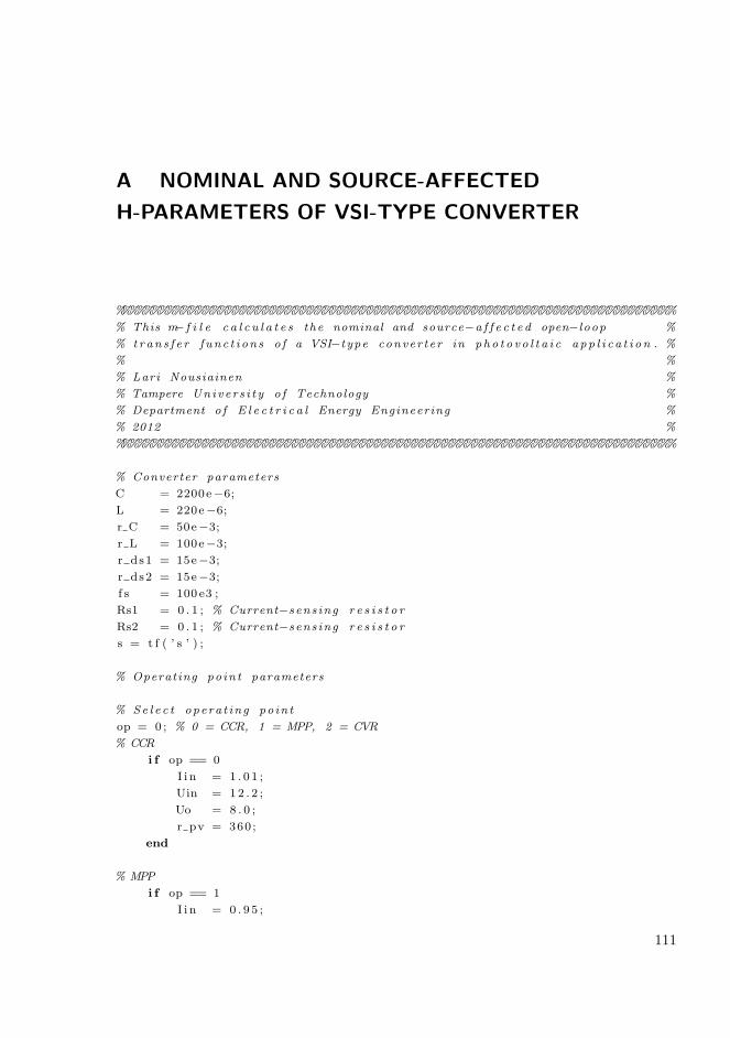
A NOMINAL AND SOURCE-AFFECTED
H-PARAMETERS OF VSI-TYPE CONVERTER
%%%%%%%%%%%%%%%%%%%%%%%%%%%%%%%%%%%%%%%%%%%%%%%%%%%%%%%%%%%%%%%%%%%%%%%%%%%
% This m− f i l e c a l c u l a t e s the nominal and source−a f f e c t e d open−l oop %
% t ran s f e r f unc t i ons o f a VSI−type conver ter in pho t o v o l t a i c a pp l i c a t i on . %
% %
% Lari Nousiainen %
% Tampere Unive r s i t y o f Technology %
% Department o f E l e c t r i c a l Energy Engineering %
% 2012 %
%%%%%%%%%%%%%%%%%%%%%%%%%%%%%%%%%%%%%%%%%%%%%%%%%%%%%%%%%%%%%%%%%%%%%%%%%%%
% Converter parameters
C = 2200e−6;
L = 220e−6;
r C = 50e−3;
r L = 100e−3;
r d s1 = 15e−3;
r d s2 = 15e−3;
f s = 100 e3 ;
Rs1 = 0 . 1 ; % Current−sens ing r e s i s t o r
Rs2 = 0 . 1 ; % Current−sens ing r e s i s t o r
s = t f ( ’ s ’ ) ;
% Operating po in t parameters
% Se l e c t opera t ing po in t
op = 0 ; % 0 = CCR, 1 = MPP, 2 = CVR
% CCR
i f op == 0
I i n = 1 . 0 1 ;
Uin = 12 . 2 ;
Uo = 8 . 0 ;
r pv = 360 ;
end
% MPP
i f op == 1
I i n = 0 . 9 5 ;
111

Appendix A. Nominal and source-affected H-parameters of VSI-type converter
Uin = 15 . 6 ;
Uo = 8 . 0 ;
r pv = 16 . 4 ;
end
% CVR
i f op == 2
I i n = 0 . 7 1 ;
Uin = 17 . 4 ;
Uo = 8 . 0 ;
r pv = 4 . 0 ;
end
% Steady−s t a t e s o l u t i on
duty = [ Uin+r C∗ I in , −(( r C+r ds1−r d s2+Rs1−Rs2 )∗ I i n+Uo ) , . . .
−(r L+r ds2+Rs2 )∗ I i n ] ;
R = roots ( duty ) ;
D = R( 1 ) ; % Duty r a t i o
D1 = 1−D; % Complementary duty r a t i o
Uc = Uin ;
IL = I i n /D;
Io = I i n /D;
% Sta te matr ices
R1 = r L + D∗( r C + r ds1 + Rs1 ) + D1∗( r d s2 + Rs2 ) ;
U1 = Uin + r C∗ I i n − ( r C + r ds1 − r d s2 + Rs1 − Rs2 )∗ I i n /D;
Am = [−R1/L , D/L
−D/C, 0 ] ;
Bm = [D∗ r C/L , −1/L , U1/L
1/C, 0 , −I i n /D/C ] ;
Cm = [−D∗r C , 1
1 , 0 ] ;
Dm = [ r C , 0 , −r C∗ I i n /D
0 , 0 , 0 ] ;
Im = eye ( 2 ) ;
% H−parameters
Hpar = Cm ∗ inv ( s ∗Im − Am) ∗ Bm + Dm;
Hpar = minrea l (Hpar ) ;
Zin = Hpar ( 1 , 1 ) ;
Toi = Hpar ( 1 , 2 ) ;
Gci = Hpar ( 1 , 3 ) ;
Gio = Hpar ( 2 , 1 ) ;
Yo = −Hpar ( 2 , 2 ) ;
Gco = Hpar ( 2 , 3 ) ;
% Source−a f f e c t e d H−parameters
112

Ys = 1/ r pv ;
Zin oco = Zin + Toi∗Gio/Yo ;
Z i n i n f = Zin − Gio∗Gci/Gco ;
Zin SA = Zin /(1 + Ys∗Zin ) ;
Toi SA = Toi /(1 + Ys∗Zin ) ;
Gci SA = Gci /(1 + Ys∗Zin ) ;
Gio SA = Gio /(1 + Ys∗Zin ) ;
Yo SA = (1 + Ys∗Zin oco )/(1 + Ys∗Zin )∗Yo ;
Gco SA = (1 + Ys∗ Z i n i n f )/(1 + Ys∗Zin )∗Gco ;
113

Appendix B. Nominal and source-affected H-parameters of CFSQBB converter
B NOMINAL AND SOURCE-AFFECTED
H-PARAMETERS OF CFSQBB CONVERTER
%%%%%%%%%%%%%%%%%%%%%%%%%%%%%%%%%%%%%%%%%%%%%%%%%%%%%%%%%%%%%%%%%%%%%%%%%%%
% This m− f i l e c a l c u l a t e s the nominal and source−a f f e c t e d open−l oop %
% t ran s f e r f unc t i ons o f a CFSQBB conver ter in pho t o v o l t a i c a pp l i c a t i on . %
% %
% Lari Nousiainen %
% Tampere Unive r s i t y o f Technology %
% Department o f E l e c t r i c a l Energy Engineering %
% 2012 %
%%%%%%%%%%%%%%%%%%%%%%%%%%%%%%%%%%%%%%%%%%%%%%%%%%%%%%%%%%%%%%%%%%%%%%%%%%%
% Converter parameters
Uim = 370 ;
Uo = 230 ;
r C1 = 0 . 3 ;
r C3 = 0 . 1 ;
r C2 = 0 . 1 ;
r L1 = 0 . 0 8 ;
r L2 = 0 . 3 ;
r L3 = 0 . 3 ;
C1 = 20e−6;
C3 = 660e−6;
C2 = 20e−6;
L1 = 220e−6;
L2 = 1e−3;
L3 = 1e−3;
f s = 150 e3 ;
Ts = 1/ f s ;
% Operating po in t parameters
% Se l e c t opera t ing po in t
op = 0 ; % 0 = CCR, 1 = MPP, 2 = CVR
% CCR
114

i f op == 0
I i n = 7 . 8 4 ;
Uin = 15 ;
r pv = 56 ;
end
% MPP
i f op == 1
I i n = 7 . 3 3 ;
Uin = 25 . 9 ;
r pv = 3 . 5 ;
end
% CVR
i f op == 2
I i n = 5 . 7 ;
Uin = 29 ;
r pv = 0 . 8 ;
end
% Nominal open−l oop t r an s f e r f unc t i ons
a = I i n ∗( r C1 + r C3 − r L2 ) ;
b = (Uim − I i n ∗ r C2 + I i n ∗ r L2 ) ;
c = I i n ∗ r C2 ;
d = I i n ∗ r L1 − Uin ;
D1 roots = roots ( [ a b c d ] ) ;
D1 = D1 roots ( 3 ) ;
a = Uim ;
b = −D1ˆ2∗ I i n ∗( r C1 + r C3 ) − Uo ;
c = −D1ˆ2∗ I i n ∗ r L3 ;
D2p roots = roots ( [ a b c ] ) ;
D2p = D2p roots ( 1 ) ;
D2 = 1 − D2p ;
I L1 = I i n ;
I L2 = D1∗ I i n ;
I L3 = D1ˆ2∗ I i n /(1−D2 ) ;
U C1 = Uin ;
U C3 = Uim − Uin ;
U C2 = D1∗Uim + D1∗ I i n ∗ r L2 + D1ˆ2∗ I i n ∗( r C1 + r C3 − r L2 ) ;
% Dynamic Model
s = t f ( ’ s ’ ) ;
115

Appendix B. Nominal and source-affected H-parameters of CFSQBB converter
% Matrices
A11 = 0 ;
A12 = 0 ;
A13 = 0 ;
A14 = −1/C1 ;
A15 = D1/C1 ;
A16 = −D2p/C1 ;
A21 = 0 ;
A22 = 0 ;
A23 = 0 ;
A24 = 0 ;
A25 = D1/C3 ;
A26 = −D2p/C3 ;
A31 = 0 ;
A32 = 0 ;
A33 = 0 ;
A34 = D1/C2 ;
A35 = −1/C2 ;
A36 = 0 ;
A41 = 1/L1 ;
A42 = 0 ;
A43 = −D1/L1 ;
A44 = (−r C1 − r L1 − D1∗ r C2 )/L1 ; %% −R1/L1
A45 = D1∗( r C1 + r C2 )/L1 ; %% R2/L1
A46 = −r C1∗D2p/L1 ;
A51 = −D1/L2 ;
A52 = −D1/L2 ;
A53 = 1/L2 ;
A54 = D1∗( r C1 + r C2 )/L2 ; %% R2/L2
A55 = (−r C2 − r L2 − D1∗( r C1 + r C3 − r L2 ) )/L2 ; %% −R3/L2
A56 = 0 ;
A61 = D2p/L3 ;
A62 = D2p/L3 ;
A63 = 0 ;
A64 = −D2p∗ r C1/L3 ;
A65 = 0 ;
A66 = (−D2p∗( r C1 + r C3 ) − r L3 )/L3 ; %% −R4/L3
B11 = 1/C1 ;
B12 = 0 ;
B13 = I L2 /C1 ;
116

B14 = I L3 /C1 ;
B21 = 0 ;
B22 = 0 ;
B23 = I L2 /C3 ;
B24 = I L3 /C3 ;
B31 = 0 ;
B32 = 0 ;
B33 = I L1 /C2 ;
B34 = 0 ;
B41 = r C1/L1 ;
B42 = 0 ;
B43 = (−U C2 + I L2 ∗( r C1 + r C2 ) − I L1 ∗ r C2 )/L1 ; %% −U1/L1
B44 = I L3 ∗ r C1/L1 ;
B51 = −D1∗ r C1/L2 ;
B52 = 0 ;
B53 = (−Uim + I L2 ∗( r L2 − r C1 − r C3 ) + I L1 ∗ r C2 )/L2 ; %% −U2/L2
B54 = 0 ;
B61 = D2p∗ r C1/L3 ;
B62 = −1/L3 ;
B63 = 0 ;
B64 = (−Uim + I L3 ∗( r C1 + r C3 ) )/L3 ; %% −U3/L3
C11 = 1 ;
C12 = 1 ;
C13 = 0 ;
C14 = −r C1 ;
C15 = D1∗( r C1 + r C3 ) ;
C16 = −D2p∗( r C1 + r C3 ) ;
C21 = 1 ;
C22 = 0 ;
C23 = 0 ;
C24 = −r C1 ;
C25 = D1∗ r C1 ;
C26 = −D2p∗ r C1 ;
C31 = 0 ;
C32 = 0 ;
C33 = 0 ;
C34 = 0 ;
C35 = 0 ;
C36 = 1 ;
117

Appendix B. Nominal and source-affected H-parameters of CFSQBB converter
D11 = r C1 ;
D12 = 0 ;
D13 = I L2 ∗( r C1 + r C3 ) ;
D14 = I L3 ∗( r C1 + r C3 ) ;
D21 = r C1 ;
D22 = 0 ;
D23 = I L2 ∗ r C1 ;
D24 = I L3 ∗ r C1 ;
D31 = 0 ;
D32 = 0 ;
D33 = 0 ;
D34 = 0 ;
Am = [A11 A12 A13 A14 A15 A16
A21 A22 A23 A24 A25 A26
A31 A32 A33 A34 A35 A36
A41 A42 A43 A44 A45 A46
A51 A52 A53 A54 A55 A56
A61 A62 A63 A64 A65 A66 ] ;
Bm = [ B11 B12 B13 B14
B21 B22 B23 B24
B31 B32 B33 B34
B41 B42 B43 B44
B51 B52 B53 B54
B61 B62 B63 B64 ] ;
Cm = [C11 C12 C13 C14 C15 C16
C21 C22 C23 C24 C25 C26
C31 C32 C33 C34 C35 C36 ] ;
Dm = [D11 D12 D13 D14
D21 D22 D23 D24
D31 D32 D33 D34 ] ;
Im = eye ( 6 ) ;
H = ( s ∗Im − Am)\Bm;
H = bal red (H, 6 ) ;
H = Cm∗H + Dm;
H = bal red (H, 6 ) ;
% Open loop in termed ia te dynamics
Zim = H(1 , 1 ) ;
Toim = H(1 , 2 ) ;
Gcim1 = H( 1 , 3 ) ;
118

Gcim2 = H( 1 , 4 ) ;
% Open loop input dynamics
Zin = H( 2 , 1 ) ;
Toi = H( 2 , 2 ) ;
Gci1 = H( 2 , 3 ) ;
Gci2 = H( 2 , 4 ) ;
% Open loop output dynamics
Gio = H( 3 , 1 ) ;
Yo = −H(3 , 2 ) ;
Gco1 = H( 3 , 3 ) ;
Gco2 = H( 3 , 4 ) ;
% Source−a f f e c t e d t r an s f e r f unc t i ons
Ys = 1/ r pv ;
Zim SA = minrea l (Zim/(1 + Ys∗Zin ) ) ;
Toim SA = (1 + Ys∗( Zin − Toi∗Zim/Toim) )/ (1 + Ys∗Zin )∗Toim ;
Gcim1 SA = (1 + Ys∗( Zin − Gci1∗Zim/Gcim1 ) )/ ( 1 + Ys∗Zin )∗Gcim1 ;
Gcim2 SA = (1 + Ys∗( Zin − Gci2∗Zim/Gcim2 ) )/ ( 1 + Ys∗Zin )∗Gcim2 ;
Zin SA = Zin /(1 + Ys∗Zin ) ;
Toi SA = Toi /(1 + Ys∗Zin ) ;
Gci1 SA = Gci1 /(1 + Ys∗Zin ) ;
Gci2 SA = Gci2 /(1 + Ys∗Zin ) ;
Gio SA = Gio /(1 + Ys∗Zin ) ;
Yo SA = (1 + Ys∗( Zin + Toi∗Gio/Yo) )/ ( 1 + Ys∗Zin )∗Yo ;
Gco1 SA = (1 + Ys∗( Zin − Gci1∗Gio/Gco1 ) ) / ( 1 + Ys∗Zin )∗Gco1 ;
Gco2 SA = (1 + Ys∗( minrea l ( Zin − Gci2∗Gio/Gco2 , 1e − 2 ) ) ) / . . .
(1 + Ys∗Zin )∗Gco2 ;
119

Appendix C. Closed-loop transfer functions of VSI-type PV inverter
C CLOSED-LOOP TRANSFER FUNCTIONS OF
VSI-TYPE PV INVERTER
%%%%%%%%%%%%%%%%%%%%%%%%%%%%%%%%%%%%%%%%%%%%%%%%%%%%%%%%%%%%%%%%%%%%%%%%%%%
% This m− f i l e c a l c u l a t e s the source−a f f e c t e d c losed−l oop %
% t ran s f e r f unc t i ons o f a VSI in pho t o v o l t a i c a pp l i c a t i on . %
% %
% I t i s assumed tha t the m− f i l e c a l c u l a t i n g the source−a f f e c t e d t r an s f e r %
% func t i ons has been run . %
% %
% Lari Nousiainen %
% Tampere Unive r s i t y o f Technology %
% Department o f E l e c t r i c a l Energy Engineering %
% 2012 %
%%%%%%%%%%%%%%%%%%%%%%%%%%%%%%%%%%%%%%%%%%%%%%%%%%%%%%%%%%%%%%%%%%%%%%%%%%%
% Sensing parameters
Req in = 1/( s /(2∗pi∗ f s /2) + 1 ) ;
Req out = 1/( s /(2∗pi∗ f s /2) + 1 ) ;
Gse in = 1/( s /(2∗pi∗ f s /2) + 1 ) ;
Gse out = 1/Uo∗1/( s /(2∗pi∗ f s /2) + 1 ) ;
% Current c o n t r o l l e r
k i = 0 . 4 ;
wp i = 2∗pi ∗50 e3 ;
wz i = 2∗pi ∗0 .5 e3 ;
Gcc = k i ∗( s + wz i )/ ( s ˆ2/wp i + s ) ;
% Voltage c o n t r o l l e r
k u = 0 . 4 ;
wp u = 2∗pi ∗75 ;
wz u = 2∗pi ∗4 ;
Gvc = k u ∗( s + wz u )/( s ˆ2/wp u + s ) ;
% Closed loop
120

[ pn pd ] = pade (1/100 e3 , 2 ) ;
Gdelay = t f (pn , pd ) ;
Ga = Gdelay ;
Lout = minrea l ( Req out∗Ga∗Gcc∗Gco ) ; % Current loop
Ure f i o = Req out∗ Io /( Gse out∗Uo ) ;
Yf f = 1/Req out∗Gse out∗Ure f i o ;
% Output dynamics with current loop
Gio out = minrea l (Gio /(1 + Lout ) ) ;
Yo out = minrea l (Yo/(1 + Lout ) − Lout /(1 + Lout )∗Yff ) ;
Gco out = minrea l (1/ Req out∗Lout /(1 + Lout ) ) ;
% Input dynamics with current loop
Z i n i n f = minrea l ( Zin − Gio∗Gci/Gco ) ;
To i i n f = minrea l ( Toi + Yo∗Gci/Gco ) ;
Z in out = minrea l ( Zin /(1 + Lout ) + Lout /(1 + Lout )∗ Z i n i n f ) ;
Toi out = minrea l ( Toi /(1 + Lout ) + Lout /(1 + Lout )∗ ( To i i n f . . .
+ Gci/Gco∗Yff ) ) ;
Gci out = minrea l (1/ Req out∗Lout /(1 + Lout )∗Gci/Gco∗Gse out∗Uo ) ;
Lin = minrea l ( Gse in ∗Gvc∗Gci out ) ; % Voltage loop
% Closed loop input dynamics
Zin c = Zin out /(1 − Lin ) ;
Toi c = Toi out /(1 − Lin ) ;
Gci c = 1/Gse in ∗Lin /(1 − Lin ) ;
% Closed loop output dynamics
Gio ou t i n f = minrea l ( Gio out − Zin out ∗Gco out/Gci out ) ;
Yo out in f = minrea l ( Yo out + Toi out ∗Gco out/Gci out ) ;
Gio c = Gio out /(1 − Lin ) − Lin /(1 − Lin )∗ Gio ou t i n f ;
Yo c = Yo out /(1 − Lin ) − Lin /(1 − Lin )∗ Yo out in f ;
Gco c = −1/Gse in ∗Lin /(1 − Lin )∗Gco/Gci ;
121

Appendix D. Control-related transfer functions of CFSQBB PV inverter
D CONTROL-RELATED TRANSFER FUNCTIONS OF
CFSQBB PV INVERTER
%%%%%%%%%%%%%%%%%%%%%%%%%%%%%%%%%%%%%%%%%%%%%%%%%%%%%%%%%%%%%%%%%%%%%%%%%%%
% This m− f i l e c a l c u l a t e s the source−a f f e c t e d c losed−l oop %
% t ran s f e r f unc t i ons o f a CFSQBB in pho t o v o l t a i c a pp l i c a t i on . %
% %
% I t i s assumed tha t the m− f i l e c a l c u l a t i n g the source−a f f e c t e d t r an s f e r %
% func t i ons has been run . %
% %
% Lari Nousiainen %
% Tampere Unive r s i t y o f Technology %
% Department o f E l e c t r i c a l Energy Engineering %
% 2012 %
%%%%%%%%%%%%%%%%%%%%%%%%%%%%%%%%%%%%%%%%%%%%%%%%%%%%%%%%%%%%%%%%%%%%%%%%%%%
% Measurements
Gse in = 1/( s /(2∗pi∗ f s /2) + 1 ) ;
Gse im = 1/( s /(2∗pi∗ f s /2) + 1 ) ;
Gse out = 1/Uo∗1/( s /(2∗pi∗ f s /2) + 1 ) ;
Req out = 1/( s /(2∗pi∗ f s /2) + 1 ) ;
[ pn pd ] = pade (1/150 e3 , 2 ) ;
Gdelay = t f (pn , pd ) ;
Ga = Gdelay ;
% Input−v o l t a g e c o n t r o l l e r
k = 1 . 2 ;
Gvc in = k/ s ;
Lin = minrea l ( Gse in ∗Gvc in∗Ga∗Gci1 SA , 1e−1);
Gco2 in SA = minrea l (Gco2 SA ,1 e−1) − minrea l ( Lin /(1 + Lin ) , . . .
2 . 6 e−1)∗minrea l (Gco1 SA∗Gci2 SA/Gci1 SA ,2 e−1);
Gcim2 in SA = minrea l (Gcim2 SA ,1 e−2) − minrea l ( Lin /(1 + Lin ) , . . .
2 . 6 e−1)∗minrea l (Gcim1 SA∗Gci2 SA/Gci1 SA ,1 e−2);
% Output−current c o n t r o l l e r
k o = 0 . 0 5 ;
wp o = 2∗pi ∗50 e3 ;
122

wz o = 2∗pi∗1 e3 ;
Gcc = k o ∗( s+wz o )/ ( s ˆ2/wp o+s ) ;
Lout = minrea l (Gcc∗Ga∗Gco2 in SA∗Req out ) ;
Gcim2 in out SA = −minrea l ( Lout /(1 − Lout ) ,4 e − 1 ) ∗ . . .
minrea l (Gcim2 in SA ,1 e−2)/minrea l ( Gco2 in SA , . . .
1e−2)∗minrea l (1/ Req out∗Gse out∗Uo ) ;
% Intermediate−v o l t a g e c o n t r o l l e r
k im = 0 . 1 ;
wp im = 2∗pi ∗50 ;
wz im = 2∗pi ∗5 ;
Gvc im = k im ∗( s+wz im )/( s ˆ2/wp im+s ) ;
Lim = Gvc im∗Gcim2 in out SA∗Gse im ;
123

Appendix E. Photographs of prototypes and measurement setup
E PHOTOGRAPHS OF PROTOTYPES AND
MEASUREMENT SETUP
Fig. E.1: VSI-type converter and unfolder.
Fig. E.2: CFSQBB converter and unfolder.
124

Fig. E.3: Laboratory setup.
Fig. E.4: Experimental PVG and light unit.
125
