larry mcdaniel
DESCRIPTION
dgp hfdrTRANSCRIPT

An Investigation of Differential Power Analysis
Attacks on FPGA-based Encryption Systems
Larry T. McDaniel III
Thesis submitted to the Faculty of the Virginia Polytechnic Institute and State University
in partial fulfillment of the requirements for the degree of
Master of Science In
Electrical Engineering
Dr. Tom Martin, Chair Dr. Peter Athanas Dr. Mark Jones
May 29, 2003 Blacksburg, Virginia
Keywords: DPA, SPA, power analysis, Data Encryption Standard, FPGA, cryptography, smart cards.
© 2003, Larry McDaniel

An Investigation of Differential Power Analysis Attacks on FPGA-based Encryption Systems
Larry T. McDaniel III
Abstract
Hardware devices implementing cryptographic algorithms are finding their way into
many applications. As this happens, the ability to keep the data being processed or stored
on the device secure grows more important. Power analysis attacks involve
cryptographic hardware leaking information during encryption because power
consumption is correlated to the key used for encryption. Power analysis attacks have
proven successful against public and private key cryptosystems in a variety of form
factors. The majority of the countermeasures that have been proposed for this attack are
intended for software implementations on a microcontroller. This project focuses on the
development of a VHDL tool for investigating power analysis attacks on FPGAs and
exploring countermeasures that might be used.
The tool developed here counted the transitions of CLB output signals to estimate power
and was used to explore the impact of possible gate-level countermeasures to differential
power analysis. Using this tool, it was found that only a few nodes in the circuit have a
high correlation to bits of the key. This means that modifying only a small portion of the
circuit could dramatically increase the difficulty of mounting a differential power
analysis attack on the hardware. Further investigation of the correlation between CLB
outputs and the key showed that a tradeoff exists between the amount of space required
for decorrelation versus the amount of decorrelation that is desired, allowing a designer to
determine the amount of correlation that can be removed for available space. Filtering of
glitches on CLB output signals slightly reduced the amount of correlation each CLB had.
Finally, a decorrelation circuit was proposed and shown capable of decorrelating flip-flop
outputs of a CLB, which account for less than 10% of the CLB outputs signals.

iii
Acknowledgements First, I have to thank God for bringing me to this point in my life and giving me the
motivation and determination to conquer new problems. Thank you to Dr. Tom Martin,
my advisor, for his incredible amount of advice and encouragement. I would also like to
thank Dr. Peter Athanas and Dr. Mark Jones for serving on my thesis committee and Dr.
Ezra Brown and Dr. Scott Midkiff for originally serving as part of my committee.
To Kimberly, my wife, thank you for being a constant source of support and accepting of
my long hours in the lab. To my friends, thank you for being a part of non-work
activities that have made my time at Virginia Tech enjoyable. Finally, to my Mom, Dad,
and family, thank you for all your encouragement and guidance in my life.

iv
Table of Contents
Abstract ............................................................................................................................... ii Acknowledgements............................................................................................................ iii List of Tables ...................................................................................................................... v List of Figures .................................................................................................................... vi Chapter 1 – Introduction ..................................................................................................... 1
1.1 Overview.................................................................................................................. 1 1.2 Outline of Contents .................................................................................................. 2
Chapter 2 – Literature Review............................................................................................ 4 2.1 Data Encryption Standard ........................................................................................ 4 2.2 Differential Power Analysis..................................................................................... 8 2.3 Countermeasures to DPA....................................................................................... 12
Chapter 3 – Experimental Framework.............................................................................. 22 3.1 The DES Core and Test Verification..................................................................... 22 3.2 Finding Nodes of Interest....................................................................................... 24
Chapter 4 Results and Analysis ....................................................................................... 32 4.1 Count Results & Simple Analysis.......................................................................... 33 4.2 Analysis Using Visual Test & T-test ..................................................................... 36 4.3 A Decorrelation Circuit.......................................................................................... 41 4.4 Glitches and Filtering............................................................................................. 46
Chapter 5 – Conclusions ................................................................................................... 51 5.1 Summary of Results............................................................................................... 51 5.2 Future Work ........................................................................................................... 52
References......................................................................................................................... 53 Appendix A....................................................................................................................... 56 Vita.................................................................................................................................... 81

v
List of Tables
Table 2.1 -- Table Representation of S-Box 1.................................................................7
Table 3.1 -- Effective capacitance summery.................................................................26
Table 4.1 -- Comparison of Count Differences.............................................................36 Table 4.2 -- XNOR Truth Table....................................................................................44
Table 4.3 -- Comparison of Results With and Without Filtering..................................48

vi
List of Figures
Figure 2.1 -- DES Algorithm, based upon information in [19]......................................5
Figure 2.2 -- DES Round, based upon information in [26]............................................6
Figure 2.3 -- S-Box Substitution, based upon information in [26]................................7
Figure 2.4 -- Using capacitors as isolation elements, based upon information...........18
in [27]
Figure 2.5 -- Power characteristics in Truth Table form for Differential Logic..........20
(left) and Dynamic Logic (right), based upon information in [30]
Figure 3.1 -- Outline of Chapter 3................................................................................22
Figure 3.2 -- Block Diagram of Spartan II, based upon information in [34]...............24
Figure 3.3 -- Instantiation of two buffer components..................................................28
Figure 3.4 -- Flow of C++ Code synth2test.cpp..........................................................29
Figure 3.5 -- Example of If Statement based upon information in New Process........30
Figure 4.1 -- Outline of Chapter 4................................................................................32
Figure 4.2 -- Excerpt of Count Results File.................................................................33
Figure 4.3 -- Average Count Differences based upon information in Least to............34
Greatest
Figure 4.4 -- Zoomed in Version of Figure 4.3............................................................35
Figure 4.5 -- Three Cases that Occur in a Visual Test, based upon information.........37
in [13]
Figure 4.6 -- Histogram of how many CLB outputs are correlated to each bit of.......39
the key
Figure 4.7 -- Histogram of CLB outputs with a mean difference of statistically........40
significant count differences in each range
Figure 4.8 -- Sum of mean difference of statistically significant count differences....40
per bit of the key
Figure 4.9 -- Histogram of the number of bits of the key that have a sum of..............41

vii
mean difference of statistically significant count differences in
each of the ranges
Figure 4.10 -- Resistor Connected between VSS pin and True Ground, based upon.....42
information in [21]
Figure 4.11 -- Decorrelation Circuit..............................................................................43
Figure 4.12 -- Output of Test on Decorrelation Circuit.................................................44
Figure 4.13 -- Excerpt showing new VHDL code needed to create Decorrelation.......45
Circuit
Figure 4.14 -- Basic Xilinx Spartan II CLB Circuitry, based upon information in.......46
[Xil01]
Figure 4.15 -- Plot showing Static Hazards occurring on two CLB outputs.................46
Figure 4.16 -- Plot showing a Dynamic Hazard occurring on a CLB output................47
Figure 4.17 -- Excerpt Showing Code Used to Filter Glitches......................................47
Figure 4.18 -- Histogram of CLB outputs with a mean difference of statistically........49
significant count differences in each range after filtering
Figure A.1 -- Results of NIST Test of VHDL DES Core.............................................56
Figure A.2 -- freedes.vhd, VHDL DES Core...............................................................57
Figure A.3 -- tb_des.vhd, Test Bench for VHDL DES Core........................................70
Figure A.4 -- C++ Code to Alter the Synthesized VHDL Code...................................74
Figure A.5 -- Excerpts of Matlab code used for visual test and t-test..........................78

1
Chapter 1 – Introduction
1.1 Overview
As devices such as smart cards become more prevalent in our society, the security of the
information stored on them must be considered. A smart card is a credit card size device
used for a variety of security applications [32]. Typical uses of smart cards include
memory devices, cellular telephony, pay TV, computer access control, identification
cards, and digital cash or debit cards [27]. Smart cards are an important part of plans by
banking and credit companies to replace conventional magnetic strip cards. It is the goal
of these companies to reduce overhead by not having a debit card purchase cleared by a
central server, but instead to have the purchase cleared by the card itself [32].
Consequently, the ability to keep what is being processed on chips and processors secret
is becoming more important. For instance, if an attacker were to determine the secret key
of a smartcard used to hold cash, the attacker could then essentially print money. Thus,
the encryption scheme used in each device comes under more and more scrutiny.
Most attacks in the past have centered on the mathematics of the algorithm including
differential [2] and linear cryptanalysis [18]. It has long been assumed that if the
algorithm itself is secure then any implementation of it is also secure. The truth is that a
hardware implementation of an encryption scheme is susceptible to several types of
attacks where important information is leaked during cryptographic operations. These
attacks, typically referred to as side channel attacks [29], include electromagnetic
radiation [10], faulty hardware [5, 3], timing attacks [16], simple power analysis [17], and
differential power analysis (DPA) [17]. All of the above mentioned side channel attacks
work because there is a correlation between what is measured and the internal operations
of the device, which relate to the secret key [29]. The focus of this thesis will be on
techniques to foil DPA attacks on cryptographic algorithms implemented in hardware.
Power attacks are considered the most difficult to control of all the leakage style attacks
[20]. Power attacks are not theoretical or limited to certain types of cards. These attacks
2
have been used to extract keys from about 50 different products in a variety of physical
form factors [17].
The focus of this thesis was two fold. The first goal was to develop a tool for
investigating power analysis attacks on synthesized VHDL models without the use of
transistor level models or schematics. The second was to explore countermeasures that
might be used on FPGAs. Specifically, the implementation of a DES core on an FPGA
will be the hardware of primary study. The majority of all research in this field has
focused on solutions implemented in software and typically only applies to the DES
algorithm implemented on a microprocessor. In contrast, this project will explore gate-
level solutions to thwart DPA attacks.
1.2 Outline of Contents
The remainder of this thesis is organized as follows. An introduction to current research
involving differential power analysis is presented in Chapter 2. This includes a discussion
of the statistical algorithms, the equipment necessary for implementing the attacks, the
general steps to performing the attack against the Data Encryption Standard (DES), and
how DPA can be used to break other cipher systems including Advanced Encryption
System (AES) and RSA. Chapter 2 also reviews previously proposed countermeasures in
order to address their effectiveness and vulnerability. Most of these methods are software
related as opposed to the purpose of this project, which is to explore hardware solutions.
Chapter 3 gives the details of the software and methodology used to study DPA and
possible solutions on FPGAs. It then presents a VHDL DES core that was modified for
the purposes of this project, and includes finding the nodes of importance, instrumenting
the synthesized file to record the necessary information, and how to adjust the method if a
different FPGA architecture is used. Finally, the information retrieved is processed for
the purposes of exploring hardware solutions to DPA.

3
Chapter 4 explores the correlation between switching events on CLB output signals and
bits of the key. The count results are first examined by comparing the differences of the
count results. The results are then investigated using statistical methods, including the
visual test and the t-test. These tests allow the results to be explored in terms of each
CLB output and each bit of the key. Then a decorrelation hardware solution is proposed,
and its effects on circuit size are discussed. Next, the details of implementing new
circuitry into a synthesized VHDL file are explored. The correlated signals are then
filtered to remove glitches and the new results recorded and analyzed. These results are
compared to the original count results to examine the benefits of designing a glitch free
circuit. Finally, other possible solutions to DPA on a FPGA are explored.
Chapter 5 summarizes the thesis and presents a brief discussion on possible research
directions which can extend the investigations presented in this work.

4
Chapter 2 – Literature Review
This chapter provides an overview of the background material related to this project.
Section 2.1 gives a brief description of the Data Encryption Standard, particularly
exploring the parts that are of interest concerning a differential power analysis (DPA)
attack. Then, in Section 2.2, the basic DPA attack on DES is described along with how
the attack can be tailored to attack other cryptosystems. Finally, some of the proposed
countermeasures to DPA are discussed along with drawbacks and ways of circumventing
the countermeasures.
2.1 Data Encryption Standard
This section will give a brief overview of the parts of the Data Encryption Standard
(DES) that apply to the discussion of power attacks that follow. This description is
adapted from [9], [19], and [26], where a more detailed explanation can be found. The
DES algorithm takes 64 bit blocks of plain text (PT) and combines it with a 56 bit key to
produce a 64 bit block of cipher text (CT). The initial key is 64 bits but every eighth bit is
only used for parity and is removed before the key is used. The DES algorithm consists
of 16 rounds preceded by an initial permutation and followed by a final permutation,
which is the inverse of the initial permutation. Figure 2.1 shows the basic steps in the
DES algorithm.
Since the rounds are where the power analysis attacks are focused, they are described in
more detail here. Figure 2.2 shows the operations that take place during a round of DES.
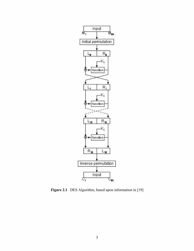
5
Figure 2.1 DES Algorithm, based upon information in [19]

6
Figure 2.2 DES Round, based upon information in [26]
Prior to starting the first round, the plain text is split into a left and a right side, 32 bits
each. The key for the encryption is first split into two 28 bit halves and then the halves
are circular shifted by one or two places depending on the round. After being shifted, 48
bits are selected via the compression permutation. The right side of the data being
encrypted, Ri-1, is the left part of the data for the next round, Li. The right side also goes
through a series of permutations, substitutions, and XORs to create the right side for the
next round. The following equations show the operations that take place in a round to
create the two halves of the data for the next round.
1
1 1( , )i i
i i i i
L RR L f R K
−
− −
== ⊗
(2.1)
The function that is part of the equation for the right side, 1( , )i if R K− , consists of the
expansion permutation, a XOR with the key for this round, Ki, S-Box substitutions, and a
P-Box Permutation. The expansion permutation expands the 32 bits of the right side by
repeating some of the bits. The XOR operation with the key produces a result of 48 bits
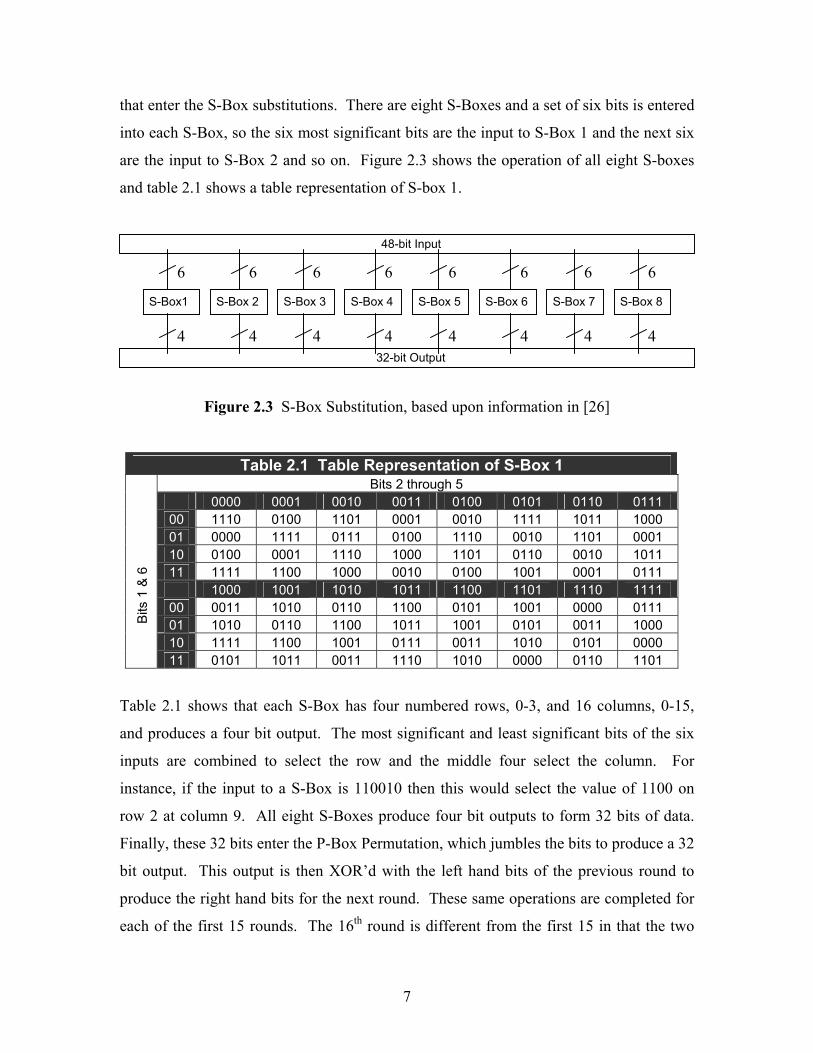
7
that enter the S-Box substitutions. There are eight S-Boxes and a set of six bits is entered
into each S-Box, so the six most significant bits are the input to S-Box 1 and the next six
are the input to S-Box 2 and so on. Figure 2.3 shows the operation of all eight S-boxes
and table 2.1 shows a table representation of S-box 1.
Figure 2.3 S-Box Substitution, based upon information in [26]
Table 2.1 Table Representation of S-Box 1 Bits 2 through 5
0000 0001 0010 0011 0100 0101 0110 0111 00 1110 0100 1101 0001 0010 1111 1011 1000 01 0000 1111 0111 0100 1110 0010 1101 0001 10 0100 0001 1110 1000 1101 0110 0010 1011 11 1111 1100 1000 0010 0100 1001 0001 0111 1000 1001 1010 1011 1100 1101 1110 1111
00 0011 1010 0110 1100 0101 1001 0000 0111 01 1010 0110 1100 1011 1001 0101 0011 1000 10 1111 1100 1001 0111 0011 1010 0101 0000
Bits
1 &
6
11 0101 1011 0011 1110 1010 0000 0110 1101
Table 2.1 shows that each S-Box has four numbered rows, 0-3, and 16 columns, 0-15,
and produces a four bit output. The most significant and least significant bits of the six
inputs are combined to select the row and the middle four select the column. For
instance, if the input to a S-Box is 110010 then this would select the value of 1100 on
row 2 at column 9. All eight S-Boxes produce four bit outputs to form 32 bits of data.
Finally, these 32 bits enter the P-Box Permutation, which jumbles the bits to produce a 32
bit output. This output is then XOR’d with the left hand bits of the previous round to
produce the right hand bits for the next round. These same operations are completed for
each of the first 15 rounds. The 16th round is different from the first 15 in that the two
48-bit Input
32-bit Output
S-Box1 S-Box 2 S-Box 3 S-Box 4 S-Box 5 S-Box 6 S-Box 7 S-Box 8
6 6 6 6 6 6 6 6
44 4444 4 4

8
sides of data are not swapped, as can be seen in Figure 2.1.
2.2 Differential Power Analysis
Differential power analysis (DPA) was announced by Kocher et al. in 1999 and has
become a hot topic of research. The method stems from timing attacks discussed in [16].
Timing attacks are able to discover information about the algorithm by observing the
time each operation takes [16]. DPA attacks belong to a family of attacks that try to
discover information about the key by examining the electronic consumption of a device
during the execution of a cryptographic computation [11]. Power analysis is considered a
passive attack because it is carried out by watching externally the interaction of the chip
with a possibly modified reader [27]. Smart cards can also be attacked using active
attacks, which are attacks where the chip is extracted, modified, probed, partially
destroyed, or used in an unusual environment. Active attacks rely on special knowledge
along with requiring the use of costly equipment [27, 12]. Since active attacks leave
clear signs of tampering, passive attacks are a much better approach in situations where
the attacker does not want anyone to know the card has been attacked [27]. Another
reason that the DPA attack is impressive is that the secret key can be discovered without
finding out anything about the particular implementation of the algorithm [11]. To
perform the entire DPA attack requires skills in statistics and cryptography for the attack,
as well as programming skills and experience in instrumentation to build up an automatic
measurement system and electronic skills to improve results [1].
Kocher et al. were also the first to discuss Simple Power Analysis (SPA), which is a
simpler derivative of DPA. SPA looks at the power trace and with a fine enough
resolution the attacker can draw conclusion as to which operations are being carried out
[29]. The typical attack on a Data Encryption Standard (DES) implementation on a smart
card shows a trace where the 16 rounds of the DES operation can easily be seen.
SPA is used to reveal a sequence of microprocessor instructions and can thus be used to

9
break cryptographic implementations in which the execution path depends on the data
being processed. There are particular operations that occur in cryptographic alogorithms
implemented in software that SPA can attack including the DES key schedule, DES
permutations, comparisons, multipliers, and exponentiators. In the case of DES
operations, conditional branches are usually the cause of significant power consumption
differences [17]. An exponentiator that computes binary exponentiation using the square
and multiply algorithm provides a good example of the usefulness of SPA. Consider, for
example, if the attacker sees the following operation order occur:
SMSSMSMSSSMSSSSM, where S and M stand for square and multiply operations,
respectively. From this information, the attacker could easily determine the key to be
10110010001 [29]. Although the above traces and examples show the effectiveness of
SPA, it can easily be defeated in software by avoiding such practices as a branch being
dependent of on some part of the secret key. In addition, the power variations of most
hardwired implementations of symmetric cryptographic algorithms are small enough that
SPA cannot yield any information about the key [17].
DPA builds on the SPA concept by combining power traces with a statistical approach.
DPA has roots in timing attacks that were first proposed in [16]. Timing attacks worked
because the systems implementing the cryptographic algorithms took differing amounts
of time depending on the inputs. Therefore, by studying the amount of time required to
perform operation of the secret key, the attackers are able to gleam information that could
enable them to break the cryptosystem [16]. The main concept behind DPA is to
correlate what is being seen on the power traces back to information about the key. The
reason the information can be easily correlated back to key information is that most
components today use CMOS gates, where the majority of power is dissipated when the
gates switch, commonly referred to as dynamic power [6].
Below is a description of a DPA attack on DES according to [17], [11], and [12]. An
attack on DES is being considered since DPA was first demonstrated against DES. In
this description, it will be assumed that the attacker knows the plaintext and is varying it.
This is commonly referred to as a known plaintext attack. First, the attacker performs

10
some number of encryption operations, N, varying the plaintext input for each iteration.
For each encryption, a power trace is recorded and saved for use later. In order to make
the power trace reasonable in size, the power is only recorded for the part of the
algorithm that the attacker is interested in. For a known plaintext attack the part to
concentrate on is the first round. Each plaintext input will be referred to as PTi where i is
equal to one to N and each power trace will be labeled Pi where Pij is the point on power
trace Pi at time j. Once the attacker has acquired N traces, the average power is
calculated. This is done by calculating the average power at each point in time j using the
equation below.
1
1 Nj i ij
P PN =
= ∑
(2.2)
Knowing the average value at every point in time the average trace can be constructed.
The next step is for the attacker to choose a target bit. A typical first choice is the first
output bit of the first S-Box of the first round of the DES algorithm. The value of this bit
will be referred to as b. This bit only depends on six bits of the secret key and bits from
the right side of the plaintext which is being varied by the attacker.
The attacker then makes a guess at the value of the six key bits that affect b. In statistical
terms this is referred to as forming a hypothesis, called H0. Once a guess has been made,
then the theoretical value of b can be determined for each of the N iterations. The power
traces are then split into two groups. The first group consists of power traces for which
the theoretical value of b is zero, P0, and the other group consists of traces for which the
value is one, P1.
The average power trace for the group in P0 is calculated using the following equation.
0 00
1 Nj iji
P PN =
= ∑ (2.3)

11
Once that is known, the attacker can statistically compare 0P to P using the t-test to
determine whether or not a correlation exists. If the choice of the key is incorrect, the
power traces will be uncorrelated and the statistical difference between the two will
approach zero. However, if key choice is correct then there will be statistical differences
in the traces. If the power traces are uncorrelated, then H0 is false and a new guess has to
be made for the six bits of the secret key and the process starts over. There are only 26
possible key combinations for bit b.
After the correct set of key bits is found, the attacker can move on to the second S-Box
and then continue to move through each of the S-Box until all 48 bits of the sub key are
discovered. The final eight bits of the secret key can be found by performing DPA on the
next round of the algorithm or simply by brute force. The speed of the attack can be
increased by attacking all four output bits of a S-Box at once. Equation 2.4 below gives a
value for how many traces are needed for a d bit attack assuming N traces are used for the
one bit attack.
2
1 )2(d
NNd
d∗
=−
(2.4)
Working through this equation for a four bit attacks shows that it requires half the
number of samples as a one bit attack [20]. To perform the attack on the four output bits
of the S-Box, a hypothesis is formed about all four bits and the resulting traces are
grouped into sixteen categories. A comparison is made between the average of the traces
in the group corresponding to the hypothesis and the overall average with a spike
occurring in the differential trace when the guess is correct. DPA can be used to attack
Triple DES by first finding the outer key and then using it to decrypt the cipher text and
then attacking the next key.
The key to using DPA to attack other systems lies in the selection equation. For the DES
attack discussed above, the selection function focused on the first output bit of the first S-
Box of the first round. For AES, the attack is altered by concentrating the selection

12
function on the key scheduling part of the algorithm. This is a particularly good place to
focus on because the power at this point in the algorithm is only a function of the key and
not data [4]. Leaking during asymmetric operations, in cryptosystems such as RSA,
tends to be much larger compared to the leakage that occurs in symmetric systems [17].
RSA smart cards are vulnerable to DPA attacks and even SPA can reveal enough
characteristics of the RSA decryption to allow the attacker to recover the key [24]. The
selection function for DPA can be set up to test exponent bit guesses and determine
whether predicted intermediate values are correlated [17]. Also, since most RSA
implementations make use of the Chinese Remainder Theorem [24], the selection
equation can be centered on the reduction or recombination processes of the theorem
[17].
Since some countermeasures attempt to increase noise to make DPA tougher, a short
discussion of how noise affects the attack is presented here. During a DPA attack, more
noise means that the number of traces needed increases [12]. Noise reduction can play an
important role when trying to recover side channel information because signals sizes are
so small. Four basic types of noise exist in a DPA attack: external, intrinsic,
quantization, and algorithmic. Intrinsic, due to the random movement of charge carriers
within conducters, and quantization noise, due to the quantizer in the A/D convertor used
to sample the power, are small compared to the size of the side channel signals. External
noise can be reduced through careful use of the measuring equipment, good circuit
design, and filtering. This type of noise can be thought of as white noise and thus can be
removed using a matched filter. Finally, algorithmic noise is reduced through the
averaging that takes place during the DPA attack [21].
2.3 Countermeasures to DPA
This section discusses countermeasures that have been proposed in the literature since the
announcement of DPA. Most solutions proposed involve changes in software, and to
date very few have addressed solutions in hardware. Countermeasures will be discussed

13
in similar order to when they appeared in literature, with the exception that all software
proposals will be discussed first, followed by hardware proposals. A brief description of
each will be given along with tradeoffs of that idea or ways attackers can still recover the
side channel information.
The ideas of how to counteract DPA were first presented in [17], where the authors
roughly describe the characteristics of several categories of countermeasures. The first of
these categories includes approaches that attempt to reduce signal sizes. This is typically
attempted by using constant execution path code, choosing operations that leak less
information to the power trace, balancing Hamming weights, or by physical shielding
[17]. The idea of choosing operations that leak less information can be implemented by
replacing important assembler instructions by ones whose signature is tougher to analyze,
or reengineering important circuitry that carries out the arithmetic operations or memory
transfers. One solution that involves the balancing of Hamming weights is to have every
piece of data represented by itself and the inverse of itself combined, which requires
twice as much storage space. Also, for this to be successful, a register must be cleared
prior to each write or information can be leaked [29]. The reduction of signal sizes in any
of these ways typically cannot reduce the signal size to zero, and thus the attacker can
still discover information to perform DPA given enough traces [17]. For instance, in
[21], the authors discuss methods to remove noise to make reduced signal sizes easier to
detect. One possible exception is physical shielding, which if used aggressively can
make DPA attacks infeasible, but at the expense of both cost and space. Kocher et al.
also discussed countering a DPA attack by adding noise into the power trace [17]. Here
the main goal is to add enough random noise to make the attack infeasible, but to add
minimal overhead [20]. Special implementation techniques for hardware or software are
used to reduce the signal to noise ratio (SNR) to a level where the spikes from the DPA
analysis are hidden in the noise [12]. The best that can be hoped for with this method is
an increase in the number of samples required to accomplish the attack [17].
Random process interrupts (RPI) was one of the first proposed solutions. This idea stems
from the fact that power analysis attacks are possible because operations being attacked

14
occur at a constant place in time [21]. RPIs can be created in two ways, either by
introducing randomness into timing, or execution order [29]. Random timing shifts must
be introduced so that the computed means can no longer be correlated back to a particular
operation [11]. Timing shifts do not provide complete defense since an attacker can use
statistical techniques, such as cross correlation, to realign the power traces [29]. The
randomization of the execution order seems more likely to provide protection against
DPA attacks, but can cause other problems if not done carefully [17]. The basic idea of
randomizing execution order is that dummy instructions are randomly placed between
actual instructions so that the operation order from one encryption to another differs.
This desynchronization effect causes the spikes from the DPA selection function to
become smeared across consecutive cycles [8]. It is argued that this type of
countermeasure must be done extensively in order to be effective, but a mechanism that
would allow for aggressive randomization is not provided [29]. Even with extensive
randomization, Clavier et al. have developed an integration process to recover the spike.
They propose a sliding window DPA, which involves the integration of the samples over
which the spike has become smeared. The first step in the process is to perform a regular
DPA attack and develop the differential curve from the selection function. The second
step is the integration or the adding of the consecutive power values over the samples the
spike was smeared. The authors suggest thinking of this step in terms of a comb where
each tooth corresponds to a point on the differential trace. All the values pointed to by
the teeth of the comb are added to perform the integration. The number of extra cycles
required when randomization of execution order is employed, N’’, is given by Equation
2.5.
2''N k N= (2.5)
In the above equation, N is the number samples required to perform DPA on a circuit
where randomization is not used and k stands for the number of samples over which the
peak is spread. Using the integration technique, this number can be reduced to just k
more samples. Another equation for the number of samples needed is 2np, where p is the
probability with which RPIs happen and n is number of samples the peak is smeared

15
across [8]. The more exotic approach of randomizing the order in which the S-Boxes are
completed has been proposed, but this again requires extensive randomization which in
the case of S-Boxes causes performance penalties [12]. S-Box randomization can also be
undone using integration [7]. For the few cases where the algorithm is being
implemented on a threaded processor, random threads could be used to execute random
encryptions in hopes of masking data. The downside to this approach is that it increases
computational cost considerably [29].
This next set of countermeasures all strive to defeat DPA via altering the cryptographic
algorithm so the secret key is not used within the main operation. There are three types
of these countermeasures: balanced algorithm, information blinding, and information
splitting. For an algorithm to be considered balanced it must be designed so that all
operations only have a very slight dependence on the input data [29]. Information
blinding works on the premise that a new value is created by the combination of the
sensitive data with some random value in a reversible way. Examples of this include the
XOR of the values or the modular addition [21]. Information splitting consists of
splitting values into a number of other states [29]. An interesting implementation that is
uses information blinding and splitting to keep the data from the attacker is presented in
[11]. There the authors suggest that any intermediate value V that occurs in the process
of the algorithm that in some way depends on the input or output should be split in k
values in a way that V equals a function of these k values. There are two conditions that
must be met in order for this process to mask the value of V. First, knowing one of the k
V values does not allow the attacker to determine information about the other values or V
itself. Secondly, the function that recombines the k values is such that any value
performed on V can be performed on the k values individually.
For the DES algorithm, the authors propose simply creating two V values where the
recombination function is the XOR of the two values. This requires the reworking of all
operations that are carried out in the algorithm. These include permutation of the bits of
V, expansion of the bits of V, XOR of V with some value V’ of the same type, XOR
between V and a value depending on the key, and transformations of V using the S-

16
Boxes. For the first two operation mentioned above the same operation that was used on
V can know be used on the two V values, V1 and V2. Now for the third operation, both V1
and V1’ are XORed together along with both part twos and the XOR function can still be
used to recombine them. Then for the fourth operation either part one or two of V is
XORed with the valued derived from the key. The fifth operation involving the S-Boxes
is where things get complicated. It basically consists of creating the new S-Boxes that
take in 12 bits and produce 4 instead of the original which takes in 6 and produces 4.
This is also joined with a random function A to provide the new equation shown below
[11].
)),()(),,((),('),( 21212121'
2'
1 VVAVVSVVAVVSVV ⊗⊗== (2.6)
This will at least lead to a doubling in the computing resources needed, which is not
feasible [29]. Also, the author themselves admit that this method requires too much
storage space for the new S-Boxes and A functions. Some alternatives are proposed
which attempt to reduce the sized required by only requiring nine new S-boxes [11].
New research has also shown that the DPA attack can be adjusted to handle masking
[30]. Information blinding techniques appear to be more successful in systems where
exponentiation is part of the algorithm, but at the expense of computational time. Also,
the changes must be examined thoroughly to avoid causing other nonintended
weaknesses [17]. Since the S-Boxes are the heart of the algorithm and provide the
security [31], this could be where potential weaknesses that [17] warned about could be
introduced. S-Boxes were specially designed to prevent classic mathematical attacks and
changes in them could make the new system susceptible to these older attacks.
Other software countermeasures that have been suggested include using nonlinear key
updates where a hashing function is used on the key to attempt to destroy partial
information gathered by the attacker, and the use of key counters to keep attackers from
gathering a large number of samples [17]. Most software proposals are ad-hoc solutions
that are based upon simplistic techniques. The proposals miss the importance of this type
of attack and its underlying basis, and can be nullified by signal processing [7].
17
The threat of DPA stems from the fact that hardware leaks information during processing,
so a fundamental countermeasure would be to implement cryptographic algorithms in
hardware that either does not leak information or dissipates power in a random manner.
Despite this easily specified objective, hardware solutions are typically difficult to
design, analyze, and test [21]. Few hardware solutions have been proposed to this point;
the ones that have been proposed are discussed below. The hardware countermeasures
are grouped into two catogories: one where control on the input power to the chip is
implemented and one where the circuitry is changed to avoid the leaking of information.
Several techniques are presented in [27] that are part of the first category. One idea is to
control the input power using a sensor that will measure the actual power supplied to the
chip and then attempt to equalize it by controlling a current sink [27]. A problem with
this method is that the current change happens so rapidly that any compensation
technique is likely to lag behind [30]. Another solution along this line is to place a
capacitor across power supply lines to smooth the power consumption curve, but physical
limitations constrain the size of such a capacitor [27]. Any attempt to make the power
consumed by a smart card absolutely uniform by changing the physical design is
unsuccessful because sensitive digital oscilloscopes can capture any nonuniformity and
then that data can be analyzed to reveal useful information. Also, the attempt to cause
every instruction executed to switch the same number of gates is very unnatural and
requires twice as much area and total power consumption, along with slowing down the
operation of the card. Another method for controlling input power is to use an internal
battery to remove the external power pins. This would keep attackers from being able to
obtain power traces without tampering with the card. The downside is that batteries small
enough to fit onto a chip are expensive and have a short life span. It would not be
practical to have easy access to the battery because that would mean that a power trace
could easily be obtained and then the usefulness of the approach is circumvented. To
avoid having to replace the battery, it has been proposed to use rechargeable batteries.
The reader could be used to recharge them, but rechargeable batteries of this size cannot
hold a charge for long amounts of time and thus would have to be recharged at the

18
beginning of each use causing an unreasonable charging delay at each use. Also,
rechargeable batteries will wear out after relatively few charges and then must be
replaced [27].
Along the same lines, but without all the issues surrounding the battery on chip is the idea
proposed by [27] of decorrelating the power supply from a smart card by using capacitors
as power isolation elements. Figure 2.5 shows the configuration of this countermeasure.
Figure 2.4 Using capacitors as isolation elements, based upon information in [27]
The basic idea is that capacitor one (C1) is discharging and powering the chip while the
second capacitor (C2) is charged by the power supply and then the roles are reversed.
The cyclic process that is proposed is to first disconnect C1 from power supply and then
second connect C1 to chip. Thirdly, disconnect C2 from chip and fourthly connect C2 to
external power and continue the cycle. This setup means that the power supply is never
connected directly to the chip. Thus the supplied current is uniform while the power used
by the chip is still irregular. Also diodes are used to avoid any leakage current when both
capacitors are connected to the chip. The author recommends using a 1 uF capacitor and
also discusses ways the capacitors can be embedded in to the smart chip while claiming
only the addition of a few cents to the overall cost of the smart card. Instead of using a
time limit or voltage level for when the capacitors should switch it should be triggered by
a fixed number of instructions. One issue that still remains is that an attacker can still
infer the power consumed by the chip during discharging period, which determines the

19
initial current at the beginning of the next charging cycle. This information leakage can
be reduced in two ways: firstly making the discharging cycle as long as possible and
secondly using new circuitry that discharges the capacitor to a fixed value after it is
disconnected from the chip so that it always has to be charged the same amount.
Capacitors have several advantages to on-chip batteries including being smaller and
cheaper than batteries. Also, capacitors can be recharged an unlimited number of times,
have no memory effects, and can be recharged in a fraction of second, all qualities that
are disadvantages of batteries. Since the capacitor can only hold charge for about 100
instructions to complete, they must be recharged continually to complete long tasks, but
this should not have adverse effects on the operation of the chip [27]. Unfortunately, as
with batteries, capacitors are still size prohibitive when it comes to placing them on chips
[30].
The most recent hardware countermeasure proposed is by [30]. The authors claim that
software countermeasures attack the problem at the algorithmic level and power- related
countermeasures attack the problem at the architectural level, while the issues related to
DPA originate at the logic level. The main idea behind this proposal is that the simplest
solution to DPA is to have the encryption module or at least the sensitive parts of it
implemented in a logic family that has power consumption independent of the signal
transitions. To do this, the proposal is to implement items in a logic family that combines
differential and dynamic logic. In differential logic, the attacker can differ between 0-
1/1-0 transitions and 0-0/1-1 transitions because power is only consumed during the first
two transitions. On the other hand, in dynamic logic, one can differentiate between 0-
1/1-1 transitions and 0-0/1-0 transitions since only the first two consume power. In
Figure 2.5, a generic form of both of these logic types along with their power
characteristics in a truth table form is presented. For this figure, the gray areas represent
the transitions that consume power.

20
Figure 2.5 Power characteristics in Truth Table form for Differntial Logic (left) and
Dynamic Logic (right), based on information in [30]
Consequently, neither of these types of logic styles by themselves will resist DPA. The
idea of [30] is to combine the two together along with sense amplifier technology so that
none of the four transitions can be differentiated from the others. The authors label this
as Sense Amplifier Based Logic (SABL).
While it is true that the output transitions will offset each other, the capacitance driven by
the outputs must also be matched. According to the authors, this proposal requires about
twice as much space and energy than a standard CMOS implementation [30]. Another
issue is that since SABL has the precharge element of dynamic logic, certain limitations
apply to how many gates can be cascaded together. Cascading has to be done by either
inserting an inverter between each gate or by alternating gates with n pull-down networks
with gates having p pull-up networks. The use of inverters limits the number of gates
that can be cascaded together to the number that can evaluate in one clock period and
only noninverting logic can be used [33]. The second alternative eliminates the
Pull-up Network
inputs
Pull-down Network
inputs
out out
VDD
Pull-downNetwork
inputs
Evaluation Stage
out
VD
Precharge Stage
ini ini+1 outi outi+1 outi outi+1 ini ini+1 outEv outPr
0 1 1 0 0 1 0 1 0 11 0 0 1 1 0 1 0 1 10 0 1 1 0 0 0 0 1 11 1 0 0 1 1 1 1 0 1
n
n n

21
disadvantages of the first, but the speed of the circuit will be degraded because of the
mobility of holes in the p transistor gates [25]. Finally, the use dynamic circuits requires
extra design effort to ensure correct operation under all circuit conditions including
timing sequences, charge leakage, and noise sensitivity [33].

22
Chapter 3 – Experimental Framework
This chapter discusses the DES core that was used for experiments in this project. The
coding of the DES algorithm will be examined along with the test procedure to prove the
core works correctly. The chapter then explains changes that were made to the core and
why they were needed. The chapter concludes with a description of the tool that was
created to instrument the synthesized code to count transitions and collect them in a
usable format.
Figure 3.1 Outline of Chapter 3
3.1 The DES Core and Test Verification
The DES core that is used throughout this project was developed by [15] and is
distributed free of charge. After examining the VHDL code and determining it would
work for needs of this project, the next step was to ensure code worked correctly. To
ensure correct operation of the algorithm it was tested using a known answer test from

23
[23]. In this test, the plaintext (PT) value in hexadecimal is 0000000000000000 and the
key, also in hexadecimal, is 10316E028C8F3B4A. Using this PT and key combination
produces a cipher text (CT) value of 82DCBAFBDEAB6602 in hexadecimal. The result
of this test with the DES core is presented in Figure A.1 of Appendix A. There it can be
seen that in fact the VHDL DES code does work correctly.
Changes made to the provided DES code were minimal and were only needed to facilitate
collection of data. Most changes were made to the test bench in order to ensure proper
timing. The VHDL DES code and its test bench after changes are presented in Figures
A.2 and A.3, respectively. The changes are marked by comment lines before and after
the changes describing why the changes were made. These changes have no effect on the
operation of the core, but are needed to control items added later that collect samples
while the DES algorithm is being processed.
The code for this core was written so that it could be instantiated in two ways, either with
the des_fast component or with the des_small component. For the purposes here
only the des_small component was used and thus items pertaining to the des_fast
component were removed prior to synthesizing. Next, the component declarations for
des_small and des_round are made. The component des_small involves the input
and output ports for the system, while des_round controls what feeds into and is received
from each of the 16 rounds in the DES algorithm. Next inside the package are function
declarations for the different parts of the algorithm. These parts include the initial
permutation, final permutation, key permutation, compression permutation, expansion
permutation, S-Box substitutions, P-Box permutation, and the key shift. For more
information on the operation of these items refer to Section 2.1 or [9].
Overall, the des_small entity controls the input and output of the system, the
des_round entity, and functions that occur outside the rounds. The des_round entity
controls the functions that occur within a DES round when activated by the des_small
entity. Once the code was understood and found to work correctly, the next step was to
synthesize the code. Finally, the synthesized VHDL model was simulated with the

24
original test bench to ensure that it worked correctly.
3.2 Finding Nodes of Interest
In the case of an FPGA with synthesized DES code being loaded into it, every transition
of a signal can possibly leak information through side channels. This section explains
how to determine which signals should be examined and how to locate these important
signals. The architecture of an FPGA causes the leakage of some signals to be much
more prevalent on a power trace. The general architecture of a Xilinx FPGA consists of
many blocks of logic or combinational logic blocks (CLB) connected together. Figure
3.2 shows the positioning of CLBs in a Spartan II FPGA with interconnects running
between them.
Figure 3.2 Block Diagram of Spartan II, based upon information in [34]

25
The signals that are the output of CLBs are the signals most likely to leak information at
a level that would affect the power trace. As will be explained shortly, the signals
internal to the CLB dissipate much less power than the output signals. Thus, since a DPA
attack is conducted on the power dissipation of a circuit, these signals can be ignored. To
make this argument clear, a discussion of power in CMOS circuits is presented.
The equation for total power of a CMOS circuit is given by [Cha93].
ddleakageddscclkddLttotal VIVIVfVCpP ++= )( (3.1)
The first term in Equation 3.1 represents the dynamic component of power where pt is
probability that a power consuming transition occurs, CL is the load capacitance, V is the
voltage swing, Vdd is the supply voltage, and clkf is the clock frequency. The term pt is
also known as the activity factor of the circuit. The second term represents the direct-
path short circuit current Isc, which occurs when both the NMOS and PMOS transistors
are active at the same time causing a short circuit from power to ground. The final term
represents the power consumed through leakage current, Ileakage, which can arise from
substrate injection and subthreshold effects and is primarily determined by fabrication
technology considerations. In a well-designed circuit the dominant term is the dynamic
power, which is represented by the first term in Equation 3.1 and reproduced below
[Cha93].
)( VfVCpP clkddLtd = (3.2)
In most CMOS circuits, the voltage swing is equal to Vdd, so the supply voltage is just
squared [Cha93]. The two factors that are important to DPA, transitions and capacitance,
are found in Equation 3.2. The factors pt and fclk both play a part in the transitions of the
circuit. In some texts, [25] and [33] for example, the equation for dynamic power is
stated as shown below.

26
2d L ddP C V f= (3.3)
For this equation, f stands for the number of times the gate is switched on and off in a
second or the combination of pt and fclk. From Equation 3.3, it can be seen that for any
given signal in an FPGA that only f varies widely during execution. For the case of a
configured FPGA, Vdd and CL are constant for a given node. The CL term is the effective
capacitance seen by the gate. In the case of a CLB output, this value consists of the
capacitance of interconnects it crosses and the gates driven. Since the capacitance of
each node is not known, but constant, the power of any signal can be estimated from its
transition count [22]. This allows the dynamic power to be estimated without the need of
a transistor level model or schematic. If the capacitance of each node were known, then
it could be used to weight the equation to better estimate power consumption.
In [28], the authors study the dynamic power consumed by a Xilinx Virtex II FPGA by
isolating different resources and finding their effective capacitance. Table 3.1 shows the
effective capacitance found by [28] for FPGA components.
Table 3.1 Effective capacitance summery Type Resource Capacitance (pF)
Ixbar 9.44 Interconnect Oxbar 5.12
per CLB Double 13.20 Hex 18.40 Long 26.10
Logic LUT inputs 26.40 per CLB FF inputs 2.88
Carry 2.68 Clocking Global wiring 300
Local 0.72
The results in Table 3.1 show that, other than global wiring for clocking, the resources
with the largest effective capacitance are inputs to LUTs. The components with the
second highest effective capacitance are interconnects. There are several types of
interconnects in an FPGA, but all have a high effective capacitance [28]. Although the
capacitance values were found for a Xilinx Virtex II FPGA, it is assumed that the relative

27
ordering of component capacitances is the same for the Spartan II architecture used here,
since both have very similar CLBs and interconnect components.
To verify this statement, the Standard Delay Format (SDF) file for the synthesized code
of the DES core was examined. The SDF file is part of the IEEE VITAL simulation
process. This file is created by the place and route tool and represents the back annotated
delay of each component. For each input to a gate in the circuit, an input and output
delay is given. The input delay represents the delay seen by a signal driving that input
due to capacitance along that wire. The ouput delay models the internal delay of the
component. In examining the SDF file for the synthesized DES core, the input delay to a
X_BUF component representing X or Y output was not specified, meaning that the
default value of 0 ns was used. The inputs to flip-flops driven by internal CLB circuitry
have a delay of 0.496 ns. Finally, the delay of LUT components was typically in the
range of 1.5 to 3 ns, with some values over 4 ns. These findings show a correspondence
between the effective capacitance found for the Virtex II family and the Spartan II device
used here. Thus, since LUTs are driven by either input ports or outputs of CLBs, these
results show that CLB outputs drive much larger capacitive loads then any of the signals
internal to the CLB. Consequently, the switching of CLB outputs will have a much
larger impact on the power trace found during processing. Thus, the internal signals are
assumed to be negligible for this discussion and the focus will be on the CLB outputs.
Given the argument that the outputs of CLBs are the most heavily loaded signals, the
correlation between power consumption and bits of the key can be estimated by finding
the correlation between transitions on CLB outputs and bits of the key. To do this, the
synthesized VHDL code was instrumented to find this correlation. The first step was to
determine how the outputs of CLBs are labeled in the synthesized file. Since each FPGA
family uses different naming conventions, this step must be done anytime the target
FPGA family is changed. One way of determining the naming conventions for a
particular family is to open the FPGA map generated by the Xilinx synthesis tool and
examine it using FPGA editor, which is part of the Xilinx ISE. The map file displays
how the tool placed the synthesized code onto the FPGA. Once in the editor, the outputs

28
of multiple CLBs can be explored to find the signal names. These signal names can then
be searched for in the synthesized VHDL code to determine which component produced
them. For instance, some signals will be the output of flip-flops, which are the X_FF
components in the Xilinx Spartan II family. Knowing the components from which CLB
outputs are produced is the first step, but these components can possibly be used for other
signals in the FPGA and must be inspected. If they are used for signals other than CLB
outputs then observing the name given to the components can usually differentiate the
outputs of CLBs from other signals. To make this discussion clear, Figure 3.3 shows the
declaration of two buffer components.
round0_N1730_XUSED : X_BUF XUSED means CLB output port map ( I => round0_N1730_F5MUX, O => round0_N1730 ); dout_0_OBUF : X_BUF X_BUF here is not CLB output port map ( I => dout_0_OUTMUX, O => dout_0_OUTBUF_GTS_TRI );
Figure 3.3 Instantiation of two buffer components
In Figure 3.3, the first buffer serves as an output of a CLB for the Spartan II FPGA
family. The second, however, is not an output of a CLB. The buffer component is used
with signals other than CLB outputs but its name signifies it as a CLB output. The
component name is the alphanumeric characters given before the colon. In this family, a
component name that ends in XUSED is the X output of a CLB. The architecture of a
CLB will be discussed further in Chapter 4. See Figure 4.14 for a diagram of a Xilinx
Spartan II CLB.
Once the names of CLB output components are known, the next step is to collect all the
signals that are outputs of these components. The C++ code that was used to find the
nodes of importance along with other operations is listed in Figure A.4.

29
Figure 3.4 Flow of C++ Code synth2test.cpp
The flow of this C++ code is shown in Figure 3.4. The code has three inputs: the
synthesized VHDL file, a file named nodes.txt, and a file named port.txt. The
code reads the file nodes.txt to determine the component types that are important. This
file makes the code adaptable for different families of FPGAs. The C++ code reads in a
line of the synthesized code and compares it to all the lines of the nodes.txt file.
When a match is found the output of that component is saved as an important signal for
use later. When other FPGAs are used, the only thing that needs to be altered is contents
of the file nodes.txt. If this code was run consistently on different families then the code
could be altered to request the user to enter the family being used and use that response to
choose the file that matches the family used. The ports.txt file is used to signify
which port that the code needs to use when setting up the count process. This port is
always set to key_in here, but for another version of DES VHDL code it might need to
be changed if the key input port has a different name. For this VHDL DES core, there
are 889 CLB outputs found when it is synthesized to a Spartan II FPGA. Finally, the
C++ code produces the instrumented VHDL synthesized file, which is discussed further
in Section 3.3.
As discussed above, the transitions of the CLB output signals are important in finding a

30
correlation between the hardware and the key. To monitor these transitions, a new
process is created in the synthesized VHDL file. For each CLB output, two transition
counts are maintained for each bit of the key, one for when the bit is a zero and one for
when the bit is a one. With a 56 bit key, this creates 112 signals from one CLB output.
Finally, a total count signal is created to keep track of all transitions that occur to the
CLB output. Thus, 113 signals must be created for each CLB output.
The C++ code discussed above and presented in Figure A.4 of Appendix A instruments
the synthesized VHDL to create this process. After the first cycle through the file to find
the important signals, the next step was to cycle through the file a second time to add the
counting process to the VHDL file. As mentioned, for every important signal, 113 count
signals must be declared; this is the first step of the second cycle. Once the end of the file
is reached for the second time, the new process is created. Inside the process there is an
“if” statement used to increment each count signal. Figure 3.5 gives an example of one
of these “if” statements.
if (round0_N1718'event and key_in(55) = '0') then
ATRAN_round0_N1718_55bit0cnt <= ATRAN_round0_N1718_55bit0cnt + 1;
end if;
if (round0_N1718’event and key_in(55) = ‘1’) then
ATRAN_round0_N1718_55bit1cnt <= ATRAN_round0_N1718_55bit1cnt + 1;
end if;
Figure 3.5 Example of If Statement from New Process
The “if” clause is triggered by a transition on the CLB output and the bit of the key that
corresponds to the count signal. In this case, the CLB output is round0_N1718 and the
bit of the key that is of importance is 55. The naming convention used for these new
signals can also observed in Figure 3.5. A generic form of this naming convention is
ATRAN_<original signal name>_<bit #>bit<bit value>cnt. ATRAN is used at the
beginning to easily differentiate these signals from the others. As far as the suffix,
<bit #> represents the bit of the key that is observed by this count signal and <bit value>
31
signifies whether signal is looking for the bit of the key to be a one or zero. The “if”
statement in Figure 3.5 increments the count signal when an event occurs on the original
signal and the 55th bit of the key is a zero. The second “if” statement is the same except it
triggers when the 55th bit is a one. These are just two of the “if” statements of the 113
that correspond to the CLB output signal.
With 889 CLB outputs that must be observed and 113 signals created for each, this means
that over one hundred thousand signals are created for this new process. Trying to read
all the count values from a trace window is unrealistic so the VHDL code was also
modified to write to a file using the TEXTIO package of VHDL. This allows a file to be
opened, written to each time the process is triggered, and closed at the end of the process.
Writing to the file required the addition of several changes to the test bench, as was
mentioned earlier. The changes allowed the encryption entity to write to the file while
keeping the decryption entity from writing. Each time the process is triggered, the file is
overwritten so that at the end of simulation, the file only contains the final counts of each
signal. In order to perform the write operations above, a couple of new lines are needed
for each new signal so that every time the process is triggered the new count value is
written to the output file. Once the final outputs are written to the text file, the counts can
be analyzed using a mathematical software package such as Matlab.
As the need occurred, the C++ code was altered to create other output files. For instance,
it was used to create a file containing the count signal names in the order in which they
were created. Also, since the statistical tests described in Chapter 4 require the variance
of each count signal, the C++ was altered to create a VHDL process that would record a
count signal value after each encryption. In this process, each count signal counts
transitions from the time din_valid becomes high until dout_valid becomes high.
At the dout_valid signal, the value of each count signal is written to the file and then
cleared. This file was then used to find the variance of each count signal.

32
Chapter 4 Results and Analysis
This chapter presents the analysis of the transition count results recorded by the modified
VHDL file described in chapter 3. Figure 4.1 shows the outline of this chapter. As
mentioned, the modified VHDL file writes all results to a text file. These results are
examined by comparing the differences in counts. This chapter also describes how these
results can be analyzed statistically using the visual test or the t-test. After the signals
have been fully analyzed, ways of decorrelating the nodes from the secret key are
explored. This includes the specification and development of a decorrelation circuit for
outputs of flip-flops. The effects that glitches have on the results are then examined.
Finally, design changes that could lead to decorrelation of signals or could make
decorrelation hardware simpler are discussed.
Figure 4.1 Outline of Chapter 4

33
4.1 Count Results & Simple Analysis
Chapter 3 discussed how the output file is created from the VHDL code. Figure 4.2 is an
excerpt of the count results file after 1000 encryptions. The order of the results
corresponds to the order they were created by the C++ code used to edit the synthesized
VHDL code, which allows the count value to be matched with its signal name.
Current Outputs 20795 ATRAN_round0_N3690_0bit0cnt 20438 ATRAN_round0_N3690_0bit1cnt 20885 ATRAN_round0_N3690_1bit0cnt 20348 20952 20281 20802 20431 20802 20431 20791 20442
Figure 4.2 Excerpt of Count Results File
In Figure 4.2, the numbers represent the total transitions recorded by each count signal.
As can be seen in Figure 4.2, the first value is the count value for the
‘ATRAN_round0_N3690_0bit0cnt’ signal in the generic form ATRAN_<original signal
name>_<key bit #>bit<key bit value>cnt. This means the signal ‘round0_N3690’
transitioned 20795 times during encryptions when the zeroth bit of the key was zero. The
next number represents the transitions seen by the ‘ATRAN_round0_N3690_0bit1cnt’
signal and so on.
These values are then loaded into Matlab for analysis. Having the 113 count signals per
CLB output signal in the VHDL code allows each of the outputs to be analyzed in terms
of each bit of the key. The first step is to determine how large the average difference
over 1000 encryptions is between the <bit #>bit0cnt and <bit #>bit1cnt signals where the
bit number is the same for each. The larger the difference in these values the greater the

34
chance that they will be found to be statistically different in the statistical testing, which
will be described in Section 4.2.
Figure 4.3 is a sorted plot showing the average count difference between <bit #>bit0cnt
and <bit #>bit1cnt for every count signal over 1000 encryptions. Figure 4.3 shows only
49,784 difference values instead of the original 100,457 signals. This is because there is
only one point on the plot for every difference between the two versions of the signal
representing the same bit of the key. Thus, having 889 CLB outputs brings the number of
necessary points to 49,784.
Figure 4.3 Average Count Differences from Least to Greatest
As can be seen in Figure 4.3, the majority of the values are relatively small. It is not until
the points are well past 30,000 that the values begin increasing quickly. Figure 4.4 is the
same graph zoomed in to show points starting at 48,000. This plot shows the points
having the largest average count differences with much more detail.

35
Figure 4.4 Zoomed in Version of Figure 4.3
Figure 4.4 shows that most of the differences fall well below a value of 0.2. The first
difference value to exceed 0.1 is at point 47,605. The average count differences in group
A are more than twice as large as those in B. Group A contains 48 points while group B
contains 288 points. Figures 4.3 and 4.4 show that only a few points have a large average
difference in transitions between when the bit of the key is a 1 and a 0. Thus, only a
small fraction of the circuit will have to be modified to reduce the correlation between
power consumption and bits of the key.
To reinforce this point, consider the following data. The sum of differences over all the
count signals is 1,394,600 with an average count difference of 28.0128 over 1000
encryptions. Group A accounts for 3.46% of the differences, while group B accounts for
10.35%. Table 4.1 shows a comparison of how much of the total count difference can be
removed by decorrelating a certain percentage of the total difference values.

36
Table 4.1 Comparison of Count Differences # Difference Values % of Total Diff Values % of Total Count Diff
4046 8.1271% 50.4747% 12269 24.6445% 75.0200% 22383 44.9602% 90.2500%
This table shows that relatively few difference values can account for a large percentage
of the total count differences. For instance, just 4046 difference values of the 49,784
total values account for over 50% of the total count differences. The values required to
account for 75% and 90% percent of the total count differences are also presented.
4.2 Analysis Using Visual Test & T-test
While finding nodes whose count difference is large is instructive, it is also necessary to
ensure the difference in counts between the <bit #>bit0cnt and <bit #>bit1cnt signals are
statistically significant. To do this, statistical hypothesis testing is employed. A
hypothesis is typically tested with either the visual test or the t-test [13]. Before
proceeding to the analysis of the results, both of these statistical testing methods are
briefly described here based on descriptions in [13].
The t-test is used to determine whether two unpaired samples of data are significantly
different. It involves about seven calculations, which are described in [13], to make the
decision. In [1], the authors found that simply finding the mean difference between two
samples is sufficient for determining whether two samples are significantly different.
Despite this, all data for this project was statistically compared. The visual test is a
simpler alternative to the t-test. For the visual test, the confidence interval of each sample
is computed separately and can be found with the following equation [13].
confidence interval
−±=
nrvavaluetx )(
(4.1)
In the equation above, x is the mean of the sample, var is the sample variance, and n is
the number of elements in the sample. The t-value is found from a t-value table using the

37
percentage of confidence desired and the degrees of freedom. A confidence interval is
computed for both of the samples and then both are compared to produce one of the three
following cases:
Case 1. The confidence intervals do not overlap and thus the samples are
significantly different.
Case 2. The confidence intervals overlap to the point that the mean of one sample
is within the interval of the other sample and thus the samples are not
significantly different.
Case 3. The confidence intervals only slightly overlap and neither sample’s mean
falls within the other’s interval. In this case, no visual conclusion can be
drawn and the t-test is needed for determining if the difference in the
samples is significant.
Figure 4.5 shows the visual representation of each of the three cases that occur in a visual
test where the dot is the sample mean and the line represents the confidence interval.
Figure 4.5 Three Cases that Occur in a Visual Test, based upon information in [13]
For the most part, the visual test was used here for the first test because it requires fewer
calculations than the t-test. The t-test was employed to handle situations where the third
case of the visual test occurred. For all statistical testing below, a confidence factor of
99.5% was used. Given this background on the statistical testing techniques, the next
step is to use them to analyze the count results.
To perform the visual test, the average, variance, and confidence intervals were
calculated in Matlab using the output file of the instrumented VHDL code. Excerpts of
A
B
AB
A
B
Case 1 Case 2 Case 3
38
the Matlab code used are presented in Figure A.5 of Appendix A. Once the confidence
interval was known for each count signal, the next step was to determine how many of
the count comparisons fell into Case 1 or Case 3 of the visual test. It was found that 1267
of the 47,605 differences, about 2.5%, could be grouped into Case 1, meaning that the
count signal ending in <key bit #>bit0cnt was definitely statistically different from the
one ending in <key bit #>bit1cnt. 3340 more of the differences, or about 6.7%, fell into
Case 3, meaning that they had to be evaluated using the t-test to determine whether the
two signals were truly significantly different. This means that 42,998 differences (over
90%) were statistically insignificant. So if all the differences in Case 3 were found to
differ significantly, less than 10% would be statistically different.
The t-test was employed to determine which of the count differences that fell into Case 3
were actually statistically different. The t-test showed that 3022 of the 3340 count
differences originally in Case 3 were statistically different. These, along with those in
Case 1 of the visual test, bring the total number of statistically significant count
differences to 4289, about 8.6% of the total count differences. The 1267 differences in
Case 1 are spread over 536 CLB outputs and the 3022 differences found with the t-test
are spread over the same outputs plus 116 more. Consequently, 652 CLB outputs are
correlated to bits of the key.
Next, the count results of these 652 CLB outputs will be investigated in several ways to
better understand their correlation to the key. It is important to note that the figures
presented in the rest of this section examine just the statistically significant count signals
and in terms of each of the 652 CLB outputs or bits of the key, while earlier Figures 4.3
and 4.4 showed all count signals individually.

39
Figure 4.6 Histogram of how many CLB outputs are correlated to each bit of the key
Figure 4.6 presents a histogram showing the number of CLB outputs that are correlated to
the different number of bits. From Figure 4.6 it can be seen that only a small portion of
the CLB outputs are correlated to more than ten bits of the key. Decorrelating less than
9.34% of the CLB outputs will remove over 25% of the correlations. Futhermore, over
50% of the correlations can be removed by decorrelating 24.3% of the CLB outputs.
Figure 4.7 shows a histogram of the number of the 652 CLB outputs that have a sum of
mean difference of statistically significant count differences in each of the ranges. Figure
4.7 shows that relatively few nodes account for a large portion of the mean differences.
To account for more than 50% of the mean differences, 167 CLB outputs or 18.79% of
the total must be decorrelated. The decorrelation of 44.43% of the total outputs will
remove over 80% of the mean differences. Figures 4.6 and 4.7 show that significant
improvement can be made by decorrelating only a small fraction of the CLB outputs.
Futhermore, the designer can trade off the amount of space required for decorrelation
versus the amount of decorrelation that is desired.

40
Figure 4.7 Histogram of CLB outputs with a mean difference of statistically significant
count differences in each range
Next, the correlation of each bit of the key is further investigated. Figure 4.8 shows the
sum of mean difference of statistically significant count differences per bit of the key. In
Figure 4.8, it can be seen that the sum of mean differences for each bit of the key is
relatively equal.
Figure 4.8 Sum of mean difference of statistically significant count differences per bit of
the key

41
To make this point further, Figure 4.9 presents the data in the form of a histogram.
Figure 4.9 confirms the conclusion from Figure 4.8 that all bits of the key have relatively
the same sum of mean differences. Athough one bit of the key has a slightly higher sum,
overall each bit of the key has about the same sum of mean differences of statistically
significant count differences that are correlated to them. Ways of decorrelating CLB
outputs are explored in the next two sections.
Figure 4.9 Histogram of the number of bits of the key that have a sum of mean
difference of statistically significant count differences in each of the ranges
4.3 A Decorrelation Circuit
During the DPA discussion in Section 2.2, it was explained that six bits of the key are
guessed as part of the attack. The size of the spike on a DPA trace is determined by the
voltage difference seen across a small resistor connecting the ground pin of the chip and
true ground as shown in Figure 4.10 [21].

42
Figure 4.10 Resistor Connected between VSS pin and True Ground, based upon
information in [21]
In summary, DPA requires the attacker to detect that voltage difference while it is
embedded in noise [21]. Reducing the number of count signal differences for any
particular bit of the key means fewer signals are correlated to it. Assuming the
capacitance driven by each output signal is approximately the same, all signals correlated
to a certain bit of the key provide an equal portion of the voltage difference that occurs.
Thus, by lowering the number of signals correlated to each bit of the key, the size of the
DPA spike will be decreased. The lower the signal-to-noise ratio, the more samples that
are required to detect the spike [21]. Equation 4.2, taken from [8], shows the relationship
between the voltage difference and the number of samples required to successfully
complete a DPA attack:
voltage differenceNσ
> (4.2)
In Equation 4.2, σ represents the noise and N is the number of samples necessary to find
the voltage difference in the noise. The inequality in Equation 4.2 shows that, as the
voltage difference decreases, the number of the samples required increases. Thus, the
reduction of counts signals causes the DPA spike to shrink and requires the attacker to
collect more samples. For example, if the size of the DPA spike were cut in half by
reducing the correlation, then the attacker would require four times as many samples to
complete the attack. According to [17], the best that can be hoped for with any
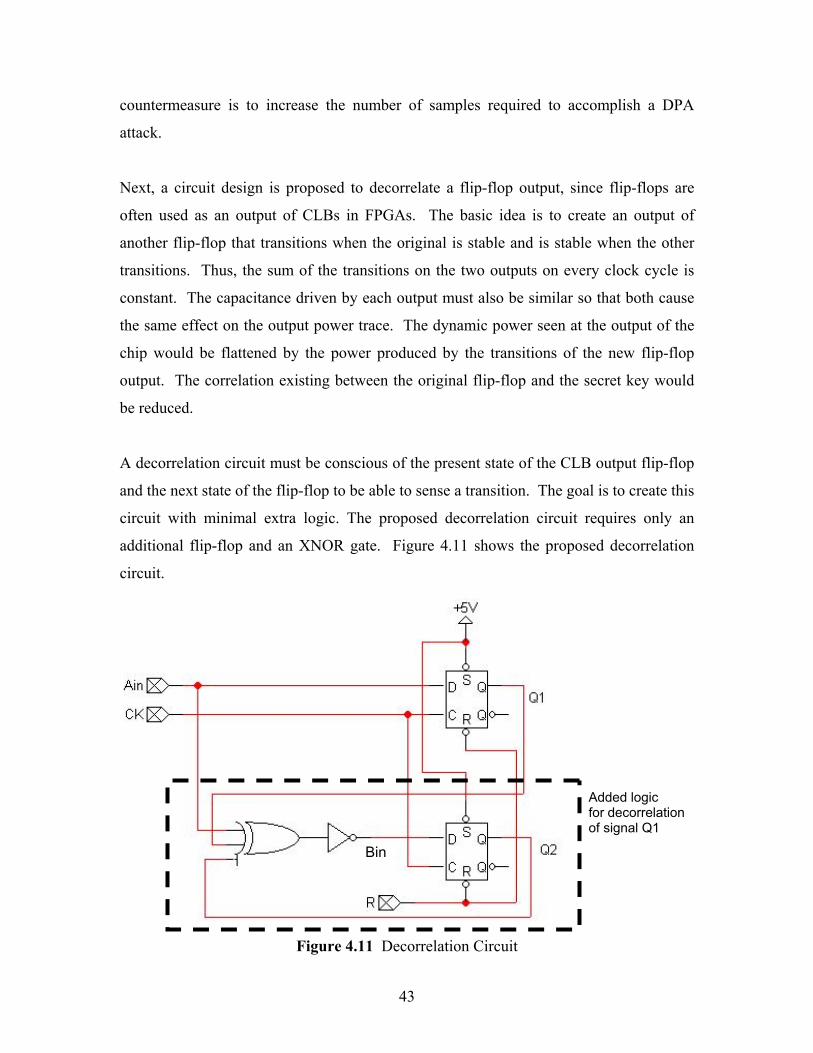
43
countermeasure is to increase the number of samples required to accomplish a DPA
attack.
Next, a circuit design is proposed to decorrelate a flip-flop output, since flip-flops are
often used as an output of CLBs in FPGAs. The basic idea is to create an output of
another flip-flop that transitions when the original is stable and is stable when the other
transitions. Thus, the sum of the transitions on the two outputs on every clock cycle is
constant. The capacitance driven by each output must also be similar so that both cause
the same effect on the output power trace. The dynamic power seen at the output of the
chip would be flattened by the power produced by the transitions of the new flip-flop
output. The correlation existing between the original flip-flop and the secret key would
be reduced.
A decorrelation circuit must be conscious of the present state of the CLB output flip-flop
and the next state of the flip-flop to be able to sense a transition. The goal is to create this
circuit with minimal extra logic. The proposed decorrelation circuit requires only an
additional flip-flop and an XNOR gate. Figure 4.11 shows the proposed decorrelation
circuit.
Figure 4.11 Decorrelation Circuit
Bin
Added logic for decorrelationof signal Q1

44
The top flip-flop in Figure 4.11 represents the original flip-flop output of a CLB. The
gates that form the decorrelation circuit are enclosed in the dashed line. Note that a 3-
input XOR gate in combination with an inverter is used to represent a 3-input XNOR gate
due to the absence of a 3-input XNOR gate in the target technology. The three inputs to
the XNOR gate are Ain, Q1, and Q2 and the output is Bin.
Table 4.2 XNOR Truth TableAin Q1 Q2 Bin 0 0 0 1 0 0 1 0 0 1 0 0 0 1 1 1 1 0 0 0 1 0 1 1 1 1 0 1 1 1 1 0
Table 4.2 shows the truth table for Bin. When Ain and Q1 are different the Q2 input will
be passed to Bin, causing the output of the new flip-flop to remain the same. On the
other hand, if Ain and Q1 are the same value then Bin becomes the inverse of Q2 and the
output of the new flip-flop toggles. The decorrelation circuit was tested to verify its
functionality and the results are presented in the Figure 4.12.
Figure 4.12 Output of Test on Decorrelation Circuit
Figure 4.12 shows the operation of the circuit. Exactly one of either Q1 or Q2 transitions
on every clock cycle. Thus, the two circuit outputs Q1 and Q2 will exhibit a constant
amount of switching and will not be correlated to the key.
Given this circuit, the next step is to determine the procedure for implementing it in the
synthesized VHDL code. This is accomplished by simply adding the component
declarations for the logic of Figure 4.11. Figure 4.13 is an excerpt of VHDL code

45
showing how the two new components can be added.
Test_FF : X_FF declaration of new decorrelation flip-flop port map ( I => TEST_INV_OUT, CE => VCC, CLK => clk_BUFGP, SET => GND, RST => round0_dout_11_FFX_ASYNC_FF_GSR_OR, O => TEST_FF_OUT ); Test_XOR3 : X_XOR3 declaration of new 3 input XOR gate port map ( I0 => TEST_FF_OUT, I1 => HOLD_FF_OUT, --state_3, I2 => round0_N3690, --N604, O => XOR3_OUT ); Test_INV : X_INV declaration of new inverter port map ( I => XOR3_OUT, O => TEST_INV_OUT ); Figure 4.13 Excerpt showing new VHDL code needed to create a Decorrelation Circuit
There are three components used to create the decorrelation circuit. The inverter is
needed because the SIMPRIM library does not contain XNOR gates. It would be the
hope that this new circuitry could eventually be integrated into a CLB. Since each
decorrelation circuit requires two gates and a flip-flop, the decorrelation of all 654 CLB
outputs found above to be statistically significant would require 1308 gates and 654 flip-
flops.
Despite the promising nature of a decorrelation circuit, there is one underlying factor that
currently makes it an incomplete solution to DPA. The majority of the signals that are
found to be significantly different do not leave the CLB through either of the two flip-
flop outputs, but through one of the two outputs that are not latched. The unlatched
outputs referred to here are the X and Y outputs shown in Figure 4.14. Only 63 of the
654 statistically significant CLB outputs, about 9.63%, could be decorrelated with this
circuitry. The 63 flip-flop CLB outputs only account for 2.63% of the total mean
difference of statistically significant count differences.

46
Figure 4.14 Basic Xilinx Spartan II CLB Circuitry, based upon information in [34]
One possibility is that the large count differences found in the unlatched outputs could be
attributed to the glitches occurring on these signals. The effect of glitches will be
examined in the next section.
4.4 Glitches and Filtering
Glitches occur on many of the important signals that are not the outputs of flip-flops.
Each signal typically has many glitches formed by some combination of static and
dynamic hazards. Static hazards occur when a signal undergoes a momentary change
when it should remain unchanged. A dyanamic hazard, on the other hand, is defined as
when a signal changes more than once when it is expected to make a single transition
[14]. Figure 4.15 shows static hazards, while Figure 4.16 shows dynamic hazards.
Figure 4.15 Plot showing Static Hazards occurring on two CLB outputs

47
Figure 4.16 Plot showing a Dynamic Hazard occurring on a CLB output
In Figures 4.15 and 4.16, the signals represented are the clock signal and two CLB
outputs along with their respective count signals. The two outputs shown were chosen
because each had a fairly high transition count and one is the X output of a CLB while
the other is a Y output. In Figure 4.15, the N1272 signal is seen to have one static glitch
while the round0_N3690 signal can be seen having two. Note that both static glitches
occur on the second signal within one nanosecond. In Figure 4.16, a dynamic hazard can
be seen on the second signal and again the entire glitch takes place well within one
nanosecond. During each of these hazards the count signals in each of the plots are
recording every transition. This raises the question of if the glitches were removed from
the signal would this effect which signals were found to be significantly different and
which have the highest number of transitions per encryption.
To explore this question, the VHDL count process was revised to filter glitches on CLB
outputs from the count signals. This was done by changing the conditions that trigger the
“if” statements. Figure 4.17 presents an excerpt of the process showing the altered “if”
statements.
if (round0_N959'delayed(1.1 ns)'event and key_in(37) = '0' and go = 1 and round0_N959'delayed(2 ns) /= round0_N959 and round0_N959'stable(1 ns)) then ATRAN_round0_N959_37bit0cnt <= ATRAN_round0_N959_37bit0cnt + 1; end if; if (round0_N959'delayed(1.1 ns)'event and key_in(37) = '1' and go = 1 and round0_N959'delayed(2 ns) /= round0_N959 and round0_N959'stable(1 ns)) then
ATRAN_round0_N959_37bit1cnt <= ATRAN_round0_N959_37bit1cnt + 1; end if;
Figure 4.17 Excerpt Showing Code Used to Filter Glitches

48
In Figure 4.17, each “if” statement now consists of five conditions. The two concerning
the key_in and go value are left from the original code. The first new condition is that
instead of just checking the signal for a transition, now the signal delayed by 1.1 ns is
monitored for new transitions. The second new condition is the comparison of the value
of the signal delayed 2 ns to that of the original signal to ensure a change actually occurs.
Finally, the signal is checked to ensure it has been stable for 1 ns ensuring that glitches
have not occur over the last nanosecond. These three conditions work together to ensure
that neither static nor dynamic hazards are able to affect the count signal.
The new transition count signals with filtering in place were collected and analyzed using
the visual test. For this new data the number of count signals that were found to be in
Case 1 was 895, and the number of count signals that were found to be in Case 3 was
3143. Using the t-test to analyze the difference values in Case 3 reduced the number of
statistically significant count signals to 2918. Table 4.3 compares the values found with
and without filtering of glitches.
Table 4.3 Comparison of Results With and Without Filtering Without Filtering With Filtering
Cnt Signal Differences in Case 1 1267 895 FF Signals in Case 1 3 3
Cnt Signal Differences in Case 3 3340 3143 FF Signals in Case 3 63 63 Total CLB Outputs 654 653
Case 3 Cnt Signal Differences After T-test 3022 2918 FF Signals After the T-test 63 63
Total CLB Outputs After T-test 652 652
As can be seen in table 4.3, filtering the glitches lowered the number of count signal
differences in each of the cases. Figure 4.18 is similar to Figure 4.7, a histrogram of
mean differences, after filtering to confirm the values found in Table 4.3.

49
Figure 4.18 Histogram of CLB outputs with a mean difference of statistically significant
count differences in each range after filtering
Figure 4.18 shows that the statistically significant count differences have been reduced
because the mean difference of these differences are all under five, whereas in Figure 4.7
CLB outputs had values ranging up to 13. In fact, the sum of mean difference of
statistically significant count differences in Figure 4.18 is a 41.5% reduction from those
in Figure 4.7.
Although the number of count differences were reduced, Table 4.3 and Figure 4.18 show
that the number of CLB outputs correlated to the key was not. Despite this, filtering still
produced positive results. As discussed in Section 4.3, the removal count signals
differences for any bit of the key will reduce corresponding DPA bias spikes, thus
requiring more samples to be taken during an attack. With about a 11% reduction from
filtering the voltage spike is also reduced about 11%, which would require about 26.25%
more samples to be taken to successfully complete a DPA attack.

50
The discussion of glitches here has examined the occurrence of glitches for one particular
set of parameters. Many parameters, including temperature, voltage, aging effect, and
fabrication variations, can have an effect on timing within a circuit. Changes in timing
will impact the amount of glitches that occur. Consequently, to better understand the
effect that glitches have on power analysis attacks, the circuit should be simulated across
the full range of the above parameters.
There are several techniques that can be used to combat the problems discussed above.
The first would be a redesign of the logic using some of the design techniques that
remove glitches. This was shown above to slightly reduce the number of count signal
differences found significantly different. Secondly, the basic circuitry, including CLBs
and interconnects, could be redesigned so that all CLB outputs are latched and drive
similar capacitance. This would eliminate glitches and make the decorrelation circuit
discussed above applicable to all CLB outputs. Finally, the CLB outputs that are found
to have significant correlation to the secret key could be traced back to their counterparts
in the VHDL behavioral code. This would allow the important parts of the behavioral
code to be rewritten in a way that these signals would become the outputs of flip-flops,
and then the decorrelation circuit of Section 4.3 could be employed to decorrelate the
switching of the signals.

51
Chapter 5 – Conclusions
This chapter summarizes the work in the thesis and presents directions for further
research.
5.1 Summary of Results
The focus of this thesis was two fold. The first goal was to develop a tool for
investigating power analysis attacks on synthesized VHDL models without the use of
transistor level models or schematics. The second was to explore countermeasures that
might be used on FPGAs. A summary of the results is presented below.
A tool was developed in Chapter 3 to analyze power in a FPGA. The transitions of CLB
output signals were used to estimate power and stored for analysis later. The tool created
instrumented VHDL code to collect statistics for further analysis. The design of the tool
allows for easy portability to other FPGA architecture families and behavioral code.
Using the tool described in Chapter 3, it was found that only a few nodes in the circuit
have a high correlation to bits of the key. This means that modifying only a small portion
of the circuit could dramatically increase the difficulty of mounting a DPA attack on the
hardware. Further investigation of the correlation between CLB outputs and the key
showed that a tradeoff exists between the amount of space required for decorrelation
versus the amount of decorrelation that is desired. Filtering of glitches on CLB output
signals proved to be successful in reducing the amount of correlation each CLB had.
Finally, a decorrelation circuit was proposed and shown to be successful at decorrelating
flip-flop outputs of a CLB, but can be used with only 9.66% of statistically significant
CLB outputs
.

52
5.2 Future Work
Several possible extensions to this work are proposed here. First would be determining a
method to match synthesized VHDL signals to their behavioral counterparts. This would
be useful for finding the behavioral code that could be modified to affect the CLB outputs
that are correlated to the key. Secondly, following along this same line of thought,
different types of changes could to be made to the behavioral code to see their effect on
the count results. These changes include design techniques to eliminate glitches and
using VHDL to infer latches for the signals of concern. Thirdly, an investigation could
be conducted in to changes made to the chip design, including CLBs and interconnects,
that would eliminate correlation between CLB outputs and the key. These changes could
consist of altering the CLB to cause all outputs to be latched, developing internal
circuitry to create decorrelation outputs corresponding to the CLB outputs, or adding
special capacitive loads that could be used to easily match the load capacitance driven by
the node it is intended to decorrelate.

53
References [1] M. Aigner and E. Oswald. Power Analysis Tutorial. [Online]. Availiable:
http://www.iaik. tugraz.at/aboutus/people/oswald/papers/dpa_tutorial.pdf, 2000. [2] E. Biham and A. Shamir, “Differential Cryptanalysis of DES-like
Cryptosystems,” Procceeding of Advances in Cryptography (CRYPTO ’90), 1990, pp. 2-21.
[3] E. Biham and A. Shamir, “Differential Fault Analysis of Secret Key
Cryptosystems,” Procceeding of Advances in Cryptography (CRYPTO ’97), 1997, pp. 513-525.
[4] E. Biham and A. Shamir, “Power Analysis of the Key Scheduling of the AES
Candidates,” The Second AES Conference, March 1999, pp. 115-121. [5] D. Boneh, R. A. Demillo, and R. J. Lipton, “On the Importance of Checking
Cryptographic Protocols for Faults,” Proceedings of Advances in Cryptography (Eurocrypt ’97), 1997, pp. 37-51.
[6] A. Chandrakasan, S. Sheng, and R. Brodersen, “Low-Power CMOS Digital
Design,” IEEE Journal of Solid-State Circuits, vol. 27, no. 4, pp. 473-484, April 1992
[7] S. Chari, C. Jutla, J. Rao, and P. Rohatgi, “Towards Sound Approaches to
Counteract Power-Analysis,” Proceedings of Advances in Cryptology (Crypto ’99), Lecture Notes in Computer Science, vol. 1666, 1999, pp. 252-263.
[8] C. Clavier, J. Coron, and N. Dabbous. “Differential Power Ananlysis in
the Presence of Hardware Countermeasures,” Proceedings of Cryptographic Hardware and Embedded Systems (CHES 2000), Lecture Notes in Computer Science, vol. 1965, 2000, pp. 252-263.
[9] Data Encryption Standard, National Bureau of Standards, U.S. Department of
Commerce, FIPS pub. 46, January 1977. [10] W. van Eck, “Electromagnetic Radiation from Video Display Units: An
Eavesdropping Risk,” Computers and Security, v. 4, pp. 269-286, 1985. [11] L. Goubin and J. Patarin, “DES and Differential Power Analysis,”
Proceedings of Cryptographic Hardware and Embedded Systems (CHES ’99),

54
Lecture Notes in Computer Science, vol. 1717, 1999, pp.158-172. [12] E. Hess, N. Janssen, B. Meyer, and T. Schutze, “Information Leakage Attacks
Against Smart Card Implementations of Cryptographic Algorithms and Countermeasures,” Proceedings of EUROSMART Security Conference, 2000, pp. 55-64.
[13] R. Jain, The Art of Computer Systems Performance Analsysis, Techniques for
Eperimental Design, Measurement, Simulation, and Modeling, New York: John Wiley & Sons, Inc., 1991.
[14] R. Katz, Contemporary Logic Design. New York: The Benjamin/Cummings
Publishing Company, Inc, 1992. [15] D. Kessner. (1999). VHDL DES Core. The Free IP Project. [Online].
Available: http://www.free-ip.com/DES/ [16] P. Kocher, “Timing Attacks on Implementation of Diffie-Hellman, RSA, DSS,
and Other Systems,” Proceedings of Advances in Cryptology (CRYPTO ’96), 1996, pp 104-113.
[17] P. Kocher, J. Jaffe, and B. Jun, “Differential Power Analysis,” Proceedings of
Advances in Cryptograpy (CRYPTO ’99), 1999, pp. 388-397. [18] M. Matsui, “Linear Cryptanalysis Method for DES Cipher,” Proceedings of
Advances in Cryptography (Eurocrypt ’93), 1993, pp. 386-397. [19] A. Menezes, P. van Oorschot, and S. Vanstone, Handbook of Applied
Cryptography. Boca Raton, FL: CRC Press, 1996. [20] T. Messerges, E. Dabbish, and R. Sloan, “Investigations of Power Analysis
Attacks on Smartcards,” Proceedings of USENIX Workship Smartcard Technology, May 1999, pp. 151-161.
[21] T. Messerges, E. Dabbish, and R. Sloan, “Examining Smart-Card Security under
the Threat of Power Analysis Attacks,” IEEE Transactions on Computers, Vol. 51, No. 5, pp. 541-552, May 2002.
[22] F. Najim, “A survey of power estimation techniques in VLSI circuits,” IEEE
Transaction on Very Large Scale Integration (VLSI) Systems, vol. 2, no. 4, pp. 446-455, December 1994
[23] S. Keller and M. Smid, “Modes of Operation Validation System: Requirements
and Procedures,” NIST Special Publication 800-17, February 1998. [24] R. Novak, “On the Security of RSA Capable Smart Cards,” Proceedings of the

55
10th Electrotechnical and Computer Science Conference, Vol. B, September, 2001, pp. 135-138.
[25] J. Rabaey, Digital Integrated Circuits. Upper Saddle River, NJ: Prentice Hall,
1996. [26] B. Schneier, Applied Cryptography Second Edition Protocols, Algorithms, and
Source Code in C. New York: Wiley, 1996. [27] A. Shamir, “Protecting Smart Cards from Passive Power Analysis with Detached
Power Supplies,” Proceedings of Cryptographic Hardware and Embedded Systems (CHES 2000), Lecture Notes in Computer Science, vol. 1965, August 2000, pp. 71-77.
[28] L. Shang, A. Kaviani, and K. Bathala, “Dynamic Power Consumption in Virtex II
FPGA Family,” Proceedings of the 2002 ACM/SIGDA Tenth International Symposium on Field-programmable gate arrays (FPGA ’02), February 2002, pp. 157-164.
[29] N. Smart, “Physical Side-Channel Attacks on Cryptographic Systems,” Software
Focus, Vol. 1, Issue 2, pp. 6-13, December 2000. [30] K. Tiri, M. Akmal, and I. Verbauwhede, “A Dynamic and Differential CMOS
Logic with Signal Independent Power Consumption to Withstand Differential Power Analysis on Smart Cards,” 29th European Solid-State Circuits Conference (ESSCIRC 2002), September 2002, pp. 403-406.
[31] W. Trappe and L. Washington, Introduction to Crytopgraphy with Coding
Theory. Upper Saddle River, NJ: Prentice Hall, 2002. [32] P. Wayner. (1998, June). Code Breaker Cracks Smart Cards’ Digital Safe. New
York Times. [Online]. Available: http://www.nytimes.com/library/tech/98/06 /biztech/articles/22card.html.
[33] N. Weste and K. Eshraghian, Principles of CMOS VLSI Design, A Systems
Perpective: Boston, MA: Addison Wesley Longman, 1993 [34] Xilinx. (2001, March). Spartan II 2.5V FPGA Family: A Functional
Description, Product Specification. Xilinx, Inc. [Online]. Available: http://direct.xilinx.com/bvdocs/publications/ds001_2.pdf

56
Appendix A This appendix contains the code and figure referenced in Chapter 3 and 4.
Figure A.1 Results of NIST Test of VHDL DES Core

57
---------------------------------------------------------------------------- ---------------------------------------------------------------------------- -- The Free IP Project -- VHDL DES Core -- (c) 1999, The Free IP Project and David Kessner -- -- -- Warning: This software probably falls under the jurisdiction of some -- cryptography import/export laws. Don't import/export this -- file (or products that use this file) unless you've worked -- out all the legal issues. Don't say we didn't warn you! -- -- -- FREE IP GENERAL PUBLIC LICENSE -- TERMS AND CONDITIONS FOR USE, COPYING, DISTRIBUTION, AND MODIFICATION -- -- 1. You may copy and distribute verbatim copies of this core, as long -- as this file, and the other associated files, remain intact and -- unmodified. Modifications are outlined below. Also, see the -- import/export warning above for further restrictions on -- distribution. -- 2. You may use this core in any way, be it academic, commercial, or -- military. Modified or not. See, again, the import/export warning -- above. -- 3. Distribution of this core must be free of charge. Charging is -- allowed only for value added services. Value added services -- would include copying fees, modifications, customizations, and -- inclusion in other products. -- 4. If a modified source code is distributed, the original unmodified -- source code must also be included (or a link to the Free IP web -- site). In the modified source code there must be clear -- identification of the modified version. -- 5. Visit the Free IP web site for additional information. -- ---------------------------------------------------------------------------- ---------------------------------------------------------------------------- library ieee; use ieee.std_logic_1164.all; use ieee.std_logic_arith.all; use ieee.std_logic_unsigned.all; package des_lib is -- component des_fast removed here component des_small port (clk :in std_logic; reset :in std_logic; encrypt :in std_logic; key_in :in std_logic_vector (55 downto 0); din :in std_logic_vector (63 downto 0); din_valid :in std_logic; busy :buffer std_logic; dout :out std_logic_vector (63 downto 0); dout_valid :out std_logic ); end component;

58
component des_round port (clk :in std_logic; reset :in std_logic; stall :in std_logic; encrypt_in :in std_logic; encrypt_shift :in std_logic_vector (4 downto 0); decrypt_shift :in std_logic_vector (4 downto 0); key_in :in std_logic_vector (55 downto 0); din :in std_logic_vector (63 downto 0); din_valid :in std_logic; encrypt_out :out std_logic; key_out :out std_logic_vector (55 downto 0); dout :out std_logic_vector (63 downto 0); dout_valid :out std_logic ); end component; -- Inital permutation function des_ip(din :std_logic_vector(63 downto 0)) return std_logic_vector; -- Final permutation function des_fp(din :std_logic_vector(63 downto 0)) return std_logic_vector; -- Key permutation, converts a 64 bit key into a 56 bit key, ignoring parity function des_kp(din :std_logic_vector (63 downto 0)) return std_logic_vector; -- Compression Permutation, converts a 56 bit key into a 48 bits. function des_cp(din :std_logic_vector (55 downto 0)) return std_logic_vector; -- Expansion permutation function des_ep(din :std_logic_vector (31 downto 0)) return std_logic_vector; -- S-Box Substitution, 48 bits in, 32 bits out. function des_sbox(din :std_logic_vector (47 downto 0)) return std_logic_vector; -- P-Box Permutation function des_pbox(din :std_logic_vector (31 downto 0)) return std_logic_vector; -- Key Shift function des_keyshift (din :std_logic_vector (55 downto 0); n :std_logic_vector (4 downto 0)) return std_logic_vector; end des_lib; ---------------------------------------------------------------------------- ---------------------------------------------------------------------------- library ieee; use ieee.std_logic_1164.all; use ieee.std_logic_arith.all;

59
use ieee.std_logic_unsigned.all; library work; use work.des_lib.all; package body des_lib is -------------------------------------------------------- -- Inital permutation function des_ip(din :std_logic_vector(63 downto 0)) return std_logic_vector is variable val :std_logic_vector (63 downto 0); begin val := din(64-58) & din(64-50) & din(64-42) & din(64-34) & din(64-26) & din(64-18) & din(64-10) & din(64- 2) & din(64-60) & din(64-52) & din(64-44) & din(64-36) & din(64-28) & din(64-20) & din(64-12) & din(64- 4) & din(64-62) & din(64-54) & din(64-46) & din(64-38) & din(64-30) & din(64-22) & din(64-14) & din(64- 6) & din(64-64) & din(64-56) & din(64-48) & din(64-40) & din(64-32) & din(64-24) & din(64-16) & din(64- 8) & din(64-57) & din(64-49) & din(64-41) & din(64-33) & din(64-25) & din(64-17) & din(64- 9) & din(64- 1) & din(64-59) & din(64-51) & din(64-43) & din(64-35) & din(64-27) & din(64-19) & din(64-11) & din(64- 3) & din(64-61) & din(64-53) & din(64-45) & din(64-37) & din(64-29) & din(64-21) & din(64-13) & din(64- 5) & din(64-63) & din(64-55) & din(64-47) & din(64-39) & din(64-31) & din(64-23) & din(64-15) & din(64- 7); return val; end des_ip; -------------------------------------------------------- -- Final permutation function des_fp(din :std_logic_vector(63 downto 0)) return std_logic_vector is variable val :std_logic_vector (63 downto 0); begin val := din(64-40) & din(64- 8) & din(64-48) & din(64-16) & din(64-56) & din(64-24) & din(64-64) & din(64-32) & din(64-39) & din(64- 7) & din(64-47) & din(64-15) & din(64-55) & din(64-23) & din(64-63) & din(64-31) & din(64-38) & din(64- 6) & din(64-46) & din(64-14) & din(64-54) & din(64-22) & din(64-62) & din(64-30) & din(64-37) & din(64- 5) & din(64-45) & din(64-13) & din(64-53) & din(64-21) & din(64-61) & din(64-29) & din(64-36) & din(64- 4) & din(64-44) & din(64-12) & din(64-52) & din(64-20) & din(64-60) & din(64-28) & din(64-35) & din(64- 3) & din(64-43) & din(64-11) & din(64-51) & din(64-19) & din(64-59) & din(64-27) & din(64-34) & din(64- 2) & din(64-42) & din(64-10) & din(64-50) & din(64-18) & din(64-58) & din(64-26) & din(64-33) & din(64- 1) & din(64-41) & din(64- 9) & din(64-49) & din(64-17) & din(64-57) & din(64-25); return val; end des_fp; -------------------------------------------------------- -- Key permutation, converts a 64 bit key into a 56 bit key, ignoring parity function des_kp(din :std_logic_vector (63 downto 0)) return std_logic_vector is variable val :std_logic_vector (55 downto 0); begin val := din(64-57) & din(64-49) & din(64-41) & din(64-33) & din(64-25) & din(64-17) & din(64- 9) & din(64- 1) & din(64-58) & din(64-50) & din(64-42) & din(64-34) & din(64-26) & din(64-18) & din(64-10) & din(64- 2) & din(64-59) & din(64-51) & din(64-43) & din(64-35) & din(64-27) & din(64-19) & din(64-11) & din(64- 3) & din(64-60) & din(64-52) & din(64-44) & din(64-36) & din(64-63) & din(64-55) & din(64-47) & din(64-39) & din(64-31) & din(64-23) & din(64-15) & din(64- 7) & din(64-62) & din(64-54) & din(64-46) & din(64-38) & din(64-30) & din(64-22) & din(64-14) & din(64- 6) & din(64-61) & din(64-53) & din(64-45) & din(64-37) & din(64-29) & din(64-21) & din(64-13) & din(64- 5) & din(64-28) & din(64-20) & din(64-12) & din(64- 4); return val; end des_kp;

60
-------------------------------------------------------- -- Compression Permutation, converts a 56 bit key into a 48 bits. function des_cp(din :std_logic_vector (55 downto 0)) return std_logic_vector is variable val :std_logic_vector (47 downto 0); begin val := din(56-14) & din(56-17) & din(56-11) & din(56-24) & din(56- 1) & din(56- 5) & din(56- 3) & din(56-28) & din(56-15) & din(56- 6) & din(56-21) & din(56-10) & din(56-23) & din(56-19) & din(56-12) & din(56- 4) & din(56-26) & din(56- 8) & din(56-16) & din(56- 7) & din(56-27) & din(56-20) & din(56-13) & din(56- 2) & din(56-41) & din(56-52) & din(56-31) & din(56-37) & din(56-47) & din(56-55) & din(56-30) & din(56-40) & din(56-51) & din(56-45) & din(56-33) & din(56-48) & din(56-44) & din(56-49) & din(56-39) & din(56-56) & din(56-34) & din(56-53) & din(56-46) & din(56-42) & din(56-50) & din(56-36) & din(56-29) & din(56-32); return val; end des_cp; -------------------------------------------------------- -- Expansion permutation function des_ep(din :std_logic_vector (31 downto 0)) return std_logic_vector is variable val :std_logic_vector (47 downto 0); begin val := din(32-32) & din(32- 1) & din(32- 2) & din(32- 3) & din(32- 4) & din(32- 5) & din(32- 4) & din(32- 5) & din(32- 6) & din(32- 7) & din(32- 8) & din(32- 9) & din(32- 8) & din(32- 9) & din(32-10) & din(32-11) & din(32-12) & din(32-13) & din(32-12) & din(32-13) & din(32-14) & din(32-15) & din(32-16) & din(32-17) & din(32-16) & din(32-17) & din(32-18) & din(32-19) & din(32-20) & din(32-21) & din(32-20) & din(32-21) & din(32-22) & din(32-23) & din(32-24) & din(32-25) & din(32-24) & din(32-25) & din(32-26) & din(32-27) & din(32-28) & din(32-29) & din(32-28) & din(32-29) & din(32-30) & din(32-31) & din(32-32) & din(32- 1); return val; end des_ep; -------------------------------------------------------- -- S-Box Substitution, 48 bits in, 32 bits out. function des_sbox(din :std_logic_vector (47 downto 0)) return std_logic_vector is variable val :std_logic_vector (31 downto 0); begin -- SBOX 8 case din( 5 downto 0) is when "000000" => val(3 downto 0) := "1101"; when "000001" => val(3 downto 0) := "0001"; when "000010" => val(3 downto 0) := "0010"; when "000011" => val(3 downto 0) := "1111"; when "000100" => val(3 downto 0) := "1000"; when "000101" => val(3 downto 0) := "1101"; when "000110" => val(3 downto 0) := "0100"; when "000111" => val(3 downto 0) := "1000"; when "001000" => val(3 downto 0) := "0110"; when "001001" => val(3 downto 0) := "1010"; when "001010" => val(3 downto 0) := "1111"; when "001011" => val(3 downto 0) := "0011"; when "001100" => val(3 downto 0) := "1011"; when "001101" => val(3 downto 0) := "0111"; when "001110" => val(3 downto 0) := "0001"; when "001111" => val(3 downto 0) := "0100"; when "010000" => val(3 downto 0) := "1010"; when "010001" => val(3 downto 0) := "1100"; when "010010" => val(3 downto 0) := "1001"; when "010011" => val(3 downto 0) := "0101"; when "010100" => val(3 downto 0) := "0011"; when "010101" => val(3 downto 0) := "0110"; when "010110" => val(3 downto 0) := "1110"; when "010111" => val(3 downto 0) := "1011"; when "011000" => val(3 downto 0) := "0101"; when "011001" => val(3 downto 0) := "0000"; when "011010" => val(3 downto 0) := "0000"; when "011011" => val(3 downto 0) := "1110"; when "011100" => val(3 downto 0) := "1100"; when "011101" => val(3 downto 0) := "1001"; when "011110" => val(3 downto 0) := "0111"; when "011111" => val(3 downto 0) := "0010"; when "100000" => val(3 downto 0) := "0111"; when "100001" => val(3 downto 0) := "0010"; when "100010" => val(3 downto 0) := "1011"; when "100011" => val(3 downto 0) := "0001";

61
when "100100" => val(3 downto 0) := "0100"; when "100101" => val(3 downto 0) := "1110"; when "100110" => val(3 downto 0) := "0001"; when "100111" => val(3 downto 0) := "0111"; when "101000" => val(3 downto 0) := "1001"; when "101001" => val(3 downto 0) := "0100"; when "101010" => val(3 downto 0) := "1100"; when "101011" => val(3 downto 0) := "1010"; when "101100" => val(3 downto 0) := "1110"; when "101101" => val(3 downto 0) := "1000"; when "101110" => val(3 downto 0) := "0010"; when "101111" => val(3 downto 0) := "1101"; when "110000" => val(3 downto 0) := "0000"; when "110001" => val(3 downto 0) := "1111"; when "110010" => val(3 downto 0) := "0110"; when "110011" => val(3 downto 0) := "1100"; when "110100" => val(3 downto 0) := "1010"; when "110101" => val(3 downto 0) := "1001"; when "110110" => val(3 downto 0) := "1101"; when "110111" => val(3 downto 0) := "0000"; when "111000" => val(3 downto 0) := "1111"; when "111001" => val(3 downto 0) := "0011"; when "111010" => val(3 downto 0) := "0011"; when "111011" => val(3 downto 0) := "0101"; when "111100" => val(3 downto 0) := "0101"; when "111101" => val(3 downto 0) := "0110"; when "111110" => val(3 downto 0) := "1000"; when "111111" => val(3 downto 0) := "1011"; when others => val(3 downto 0) := "1011"; end case; -- SBOX 7 case din(11 downto 6) is when "000000" => val(7 downto 4) := "0100"; when "000001" => val(7 downto 4) := "1101"; when "000010" => val(7 downto 4) := "1011"; when "000011" => val(7 downto 4) := "0000"; when "000100" => val(7 downto 4) := "0010"; when "000101" => val(7 downto 4) := "1011"; when "000110" => val(7 downto 4) := "1110"; when "000111" => val(7 downto 4) := "0111"; when "001000" => val(7 downto 4) := "1111"; when "001001" => val(7 downto 4) := "0100"; when "001010" => val(7 downto 4) := "0000"; when "001011" => val(7 downto 4) := "1001"; when "001100" => val(7 downto 4) := "1000"; when "001101" => val(7 downto 4) := "0001"; when "001110" => val(7 downto 4) := "1101"; when "001111" => val(7 downto 4) := "1010"; when "010000" => val(7 downto 4) := "0011"; when "010001" => val(7 downto 4) := "1110"; when "010010" => val(7 downto 4) := "1100"; when "010011" => val(7 downto 4) := "0011"; when "010100" => val(7 downto 4) := "1001"; when "010101" => val(7 downto 4) := "0101"; when "010110" => val(7 downto 4) := "0111"; when "010111" => val(7 downto 4) := "1100"; when "011000" => val(7 downto 4) := "0101"; when "011001" => val(7 downto 4) := "0010"; when "011010" => val(7 downto 4) := "1010"; when "011011" => val(7 downto 4) := "1111"; when "011100" => val(7 downto 4) := "0110"; when "011101" => val(7 downto 4) := "1000"; when "011110" => val(7 downto 4) := "0001"; when "011111" => val(7 downto 4) := "0110"; when "100000" => val(7 downto 4) := "0001"; when "100001" => val(7 downto 4) := "0110"; when "100010" => val(7 downto 4) := "0100"; when "100011" => val(7 downto 4) := "1011"; when "100100" => val(7 downto 4) := "1011"; when "100101" => val(7 downto 4) := "1101"; when "100110" => val(7 downto 4) := "1101"; when "100111" => val(7 downto 4) := "1000"; when "101000" => val(7 downto 4) := "1100"; when "101001" => val(7 downto 4) := "0001"; when "101010" => val(7 downto 4) := "0011"; when "101011" => val(7 downto 4) := "0100"; when "101100" => val(7 downto 4) := "0111"; when "101101" => val(7 downto 4) := "1010"; when "101110" => val(7 downto 4) := "1110"; when "101111" => val(7 downto 4) := "0111"; when "110000" => val(7 downto 4) := "1010"; when "110001" => val(7 downto 4) := "1001"; when "110010" => val(7 downto 4) := "1111"; when "110011" => val(7 downto 4) := "0101"; when "110100" => val(7 downto 4) := "0110"; when "110101" => val(7 downto 4) := "0000"; when "110110" => val(7 downto 4) := "1000"; when "110111" => val(7 downto 4) := "1111"; when "111000" => val(7 downto 4) := "0000"; when "111001" => val(7 downto 4) := "1110"; when "111010" => val(7 downto 4) := "0101"; when "111011" => val(7 downto 4) := "0010"; when "111100" => val(7 downto 4) := "1001"; when "111101" => val(7 downto 4) := "0011"; when "111110" => val(7 downto 4) := "0010"; when "111111" => val(7 downto 4) := "1100"; when others => val(7 downto 4) := "1100"; end case; -- SBOX 6 case din(17 downto 12) is when "000000" => val(11 downto 8) := "1100"; when "000001" => val(11 downto 8) := "1010"; when "000010" => val(11 downto 8) := "0001"; when "000011" => val(11 downto 8) := "1111"; when "000100" => val(11 downto 8) := "1010"; when "000101" => val(11 downto 8) := "0100"; when "000110" => val(11 downto 8) := "1111"; when "000111" => val(11 downto 8) := "0010"; when "001000" => val(11 downto 8) := "1001"; when "001001" => val(11 downto 8) := "0111"; when "001010" => val(11 downto 8) := "0010"; when "001011" => val(11 downto 8) := "1100";

62
when "001100" => val(11 downto 8) := "0110"; when "001101" => val(11 downto 8) := "1001"; when "001110" => val(11 downto 8) := "1000"; when "001111" => val(11 downto 8) := "0101"; when "010000" => val(11 downto 8) := "0000"; when "010001" => val(11 downto 8) := "0110"; when "010010" => val(11 downto 8) := "1101"; when "010011" => val(11 downto 8) := "0001"; when "010100" => val(11 downto 8) := "0011"; when "010101" => val(11 downto 8) := "1101"; when "010110" => val(11 downto 8) := "0100"; when "010111" => val(11 downto 8) := "1110"; when "011000" => val(11 downto 8) := "1110"; when "011001" => val(11 downto 8) := "0000"; when "011010" => val(11 downto 8) := "0111"; when "011011" => val(11 downto 8) := "1011"; when "011100" => val(11 downto 8) := "0101"; when "011101" => val(11 downto 8) := "0011"; when "011110" => val(11 downto 8) := "1011"; when "011111" => val(11 downto 8) := "1000"; when "100000" => val(11 downto 8) := "1001"; when "100001" => val(11 downto 8) := "0100"; when "100010" => val(11 downto 8) := "1110"; when "100011" => val(11 downto 8) := "0011"; when "100100" => val(11 downto 8) := "1111"; when "100101" => val(11 downto 8) := "0010"; when "100110" => val(11 downto 8) := "0101"; when "100111" => val(11 downto 8) := "1100"; when "101000" => val(11 downto 8) := "0010"; when "101001" => val(11 downto 8) := "1001"; when "101010" => val(11 downto 8) := "1000"; when "101011" => val(11 downto 8) := "0101"; when "101100" => val(11 downto 8) := "1100"; when "101101" => val(11 downto 8) := "1111"; when "101110" => val(11 downto 8) := "0011"; when "101111" => val(11 downto 8) := "1010"; when "110000" => val(11 downto 8) := "0111"; when "110001" => val(11 downto 8) := "1011"; when "110010" => val(11 downto 8) := "0000"; when "110011" => val(11 downto 8) := "1110"; when "110100" => val(11 downto 8) := "0100"; when "110101" => val(11 downto 8) := "0001"; when "110110" => val(11 downto 8) := "1010"; when "110111" => val(11 downto 8) := "0111"; when "111000" => val(11 downto 8) := "0001"; when "111001" => val(11 downto 8) := "0110"; when "111010" => val(11 downto 8) := "1101"; when "111011" => val(11 downto 8) := "0000"; when "111100" => val(11 downto 8) := "1011"; when "111101" => val(11 downto 8) := "1000"; when "111110" => val(11 downto 8) := "0110"; when "111111" => val(11 downto 8) := "1101"; when others => val(11 downto 8) := "1101"; end case; -- SBOX 5 case din(23 downto 18) is when "000000" => val(15 downto 12) := "0010"; when "000001" => val(15 downto 12) := "1110"; when "000010" => val(15 downto 12) := "1100"; when "000011" => val(15 downto 12) := "1011"; when "000100" => val(15 downto 12) := "0100"; when "000101" => val(15 downto 12) := "0010"; when "000110" => val(15 downto 12) := "0001"; when "000111" => val(15 downto 12) := "1100"; when "001000" => val(15 downto 12) := "0111"; when "001001" => val(15 downto 12) := "0100"; when "001010" => val(15 downto 12) := "1010"; when "001011" => val(15 downto 12) := "0111"; when "001100" => val(15 downto 12) := "1011"; when "001101" => val(15 downto 12) := "1101"; when "001110" => val(15 downto 12) := "0110"; when "001111" => val(15 downto 12) := "0001"; when "010000" => val(15 downto 12) := "1000"; when "010001" => val(15 downto 12) := "0101"; when "010010" => val(15 downto 12) := "0101"; when "010011" => val(15 downto 12) := "0000"; when "010100" => val(15 downto 12) := "0011"; when "010101" => val(15 downto 12) := "1111"; when "010110" => val(15 downto 12) := "1111"; when "010111" => val(15 downto 12) := "1010"; when "011000" => val(15 downto 12) := "1101"; when "011001" => val(15 downto 12) := "0011"; when "011010" => val(15 downto 12) := "0000"; when "011011" => val(15 downto 12) := "1001"; when "011100" => val(15 downto 12) := "1110"; when "011101" => val(15 downto 12) := "1000"; when "011110" => val(15 downto 12) := "1001"; when "011111" => val(15 downto 12) := "0110"; when "100000" => val(15 downto 12) := "0100"; when "100001" => val(15 downto 12) := "1011"; when "100010" => val(15 downto 12) := "0010"; when "100011" => val(15 downto 12) := "1000"; when "100100" => val(15 downto 12) := "0001"; when "100101" => val(15 downto 12) := "1100"; when "100110" => val(15 downto 12) := "1011"; when "100111" => val(15 downto 12) := "0111"; when "101000" => val(15 downto 12) := "1010"; when "101001" => val(15 downto 12) := "0001"; when "101010" => val(15 downto 12) := "1101"; when "101011" => val(15 downto 12) := "1110"; when "101100" => val(15 downto 12) := "0111"; when "101101" => val(15 downto 12) := "0010"; when "101110" => val(15 downto 12) := "1000"; when "101111" => val(15 downto 12) := "1101"; when "110000" => val(15 downto 12) := "1111"; when "110001" => val(15 downto 12) := "0110"; when "110010" => val(15 downto 12) := "1001"; when "110011" => val(15 downto 12) := "1111"; when "110100" => val(15 downto 12) := "1100"; when "110101" => val(15 downto 12) := "0000"; when "110110" => val(15 downto 12) := "0101"; when "110111" => val(15 downto 12) := "1001"; when "111000" => val(15 downto 12) := "0110"; when "111001" => val(15 downto 12) := "1010"; when "111010" => val(15 downto 12) := "0011"; when "111011" => val(15 downto 12) := "0100"; when "111100" => val(15 downto 12) := "0000"; when "111101" => val(15 downto 12) := "0101";

63
when "111110" => val(15 downto 12) := "1110"; when "111111" => val(15 downto 12) := "0011"; when others => val(15 downto 12) := "0011"; end case; -- SBOX 4 case din(29 downto 24) is when "000000" => val(19 downto 16) := "0111"; when "000001" => val(19 downto 16) := "1101"; when "000010" => val(19 downto 16) := "1101"; when "000011" => val(19 downto 16) := "1000"; when "000100" => val(19 downto 16) := "1110"; when "000101" => val(19 downto 16) := "1011"; when "000110" => val(19 downto 16) := "0011"; when "000111" => val(19 downto 16) := "0101"; when "001000" => val(19 downto 16) := "0000"; when "001001" => val(19 downto 16) := "0110"; when "001010" => val(19 downto 16) := "0110"; when "001011" => val(19 downto 16) := "1111"; when "001100" => val(19 downto 16) := "1001"; when "001101" => val(19 downto 16) := "0000"; when "001110" => val(19 downto 16) := "1010"; when "001111" => val(19 downto 16) := "0011"; when "010000" => val(19 downto 16) := "0001"; when "010001" => val(19 downto 16) := "0100"; when "010010" => val(19 downto 16) := "0010"; when "010011" => val(19 downto 16) := "0111"; when "010100" => val(19 downto 16) := "1000"; when "010101" => val(19 downto 16) := "0010"; when "010110" => val(19 downto 16) := "0101"; when "010111" => val(19 downto 16) := "1100"; when "011000" => val(19 downto 16) := "1011"; when "011001" => val(19 downto 16) := "0001"; when "011010" => val(19 downto 16) := "1100"; when "011011" => val(19 downto 16) := "1010"; when "011100" => val(19 downto 16) := "0100"; when "011101" => val(19 downto 16) := "1110"; when "011110" => val(19 downto 16) := "1111"; when "011111" => val(19 downto 16) := "1001"; when "100000" => val(19 downto 16) := "1010"; when "100001" => val(19 downto 16) := "0011"; when "100010" => val(19 downto 16) := "0110"; when "100011" => val(19 downto 16) := "1111"; when "100100" => val(19 downto 16) := "1001"; when "100101" => val(19 downto 16) := "0000"; when "100110" => val(19 downto 16) := "0000"; when "100111" => val(19 downto 16) := "0110"; when "101000" => val(19 downto 16) := "1100"; when "101001" => val(19 downto 16) := "1010"; when "101010" => val(19 downto 16) := "1011"; when "101011" => val(19 downto 16) := "0001"; when "101100" => val(19 downto 16) := "0111"; when "101101" => val(19 downto 16) := "1101"; when "101110" => val(19 downto 16) := "1101"; when "101111" => val(19 downto 16) := "1000"; when "110000" => val(19 downto 16) := "1111"; when "110001" => val(19 downto 16) := "1001"; when "110010" => val(19 downto 16) := "0001"; when "110011" => val(19 downto 16) := "0100"; when "110100" => val(19 downto 16) := "0011"; when "110101" => val(19 downto 16) := "0101"; when "110110" => val(19 downto 16) := "1110"; when "110111" => val(19 downto 16) := "1011"; when "111000" => val(19 downto 16) := "0101"; when "111001" => val(19 downto 16) := "1100"; when "111010" => val(19 downto 16) := "0010"; when "111011" => val(19 downto 16) := "0111"; when "111100" => val(19 downto 16) := "1000"; when "111101" => val(19 downto 16) := "0010"; when "111110" => val(19 downto 16) := "0100"; when "111111" => val(19 downto 16) := "1110"; when others => val(19 downto 16) := "1110"; end case; -- SBOX 3 case din(35 downto 30) is when "000000" => val(23 downto 20) := "1010"; when "000001" => val(23 downto 20) := "1101"; when "000010" => val(23 downto 20) := "0000"; when "000011" => val(23 downto 20) := "0111"; when "000100" => val(23 downto 20) := "1001"; when "000101" => val(23 downto 20) := "0000"; when "000110" => val(23 downto 20) := "1110"; when "000111" => val(23 downto 20) := "1001"; when "001000" => val(23 downto 20) := "0110"; when "001001" => val(23 downto 20) := "0011"; when "001010" => val(23 downto 20) := "0011"; when "001011" => val(23 downto 20) := "0100"; when "001100" => val(23 downto 20) := "1111"; when "001101" => val(23 downto 20) := "0110"; when "001110" => val(23 downto 20) := "0101"; when "001111" => val(23 downto 20) := "1010"; when "010000" => val(23 downto 20) := "0001"; when "010001" => val(23 downto 20) := "0010"; when "010010" => val(23 downto 20) := "1101"; when "010011" => val(23 downto 20) := "1000"; when "010100" => val(23 downto 20) := "1100"; when "010101" => val(23 downto 20) := "0101"; when "010110" => val(23 downto 20) := "0111"; when "010111" => val(23 downto 20) := "1110"; when "011000" => val(23 downto 20) := "1011"; when "011001" => val(23 downto 20) := "1100"; when "011010" => val(23 downto 20) := "0100"; when "011011" => val(23 downto 20) := "1011"; when "011100" => val(23 downto 20) := "0010"; when "011101" => val(23 downto 20) := "1111"; when "011110" => val(23 downto 20) := "1000"; when "011111" => val(23 downto 20) := "0001"; when "100000" => val(23 downto 20) := "1101"; when "100001" => val(23 downto 20) := "0001"; when "100010" => val(23 downto 20) := "0110"; when "100011" => val(23 downto 20) := "1010"; when "100100" => val(23 downto 20) := "0100"; when "100101" => val(23 downto 20) := "1101";

64
when "100110" => val(23 downto 20) := "1001"; when "100111" => val(23 downto 20) := "0000"; when "101000" => val(23 downto 20) := "1000"; when "101001" => val(23 downto 20) := "0110"; when "101010" => val(23 downto 20) := "1111"; when "101011" => val(23 downto 20) := "1001"; when "101100" => val(23 downto 20) := "0011"; when "101101" => val(23 downto 20) := "1000"; when "101110" => val(23 downto 20) := "0000"; when "101111" => val(23 downto 20) := "0111"; when "110000" => val(23 downto 20) := "1011"; when "110001" => val(23 downto 20) := "0100"; when "110010" => val(23 downto 20) := "0001"; when "110011" => val(23 downto 20) := "1111"; when "110100" => val(23 downto 20) := "0010"; when "110101" => val(23 downto 20) := "1110"; when "110110" => val(23 downto 20) := "1100"; when "110111" => val(23 downto 20) := "0011"; when "111000" => val(23 downto 20) := "0101"; when "111001" => val(23 downto 20) := "1011"; when "111010" => val(23 downto 20) := "1010"; when "111011" => val(23 downto 20) := "0101"; when "111100" => val(23 downto 20) := "1110"; when "111101" => val(23 downto 20) := "0010"; when "111110" => val(23 downto 20) := "0111"; when "111111" => val(23 downto 20) := "1100"; when others => val(23 downto 20) := "1100"; end case; -- SBOX 2 case din(41 downto 36) is when "000000" => val(27 downto 24) := "1111"; when "000001" => val(27 downto 24) := "0011"; when "000010" => val(27 downto 24) := "0001"; when "000011" => val(27 downto 24) := "1101"; when "000100" => val(27 downto 24) := "1000"; when "000101" => val(27 downto 24) := "0100"; when "000110" => val(27 downto 24) := "1110"; when "000111" => val(27 downto 24) := "0111"; when "001000" => val(27 downto 24) := "0110"; when "001001" => val(27 downto 24) := "1111"; when "001010" => val(27 downto 24) := "1011"; when "001011" => val(27 downto 24) := "0010"; when "001100" => val(27 downto 24) := "0011"; when "001101" => val(27 downto 24) := "1000"; when "001110" => val(27 downto 24) := "0100"; when "001111" => val(27 downto 24) := "1110"; when "010000" => val(27 downto 24) := "1001"; when "010001" => val(27 downto 24) := "1100"; when "010010" => val(27 downto 24) := "0111"; when "010011" => val(27 downto 24) := "0000"; when "010100" => val(27 downto 24) := "0010"; when "010101" => val(27 downto 24) := "0001"; when "010110" => val(27 downto 24) := "1101"; when "010111" => val(27 downto 24) := "1010"; when "011000" => val(27 downto 24) := "1100"; when "011001" => val(27 downto 24) := "0110"; when "011010" => val(27 downto 24) := "0000"; when "011011" => val(27 downto 24) := "1001"; when "011100" => val(27 downto 24) := "0101"; when "011101" => val(27 downto 24) := "1011"; when "011110" => val(27 downto 24) := "1010"; when "011111" => val(27 downto 24) := "0101"; when "100000" => val(27 downto 24) := "0000"; when "100001" => val(27 downto 24) := "1101"; when "100010" => val(27 downto 24) := "1110"; when "100011" => val(27 downto 24) := "1000"; when "100100" => val(27 downto 24) := "0111"; when "100101" => val(27 downto 24) := "1010"; when "100110" => val(27 downto 24) := "1011"; when "100111" => val(27 downto 24) := "0001"; when "101000" => val(27 downto 24) := "1010"; when "101001" => val(27 downto 24) := "0011"; when "101010" => val(27 downto 24) := "0100"; when "101011" => val(27 downto 24) := "1111"; when "101100" => val(27 downto 24) := "1101"; when "101101" => val(27 downto 24) := "0100"; when "101110" => val(27 downto 24) := "0001"; when "101111" => val(27 downto 24) := "0010"; when "110000" => val(27 downto 24) := "0101"; when "110001" => val(27 downto 24) := "1011"; when "110010" => val(27 downto 24) := "1000"; when "110011" => val(27 downto 24) := "0110"; when "110100" => val(27 downto 24) := "1100"; when "110101" => val(27 downto 24) := "0111"; when "110110" => val(27 downto 24) := "0110"; when "110111" => val(27 downto 24) := "1100"; when "111000" => val(27 downto 24) := "1001"; when "111001" => val(27 downto 24) := "0000"; when "111010" => val(27 downto 24) := "0011"; when "111011" => val(27 downto 24) := "0101"; when "111100" => val(27 downto 24) := "0010"; when "111101" => val(27 downto 24) := "1110"; when "111110" => val(27 downto 24) := "1111"; when "111111" => val(27 downto 24) := "1001"; when others => val(27 downto 24) := "1001"; end case; -- SBOX 1 case din(47 downto 42) is when "000000" => val(31 downto 28) := "1110"; when "000001" => val(31 downto 28) := "0000"; when "000010" => val(31 downto 28) := "0100"; when "000011" => val(31 downto 28) := "1111"; when "000100" => val(31 downto 28) := "1101"; when "000101" => val(31 downto 28) := "0111"; when "000110" => val(31 downto 28) := "0001"; when "000111" => val(31 downto 28) := "0100"; when "001000" => val(31 downto 28) := "0010"; when "001001" => val(31 downto 28) := "1110"; when "001010" => val(31 downto 28) := "1111"; when "001011" => val(31 downto 28) := "0010"; when "001100" => val(31 downto 28) := "1011"; when "001101" => val(31 downto 28) := "1101";
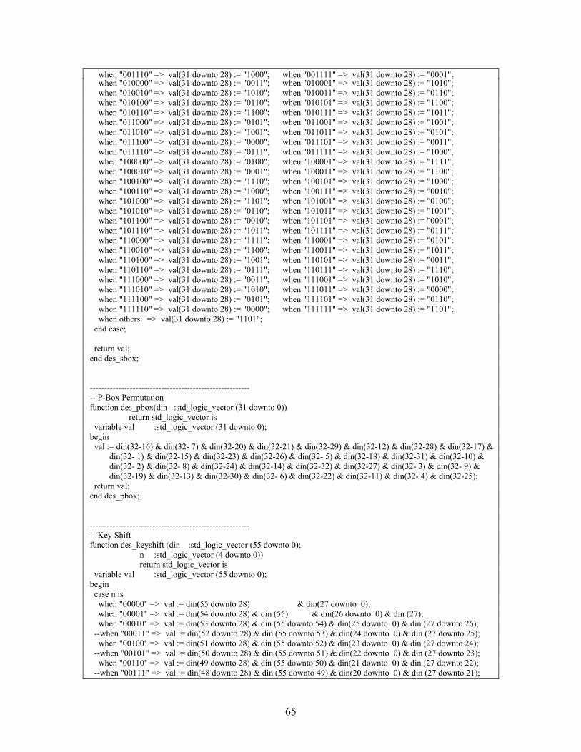
65
when "001110" => val(31 downto 28) := "1000"; when "001111" => val(31 downto 28) := "0001"; when "010000" => val(31 downto 28) := "0011"; when "010001" => val(31 downto 28) := "1010"; when "010010" => val(31 downto 28) := "1010"; when "010011" => val(31 downto 28) := "0110"; when "010100" => val(31 downto 28) := "0110"; when "010101" => val(31 downto 28) := "1100"; when "010110" => val(31 downto 28) := "1100"; when "010111" => val(31 downto 28) := "1011"; when "011000" => val(31 downto 28) := "0101"; when "011001" => val(31 downto 28) := "1001"; when "011010" => val(31 downto 28) := "1001"; when "011011" => val(31 downto 28) := "0101"; when "011100" => val(31 downto 28) := "0000"; when "011101" => val(31 downto 28) := "0011"; when "011110" => val(31 downto 28) := "0111"; when "011111" => val(31 downto 28) := "1000"; when "100000" => val(31 downto 28) := "0100"; when "100001" => val(31 downto 28) := "1111"; when "100010" => val(31 downto 28) := "0001"; when "100011" => val(31 downto 28) := "1100"; when "100100" => val(31 downto 28) := "1110"; when "100101" => val(31 downto 28) := "1000"; when "100110" => val(31 downto 28) := "1000"; when "100111" => val(31 downto 28) := "0010"; when "101000" => val(31 downto 28) := "1101"; when "101001" => val(31 downto 28) := "0100"; when "101010" => val(31 downto 28) := "0110"; when "101011" => val(31 downto 28) := "1001"; when "101100" => val(31 downto 28) := "0010"; when "101101" => val(31 downto 28) := "0001"; when "101110" => val(31 downto 28) := "1011"; when "101111" => val(31 downto 28) := "0111"; when "110000" => val(31 downto 28) := "1111"; when "110001" => val(31 downto 28) := "0101"; when "110010" => val(31 downto 28) := "1100"; when "110011" => val(31 downto 28) := "1011"; when "110100" => val(31 downto 28) := "1001"; when "110101" => val(31 downto 28) := "0011"; when "110110" => val(31 downto 28) := "0111"; when "110111" => val(31 downto 28) := "1110"; when "111000" => val(31 downto 28) := "0011"; when "111001" => val(31 downto 28) := "1010"; when "111010" => val(31 downto 28) := "1010"; when "111011" => val(31 downto 28) := "0000"; when "111100" => val(31 downto 28) := "0101"; when "111101" => val(31 downto 28) := "0110"; when "111110" => val(31 downto 28) := "0000"; when "111111" => val(31 downto 28) := "1101"; when others => val(31 downto 28) := "1101"; end case; return val; end des_sbox; -------------------------------------------------------- -- P-Box Permutation function des_pbox(din :std_logic_vector (31 downto 0)) return std_logic_vector is variable val :std_logic_vector (31 downto 0); begin val := din(32-16) & din(32- 7) & din(32-20) & din(32-21) & din(32-29) & din(32-12) & din(32-28) & din(32-17) & din(32- 1) & din(32-15) & din(32-23) & din(32-26) & din(32- 5) & din(32-18) & din(32-31) & din(32-10) & din(32- 2) & din(32- 8) & din(32-24) & din(32-14) & din(32-32) & din(32-27) & din(32- 3) & din(32- 9) & din(32-19) & din(32-13) & din(32-30) & din(32- 6) & din(32-22) & din(32-11) & din(32- 4) & din(32-25); return val; end des_pbox; -------------------------------------------------------- -- Key Shift function des_keyshift (din :std_logic_vector (55 downto 0); n :std_logic_vector (4 downto 0)) return std_logic_vector is variable val :std_logic_vector (55 downto 0); begin case n is when "00000" => val := din(55 downto 28) & din(27 downto 0); when "00001" => val := din(54 downto 28) & din (55) & din(26 downto 0) & din (27); when "00010" => val := din(53 downto 28) & din (55 downto 54) & din(25 downto 0) & din (27 downto 26); --when "00011" => val := din(52 downto 28) & din (55 downto 53) & din(24 downto 0) & din (27 downto 25); when "00100" => val := din(51 downto 28) & din (55 downto 52) & din(23 downto 0) & din (27 downto 24); --when "00101" => val := din(50 downto 28) & din (55 downto 51) & din(22 downto 0) & din (27 downto 23); when "00110" => val := din(49 downto 28) & din (55 downto 50) & din(21 downto 0) & din (27 downto 22); --when "00111" => val := din(48 downto 28) & din (55 downto 49) & din(20 downto 0) & din (27 downto 21);

66
when "01000" => val := din(47 downto 28) & din (55 downto 48) & din(19 downto 0) & din (27 downto 20); --when "01001" => val := din(46 downto 28) & din (55 downto 47) & din(18 downto 0) & din (27 downto 19); when "01010" => val := din(45 downto 28) & din (55 downto 46) & din(17 downto 0) & din (27 downto 18); --when "01011" => val := din(44 downto 28) & din (55 downto 45) & din(16 downto 0) & din (27 downto 17); when "01100" => val := din(43 downto 28) & din (55 downto 44) & din(15 downto 0) & din (27 downto 16); --when "01101" => val := din(42 downto 28) & din (55 downto 43) & din(14 downto 0) & din (27 downto 15); when "01110" => val := din(41 downto 28) & din (55 downto 42) & din(13 downto 0) & din (27 downto 14); when "01111" => val := din(40 downto 28) & din (55 downto 41) & din(12 downto 0) & din (27 downto 13); --when "10000" => val := din(39 downto 28) & din (55 downto 40) & din(11 downto 0) & din (27 downto 12); when "10001" => val := din(38 downto 28) & din (55 downto 39) & din(10 downto 0) & din (27 downto 11); --when "10010" => val := din(37 downto 28) & din (55 downto 38) & din( 9 downto 0) & din (27 downto 10); when "10011" => val := din(36 downto 28) & din (55 downto 37) & din( 8 downto 0) & din (27 downto 9); --when "10100" => val := din(35 downto 28) & din (55 downto 36) & din( 7 downto 0) & din (27 downto 8); when "10101" => val := din(34 downto 28) & din (55 downto 35) & din( 6 downto 0) & din (27 downto 7); --when "10110" => val := din(33 downto 28) & din (55 downto 34) & din( 5 downto 0) & din (27 downto 6); when "10111" => val := din(32 downto 28) & din (55 downto 33) & din( 4 downto 0) & din (27 downto 5); --when "11000" => val := din(31 downto 28) & din (55 downto 32) & din( 3 downto 0) & din (27 downto 4); when "11001" => val := din(30 downto 28) & din (55 downto 31) & din( 2 downto 0) & din (27 downto 3); --when "11010" => val := din(29 downto 28) & din (55 downto 30) & din( 1 downto 0) & din (27 downto 2); when "11011" => val := din(28 ) & din (55 downto 29) & din( 0 ) & din (27 downto 1); when others => val := din; end case; return val; end des_keyshift; end des_lib; ---------------------------------------------------------------------------- ---------------------------------------------------------------------------- library ieee; use ieee.std_logic_1164.all; use ieee.std_logic_arith.all; use ieee.std_logic_unsigned.all; library work; use work.des_lib.all; entity des_round is port (clk :in std_logic; reset :in std_logic; stall :in std_logic; encrypt_in :in std_logic; encrypt_shift :in std_logic_vector (4 downto 0); decrypt_shift :in std_logic_vector (4 downto 0); key_in :in std_logic_vector (55 downto 0); din :in std_logic_vector (63 downto 0); din_valid :in std_logic; encrypt_out :out std_logic; key_out :out std_logic_vector (55 downto 0); dout :out std_logic_vector (63 downto 0); dout_valid :out std_logic ); end des_round; architecture arch_des_round of des_round is begin process (clk, reset, stall, key_in, din, din_valid, encrypt_IN, encrypt_shift, decrypt_shift)

67
variable key :std_logic_vector (47 downto 0); variable data_ep :std_logic_vector (47 downto 0); variable data_sbox :std_logic_vector (31 downto 0); variable data_pbox :std_logic_vector (31 downto 0); begin if reset='1' then key_out <= "00000000000000000000000000000000000000000000000000000000"; dout <= "0000000000000000000000000000000000000000000000000000000000000000"; dout_valid <= '0'; encrypt_out <= '0'; elsif clk'event and clk='1' then if stall='0' then -- Handle the key encrypt_out <= encrypt_in; key_out <= key_in; if encrypt_in='1' then key := des_cp(des_keyshift(key_in,encrypt_shift)); else key := des_cp(des_keyshift(key_in,decrypt_shift)); end if; -- Handle the data data_ep := des_ep(din(31 downto 0)) xor key; data_sbox := des_sbox(data_ep); data_pbox := des_pbox(data_sbox) xor din(63 downto 32); dout <= din(31 downto 0) & data_pbox; dout_valid <= din_valid; end if; end if; end process; end arch_des_round; ---------------------------------------------------------------------------- ---------------------------------------------------------------------------- -- entity des_fast removed here ---------------------------------------------------------------------------- ---------------------------------------------------------------------------- library ieee; use ieee.std_logic_1164.all; use ieee.std_logic_arith.all; use ieee.std_logic_unsigned.all; library work; use work.des_lib.all; entity des_small is port (clk :in std_logic; reset :in std_logic; encrypt :in std_logic; key_in :in std_logic_vector (55 downto 0); din :in std_logic_vector (63 downto 0); din_valid :in std_logic; busy :out std_logic; dout :out std_logic_vector (63 downto 0); dout_valid :out std_logic ); end des_small;

68
architecture arch_des_small of des_small is type STATES is (IDLE, WORKING); signal state :STATES := IDLE; signal round :std_logic_vector (3 downto 0) := "0000"; signal stall :std_logic := '0'; signal key :std_logic_vector (55 downto 0) := "00000000000000000000000000000000000000000000000000000000"; signal encrypt_flag :std_logic := '1'; signal encrypt_in :std_logic := '1'; signal encrypt_shift :std_logic_vector (4 downto 0) := "00000"; signal decrypt_shift :std_logic_vector (4 downto 0) := "00000"; signal r_key_in :std_logic_vector (55 downto 0) := "00000000000000000000000000000000000000000000000000000000"; signal r_din :std_logic_vector (63 downto 0) := "0000000000000000000000000000000000000000000000000000000000000000"; signal r_dout :std_logic_vector (63 downto 0) := "0000000000000000000000000000000000000000000000000000000000000000"; signal dummy1 :std_logic := '0'; signal dummy2 :std_logic := '0'; signal dummy3 :std_logic := '0'; signal dummy4 :std_logic_vector (55 downto 0) := "00000000000000000000000000000000000000000000000000000000"; begin -- Manage the IDLE/WORKING state machine process (clk, reset, round, din_valid) begin if reset='1' then state <= IDLE; elsif clk'event and clk='1' then case state is when IDLE => if din_valid='1' then state <= WORKING; end if; when WORKING => if (round="1111") then state <= IDLE; end if; end case; end if; end process; -- Track the current DES round process (clk, reset, din_valid, state) begin if reset='1' then round <= "0000"; elsif clk'event and clk='1' then if state/=IDLE then round <= round + 1; elsif din_valid='1' then round <= round + 1; else round <= "0000"; end if;

69
end if; end process; -- Generate the busy signal process (clk, reset, state, round, din_valid) begin if reset='1' then busy <= '0'; elsif clk'event and clk='1' then if state=IDLE and din_valid='0' then busy <= '0'; elsif round="1111" then busy <= '0'; else busy <= '1'; end if; end if; end process; -- Latch the encrypt_flag, key process (clk, reset, state, din_valid, encrypt, key_in) begin if reset='1' then encrypt_flag <= '0'; key <= "00000000000000000000000000000000000000000000000000000000"; elsif clk'event and clk='1' then if state=IDLE and din_valid='1' then encrypt_flag <= encrypt; key <= key_in; end if; end if; end process; -- Mux the inputs to des_round encrypt_in <= encrypt when state=IDLE else encrypt_flag; r_key_in <= key_in when state=IDLE else key; r_din <= des_ip(din) when state=IDLE else r_dout; dummy1 <= '0'; stall <= '0'; -- Do the round ROUND0: des_round port map (clk, reset, stall, encrypt_in, encrypt_shift, decrypt_shift, r_key_in, r_din, dummy1, dummy2, dummy4, r_dout, dummy3); -- Generate the encrypt/decrypt key shift amounts: process (round) begin case round is when "0000" => encrypt_shift <= "00001"; decrypt_shift <= "00000"; when "0001" => encrypt_shift <= "00010"; decrypt_shift <= "11011"; when "0010" => encrypt_shift <= "00100"; decrypt_shift <= "11001"; when "0011" => encrypt_shift <= "00110"; decrypt_shift <= "10111"; when "0100" => encrypt_shift <= "01000"; decrypt_shift <= "10101"; when "0101" => encrypt_shift <= "01010"; decrypt_shift <= "10011"; when "0110" => encrypt_shift <= "01100"; decrypt_shift <= "10001"; when "0111" => encrypt_shift <= "01110"; decrypt_shift <= "01111"; when "1000" => encrypt_shift <= "01111"; decrypt_shift <= "01110"; when "1001" => encrypt_shift <= "10001"; decrypt_shift <= "01100";

70
when "1010" => encrypt_shift <= "10011"; decrypt_shift <= "01010"; when "1011" => encrypt_shift <= "10101"; decrypt_shift <= "01000"; when "1100" => encrypt_shift <= "10111"; decrypt_shift <= "00110"; when "1101" => encrypt_shift <= "11001"; decrypt_shift <= "00100"; when "1110" => encrypt_shift <= "11011"; decrypt_shift <= "00010"; when "1111" => encrypt_shift <= "00000"; decrypt_shift <= "00001"; when others => encrypt_shift <= "00001"; decrypt_shift <= "00000"; end case; end process; -- Generate the dout_valid signal process (clk, reset, round) begin if reset='1' then dout_valid <= '0'; elsif clk'event and clk='1' then if round="1111" then dout_valid <= '1'; else dout_valid <= '0'; end if; end if; end process; -- Output the data dout <= des_fp(r_dout(31 downto 0) & r_dout(63 downto 32)); end arch_des_small; ---------------------------------------------------------------------------- ---------------------------------------------------------------------------- ---------------------------------------------------------------------------- ----------------------------------------------------------------------------
Figure A.2 freedes.vhd, VHDL DES Core ---------------------------------------------------------------------------- ---------------------------------------------------------------------------- -- The Free IP Project -- VHDL DES Core -- (c) 1999, The Free IP Project and David Kessner -- -- -- Warning: This software probably falls under the jurisdiction of some -- cryptography import/export laws. Don't import/export this -- file (or products that use this file) unless you've worked -- out all the legal issues. Don't say we didn't warn you! -- -- -- FREE IP GENERAL PUBLIC LICENSE -- TERMS AND CONDITIONS FOR USE, COPYING, DISTRIBUTION, AND MODIFICATION -- -- 1. You may copy and distribute verbatim copies of this core, as long -- as this file, and the other associated files, remain intact and -- unmodified. Modifications are outlined below. Also, see the -- import/export warning above for further restrictions on -- distribution. -- 2. You may use this core in any way, be it academic, commercial, or -- military. Modified or not. See, again, the import/export warning

71
-- above. -- 3. Distribution of this core must be free of charge. Charging is -- allowed only for value added services. Value added services -- would include copying fees, modifications, customizations, and -- inclusion in other products. -- 4. If a modified source code is distributed, the original unmodified -- source code must also be included (or a link to the Free IP web -- site). In the modified source code there must be clear -- identification of the modified version. -- 5. Visit the Free IP web site for additional information. -- ---------------------------------------------------------------------------- ---------------------------------------------------------------------------- library ieee; use ieee.std_logic_1164.all; use ieee.std_logic_arith.all; use ieee.std_logic_unsigned.all; package destest_lib is --component des_fast_testbench --end component; component des_small_testbench end component; -- function random32 removed function random56 (din:std_logic_vector(55 downto 0)) return std_logic_vector; function random64 (din:std_logic_vector(63 downto 0)) return std_logic_vector; end destest_lib; ---------------------------------------------------------------------------- ---------------------------------------------------------------------------- library ieee; use ieee.std_logic_1164.all; use ieee.std_logic_arith.all; use ieee.std_logic_unsigned.all; library work; use work.destest_lib.all; package body destest_lib is -- function random 32 removed function random56 (din:std_logic_vector(55 downto 0)) return std_logic_vector is variable val :std_logic_vector (55 downto 0); begin val := (din(55) xor din(6) xor din(3) xor din(1)) & din(55 downto 1); return (val); end random56; function random64 (din:std_logic_vector(63 downto 0)) return std_logic_vector is variable val :std_logic_vector (63 downto 0); begin val := (din(63) xor din(3) xor din(2) xor din(0)) & din(63 downto 1); return (val); end random64;

72
end destest_lib; ---------------------------------------------------------------------------- ---------------------------------------------------------------------------- -- removed entity des_fast_testbench ---------------------------------------------------------------------------- ---------------------------------------------------------------------------- library ieee; use ieee.std_logic_1164.all; use ieee.std_logic_arith.all; use ieee.std_logic_unsigned.all; library work; --use work.des_lib.all; use work.destest_lib.all; entity des_small_testbench is -- port(); end des_small_testbench; architecture tb_des of des_small_testbench is signal clk :std_logic := '1'; signal reset :std_logic := '1'; signal key :std_logic_vector (55 downto 0) := "00000000000000000000000000000000000000000000000000000000"; signal din :std_logic_vector (63 downto 0) := "0000000000000000000000000000000000000000000000000000000000000000"; signal din_valid :std_logic := '0'; signal dout1 :std_logic_vector (63 downto 0) := "0000000000000000000000000000000000000000000000000000000000000000"; signal dout2 :std_logic_vector (63 downto 0) := "0000000000000000000000000000000000000000000000000000000000000000"; signal dout_valid1 :std_logic := '0'; signal dout_valid2 :std_logic := '0'; signal encrypt_flag :std_logic := '1'; signal decrypt_flag :std_logic := '0'; signal busy1 :std_logic := '1'; signal busy2 :std_logic := '1'; component des_small ---------------------- new for textIO --------------------- generic (print: boolean); ---------------------- end new ---------------------------- port ( clk : in STD_LOGIC := 'X'; reset : in STD_LOGIC := 'X'; encrypt : in STD_LOGIC := 'X'; key_in : in STD_LOGIC_VECTOR ( 55 downto 0 ); din : in STD_LOGIC_VECTOR ( 63 downto 0 ); din_valid : in STD_LOGIC := 'X'; busy : out STD_LOGIC; dout : out STD_LOGIC_VECTOR ( 63 downto 0 ); dout_valid : inout STD_LOGIC ); end component; begin

73
process (clk) begin if clk='1' then clk <= '0' after 25 ns, '1' after 50 ns; end if; end process; reset <= '1' after 0 ns, '0' after 25 ns; -- Generate the random key's and random data process (reset, clk) --, busy1, busy2) begin if reset='1' then din_valid <= '0'; din <= "0010100100110110001001011011001111001011001001100010010100011001"; key <= "10100101010010010100101010001101010001011001111110000111"; elsif clk'event and clk='1' then --if dout_valid2='1' then if din_valid='0' and busy1='0' and busy2='0' and dout_valid1='0' and dout_valid2='0' then din_valid <= '1' after 10 ns; --din <= "0000000000000000000000000000000000000000000000000000000000000000" after 35 ns; --key <= "00110000100001000100011001001110110000110100111101000011" after 35 ns; din <= random64(din); key <= random56(key); else din_valid <= '0' after 10 ns; end if; end if; end process; -- Do the DES encryption/decryption blocks encrypt_flag <= '1'; decrypt_flag <= '0'; DES0: des_small --------------- new for textIO ------------------- generic map (true) ---------------- end new ------------------------- port map (clk, reset, encrypt_flag, key, din, din_valid, busy1, dout1, dout_valid1); DES1: des_small ----------------- new for textIO ------------------ generic map (false) ----------------- end new ------------------------- port map (clk, reset, decrypt_flag, key, dout1, dout_valid1, busy2, dout2, dout_valid2); -- Verify the unencrypted output process (clk, din, dout_valid2) variable check :std_logic_vector (63 downto 0); begin if clk'event and clk='1' then if dout_valid2='1' then if din/=dout2 then assert 1=0 report "Simulation Ended, DES Small Failed!!!!!!!!!!!!!!!!!!!!!!!!!" severity failure; end if; end if; end if; end process;

74
end tb_des;
Firgure A.3 tb_des.vhd, Test Bench for VHDL DES Core ////////////////////////////////////////////////////////////////// // Larry McDaniel // 11/14/02 // // This program reads from a synthesized VHDL file searching // for lines that are held in a second file and then using the // found lines it create a new VHDL file that will count the // transistions of certain CLB outputs of the synthesized device // // Version 2 1/15/03 // This version includes additions including VHDL TEXTIO to print // output to a text file ////////////////////////////////////////////////////////////////// #include <fstream.h> #include <stdlib.h> #include <iostream> int main () { char vhdl_buff[100], comp_buff[100], node_buff[100]; int count = 0, z = 0; int answer, answer2, answer3; int i = 5, j = 0, match = 0, k = 0, l = 0, m = 0, match2 = 0; int begin_cnt = 0, end_cnt = 0, begin_look = 0, numcnt = 0; char hold[1500][100], hold2[1500][100]; ifstream infile ("time_sim.vhd"); ifstream infile3 ("nodes.txt"); ifstream infile4 ("ports.txt"); char * string1, * string2; int space_fnd = 0, go_cnt = 0, first_end = 0, done = 0, ent_fnd = 0; if (! infile.is_open()) { cout << "Error opening file"; exit (1); } ofstream SaveFile("testfile.vhd"); ofstream savesignal("signalnames.dat"); //for printing out new signal names // Run through VHDL file to find the important outputs by // comparing lines to component file while (! infile.eof() ) { infile.eatwhite(); // clears the white space in the line proceding real chars infile.getline(vhdl_buff, 99); //reads line from time_sim.vhd ifstream infile3 ("nodes.txt"); ifstream infile4 ("ports.txt"); while (! infile3.eof() ) { infile3.eatwhite(); infile3.getline(comp_buff, 99); //reads line of text.txt string1 = strstr(vhdl_buff, comp_buff); string2 = strstr(vhdl_buff, "PWR"); if (string1 != NULL && string2 == NULL && count < 1500) { match = 1; cout << " WE SHOULD HAVE ONE -->>> " << vhdl_buff << " & " << comp_buff << endl;

75
} answer = strncmp(vhdl_buff, "O => ", 4); if (answer == 0 && match == 1) { cout << "Found an output: " << vhdl_buff << endl; i = 5; j = 0; space_fnd = 0; while (i < 30 && space_fnd == 0) { if (vhdl_buff[i] == ' ') space_fnd = 1; else hold[count][j] = vhdl_buff[i]; i ++; j ++; } // end while (i != 30 || space_fnd == 0) cout << "Important signal: " << hold[count] << endl; count = count + 1; match = 0; } // end if } // end of while for component file infile3.close(); while (! infile4.eof() ) { infile4.eatwhite(); infile4.getline(node_buff, 99); //reads line of text.txt string1 = strstr(vhdl_buff, node_buff); if (string1 != NULL) { cout << vhdl_buff << endl; i = 0; j = 0; numcnt = 0; space_fnd = 0; while (i < 30 && space_fnd == 0) { if (vhdl_buff[i] == ' ') space_fnd = 1; else hold2[numcnt][j] = vhdl_buff[i]; i ++; j ++; } // while (i != 30 || space_fnd == 0) hold2[numcnt][j-1] = '\0'; cout << "Found this port: " << hold2[numcnt] << endl; cout << "vhdl_buff: " << vhdl_buff << endl; numcnt++; match2 = 0; } } } // end of while for vhdl file infile.close(); // Now run through the VHDL file a second time and insert signal declarations // and process ifstream infile5 ("time_sim.vhd"); while (! infile5.eof()) { infile5.eatwhite();

76
infile5.getline(vhdl_buff, 99); // Change to proper top level entity answer = strncmp(vhdl_buff, "entity des_small", 13); answer2 = strncmp(vhdl_buff, "begin", 5); answer3 = strncmp(vhdl_buff, "end Structure;", 12); // Finding the proper top level entity if (answer == 0 && begin_look == 0) { begin_look = 1; cout << "Guess it found the entity statement" << endl; ////////////////////new for cnt outputs ///////////////////// SaveFile << "use STD.TEXTIO.all;" << endl; ent_fnd = 1; //////////////////////////////////////////////////////////// } else if (answer2 == 0 && begin_cnt == 0 && begin_look == 1) { cout << "Found the begin statement" << endl; begin_cnt = 1; cout << "########## Signal declarations &&&&&&&&&&" << endl; SaveFile << "signal "; j = 0; while (j < count) { k = 0; while (k < 10) { if (hold[j][k] == '(' || hold[j][k] ==')') hold[j][k] = '_'; else hold[j][k] = hold[j][k]; k++; } z = 0; while (z < 56) { SaveFile << "ATRAN_" << hold[j] << "_" << z << "bit0cnt, "; SaveFile << "ATRAN_" << hold[j] << "_" << z << "bit1cnt, "; // next two lines for printing out signal names savesignal << "ATRAN_" << hold[j] << "_" << z << "bit0cnt" << endl; savesignal << "ATRAN_" << hold[j] << "_" << z << "bit1cnt" << endl; z++; } SaveFile << "ATRAN_" << hold[j] << "_total_cnt"; // next line for printing out signal names savesignal << "ATRAN_" << hold[j] << "_total_cnt" << endl; if (j < count - 1) SaveFile << ", "; j++; } SaveFile << " : integer := 0;" << endl; } // else if else if (answer3 == 0 && count > 0) { cout << "trying to create the process" << endl; SaveFile << "TRANCOUNT:process (";

77
j = 0; while (j < count) { SaveFile << hold[j]; if (j < count - 1) SaveFile << ", "; j++; } SaveFile << ")" << endl; ///////////////// New for cnt outputs ///////////////////// SaveFile << "file out_file: text;" << endl; SaveFile << "variable OUTLINE: LINE;" << endl; /////////////////////////////////////////////////////////// SaveFile<< "begin" << endl; i = 0; while (i < numcnt) { j = 0; while (j < count) { k = 0; while (k < 10) { if (hold[j][k] == '(' || hold[j][k] ==')') hold[j][k] = '_'; else hold[j][k] = hold[j][k]; k++; } z = 0; while (z < 56) { SaveFile << "if (" << hold[j] << "'event and " << hold2[i] << "(" << z << ") = '0') then" << endl << "ATRAN_" << hold[j] << "_" << z << "bit0cnt <= ATRAN_" << hold[j] << "_" << z << "bit0cnt + 1;" << endl << "end if;" << endl; SaveFile << "if (" << hold[j] << "'event and " << hold2[i] << "(" << z << ") = '1') then" << endl << "ATRAN_" << hold[j] << "_" << z << "bit1cnt <= ATRAN_" << hold[j] << "_" << z << "bit1cnt + 1;" << endl << "end if;" << endl; z++; } SaveFile << "if (" << hold[j] << "'event) then" << endl << "ATRAN_" << hold[j] << "_total_cnt" << " <= " << "ATRAN_" << hold[j] << "_total_cnt + 1;" << endl << "end if;" << endl; j++; } i++; } // end while (i < numcnt) ////////// New for cnt outputs ////////////////////// SaveFile << "if (print) then" << endl; SaveFile << "file_open(out_file, \"cnt_output.txt\", write_mode);" << endl; SaveFile << "write(OUTLINE, \"Current Outputs\");" << endl; SaveFile << "writeline(out_file, OUTLINE);" << endl; j = 0; while (j < count)

78
{ z = 0; while (z < 56) { SaveFile << "write (OUTLINE, ATRAN_" << hold[j] << "_" << z << "bit0cnt);" << endl; SaveFile << "writeline (out_file, OUTLINE);" << endl; SaveFile << "write (OUTLINE, ATRAN_" << hold[j] << "_" << z << "bit1cnt);" << endl; SaveFile << "writeline (out_file, OUTLINE);" << endl; z++; } SaveFile << "write (OUTLINE, ATRAN_" << hold[j] << "_total_cnt);" << endl; SaveFile << "writeline (out_file, OUTLINE);" << endl; j++; } SaveFile << "file_close(out_file);" << endl; SaveFile << "end if;" << endl; SaveFile << "end process TRANCOUNT;" << endl; end_cnt = 1; } SaveFile << vhdl_buff; SaveFile << "\n"; //////////////////////////////new for cnts ///////////////////////////// if (ent_fnd == 1) { SaveFile << "generic(print: boolean);" << endl; ent_fnd = 0; } /////////////////////////////////////////////////////////////////////// }// end while cout << "Count is " << count << endl; return 0; SaveFile.close(); infile5.close(); } // end of main
Figure A.4 C++ Code to Alter the Synthesized VHDL Code % ----------------------------------------------------------------------------% % Larry McDaniel % % Matlab code to operate on results of instrmented VHDL file %-----------------------------------------------------------------------------% fid = fopen('matlab_samples.txt'); % open results file while feof(fid) == 0 a = fscanf(fid, '%d', 100457); % read in results one encryption at a time asize = size(a); if asize(1) > 0 i = 1; while i <= asize(1) if a(i) > 1 m(i) = m(i) + a(i); % sum transition count for each signal
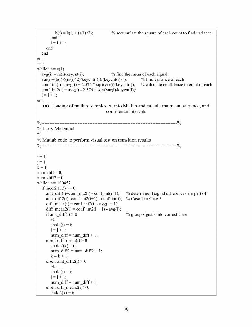
79
b(i) = b(i) + (a(i)^2); % accumulate the square of each count to find variance end i = i + 1; end end end i=1; while i <= s(1) avg(i) = m(i)/keycnt(i); % find the mean of each signal var(i)=(b(i)-((m(i)^2)/keycnt(i)))/(keycnt(i)-1); % find variance of each conf_int(i) = avg(i) + 2.576 * sqrt(var(i)/keycnt(i)); % calculate confidence internal of each conf_int2(i) = avg(i) - 2.576 * sqrt(var(i)/keycnt(i)); i = i + 1; end
(a) Loading of matlab_samples.txt into Matlab and calculating mean, variance, and confidence intervals
%----------------------------------------------------------------------------------% % Larry McDaniel % % Matlab code to perform visual test on transition results %----------------------------------------------------------------------------------% i = 1; j = 1; k = 1; num_diff = 0; num_diff2 = 0; while i <= 100457 if mod(i,113) ~= 0 amt_diff(i)=conf_int2(i) - conf_int(i+1); % determine if signal differences are part of amt_diff2(i)=conf_int2(i+1) - conf_int(i); % Case 1 or Case 3 diff_mean(i) = conf_int2(i) - avg(i + 1); diff_mean2(i) = conf_int2(i + 1) - avg(i); if amt_diff(i) > 0 % group signals into correct Case %i shold(j) = i; j = j + 1; num_diff = num_diff + 1; elseif diff_mean(i) > 0 shold2(k) = i; num_diff2 = num_diff2 + 1; k = k + 1; elseif amt_diff2(i) > 0 %i shold(j) = i; j = j + 1; num_diff = num_diff + 1; elseif diff_mean2(i) > 0 shold2(k) = i;
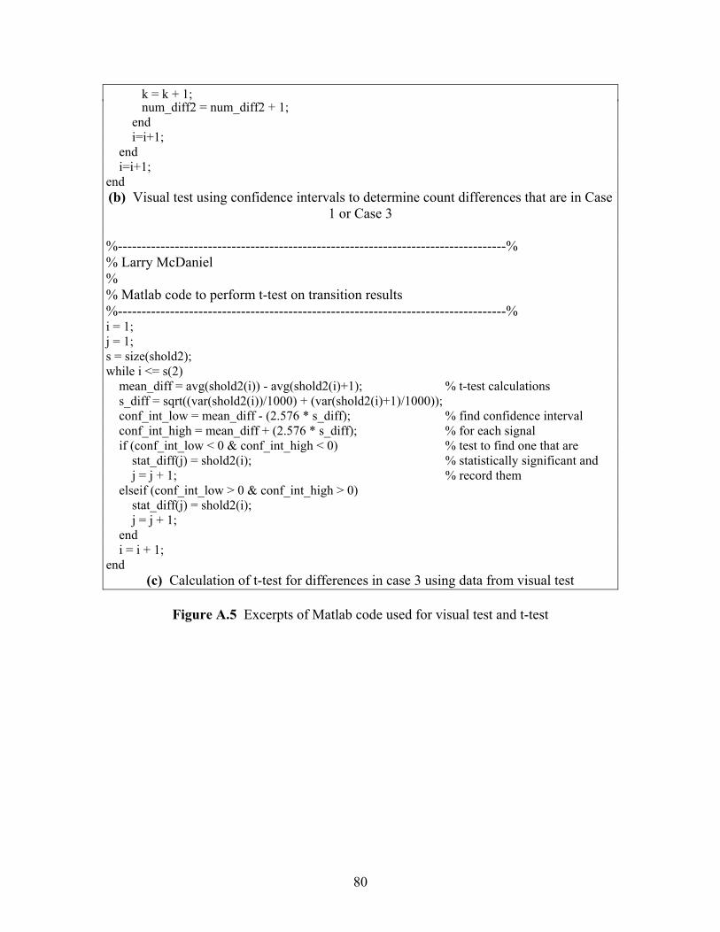
80
k = k + 1; num_diff2 = num_diff2 + 1; end i=i+1; end i=i+1; end (b) Visual test using confidence intervals to determine count differences that are in Case
1 or Case 3 %----------------------------------------------------------------------------------% % Larry McDaniel % % Matlab code to perform t-test on transition results %----------------------------------------------------------------------------------% i = 1; j = 1; s = size(shold2); while i <= s(2) mean_diff = avg(shold2(i)) - avg(shold2(i)+1); % t-test calculations s_diff = sqrt((var(shold2(i))/1000) + (var(shold2(i)+1)/1000)); conf_int_low = mean_diff - (2.576 * s_diff); % find confidence interval conf_int_high = mean_diff + (2.576 * s_diff); % for each signal if (conf_int_low < 0 & conf_int_high < 0) % test to find one that are stat_diff(j) = shold2(i); % statistically significant and j = j + 1; % record them elseif (conf_int_low > 0 & conf_int_high > 0) stat_diff(j) = shold2(i); j = j + 1; end i = i + 1; end
(c) Calculation of t-test for differences in case 3 using data from visual test
Figure A.5 Excerpts of Matlab code used for visual test and t-test

81
Vita Larry Thomas McDaniel III was born on January 31, 1979 in Danville, VA. In May
2001, he received his Bachelors of Science degree in Electrical Engineering from
Virginia Commonwealth University in Richmond, VA. Larry received his Masters of
Science degree in Electrical Engineering in May 2003 from Virginia Polytechnic Institute
and State University in Blacksburg, VA. He will join the Signal Exploitation and
Geolocation division of Southwest Research Institute, in San Antonio, Texas, as a
Research Engineer in July 2003.