laser assisted machining proce ss of hiped silicon nitride assisted machining proce ss of hiped...
TRANSCRIPT
JLMN-Journal of Laser Micro/Nanoengineering Vol. 4, No. 3, 2009
207
Laser Assisted Machining Process of HIPed Silicon Nitride Jaehoon LEE*1, Sehwan LIM*1, Dongsig SHIN*1, Hyonkee SOHN*1, Jongdo KIM*2, Joohyun KIM*3
*1 Korea Institute of Machinery & Materials, Sinseongno 104, Yuseong-gu, DaeJeon, Korea E-mail: [email protected]
*2 Korea Maritime University, Dongsam-dong 1, Youngdo-gu, Busan, Korea *3 Kookmin University, Jeongneung-gil 77, Jeongneung-dong, Seongbuk-gu, Seoul, Korea
In this study, fiber coupled HPDL was employed for Laser-Assisted Machining (LAM) of Hot Isostatically Pressed (HIPed) silicon nitride workpieces. In LAM, the intense energy of laser was used to enhance the machinability by locally heating the workpiece and thus reducing its yield strength. In this experiment, the laser power ranged from 200 W to 800 W while the diameter of the workpiece was 16mm. While machining, the surface temperature was kept nearly constant by laser heating after a preheat phase of 58 seconds. Microscopy observations of machined surfaces and chips were performed to understand the mechnical behavior of silicon nitride with temperature. The effects of chip formation temperature on machining characteristics were assessed by measuring the cutting forces and flank wear. At a temperature of about 1153℃, a good quality machined surface on the HIPed silicon nitride workpiece was obtained with no grain pullout regions and little oxida-tion layer.
Keywords: Laser-assisted machining(LAM), Silicon nitride(Si3N4), Hot isostatic pressing(HIP), Machined surface, Chip, Cutting force, Flank wear
1. Introduction
Due to their hardness and brittle nature, engineering ce-ramics are typically machined by grinding and diamond machining. These processes represent 60 to 90 percent of the cost of the final product owing to the low Material Re-moval Rate (MRR) and the high wear rate of the cutting medium [1]. Alternatively, Laser Assisted Machining (LAM) may yield substantial cost savings due to higher material removal rates, reduced man and machine hours per part, and the increased tool life.
In LAM, the intense energy of laser beam was used to enhance the machinability by locally heating the workpiece in order to change the deformation behavior of the material from brittle to ductile.
Silicon nitride is one of the most promising structural ceramics because of its low density, as well as high wear resistance and oxidation resistance compared with other ceramic materials. Moreover, silicon nitride is suitable for LAM because of low thermal expansion, high thermal con-duction, and fracture toughness [2-9].
Rozzi, J.C. et al. [2-4] developed a three-dimensional heat transfer model for predicting the temperature distribu-tions of chip formation zone. They also performed the LAM test in order to evaluate the effects of LAM parame-ters on the machining characteristics. Lei, S. et al. [5-6] investigated the material removal mechanisms associated with LAM by observing the resulting chips and formulated a constitutive model for predicting the effects of operating conditions on the shear zone stress. Tian, Y. et al. [7-9] developed a three-dimensional thermal model to predict the temperature distribution in a silicon nitride workpiece that had complex features undergoing LAM. This model was applied to LAM on silicon nitride parts that had complex
features to ensure the optimal material removal temperature. They also studied the discontinuous chip formation mecha-nism by using multiscale FEM.
These investigations have shown that LAM can achieve lower cutting forces, reduced tool wear, higher material removal rates, and better surface quality. However, the used workpieces were limited to a sintered silicon nitride with a diameter of less than 8.5 mm.
This study evaluated LAM for Hot Isostatically Pressed (HIPed) silicon nitride. Due to its little residual flaws and porosity, HIPed silicon nitride workpieces were more diffi-cult to be machined compared to the pressureless sintered silicon nitride workpieces [10]. Nevertheless, HIP has a main advantage for silicon nitride in that its possibility in being nearly net-shaped eliminates post machining of the densified part, except for surfaces with extremely close tolerances.
In this study, surface temperature histories were meas-ured by a pyrometer, which kept a relative position to the laser spot during preheat and translation phase. The mate-rial deformation behavior was studied by observing the machined surfaces and chips. The machining characteris-tics that had temperature variation were investigated by measuring the cutting forces and flank wear.
2. Experimental method
Fig. 1 shows the laser-integrated machine that was em-ployed for the LAM experiment. The machine consisted of an optic module integrated into a turret lathe. By combin-ing both conventional metal cutting technologies with laser processes in one machine, the complete processing of a workpiece by using different technologies in one setting can be realized.

JLMN-Journal of Laser Micro/Nanoengineering Vol. 4, No. 3, 2009
208
For the LAM experiment, the cutting tool and the py-rometer were located at (Фlt = 180°, Llt = 2.3 mm) and (Фlt = 90°, Llt = 0 mm), respectively.
The turning operation took place on an AML200TLSY (26 kW) CNC turret lathe equipped with a 31iTB controller (FANUC). An assist gas (air) was supplied to the laser nozzle in order to protect the optics from any debris gener-ated during LAM. TaeguTec CNMA120408 LN TB650 polycrystalline cubic boron nitride (PCBN) tipped carbide insert (negative rake angle, -5°) was clamped on the PCLNR-2525 tool holder during the LAM of silicon nitride. Three cutting force components, such as the cutting force (Fc), the thrust force (Ft), and the feed force (Ff) were re-corded by a dynamometer (KISTLER, 9257B type) at a frequency of 5 Hz.
A High Power Diode Laser (HPDL) was used because of the possibility of the beam being delivered by optical fiber, as well as having high efficiency and a low cost for setup and maintenance. Continuous wave HPDL system (LASERLINE, LDF1000-2500) with a maximum rated power of 2.5 kW had coupled wavelengths of 910 nm and 980 nm. 5 mm × 5 mm (50 % of the peak) square shape laser beam, which was used for the LAM of silicon nitride, was prepared by a homogenizer and a focusing lens at the working distance of 158 mm, as shown in Fig. 2.
Fig. 1 Experimental system for laser-assisted machining of silicon nitride
Fig. 2 Laser beam profile for laser-assisted machining of silicon nitride
The flat top shaped beam is advantageous for uniform heating of silicon nitride while a Gaussian beam may lead to ablation of the material due to the unequal beam prop-erty.
Surface temperature measurements are crucial for un-derstanding phenomena that depend on the LAM process parameters. In this study, the off-axis pyrometer (KLEIBER, KGAF730) operated over a single waveband and had the ability to measure temperature in a range of 300–2300℃.
The cylindrical silicon nitride workpiece, which has a diameter of 16 mm and a length of 150 mm, was hot-isostatic pressed with alumina (Al2O3) and yttria(Y2O3), resulting in 90 wt% β-Si3N4 grains and 10 wt% YSiAlON glass.
The LAM experiment consisted of two phases: 1) a preheat phase in which the laser beam irradiated at the end of the rotating workpiece (l = 2 mm in Fig. 1) without any axial translation of the laser and the cutting tool and 2) a material removal phase in which the laser and cutting tool moved axially along the workpiece. The preheat phase al-lowed for an acceptable chip formation temperature before material removal was initiated. A preheating time of 58 sec for was needed for a silicon nitride workpiece that had a diameter of 16 mm. The material properties of the HIPed silicon nitride workpiece are listed in Table 1.
The laser power was controlled in a range that ranged from 200 W to 800 W in order to assess the effect of chip formation temperature on machining characteristics. Other parameters, such as the rotational speed of 620 rpm (cutting speed of 31.16 m/min), depth of cut of 0.3 mm, and the feed rate of 0.013 mm/rev were also fixed.
3. Heating test
After preheating for 58 sec, laser beam traveled 70mm in the axial direction without any material removal. The relative position of the pyrometer (фlp=90°, Llp=0mm) with the laser beam was maintained for monitoring surface tem-poral temperature.
The measured surface temperatures, Tmea, with various laser powers are shown in Table 2 and Fig. 3. During the preheat phase, the surface temperatures approached a quasi-saturation temperature for each laser power and were kept constant during laser/pyrometer translation.
Table 1 Thermal and mechanical properties of the HIPed silicon nitride
Vickers hardness (GPa) 14 Flexural strength (MPa) 610-880
Compressive strength (MPa) 3820
Young’s modulus (GPa) 290-300
Poisson’s ratio 0.28
Fracture toughness (MPa ) 5-6 Coefficient of linear thermal expansion (10-6℃-1) 2.6-3.2
Thermal conductivity (W/mK) 20-30
Specific heat (J/kgK) 660
Density (kg/m3) 3200

JLMN-Journal of Laser Micro/Nanoengineering Vol. 4, No. 3, 2009
209
Fig. 3 Surface temperature histories during the heating tests
with laser power and feed rate (фlp=90°)
It was predicted that the surface temperature at the measurement location (фlp = 90°, Llp = 0 mm), Tmea would be 10 % lower than the maximum surface temperature, Tmax , and 10 % higher than the surface temperature at the chip formation zone, Tch , as the preliminary tests showed in Table 2.
Fig. 4 shows the surface of the heating test workpiece. When the maximum surface temperature increased to 1414℃, noticeable oxidation started to occur, as shown in Figure 4(b). At temperatures higher than 1633℃, porous structure on the surface was formed, as shown in Fig. 4(c).
Tian, Y. et al. [8] studied the oxidation and the porous structure of silicon nitride in LAM. They showed that the oxidation resulted in Y2Si2O7 and SiO2 on the surface in the temperature range of 1420℃<Tmax<1620℃. At tempera-tures higher than approximately 1680℃, the glass phase start to melt and severe oxidation produced nitrogen gas bubbles, and the burst of the bubbles consequently formed the porous structure.
The SEM micrographs in Fig. 5 revealed the cross sec-tions of the heating test workpieces. Despite the severe oxidation and melting at the surface temperature above 1633℃, no thermal damage of the subsurface occurred because the oxidation layer served as a protective film and retarded further oxidation beneath the surface.
4. Machining test
Fig. 6 is schematic sketch for the semi-continuous chip formation of silicon nitride material undergoing LAM. Chip formation occurred by visco-plastic flow of YSiAlON glassy grain-boundary phase at a temperature above the YSiAlON glass transition temperature (920~970�). The rod-like Si3N4 grains at the shear deformation zone begin to slip at the grain boundaries, while they rotated and experi-
enced mutual interactions along the flow of the YSiAlON glassy phase.
(a) (b)
(c) (d)
Fig. 4 Photographs of heated surfaces with various maxi-
mum surface temperature: (a) 977℃, (b)1414℃, (c) 1633℃ and (d) 1795℃
(a) (b)
(c) (d)
Fig. 5 SEM micrographs of cross sections with various
maximum surface temperature: (a) 977℃, (b)1414℃, (c) 1633℃ and (d) 1795℃
Fig. 6 Semi-continuous chip formation with intergranular fracture in LAM of silicon nitride
Table 2 Heating test conditions and measured sur-face temperatures (фlp = 90°)
No. Pl (W) Tmax (℃) Tmea (℃) Tch (℃) 1 200 977 888 796
2 400 1414 1286 1153
3 600 1633 1485 1332
4 800 1795 1632 1463

JLMN-Journal of Laser Micro/Nanoengineering Vol. 4, No. 3, 2009
210
Nucleation and propagation of intergranular micro-cracks resulted in segmented chip formation. During the LAM process, the Si3N4 grains behave as rigid bodies. LAM tests were performed in order to evaluate the machin-ing characteristics with chip formation temperatures. Fig. 7 and Fig. 8 are pictures of machined surfaces magnified by optical microscopy and SEM, respectively.
At the chip formation temperature of 796℃, Si3N4 grain pullout regions were observed because the severe intergranular cracks were propagated beneath a machined surface by the increased viscosity of the YSiAlON glassy phase. At a temperature of 1153℃, good quality of the machined surface was obtained with no grain pullout re-gions and little oxidation layer, but the oxidation layer worsened the machined surface quality as the temperature exceeded 1332℃.
(a) (b)
(c) (d)
Fig. 7 Optical micrographs of machined surface with vari-
ous chip formation temperature: (a) 796℃, (b)1153℃, (c) 1332℃ and (d) 1463℃
(a) (b)
(c) (d)
Fig. 8 SEM micrographs of machined surface with various
chip formation temperature: (a) 796℃, (b)1153℃, (c) 1332℃ and (d) 1463℃
Fig. 9 shows optical micrographs of chips with various chip formation temperatures. At the chip formation tem-perature of 796℃, intergranular fracture resulted in a dis-continuous chip formation. With increasing temperature, the chips generated during LAM became more congruent and semi-continuous. This phenomenon can be clearly ob-served by the SEM micrographs shown in Fig. 10. At a temperature of 796℃, Si3N4 grains at the chip were ex-posed owing to the intergranular fracture. The fluidity of intergranular glassy phase increased when the chip forma-tion temperature increased.
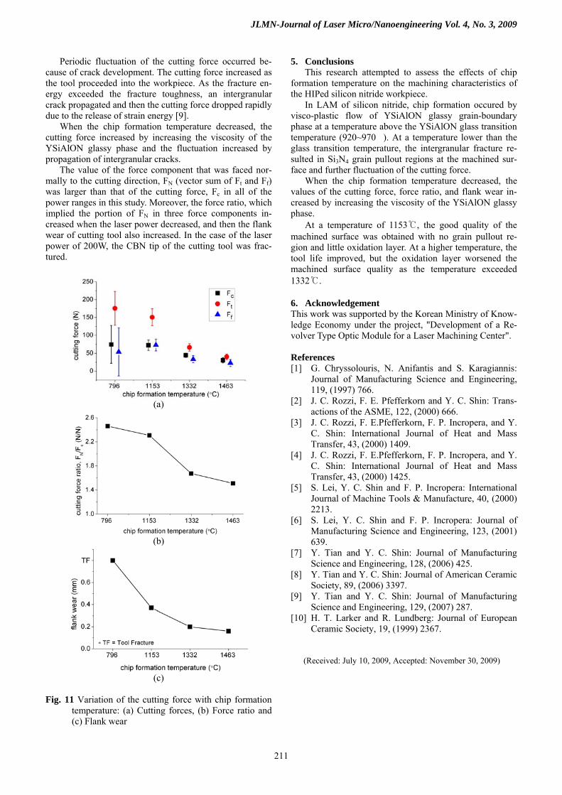
Fig. 11 shows the variation of the cutting forces and flank wear with various laser powers. The cutting force data between 10 and 30 seconds was averaged to exclude the effect of flank wear and tool fracture. Error bars present the fluctuation of the cutting force.
(a) (b)
(c) (d)
Fig. 9 Optical micrographs of chip with various chip for-
mation temperature: (a) 796℃, (b)1153℃, (c) 1332℃ and (d) 1463℃
(a) (b)
(c) (d)
Fig. 10 SEM micrographs of chip with various chip forma-
tion temperature: (a) 796℃, (b)1153℃, (c) 1332℃ and (d) 1463℃
JLMN-Journal of Laser Micro/Nanoengineering Vol. 4, No. 3, 2009
211
Periodic fluctuation of the cutting force occurred be-cause of crack development. The cutting force increased as the tool proceeded into the workpiece. As the fracture en-ergy exceeded the fracture toughness, an intergranular crack propagated and then the cutting force dropped rapidly due to the release of strain energy [9].
When the chip formation temperature decreased, the cutting force increased by increasing the viscosity of the YSiAlON glassy phase and the fluctuation increased by propagation of intergranular cracks.
The value of the force component that was faced nor-mally to the cutting direction, FN (vector sum of Ft and Ff) was larger than that of the cutting force, Fc in all of the power ranges in this study. Moreover, the force ratio, which implied the portion of FN in three force components in-creased when the laser power decreased, and then the flank wear of cutting tool also increased. In the case of the laser power of 200W, the CBN tip of the cutting tool was frac-tured.
(a)
(b)
(c)
Fig. 11 Variation of the cutting force with chip formation
temperature: (a) Cutting forces, (b) Force ratio and (c) Flank wear
5. Conclusions This research attempted to assess the effects of chip
formation temperature on the machining characteristics of the HIPed silicon nitride workpiece.
In LAM of silicon nitride, chip formation occured by visco-plastic flow of YSiAlON glassy grain-boundary phase at a temperature above the YSiAlON glass transition temperature (920~970�). At a temperature lower than the glass transition temperature, the intergranular fracture re-sulted in Si3N4 grain pullout regions at the machined sur-face and further fluctuation of the cutting force.
When the chip formation temperature decreased, the values of the cutting force, force ratio, and flank wear in-creased by increasing the viscosity of the YSiAlON glassy phase.
At a temperature of 1153℃, the good quality of the machined surface was obtained with no grain pullout re-gion and little oxidation layer. At a higher temperature, the tool life improved, but the oxidation layer worsened the machined surface quality as the temperature exceeded 1332℃.
6. Acknowledgement This work was supported by the Korean Ministry of Know-ledge Economy under the project, "Development of a Re-volver Type Optic Module for a Laser Machining Center". References [1] G. Chryssolouris, N. Anifantis and S. Karagiannis:
Journal of Manufacturing Science and Engineering, 119, (1997) 766.
[2] J. C. Rozzi, F. E. Pfefferkorn and Y. C. Shin: Trans-actions of the ASME, 122, (2000) 666.
[3] J. C. Rozzi, F. E.Pfefferkorn, F. P. Incropera, and Y. C. Shin: International Journal of Heat and Mass Transfer, 43, (2000) 1409.
[4] J. C. Rozzi, F. E.Pfefferkorn, F. P. Incropera, and Y. C. Shin: International Journal of Heat and Mass Transfer, 43, (2000) 1425.
[5] S. Lei, Y. C. Shin and F. P. Incropera: International Journal of Machine Tools & Manufacture, 40, (2000) 2213.
[6] S. Lei, Y. C. Shin and F. P. Incropera: Journal of Manufacturing Science and Engineering, 123, (2001) 639.
[7] Y. Tian and Y. C. Shin: Journal of Manufacturing Science and Engineering, 128, (2006) 425.
[8] Y. Tian and Y. C. Shin: Journal of American Ceramic Society, 89, (2006) 3397.
[9] Y. Tian and Y. C. Shin: Journal of Manufacturing Science and Engineering, 129, (2007) 287.
[10] H. T. Larker and R. Lundberg: Journal of European Ceramic Society, 19, (1999) 2367.
(Received: July 10, 2009, Accepted: November 30, 2009)