laser drilling for electrical interconnection in advanced...
TRANSCRIPT

Laser Drilling For Electrical Interconnection in Advanced Flexible Electronics Applications
Timothy E AntesbergerEndicott Interconnect Technologies1093 Clark StreetEndicott, NY [email protected]
Acknowledgement:Frank Egitto
Outline
Introduction: Motivation for laser processing and advanced electronics
Laser Fundamentals
Laser/Material Interactions
Types of lasers, laser drilling systems, and drilling techniques
Laser-enabled high-performance electronic components
Extensions of laser processing technologies

Levels of Interconnection
Functions of Rigid and Flexible Electronic PackagingMounting and physical support of electronic components
Protection of devices from environment
Removal of heat from devices
Electrical interconnection of components
Signal distributionPower distribution
Chip
Chip Carrier
Underfill
Conductive Joint
Flip Chip Assembly
Chip
Chip Carrier
EncapsulantWire
Wirebond Assembly
Flex
Wafer
IC Chip
System

Traditional Application of Laser Processing to Flexible Electronics
Annealing of conductors to control electrical properties
LPKF
Exposure of photosensitive materials (e.g., photoresists) for pattern formation
Holemaking for electrical interconnection
SkivingLabeling
SingulationRepair of circuit traces
etc.

Layer 1
Layer 2
Copper Lines Copper Pads
High density elecronic components arecomposed of multiple layers of circuit traces.

A
A'
Land
Plated Through Hole (PTH)
Electrical interconnection between layersis made with drilled and plated holes.
Wiring Planes
External Mounting Planes(No Wiring)

Tycom Microdrills 550 — Diameters .0040" - .0130"
For decades, mechanical drilling has been the conventional means of hole formation and is still a mainstay for most printedcircuit board applications.
Hold down ring
Die
Punch
Mechanical punching has been used extensively for hole formation in thin, flexible, homogeneous materials. Hole diameters on the order 0.002" are achievable, but the process ishighly sensitive to material properties.
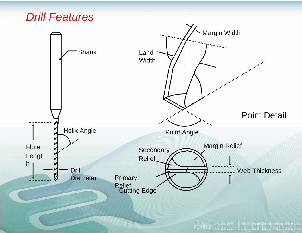
FluteLength
Helix Angle
Drill Diameter
Shank
Cutting Edge
Margin Width
Point Angle
Land Width
Web Thickness
Margin Relief
Primary Relief
Secondary Relief
Drill Features
Point Detail

The demand for high-performance, lightweight, portable computing power is driving the industry toward miniaturization of many electronic products and the components that comprise them.
Common examples are laptop computerspersonal digital assistantsdigital camerascellular phones
"Smaller, Lighter, Faster, Cheaper"


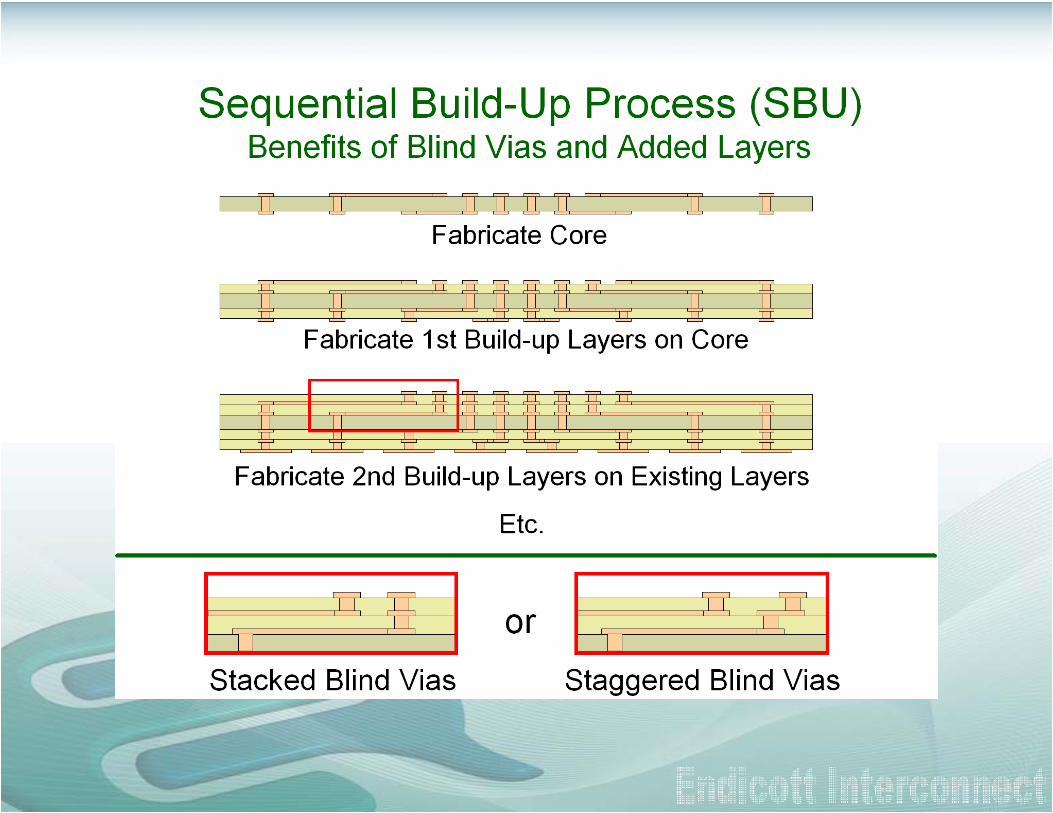
Traditional Approaches to Increasing Circuit Density
Smaller lines and spacesSmaller viasBlind and buried (controlled-depth) viasAdded wiring layers
A
A'Use of blind vias increases wiring density.
A
A'
A'
Adding layers increases wiring density
A
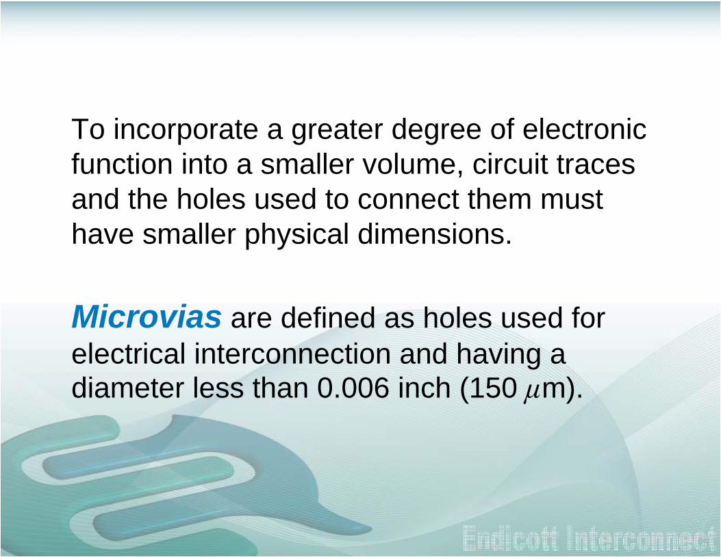
To incorporate a greater degree of electronic function into a smaller volume, circuit traces and the holes used to connect them must have smaller physical dimensions.
Microvias are defined as holes used for electrical interconnection and having a diameter less than 0.006 inch (150 m).

hole diameter, dcapture pad diameter, c = d + xline width, lline space, sline-to-pad space, phole pitch, h
d + xd
p
ls
hk
Top View
CrossSection
B
B'
A
A'
2 Lines Per Channel
Hole diameters affect wiring density.

h1
Increased Number of Lines Per Channel
Increase in Wiring DensityWith Reduction in Hole Diameter
h2
h1
Reduced PitchLand on larger hole
Land on smaller hole

Top View
hole diameter, dcapture pad diameter, c = d + xline width, lline space, sline-to-pad space, phole pitch, h
Cross Section

Hole Diameter and Wiring DensitHole Diameter and Wiring Density


Increase in wiring density with decrease in hole diameter by way ofincreased number of lines per channel (pitch constant).
For h, p, x, l, and s, constant,
h = nl + (n -1)s + 2p + x + dn(l + s) = - d + q , where q = h + s - 2p - x
n2(l + s) = - d2 + q , where d2 is the smaller diameter hole
n1(l + s) = - d1 + q , where d1 is the larger diameter hole
(n2 -n 1)(l + s) = d1 - d2
n2 - n1 = (d1 - d2) / (l + s).
That is, the increase in the number of lines per channel, n2 - n1 , is equal to the ratio of thechange in hole diameter, d1 - d2 , to the line pitch, l + s. Again, n2 - n1 must be an integer. Forexample, if d1 - d2 < l + s , there is no increase in wiring density. If (l + s) < (d1 - d2) < 2(l + s) ,lines per channel increase by 1. If 2(l + s) < (d2 - d1) < 3(l + s), lines per channel increase by 2,and so on.

B
B'
A
A'
2 Lines Per Channel
PTHs consume real estate, blockingchannels that could be used for wiring.
Cross Section

B
B'
A
A'C'
B
B'
A
A'
PTHBlind Via
Space available for wiring
Increase In Wiring Density With Blind Vias

Increase In Wiring Density Blind Via vs PTH
Use of blind vias Increases wiring density.
Mechanical drills and punches are not suited to formation of blind microvias.
A
AA'
A'

blind via through via
buried via
Microvia
A blind, buried, or through via that is on the order of 150 m or smaller in diameter.
Definition often limited to blind vias for high density interconnect structures (HDIS).

Layer Interconnection with Controlled-Depth Vias
Layer Interconnection with Plated Thru Holes Lines must go around PTH's
Controlled-depth vias don't block lines
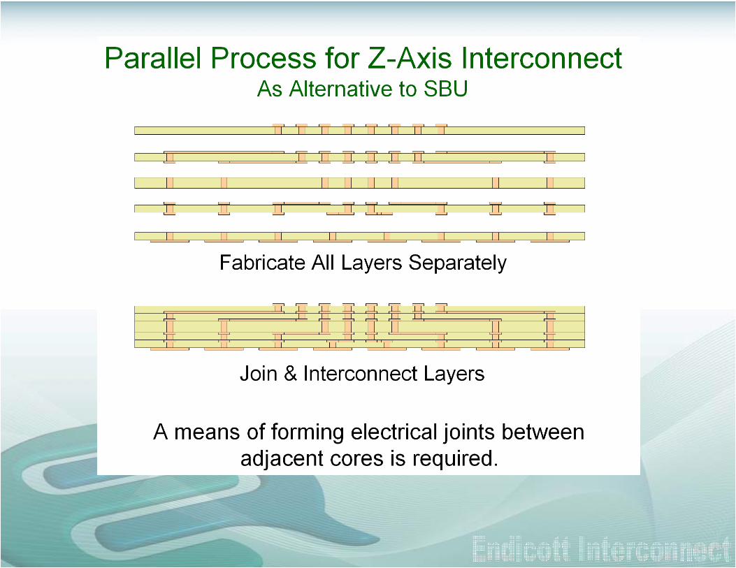

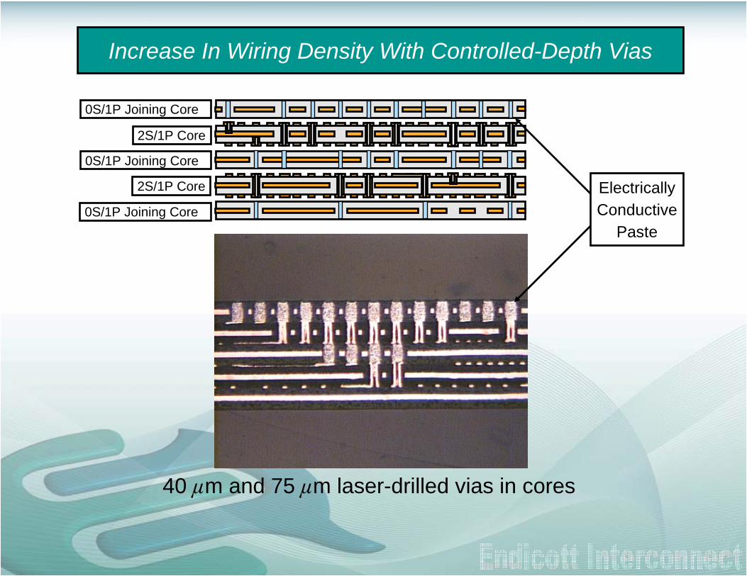
Increase In Wiring Density With Controlled-Depth Vias
40 m and 75 m laser-drilled vias in cores
0S/1P Joining Core
2S/1P Core
0S/1P Joining Core
2S/1P Core
0S/1P Joining Core
Electrically Conductive
Paste
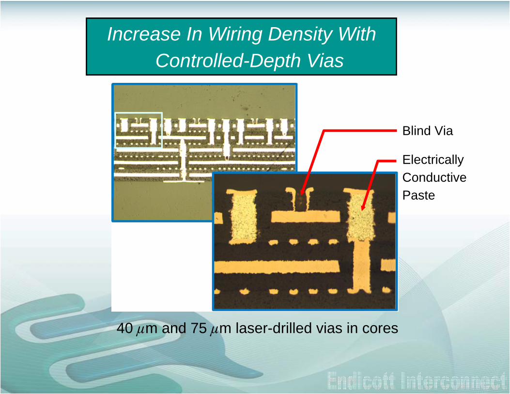
Increase In Wiring Density WithControlled-Depth Vias
Blind Via
ElectricallyConductivePaste
40 m and 75 m laser-drilled vias in cores

Mechanically-Drilled Through Via75 m diameter
170 m clearance hole
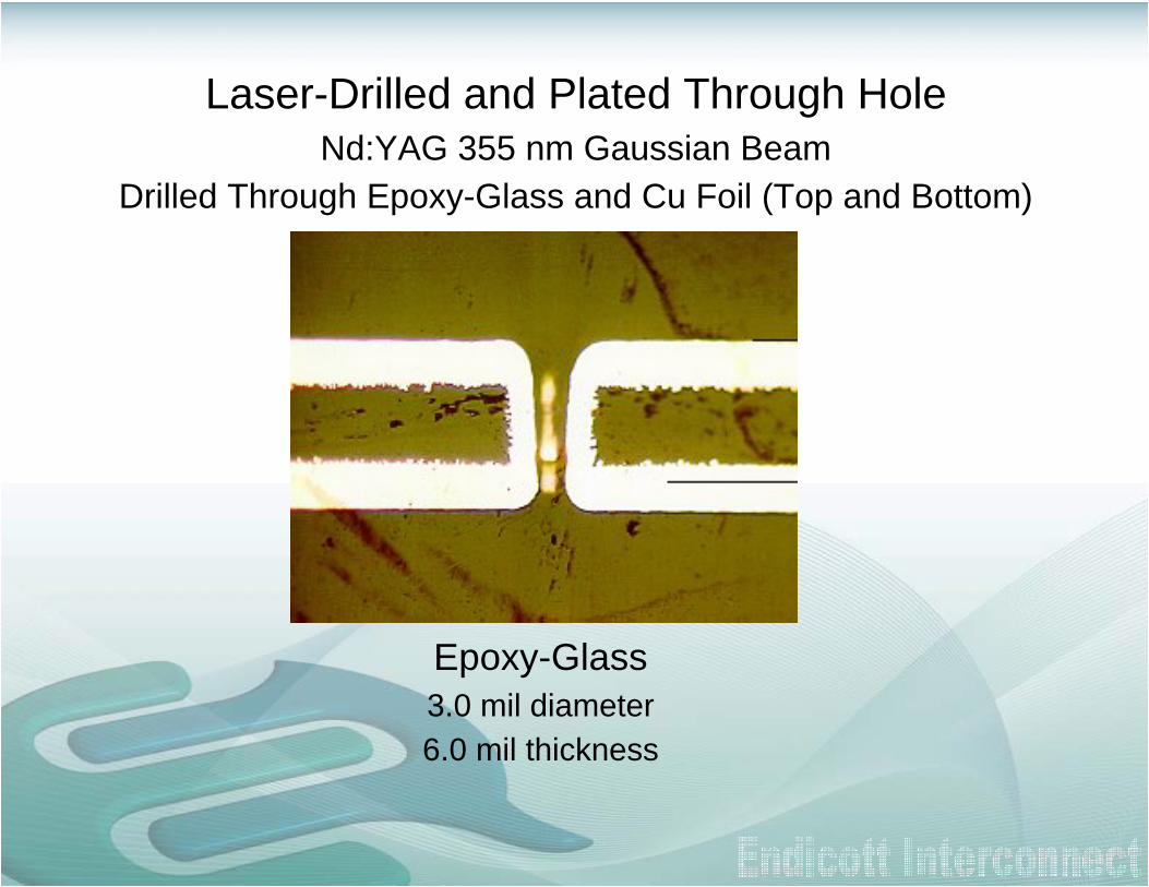
Laser-Drilled and Plated Through HoleNd:YAG 355 nm Gaussian Beam
Drilled Through Epoxy-Glass and Cu Foil (Top and Bottom)
Epoxy-Glass3.0 mil diameter6.0 mil thickness
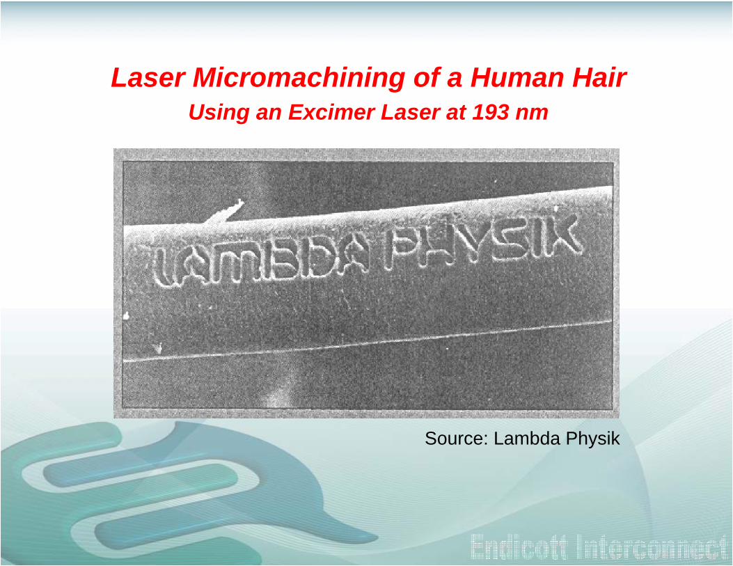
Laser Micromachining of a Human HairUsing an Excimer Laser at 193 nm
Source: Lambda Physik
Outline
Introduction: Motivation for laser processing in advanced electronics
Laser Fundamentals
Laser/Material Interactions
Types of lasers, laser drilling systems, and drilling techniques
Laser-enabled high-performance electronic components
Extensions of laser processing technologies

Lasing MediumR=100%
R<100%
1
2
3
4
6
5
LLight ight AAmplification by mplification by SStimulated timulated EEmission of mission of RRadiationadiation
Source: Engineering Technology Institute

Laser Wavelengths For Processing
100 nm
Excimer Nd:YAG CO2
Laser Type
Wavelength
248 nm 1064 nm
VISIBLE INFRAREDULTRAVIOLET
1000 nm 10,000 nm
400 nm 750 nm
10,600 nm

Lasing MediumLasing Medium
Pumping MechanismPumping Mechanism
MirrorMirrorR = R = 100%100%
MirrorMirrorR < R < 100%100%
Laser Beam OutLaser Beam Out
Elements of a Elements of a LaserLaser
IntenseIntenseMonochromaticMonochromatic
Continuous Wave (CW) or Pulsed (High Energy Bursts) Outputs
Pulsed Mode Used For Clean Holemaking With a Minimum of Thermal Damage

Outline
Introduction: Motivation for laser processing in advanced electronics
Laser Fundamentals
Laser/Material Interactions
Types of lasers, laser drilling systems, and drilling techniques
Laser-enabled high-performance electronic components
Extensions of laser processing technologies
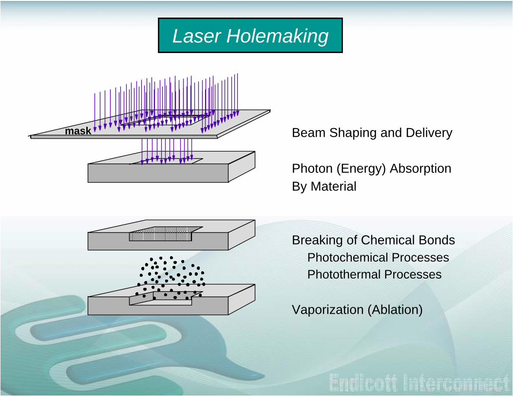
mask Beam Shaping and Delivery
Photon (Energy) Absorption By Material
Breaking of Chemical BondsPhotochemical ProcessesPhotothermal Processes
Vaporization (Ablation)
Laser Holemaking
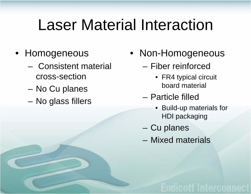
Laser Material Interaction
• Homogeneous– Consistent material
cross-section – No Cu planes – No glass fillers
• Non-Homogeneous– Fiber reinforced
• FR4 typical circuit board material
– Particle filled• Build-up materials for
HDI packaging
– Cu planes– Mixed materials

200 400 600 800 1000 1200
Wavelength (nm)
00.10.20.30.40.50.60.70.80.9
1
AbsorptionFR4Matte CuGlass
355 nm - Nd:YAG 3rd Harmonic
308 nm - XeCl excimer
248 nm - KrF excimer
532 nm - Nd:YAG 2nd Harmonic
1064 nm - Nd:YAG Fundamental
Source: ESI
Absorption Curves

Focused Spot
Laser Beam Delivery
Mask Imaging
Mask
Contact or Conformal Mask
Lens
EtchedMetalFoil
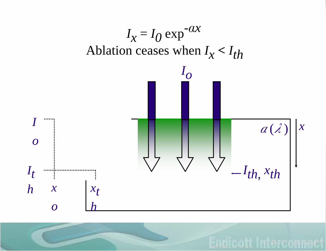
Io
Ith, xth
( )
Ix = I0 exp- x
Ablation ceases when Ix < Ith
Io
Ith x
oxth
x

shallow absorption moderate absorption deep absorption
Ix = I0 exp- x
I0 = I1 I0 = I2 > I1 I0 = I3 > I2
Rate(Etched Depth Per Pulse)
I1 I2 I3 I0

moderate deeper absorptionhigh rate
low little or no absorptionlow rate
Ix = I0 exp- x
1 2 3
high strong but shallow absorptionlow rate
321
I0 I0 I0
Rate(Etched Depth Per Pulse)
Ith = k (1/ n)
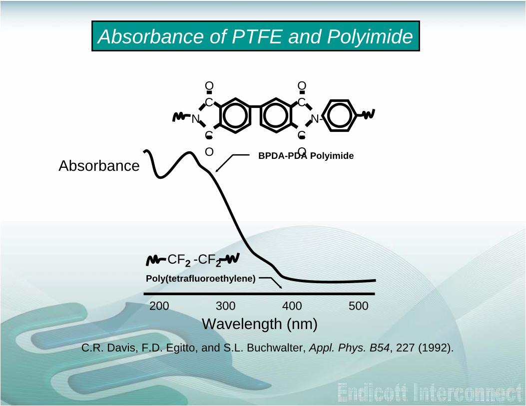
200 300 400 500
BPDA-PDA Polyimide
CF2 -CF2Poly(tetrafluoroethylene)
OC
N-CO
OC
NCO
Absorbance
Wavelength (nm)
Absorbance of PTFE and Polyimide
C.R. Davis, F.D. Egitto, and S.L. Buchwalter, Appl. Phys. B54, 227 (1992).

PTFE
0.1 1 10 100% Polyimide in PTFE
0
1
2
3
4
5
Etch Rate (um/pulse)
BPDA-PDA Polyimide
Doping of PTFE With Polyimide
F.D. Egitto and C.R. Davis, Appl. Phys. B55, 488 (1992).
~ 102 cm-1
OC
CO
N
OC
CO
N
CF2 -CF2
~ 105 cm-1
Outline
Introduction: Motivation for laser processing and advanced electronics
Laser Fundamentals
Laser/Material Interactions
Types of lasers, laser drilling systems, and drilling techniques
Laser-enabled high-performance electronic components
Extensions of laser processing technologies
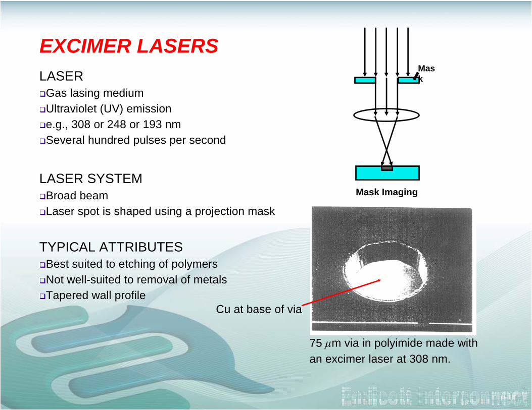
EXCIMER LASERSLASER
Gas lasing mediumUltraviolet (UV) emissione.g., 308 or 248 or 193 nmSeveral hundred pulses per second
LASER SYSTEMBroad beamLaser spot is shaped using a projection mask
TYPICAL ATTRIBUTESBest suited to etching of polymersNot well-suited to removal of metalsTapered wall profile
75 m via in polyimide made with an excimer laser at 308 nm.
Mask Imaging
Mask
Cu at base of via

Excimer Laser
Turning Mirror
Turning Mirror
Turning Mirror
Prism Beam ExpanderBeam Homogenizer
Lens
Objective Lens
Vacuum Chuck / Rotational StageX-Y Positioning Stage
Substrate
Mask
Example of Excimer Laser SystemExample of Excimer Laser SystemUsed With Projection MaskUsed With Projection Mask
Mask Imaging
Mask
x
y
stationary

Excimer Laser
Turning Mirror
Turning Mirror
Turning Mirror
Prism Beam ExpanderBeam Homogenizer
Lens
Objective Lens
Vacuum Chuck / Rotational StageX-Y Positioning Stage
Substrate
Mask
Example of Excimer Laser SystemExample of Excimer Laser SystemUsed With Projection MaskUsed With Projection Mask
Stationary Beam, Scanning Mask and SubstrateStationary Beam, Scanning Mask and Substrate
Mask Imaging
Mask
x
x

Excimer Laser
Turning Mirror
Turning Mirror
Turning Mirror
Prism Beam ExpanderBeam Homogenizer
Lens
Objective Lens
Vacuum Chuck / Rotational StageX-Y Positioning Stage
Mo MaskSubstrate
Example of Excimer Laser SystemExample of Excimer Laser SystemUsed With Contact MaskUsed With Contact Mask
Contact or Conformal Mask
Lens
Etched Metal Foil
y
x

LASERGas Lasing MediumIR emission (around 10.6 m)
LASER SYSTEMFocused beam (50-75 m minimum diameter) or metal contact mask
TYPICAL ATTRIBUTESHighest powerBest suited to drilling of polymers, some thermal damageHigh reflectance from metal surfacesBest when speed (not small size) is importantUsed in about 80% of microvia applications
CO2 LASERS
Focused Spot Contact or Conformal Mask
Lens
EtchedMetalFoil
CO2 Laser Processing of Woven Glass/Epoxy Resin Using a Conformal Mask. Cu-Plated 6 mil Via.

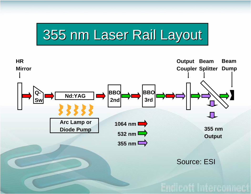
LASERSolid Lasing MediumInfrared (IR) Fundamental Emission (1064 nm)Visible (532 nm) or UV (355 or 266 nm) emission with nonlinear crystalsUp to 100,000 pulses per second
LASER SYSTEMFocused beam (12 to 25 m diameter, depending on wavelength and optics) or shaped beam for blind via drilling.Trepanning for holes having diameters greater than beam diameter
TYPICAL ATTRIBUTESCapable of drilling variety of materials (polymers, glass, metals)Most versatileWell-suited to holes with small diameter, high aspect ratioUsed in about 20% of microvia applications
Nd:YAG LASERS
Mask Imaging
Mask
Focused Spot
Trepanning
Top View
Beam
Via
Punching
Nd:YAGQ-Sw
BBO2nd
BBO3rd
Arc Lamp orDiode Pump
OutputCoupler
BeamSplitter
BeamDump
355 nmOutput
1064 nm
532 nm
355 nm
HRMirror
355 nm Laser Rail Layout355 nm Laser Rail Layout
Source: ESI
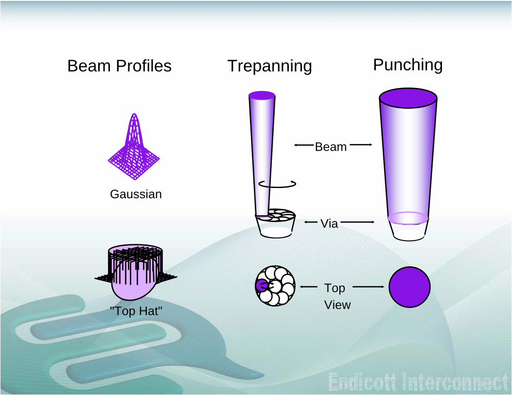
Trepanning
Top View
Beam
Via
PunchingBeam Profiles
Gaussian
"Top Hat"

Radial Pitch
Beam Diameter
Bite Size
Spiral Tool
Beam Diameter
Bite Size
Trepan Tool
multiple revolutions(programmable) laser beam turns
on and off


Beam PositioningBlind Via DrillingThrough Via Drilling

Blind via on pad
Buried via throughclearance hole
Registration Requirements
Clearance hole

Panel BorderToolpath File Border
Design Data Locations Drilled Hole
Locations
Four Point AlignmentToolpath File %(ESI 5100)T1 8T0 996 G0X112710.0 Y94580.0X112710.0 Y661160.0X504510.0 Y661160.0X504510.0 Y94580.0
T1 1T0 101 G0T2 101.6X71119.0 Y80690.0Y83230.0Y85770.0Y88310.0Y90850.0X80010.0 Y89580.0X78739.0 Y80690.0X76199.0X73659.0X81279.0X118109.0 Y88310.0X72389.0 Y128950.0X214629.0 Y88310.0X237490.0 Y89580.0X261644.9 Y102852.0Y104122.0Y105392 0
Designed location of alignment markers
Designed location of drilled holes
Hole Diameter in m
Design Alignment Targets
Measured Alignment Targets

RegistrationX-Ray Image of 75 m Vias Through 125 m Clearance Holes
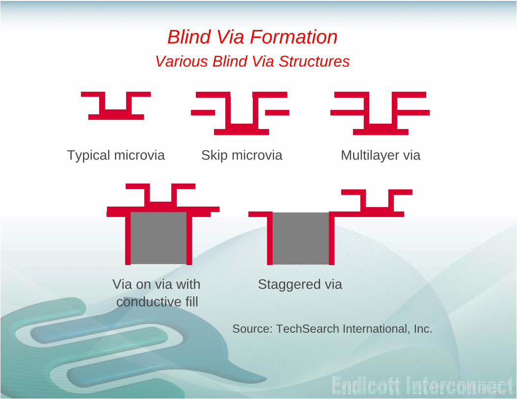
Typical microvia Multilayer viaSkip microvia
Via on via withconductive fill
Staggered via
Blind Via FormationVarious Blind Via Structures
Source: TechSearch International, Inc.

Dielectric
Mask Imaging
Mask
Focused Spot
Contact or Conformal Mask
Lens
EtchedMetalFoil
Blind Via Drilling:
Cu surface mask
or, without Cu mask
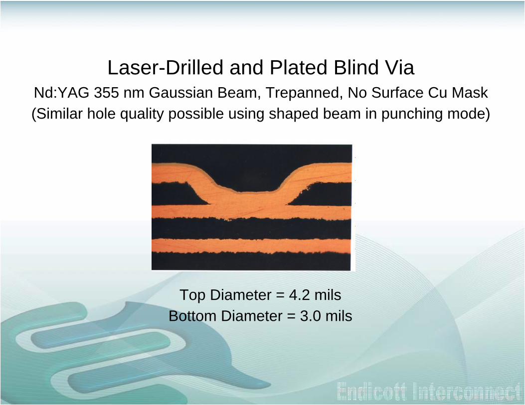
Laser-Drilled and Plated Blind ViaNd:YAG 355 nm Gaussian Beam, Trepanned, No Surface Cu Mask(Similar hole quality possible using shaped beam in punching mode)
Top Diameter = 4.2 milsBottom Diameter = 3.0 mils

In Focus, High Fluence*For High Intensity
Through Metal Stop on Metal
Out of Focus or ORLow Fluence For Low Intensity
"Shaped" UV orIR to Reflect From Metal
* fluence = energy per unit area per pulse
Control of Etch Selectivity By Adjustment of Fluence or Wavelength

Pass 1: Remove surface Cu.
Nd:YAG Laser.........Two-Pass ProcessGaussian Beam Profile
Trepan or Spiral
Pass 2: Remove dielectric.
Trepan or Spiral

160 m Laser-Drilled Blind Via In Epoxy/GlassUsing 355 nm Nd:YAG Gaussian Beam
Spiral Mode, Two Pass Process

CO2 Laser..........Two-Step Process Chemically etched copper "mask"
Ablate dielectric with IR beam

Combination Nd:YAG & CO2 Laser Process
Trepan or Spiral

UV UV
Cu Pad
Apply
Expose
Develop
Photomask
Photosensitive Dielectrics
Positive Negative

UV UV
Cu PadPositive Photoresist Negative Photoresist
Apply Resist
Expose
Develop
Photomask
Photolithography

O* CO, CO 2, etc.
Plasma Wet Chemical
Chemical Etching
Photoresist
Immerse In or Spray WithWet Chemical Etchant
Strip Photoresist
Plasma Etch
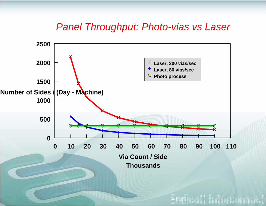
0 10 20 30 40 50 60 70 80 90 100 110
ThousandsVia Count / Side
0
500
1000
1500
2000
2500
Number of Sides / (Day - Machine)
Laser, 300 vias/secLaser, 80 vias/secPhoto process
Panel Throughput: Photo-vias vs Laser

50,000 100,000
150,000 200,000
250,000
Number of Vias Per Panel
Cost Per Panel
Laser
Plasma
Laser Drilling vs Plasma EtchingRelative Cost

0.002" 0.004" 0.006" 0.008" 0.010"
Via Diameter
Cost Per ViaLaserMechanical
Laser Drilling vs Mechanical DrillingRelative Cost

Photo-via42.0%
Laser via43.0%
Plasma3.0%
Drill9.0% Punch
3.0%
December 19961
Photo-via34.0%
Laser via60.0%
Plasma1.0%
Drill4.0% Punch
1.0%
August, 19981
1Estimates: N.T. Information, Ltd., charts courtesy of Electro Scientific Industries.
2The Electronics Industry Report 2002, Prismark Partners LLC.
Packaging and HDI Production
Laser vias used for 90% of HDI applications in 2002.2

0 2 4 6 8 10 12 14Via Diameter (mils)
0.1
1
10
Aspect Ratio
Source: Electro Scientific Industries, Inc.
ESI's Via Technology Roadmap
UVYAG
MechanicalDrill
Blind Vias Through Vias
CO2Photovia

Outline
Introduction: Motivation for laser processing and advanced electronics
Laser Fundamentals
Laser/Material Interactions
Types of lasers, laser drilling systems, and drilling techniques
Laser-enabled high-performance electronic components
Extensions of laser processing technologies

HyperBGAHyperBGAR
90 m Blind Via
Chip
Solder Underfill
50 m Through Via

Standard Build-up 3-2-3CoreEZ 2-4-2
X Section Comparison
Both packages use 50υ blind viasCoreEZ core vias are 4x smallerCoreEZ is ½ as thickCore EZ’s core is 6 times as denseCoreEZ can fully route signals on both sides of the core
2 times the wiring density with fewer layers
CoreEZCoreEZ R

HyperZ
• Coreless structures for maximum wiring density– 40um and 65um vias
R

R. Fillion, E. Delgado, P. McConnelee, and R. Beaupre, "A High Performance Polymer Thin Film Power Electronics Packaging Technology," Advancing Microelectronics, 30(5), 7 (2003).
GE Power Overlay
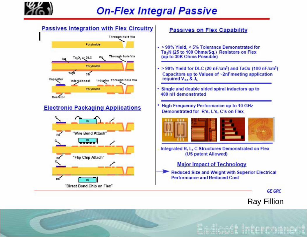
Ray Fillion

Outline
Introduction: Motivation for laser processing and advanced electronics
Laser Fundamentals
Laser/Material Interactions
Types of lasers, laser drilling systems, and drilling techniques
Laser-enabled high-performance electronic components
Extensions of laser processing technologies

Embedded Resistor Trimming
• Resistors formed through etching thin film resistor foil
• Resistor value designed low for etching process
• Laser used to trim up to nominal value
• Tighter control

Laser Direct Imaging
• Laser Direct Imaging of Photoresist– Real-time registration adjustment– Mask savings v. traditional photoprocessing– Falls inline with existing equipment infastructure
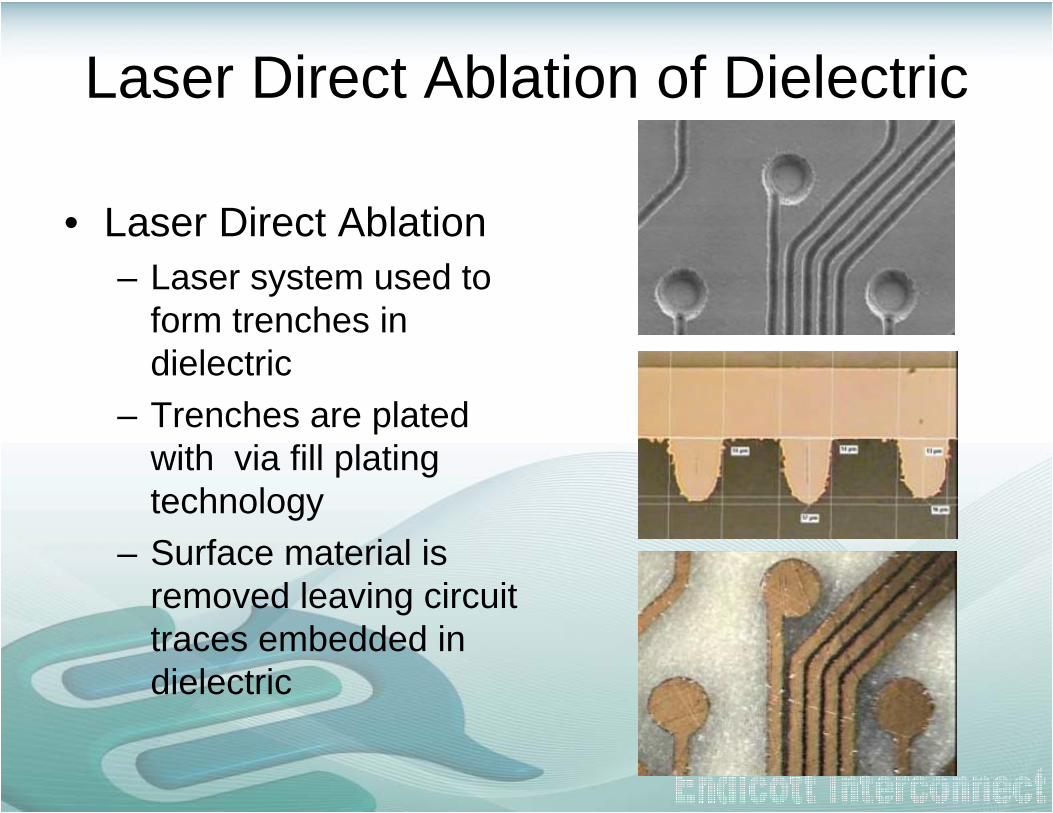
Laser Direct Ablation of Dielectric
• Laser Direct Ablation– Laser system used to
form trenches in dielectric
– Trenches are plated with via fill plating technology
– Surface material is removed leaving circuit traces embedded in dielectric
SummaryLaser processing is key to providing portable and high performance computing power.
Technology is changing rapidly with new enabling applications being consistently being discovered.
Abundant opportunity for process control through variation of laser beam parameters (e.g., wavelength and fluence) and material properties.
Thanks for your attention.QUESTIONS?