laser micromachining fabrication of thz components · laser micromachining fabrication of thz...
TRANSCRIPT
Laser Micromachining Fabrication of THz Components
C. Drouët d’Aubigny, C. Walker, B. Jones, C. Groppi Steward Observatory, Univ. of Arizona.
J. Papapolymerou, C. Tavernier
Dept. of Electrical and Computer Engineering, Univ. of Arizona.
ABSTRACT
Laser micromachining techniques can be used to fabricate high-quality waveguide structures and quasi-optical components to micrometer accuracies. Successful GHz designs can be directly scaled to THz frequencies. We expect this promising technology to allow the construction of the first fully integrated THz heterodyne imaging arrays. At the University of Arizona, construction of the first laser micromachining system designed for THz waveguide components fabrication has been completed. Once tested and characterized our system will be used to construct prototype THz 1x4 focal plane mixer arrays, magic tees, AR coated silicon lenses, LO source phase gratings, filters and more. Our system can micro-machine structures down to a few microns accuracy and up to 6 inches across in a short time. This paper discusses the design and performance of our micromachining system, and illustrates the type, range and performance of components this exciting new technology will make accessible to the THz community.
INTRODUCTION Laser micro chemical etching works by focusing several watts of laser power on a silicon wafer in a low-pressure chlorine ambient (200 Torr). The deposited energy vaporizes a cylindrical region 6 µm wide and 1 µm deep. The vaporized silicon atoms react immediately with chlorine molecules to form silicon tetrachloride, which is gaseous at the pressure used and prevents re-deposition on the substrate (see Figure 1). Melted silicon not captured by chlorine re-deposits epitaxially as soon as the beam is moved to a different position. Laser micro machining possesses a significant edge over conventional techniques. It does not require the use of masks, and is not confined to any given crystal plane. Since it is a non-contact process, laser micro machining eliminates tool wear and vibration. The etch depth is only limited by the motion range (5mm) of the vertical stages. The laser micromachining process is entirely computer controlled and permits proven complex waveguide designs and quasi-optical components to be scaled to THz frequencies. The system also allows fast prototyping: the magic tee structure presented in this paper took

less than 5 minutes to etch. Larger complex structures such as corrugated feedhorns may take up to 1 hour of actual machining time. Generally, the complexity of the structure has little impact, if any, on the process time. In practice, only the size and volume of the region to be etched have a meaningful impact, making this process ideally suited for THz applications.
Figure 1-a (left), 1-b (right): a) The focused spot of a laser is scanned across a silicon wafer. Silicon atoms are vaporized, and immediately react with the ambient chlorine molecules preventing re-deposition. Using high numerical aperture optics confines the etch to a region only a few micrometers wide. The trade- off of high NA is a tapering of the beam that can be significant for some applications, eg. vertical walls (Ted Bloomstein, MIT, Ph-D Thesis). b) The Gaussian beam behavior of the laser beam provides a 100 µm deep region where vertical walls can be machined without significant loss in resolution. The system we have built at Steward Observatory (Fig. 3) is equipped with a 30W, water-cooled, Argon Ion, laser used at 488 and 514nm. While only 4W is actually required on the sample, system losses, and the need to stop the laser to a small aperture to obtain a TEM00 Gaussian beam, increase the laser power requirements. The beam waist diameter when focused on the silicon is ~6µm. The F/# of the system is 5, causing a beam taper angle of 6° and an aspect ratio of 10:1. However, in the 100 µm focal region of the laser, vertical walls with an extremely high aspect ratio can be achieved. The currently available scanning range is ~ 5 x 5 mm. Through the use of stitching, structures up to 150 mm in diameter can be machined. In our design, the laser beam is expanded to 16mm. The beam is then deflected by a commercial X-Y galvo-mirror scanner onto an achromatic scanning lens. The focused beam is then introduced through a fused silica window into a stainless steel reaction chamber containing the silicon substrate (see Fig.2). The wafer surface temperature is biased to roughly 100°C using a parabolic IR illumination source shining through a second window on the backside of the reaction chamber (see Fig 2). The process is monitored through the focusing optics using a CCD with a plate scale of 7 µm per pixel. The scanning system is driven directly from computer-generated patterns, which can be
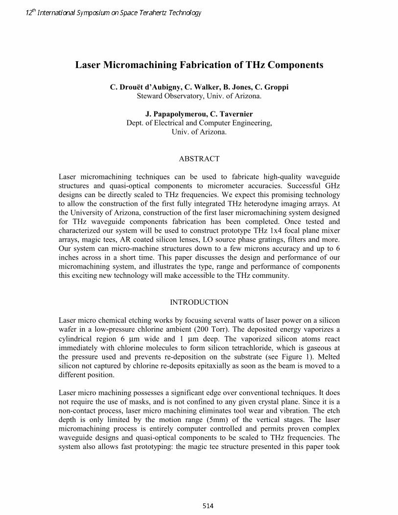
constructed using Autodesk's AutoCAD. The ensemble is mounted on computer controlled X-Y-Z precision motion stages (see Fig. 3) allowing the stitching of large structures.
Figure 2: The laser micro machining optical hood. The Argon-Ion laser is visible in the back. On the right side of the image, the beam can be seen reflecting off relay mirrors, passing through the electronic shutter and beam expander. The beam-splitter, wave-plates and CCD camera labeled on the image are not visible from this angle. The open reaction chamber loaded with a silicon wafer can be seen. The entire assembly is mounted on precision motion stages. Before operation the cell is evacuated, then filled with 99.9 % pure chlorine gas to 100 Torr. After ~2 hours of machining the remaining chlorine gas and silicon chlorides are captured in a scrubbing bubbler. Figure 4 shows the system in our laboratory. The chlorine and nitrogen gas cylinders are stored in the gas cabinet on the right. The central hood houses the laser, reaction chamber, and optics. The vacuum pump and chlorine scrubbers are contained in the small gas cabinet on the left.
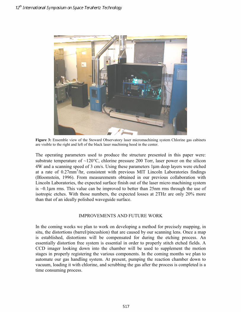
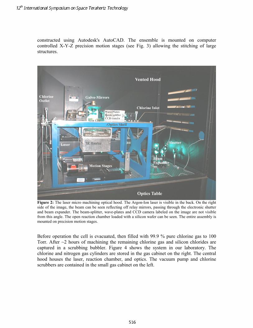
Figure 3: Ensemble view of the Steward Observatory laser micromachining system Chlorine gas cabinets are visible to the right and left of the black laser machining hood in the center. The operating parameters used to produce the structure presented in this paper were: substrate temperature of ~120°C, chlorine pressure 200 Torr, laser power on the silicon 4W and a scanning speed of 3 cm/s. Using these parameters 1µm deep layers were etched at a rate of 0.27mm3/hr, consistent with previous MIT Lincoln Laboratories findings (Bloomstein, 1996). From measurements obtained in our previous collaboration with Lincoln Laboratories, the expected surface finish out of the laser micro machining system is ~0.1µm rms. This value can be improved to better than 25nm rms through the use of isotropic etches. With those numbers, the expected losses at 2THz are only 20% more than that of an ideally polished waveguide surface.
IMPROVEMENTS AND FUTURE WORK In the coming weeks we plan to work on developing a method for precisely mapping, in situ, the distortions (barrel/pincushion) that are caused by our scanning lens. Once a map is established, distortions will be compensated for during the etching process. An essentially distortion free system is essential in order to properly stitch etched fields. A CCD imager looking down into the chamber will be used to supplement the motion stages in properly registering the various components. In the coming months we plan to automate our gas handling system. At present, pumping the reaction chamber down to vacuum, loading it with chlorine, and scrubbing the gas after the process is completed is a time consuming process.

We also plan to improve the opening and closing mechanism of the reaction chamber. and design a better, wider, scanning lens that will permit the production of structures up to 30mm in diameter without stitching. Finally, we are interested in exploring etching parameter space to get higher removal rates and smaller etch depths.
APPLICATIONS OF LASER MICROMACHINED DEVICES Laser micromachining permits the direct scaling of successful waveguide and quasi-optical components to THz frequencies. The process works best for structures that can be machined directly onto a 2-dimensional surface. For example, `split-block' waveguide components and anti-reflection (AR) grooves are well adapted for fabrication with this process. Here we discuss three specific examples of laser machined components, waveguide magic-Tee's, feedhorns, and AR coatings. These components are needed at THz frequencies to enable the construction of efficient receiver systems for space and airborne astronomy as well as space-based communication systems. 1. Magic-Tee The magic tee is a four-port network in which an incident signal on any one port divides between two output ports with the remaining port being isolated. The magic tee has been used primarily at microwave frequencies in a number of applications, including coherent power combining and balanced mixers. Figure 4 is a schematic of a basic waveguide magic tee.
Figure 4: Schematic of magic tee structure (Rizzi, 1988). If the E-arm (Port 3) is match terminated, then signals incident at Ports 1 and 2 will be isolated from each other and combine in phase at Port 4 (Rizzi 1988). This configuration of a magic tee could be used to coherently combine the local oscillator power from 2 or more independent sources or as the heart of a coherent beam combiner for space interferometry missions.
The match termination for this application can be achieved in silicon using the design shown in Figure 5-a. HFSS simulations show the termination works well across the waveguide pass-band (Fig 5-b).
Figure 5-a (left) 5-b (right): Waveguide termination placed on the E arm. The simulated HP HFSS attenuation is better than 30dB over a 100 GHz band centered on 810 GHz.
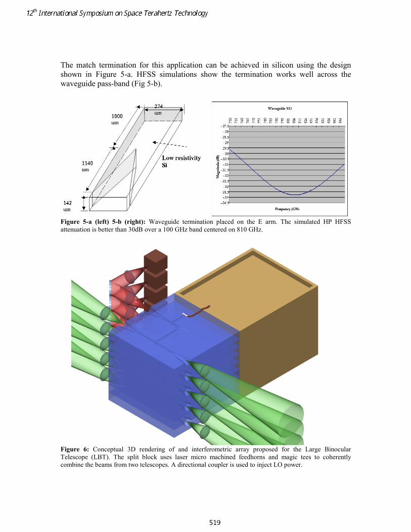
Figure 6: Conceptual 3D rendering of and interferometric array proposed for the Large Binocular Telescope (LBT). The split block uses laser micro machined feedhorns and magic tees to coherently combine the beams from two telescopes. A directional coupler is used to inject LO power.
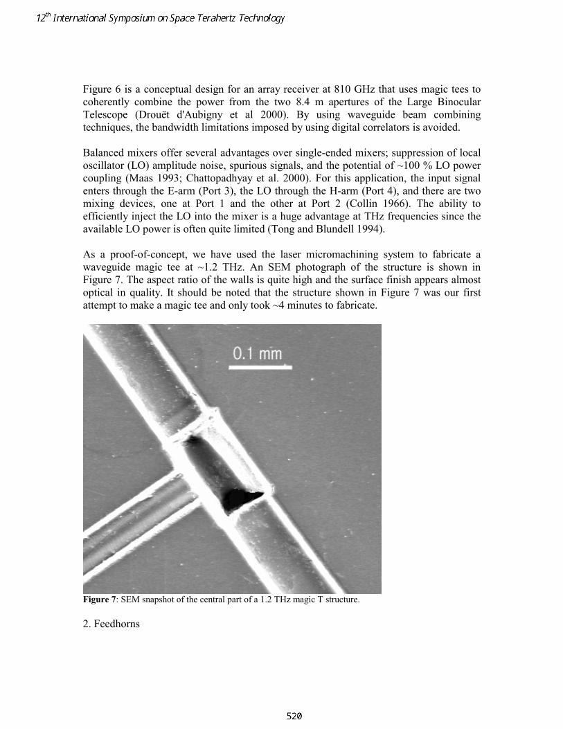
Figure 6 is a conceptual design for an array receiver at 810 GHz that uses magic tees to coherently combine the power from the two 8.4 m apertures of the Large Binocular Telescope (Drouët d'Aubigny et al 2000). By using waveguide beam combining techniques, the bandwidth limitations imposed by using digital correlators is avoided. Balanced mixers offer several advantages over single-ended mixers; suppression of local oscillator (LO) amplitude noise, spurious signals, and the potential of ~100 % LO power coupling (Maas 1993; Chattopadhyay et al. 2000). For this application, the input signal enters through the E-arm (Port 3), the LO through the H-arm (Port 4), and there are two mixing devices, one at Port 1 and the other at Port 2 (Collin 1966). The ability to efficiently inject the LO into the mixer is a huge advantage at THz frequencies since the available LO power is often quite limited (Tong and Blundell 1994). As a proof-of-concept, we have used the laser micromachining system to fabricate a waveguide magic tee at ~1.2 THz. An SEM photograph of the structure is shown in Figure 7. The aspect ratio of the walls is quite high and the surface finish appears almost optical in quality. It should be noted that the structure shown in Figure 7 was our first attempt to make a magic tee and only took ~4 minutes to fabricate.
Figure 7: SEM snapshot of the central part of a 1.2 THz magic T structure. 2. Feedhorns
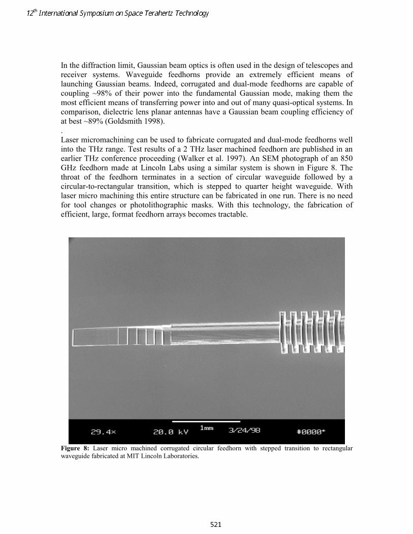
In the diffraction limit, Gaussian beam optics is often used in the design of telescopes and receiver systems. Waveguide feedhorns provide an extremely efficient means of launching Gaussian beams. Indeed, corrugated and dual-mode feedhorns are capable of coupling ~98% of their power into the fundamental Gaussian mode, making them the most efficient means of transferring power into and out of many quasi-optical systems. In comparison, dielectric lens planar antennas have a Gaussian beam coupling efficiency of at best ~89% (Goldsmith 1998). . Laser micromachining can be used to fabricate corrugated and dual-mode feedhorns well into the THz range. Test results of a 2 THz laser machined feedhorn are published in an earlier THz conference proceeding (Walker et al. 1997). An SEM photograph of an 850 GHz feedhorn made at Lincoln Labs using a similar system is shown in Figure 8. The throat of the feedhorn terminates in a section of circular waveguide followed by a circular-to-rectangular transition, which is stepped to quarter height waveguide. With laser micro machining this entire structure can be fabricated in one run. There is no need for tool changes or photolithographic masks. With this technology, the fabrication of efficient, large, format feedhorn arrays becomes tractable.
Figure 8: Laser micro machined corrugated circular feedhorn with stepped transition to rectangular waveguide fabricated at MIT Lincoln Laboratories.

Figure 9-a, below, is a conceptual drawing of a 10x10 array of laser machined, dual-mode feedhorns to be used in an 810 GHz prime focus camera for the LBT. The small (1.2 mm diameter) feedhorns are the only quasi-optical components needed. The geometry of a dual-mode feedhorn obviates the need of split-block construction. All 100 feedhorns can be machined in a single small (~1.5x1.5 cm) square of silicon. Metallization of the feedhorns will be performed using an e-beam evaporator. An HFSS simulation of the emergent beam pattern from one of the horns is shown in figure 6-b.
Figure 9-a (top), 9-b (bottom): 3D rendering of a 10x10 array of dual mode feedhorns for a prime focus camera to be used on the Large Binocular Telescope. a) Design of laser machined array. b) Predicted beam pattern from an individual horn made using HP HFSS: E-plane black line, H plane dashed line.

3. Anti-Reflection (AR) Coatings Dielectric lenses are widely used in sub-millimeter-wave systems. They play a critical role in forming the beam of planar antennas, such as the double slot and dipole. In addition, quasi-optical systems utilizing dielectric lenses are often more compact than comparable systems designed using reflective optics. The main disadvantages of using lenses are reflective losses off their surfaces and absorption of power in the lens material itself. With the proper choice of dielectrics, such as silicon, the absorption losses can often be kept to only a few percent. However, the reflected power off the surfaces of even low index of refraction materials (e.g. Teflon) can be as high as 12%. Lenses made with higher dielectric materials have shorter focal lengths and greater mechanical strength. To overcome the increase in the fractional power reflected from the surfaces of such materials, they must be coated with one or more layers of a dielectric with an index of refraction intermediate between the lens material and free space (Goldsmith 1998). Alternatively, the surface of the lens itself can be machined to simulate the required matching layer (Morita and Cohn 1955). In practice, this is usually achieved by etching concentric, λ/4 grooves in the dielectric surface. An example of a 1.5 THz AR grooved silicon window is shown in Figure 8-a. The bandwidth of the matching layer can be increased by etching grooves with a triangular cross-section several wavelengths deep. However, both the rectangular and triangular concentric grooves are polarization sensitive. This sensitivity can be avoided if an array of holes is used instead of concentric grooves to simulate the required dielectric layer. If the holes have a conical cross section and are several wavelengths deep, the surface can also be used over a wide frequency band (Lesurf 1990). A 3-D CAD representation of such a surface made in silicon for operation at 1.5 THz is shown in Figure 10-b. Due to their small size scales, it has been impossible to use simulated dielectrics as AR coatings at THz frequencies. However, with laser micro machining it is straightforward to machine either concentric grooves or holes like those depicted in Figure 8 directly into silicon quasi-optical components, such as lenses and vacuum windows. We plan to utilize these structures in THz receiver systems we are constructing for AST/RO and SOFIA.
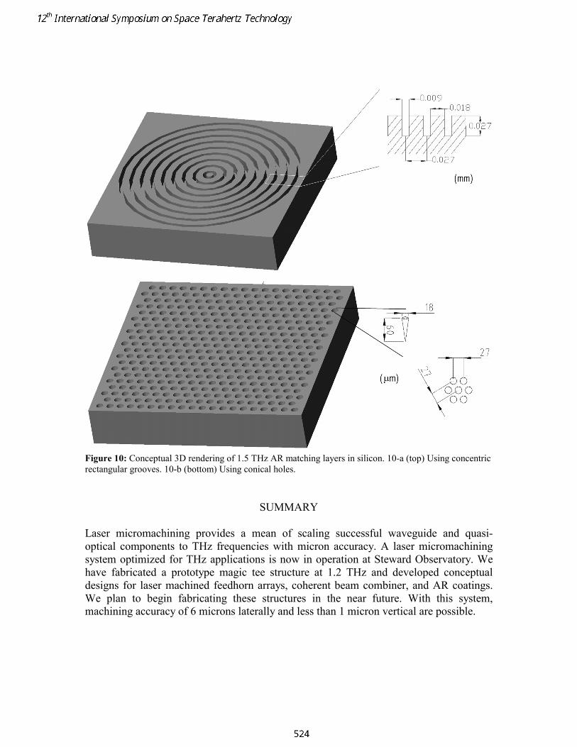
Figure 10: Conceptual 3D rendering of 1.5 THz AR matching layers in silicon. 10-a (top) Using concentric rectangular grooves. 10-b (bottom) Using conical holes.
SUMMARY Laser micromachining provides a mean of scaling successful waveguide and quasi-optical components to THz frequencies with micron accuracy. A laser micromachining system optimized for THz applications is now in operation at Steward Observatory. We have fabricated a prototype magic tee structure at 1.2 THz and developed conceptual designs for laser machined feedhorn arrays, coherent beam combiner, and AR coatings. We plan to begin fabricating these structures in the near future. With this system, machining accuracy of 6 microns laterally and less than 1 micron vertical are possible.
AKNOWLEDGEMENTS
This work was supported in part by NSF grant ECS 9800260 and NASA grant NAG5 9100. The authors also thank Kevin Righter and Kenneth Domanik of The Lunar and Planetary Laboratory for both optical and SEM pictures of the magic Tee.
REFERENCES
Bloomstein, T., Ph-D Thesis, MIT, 1996, Chattopadhyay, G., Rice, F., Miller, D., LeDuc, H., and Zimuidzinas, J., 2000, IEEE Microwave and Guides Wave Letters, in press. Collin, R., 1966, in ``Foundations of Microwave Engineering'', pub. McGraw Hill, p. 285. Drouët d'Aubigny, C., Walker, C., Groppi, C., Hill, J., Bieging, J, and Popmpea, S., 2000, Proc. SPIE, 4015, p. 268. Goldsmith, P., 1998, in ``Quasioptical Systems'', publ. IEEE Press, p. 184. LeSurf, J., 1990, in ``Millimeter-wave, Optics, Devices & Systems'', publ. Adam Hilger, p.22. Mass, S., 1986, in `` Microwave Mixers'', publ. Artech House Inc., p. 213. Morita, T. and Cohn, S., 1956, IRE Trans. on Antennas and Propagation, vol. AP-3, p.33. Rizzi, P., 1988, in ``Microwave Engineering (Passive Circuits)'', publ. Prentice Hall, p. 358 & 365. Tong, E. and Blundell, R., 1994, IEEE Trans. Microwave Theory and Techniques, vol. MTT-42, no. 3, p. 383. Walker, C., Narayanan G., Knoepfle, H., Capara, J., Glenn, J., Hungerford, A., Bloomstein, T., Palmacci, S., Stern, M., and Curtin, J., 1997, Proceedings of the Eighth International Symposium on Space TeraHertz Technology, eds. Blundell and Tong, Harvard University, p. 358.