laser reflectace iterferometry system with a 405 …ms_2013_543.pdf · m.kraszewski, r.bogdanowicz:...
TRANSCRIPT

Metrol. Meas. Syst., Vol. XX (2013), No. 4, pp. 543–554.
_____________________________________________________________________________________________________________________________________________________________________________________
Article history: received on Jan. 17, 2013; accepted on Sep. 06, 2013; available online on Dec. 10, 2013; DOI: 10.2478/mms-2013-0046.
METROLOGY A�D MEASUREME�T SYSTEMS
Index 330930, ISS� 0860-8229
www.metrology.pg.gda.pl
LASER REFLECTACE ITERFEROMETRY SYSTEM WITH A 405 M LASER
DIODE FOR I SITU MEASUREMETS OF CVD DIAMOD THICKESS
Maciej Kraszewski, Robert Bogdanowicz
Gdansk University of Technology, G.�arutowicza 11/12, 80-233 Gdansk, Poland (� [email protected], +48 792-064-003)
Abstract
In situ monitoring of the thickness of thin diamond films during technological processes is important because it
allows better control of deposition time and deeper understanding of deposition kinetics. One of the widely used
techniques is laser reflectance interferometry (LRI) which enables non-contact measurement during CVD
deposition. The authors have built a novel LRI system with a 405 nm laser diode which achieves better
resolution compared to the systems based on He-Ne lasers, as reported so far. The system was used for in situ
monitoring of thin, microcrystalline diamond films deposited on silicon substrate in PA-CVD processes.
The thickness of each film was measured by stylus profilometry and spectral reflectance analysis as a reference.
The system setup and interferometric signal processing are also presented for evaluating the system parameters,
i.e. measurement uncertainty, resolution and the range of measurable film thickness.
Keywords: interferometry, thin films, CVD, diamond, in situ measurements
© 2013 Polish Academy of Sciences. All rights reserved
1. Introduction
The thickness measurement in thin dielectric films manufactured by PA-CVD processes is
critical for the evaluation and optimization of a technological process [1-3]. It allows
determining the film growth rate and deposition of films with a specified thickness. Among
numerous thickness measurement methods, the most often used ones are (I) stylus
profilometry [4], (II) scanning electron microscopy (SEM) [5] and (III) optical methods
(ellipsometry, time- and spectral-domain interferometry) [6-13].
The optical methods are generally characterized by an indirect way of measurement. Film
thickness is being determined based on parameters of light transmitted or reflected from the
film surface: (I) polarisation (ellipsometry) [8], (II) intensity (time-domain interferometry)
[10-13] or (III) spectrum (spectral-domain interferometry) [9,13]. Optical techniques are
based on the assumed film optical model therefore the model parameters inaccuracy can cause
errors in the thickness measurement. This is the main drawback of the optical methods
compared to the direct measurements by stylus profilometry or SEM [9].
However, the optical methods allow performing a no-contact and non-destructive
measurement. Moreover, they enable in situ film monitoring which is critical in diagnostics or
studying of CVD process kinetics [6,14]. In optical systems, the angle of incidence of light
onto the film may be fixed [10-12] or scanned within a specified range [15-17]. The second
approach allows an analysis of additional features of the film, such as surface quality [15] or
mechanical stress [16], however they are difficult to apply for in situ measurement, where the
light angle of incidence is defined by the construction of the CVD reactor chamber.
Laser reflectance interferometry (LRI) is an in situ monitoring technique for growing
diamond films in CVD processes [10-12]. It involves the measurement of the intensity
of laser light reflected from the film during its growth. Several LRI systems based on He-Ne
lasers have been reported [10-12]. Film thickness can be calculated by fitting the parameters

M.Kraszewski, R.Bogdanowicz: LASER REFLECTA�CE I�TERFEROMETRY SYSTEM USI�G 405 �M LASER DIODE …
of the assumed film optical model (thickness, refractive index and surface roughness) to the
measured interferometric signal [10] or by counting the extremes of film reflectance [12].
The extremes counting methods allow to perform the thickness measurement with
a resolution equal to a quarter of wavelength of the light in the investigated film [12]. He-Ne
lasers with a wavelength of 632.8 nm provides the measurement resolution of 65.6 nm (with
refractive index of diamond equal to 2.41 [12]). The aforementioned value is valid assuming
normal incidence of laser light on the measured sample; it decreases with decreasing angle
of incidence.
Currently, the progress in laser diodes technology makes it possible to build inexpensive
LRI systems based on light sources with light wavelengths shorter than those in He-Ne lasers.
This enables achieving a better measurement resolution. The authors have built a novel LRI
system with a 405 nm laser diode. In this system, the layer thickness is calculated from the
number of extremes in the intensity of light reflected from the growing diamond film.
The system setup, applied algorithms of the digital signal processing and evaluation of system
metrological parameters are presented below.
2. Measurement principles
2.1. Measurement setup
The 405 nm LRI home-made setup is presented in Fig. 1. It consists of a 405 nm laser
diode (L) with 100 mW output power. Laser radiation is transmitted onto the sample (S)
inside the CVD reactor chamber via a quartz viewport at the angle of incidence of 45°.
The light reflected from the diamond film is transmitted via a second viewport to a silicon
photodiode (D). The generated photo-current is transformed to a voltage signal by
a transconductance amplifier (W), converted to digital form by an analog-to-digital converter
(A) and sent to a PC.
Fig. 1. 405 nm LRI system for measuring the growth of thin diamond films.
2.2. Interference in thin dielectric films
The reflectance of a thin dielectric film, deposited on a specified substrate, can be
calculated according to the following formula:
( )
( )βdcos2
R1
R2+2
R1
R+1
βdcos2
R1
R2+2
R+1
R=R , (1)
where R is the reflectance of the film; R1 and R2 are reflection coefficients at the ambient-film
and film-substrate boundary, respectively; d is the thin film thickness; and β is given by (2):
11
cos4π
φnλ
=β , (2)
Metrol. Meas. Syst., Vol. XX (2013), No. 4, pp. 543–554.
where λ is the wavelength of light; n1 is the refractive index of the film and φ1 is the angle
of refraction of light inside the film.
Assuming a 405 nm light source, 45° angle of light incidence and the refractive index
of diamond equal to 2.46 (value for natural diamond at a wavelength of 405 nm), the value
of β for the designed system can be calculated from (3):
0.0732 1β = nm− . (3)
During the film growth, as the film thickness increases, the signal detected by the photodiode
achieves its extremes for:
mπ=βd , (4)
for ...0,1,2,=m . (5)
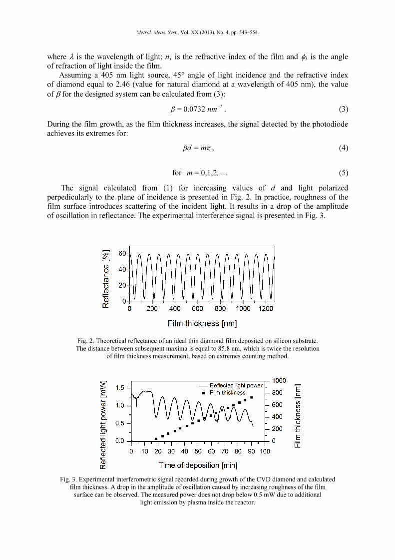
The signal calculated from (1) for increasing values of d and light polarized
perpedicularly to the plane of incidence is presented in Fig. 2. In practice, roughness of the
film surface introduces scattering of the incident light. It results in a drop of the amplitude
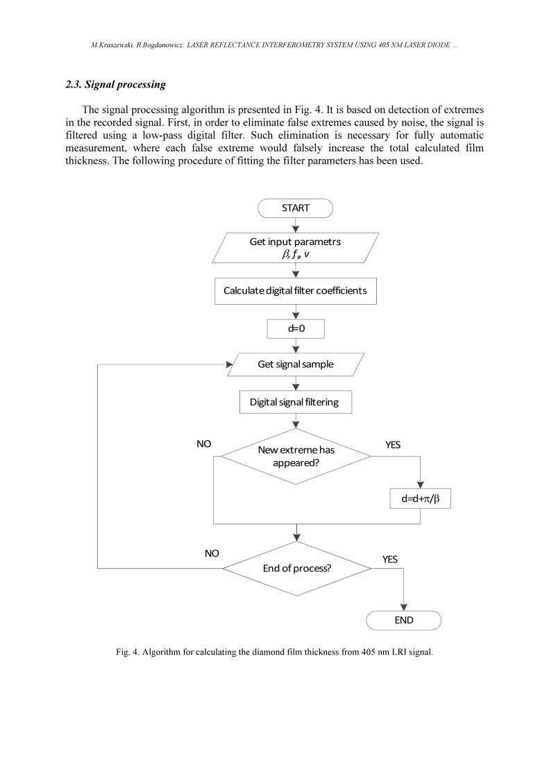
of oscillation in reflectance. The experimental interference signal is presented in Fig. 3.
Fig. 2. Theoretical reflectance of an ideal thin diamond film deposited on silicon substrate.
The distance between subsequent maxima is equal to 85.8 nm, which is twice the resolution
of film thickness measurement, based on extremes counting method.
Fig. 3. Experimental interferometric signal recorded during growth of the CVD diamond and calculated
film thickness. A drop in the amplitude of oscillation caused by increasing roughness of the film
surface can be observed. The measured power does not drop below 0.5 mW due to additional
light emission by plasma inside the reactor.
M.Kraszewski, R.Bogdanowicz: LASER REFLECTA�CE I�TERFEROMETRY SYSTEM USI�G 405 �M LASER DIODE …
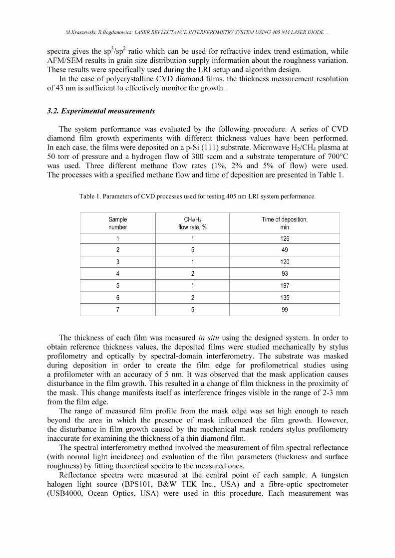
2.3. Signal processing
The signal processing algorithm is presented in Fig. 4. It is based on detection of extremes
in the recorded signal. First, in order to eliminate false extremes caused by noise, the signal is
filtered using a low-pass digital filter. Such elimination is necessary for fully automatic
measurement, where each false extreme would falsely increase the total calculated film
thickness. The following procedure of fitting the filter parameters has been used.
Fig. 4. Algorithm for calculating the diamond film thickness from 405 nm LRI signal.
START
Get input parametrs:β, f
s, v
Get signal sample
New extreme has
appeared?
d=d+π/β
d=0
Digital signal filtering
Calculate digital filter coefficients
End of process?
YES
YES
NO
NO
END

Metrol. Meas. Syst., Vol. XX (2013), No. 4, pp. 543–554.
The predicted, normalized frequency of oscillation is calculated based on the knowledge
of β, the signal sampling frequency (fs) and a rough estimate of the film growth rate (v),
as (6):
ssf
βv=
f
f. (6)
The IIR Butterworth filter coefficients are calculated using the bilinear transformation
method with cut-off frequency equal to 1.5 of the normalized frequency calculated using (6).
The thickness of the film is calculated based on the number of extremes in the filtered
signal, according to (7):
β
πm=d , (7)
where m is the number of recorded extremes.
3. Analysis of system performance
3.1. Theoretical analysis
According to (1) and (2), the following effects can influence the 405 nm LRI system error:
• a shift in the refractive index of the film by δn [18]
• a quantization error arising from the fact that the number of extremes can only assume
positive integer values
• inhomogeneous film growth with varying film thickness for different spots on the
film, marked as δd.
Assuming the lack of correlation between the above listed effects, the total relative
measurement uncertainty can be estimated as:
222
m
δm+
d
δd+
n
δn=ε . (8)
Measurement resolution is equal to film growth corresponding to two neighboring
extremes in the interference signal. Its value can be calculated based on (3) and (4).
The least detectable difference ∆d of film thickness is given as (9):
nm=β
π=∆d 42.9 . (9)
Only the δm value in (8) can be calculated analytically; it can reach a maximal value of 1.
To achieve a relative quantization error less than 10%, more than 10 reflectance extremes
need to be recorded. This requires that the grown diamond films are at least 429 nm thick.
The values of δn and δd can be estimated by ex situ examination of diamond films with
spectral interferometry.
Higher measurement resolution could be obtained by advanced interference signal
processing algorithms. Such methods are efficient for flat surfaces deposited with atomic
precision. CVD diamond films exhibit significant surface roughness that introduces light
scattering and deterioration of the interference signal. This makes advanced interference
signal processing difficult to apply.
The trends in roughness and refractive index were taken from our previous studies based
on Raman spectroscopy and AFM/SEM measurements [19, 20]. Deconvolution of Raman
M.Kraszewski, R.Bogdanowicz: LASER REFLECTA�CE I�TERFEROMETRY SYSTEM USI�G 405 �M LASER DIODE …
spectra gives the sp3/sp
2 ratio which can be used for refractive index trend estimation, while
AFM/SEM results in grain size distribution supply information about the roughness variation.
These results were specifically used during the LRI setup and algorithm design.
In the case of polycrystalline CVD diamond films, the thickness measurement resolution
of 43 nm is sufficient to effectively monitor the growth.
3.2. Experimental measurements
The system performance was evaluated by the following procedure. A series of CVD
diamond film growth experiments with different thickness values have been performed.
In each case, the films were deposited on a p-Si (111) substrate. Microwave H2/CH4 plasma at
50 torr of pressure and a hydrogen flow of 300 sccm and a substrate temperature of 700°C
was used. Three different methane flow rates (1%, 2% and 5% of flow) were used.
The processes with a specified methane flow and time of deposition are presented in Table 1.
Table 1. Parameters of CVD processes used for testing 405 nm LRI system performance.
Sample number
CH4/H2 flow rate, %
Time of deposition, min
1 1 126
2 5 49
3 1 120
4 2 93
5 1 197
6 2 135
7 5 99
The thickness of each film was measured in situ using the designed system. In order to
obtain reference thickness values, the deposited films were studied mechanically by stylus
profilometry and optically by spectral-domain interferometry. The substrate was masked
during deposition in order to create the film edge for profilometrical studies using
a profilometer with an accuracy of 5 nm. It was observed that the mask application causes
disturbance in the film growth. This resulted in a change of film thickness in the proximity of
the mask. This change manifests itself as interference fringes visible in the range of 2-3 mm
from the film edge.
The range of measured film profile from the mask edge was set high enough to reach
beyond the area in which the presence of mask influenced the film growth. However,
the disturbance in film growth caused by the mechanical mask renders stylus profilometry
inaccurate for examining the thickness of a thin diamond film.
The spectral interferometry method involved the measurement of film spectral reflectance
(with normal light incidence) and evaluation of the film parameters (thickness and surface
roughness) by fitting theoretical spectra to the measured ones.
Reflectance spectra were measured at the central point of each sample. A tungsten
halogen light source (BPS101, B&W TEK Inc., USA) and a fibre-optic spectrometer
(USB4000, Ocean Optics, USA) were used in this procedure. Each measurement was

Metrol. Meas. Syst., Vol. XX (2013), No. 4, pp. 543–554.
preceded by recording the spectrum of light reflected from bulk, monocrystalline Si (111)
with a known reflectance spectrum for the wavelength range of 400-900 nm.
Theoretical spectra were calculated using the theory of light reflection from rough
surfaces [21-22].
Variations in the reflectance spectrum of films with an optical thickness shift of 1 nm can
be easily detected. However, deviations of the refractive index limit the accuracy of the
spectral interferometry method. As described in section 3.2., refractive index fluctuations
of 5% should be expected. Using optimization methods, such as the Levenberg-Marquadt
algorithm [23] allows finding an approximated value of the film refractive index from the
reflectance spectra.
In situ measurements and the reference thickness values obtained by both aforementioned
methods are presented in Table 2, and graphically in Fig. 5. For all optical measurements,
the film refractive index and dispersion have been assumed to be equal to those of natural
diamond. Relative errors of LRI measurement, compared to each reference method has been
presented as well.
Relative differences between results of profilometry and LRI vary strongly for different
samples, but smaller errors have been generally obtained for thicker films. It suggests that
they are mostly caused by quantization error, as described further. Differences between LRI
and spectral reflectance measurement methods take the same sign for all samples and very
similar values for all of them. This suggests the presence of systematic error in one of the
methods.
Table 2. Comparison of the film thickness measurements by LRI and reference methods.
Sample number
Thickness measured by LRI [nm]
Thickness measured by profilometry [nm]
Relative error of LRI
Thickness measured by fitting spectral reflectance [nm]
Relative error of LRI
1 515.0 423.4 22% 542 -5%
2 557.9 552.3 1% 638 -13%
3 557.9 780.1 -28% 659 -15%
4 729.6 607.6 20% 823 -11%
5 1030.0 1043.9 -1% 1164 -12%
6 1115.9 1125.5 -1% 1266 -12%
7 1416.3 1197.3 18% 1613 -12%

M.Kraszewski, R.Bogdanowicz: LASER REFLECTA�CE I�TERFEROMETRY SYSTEM USI�G 405 �M LASER DIODE …
Fig. 5. Comparison of film thickness measured by using the 405 nm LRI system and reference methods.
The results in Fig. 5 and Table 2 show that the differences between in situ determination
and the reference methods can exceed the calculated uncertainty. This finding concerns
samples 1 and 3 for profilometry, and sample 3 for the spectral reflectance analysis.
Differences between LRI and profilometry results vary in character. Samples 2, 5 and 6
show very good agreement between the two methods since other LRI results assume smaller
or larger values compared with profilometry data. LRI measurement requires an assumption
of the film refractive index value. If its real value differs from the assumed one, erroneous
results are obtained. On the other hand, masking a part of the substrate in order to prepare
a sample for profilometric examination disturbs the film growth. These two phenomena are
likely to be the main causes of the observed differences.
For every film, the thickness values measured by spectral reflectance analysis are about
10% greater than those obtained by LRI. This suggests a systematic phenomenon influencing
the results. One possible explanation is the position of the substrate during the CVD
processes. The laser beam used for in-situ measurement usually does not hit the exact centre
of the growing film where the growth rate is expected to achieve its highest values.
3.3. Estimation of measurement uncertainty
The Cauchy model of material dispersion has been assumed for estimating the shift in
refractive index of the films:
4
4
2
2
λ
�+
λ
�+n=n
0, (10)
4
4
2
2
λ
K+
λ
K+k=k
0, (11)
where n and k are real and imaginary parts of the complex refractive index. Examination
of thin diamond films by spectroscopic ellipsometry shows that the Cauchy model can be
successfully applied to film refractive index in the visible light range [24].
Model parameters n0, �2, �4, k0, K2 and K4 from (10) and (11) have been calculated by
fitting theoretical reflectance spectra to the measured ones using the Levenberg-Marquadt
Algorithm (LMA). LMA is an optimization algorithm which fits parameters of the theoretical
model to the measured values in order to minimize the square mean error of the fitted function
[23].
Metrol. Meas. Syst., Vol. XX (2013), No. 4, pp. 543–554.
A successful application of LMA requires that the chosen initial values of the model
parameters are close to the final ones. For initial values that are too far from the solution,
the algorithm may find only a local minimum of the error.
To calculate the reflectance spectra, initial values of thickness and surface roughness
(defined as standard deviation of the film thickness) are required. Efficient results of LMA
calculation have been obtained using the initial value of film thickness measured by the LRI
system (Table 2). The initial value of surface roughness was kept at 0. The natural diamond
refractive index was chosen for initial Cauchy model purposes.
The calculated values of n for a wavelength of 405 nm are presented in Table 3.
Table 3. Refractive indices of deposited films calculated by fitting spectral reflectance method.
Sample number
Film refractive index
1 2.39
2 2.46
3 2.55
4 2.36
5 2.43
6 2.41
7 2.57
The mean value of the obtained refractive indices is equal to:
2.45,n = (12)
which is close to the assumed value for natural diamond. The standard deviation of the results
and its value relative to the mean are equal to, respectively:
0.080=σn
, (13)
3.3%=
n
σn . (14)
To obtain the value of uncertainty of film thickness due to inhomogeneous film growth
(∆d from (8)), the thickness of each sample was measured using spectral-domain
interferometry at seven different points on the film surface. For each film, the standard
deviation of thickness relative to the mean was calculated. The mean relative standard
deviation from all films was equal to:
5.0%=d
σd . (15)
Assuming that n
=∆n 3σ and d
=∆d 3σ , the values of relative measurement uncertainty
from (8) for different thicknesses of the film were plotted in Fig. 6. It was noted that for films
thicker than 500 nm, the quantization error becomes insignificant compared to the uncertainty
of refractive index and the effect of inhomogeneous film growth. This finding justifies the use
of the simple extremes counting method as an efficient way to calculate film thickness from
the interferometric signal. For films with thickness values above 500 nm, the uncertainty

M.Kraszewski, R.Bogdanowicz: LASER REFLECTA�CE I�TERFEROMETRY SYSTEM USI�G 405 �M LASER DIODE …
reaches values smaller than 20%. Results in Fig. 6 may explain larger differences between
LRI and profilometry measurements for a film with smaller thickness, as shown in Tab. 2.
Fig. 6. Relationship between the measurement uncertainty and the layer thickness.
A decreasing influence of quantization error on the entire uncertainty value can be observed.
3.4. Influence of film surface roughness
The uneven growth of polycrystalline diamond film causes an increase of film surface
roughness during CVD. Rough surface introduces the loss of coherence of the reflected light
wave and increases the diffuse part of the reflectance [19]. This effect manifests itself
as a drop in oscillation amplitude and the mean value in the interference signal, as presented
in Fig. 3. A decrease of oscillation amplitude below the detection level makes further
thickness measurements impossible. The maximal sample thickness possible to be measured
depends on particular parameters of the process. For the performed test processes listed
in Table 1, the upper limit of thickness measurement was estimated at 2 µm.
4. Conclusions
A novel 405 nm LRI system for in situ diagnostics of thin film growth has been
developed. The performance of the system was studied by analyzing seven CVD diamond
film samples deposited on silicon substrates. The film thickness and refractive index were
examined in samples using stylus profilometry and spectral reflectance analysis.
For LRI measurements, film thickness was calculated by counting extremes in an
interferometric signal. This method introduces a quantization error to the results.
For sufficently thick films, the value of this error is insignificant compared to the uncertainty
of the film refractive index and the effect of uneven diamond growth. The relative uncertainty
of the thickness measurement was estimated to be better than 20% which is valid for a film
thicker than 500 nm.
Measurement resolution for the extremes counting method was 43 nm. The upper limit of
measurable film thickness is determined by the film surface roughness, which causes a drop
in oscillations in the interferometric signal. The limit value was experimentally determined to
be 2 µm. In specific cases, the limit value depends on the parameters of the CVD process
which determines the film surface roughness.

Metrol. Meas. Syst., Vol. XX (2013), No. 4, pp. 543–554.
Acknowledgements
This work was supported by the Polish National Science Center (NCN) under the Grant
No. 2011/03/D/ST7/03541 and by the National Center for Research and Development
(NCBiR) under project No. LIDER/20/91/L-2/10. The DS funds of the Faculty of Electronics,
Telecommunications and Informatics of the Gdansk University of Technology are also
acknowledged.
References
[1] Bogdanowicz, R., Gnyba, M., Wroczynski, P., Kosmowski, B.B. (2010). Optoelectronic system for
monitoring of thin diamond layers growth. Journal of Optoelectronics and Advanced Materials, 12,
1660−1665.
[2] Smietana, M., Szmidt, J., Korwin-Pawlowski, M.L., Bock, W., Grabarczyk, J. (2007). Application of
diamond-like carbon films in optical fibre sensors based on long-period gratings. Diamond and Related
Materials, 16, 1374−1377.
[3] Smietana, M., Szmidt, J., Dudek, M., Niedzielski, P. (2004). Optical properties of diamond-like cladding
for optical fibres. Diamond and Related Materials, 13, 954−957.
[4] Spanos, C.J., May, G.S. (2006). Fundamentals of Semiconductor Manufacturing and Process Control. John
Wiley & Sons, Ltd.
[5] Wang, Z.L., Zhou, W. (2006). Scanning Microscopy of !anotechnology – Techniques and Applications.
Springer-Verlag.
[6] Bogdanowicz, R., Gnyba, M., Wroczynski, P. (2006). Optoelectronic monitoring of plasma discharge
optimized for thin diamond film synthesis. Journal de Physique IV (Proceedings), 137, 57−60.
[7] Bogdanowicz, R., Ryl, J. (2007). Ellipsometric data analysis used in on-line metal passivation monitoring.
Eur. Phys. J. Spec. Top, 144, 215−220.
[8] Irene, E.A., Tompkins, H.G. (2005). Handbook of Ellipsometry. William Andrew Publishing/Springer.
[9] Jennet, H., Bubert, H. (2002). Surface and Thin Film Analysis. John Wiley & Sons, Ltd.
[10] Luo, J., Ying, X., Wang, P., Chen, L. (2002). Study of the growth of CVD diamond thin films by in situ
reflectivity measurement. Diamond and Related Materials, 11, 1871−1875.
[11] Bonnot, A.M., Schauer, R., Weidner, B. (1998). HFCVD diamond film nucleation and growth studies by in
situ optical technique and ex-situ AFM observations. Diamond and Related Materials., 7, 205−208.
[12] Zuiker, C.D., Gruen, D.M., Krauss, A.R. (1996). In situ reflectance interferometry measurement of
diamond film growth. Journal of Applied Physics, 79, 3541−3547.
[13] Plucinski, J., Hypszer, R., Wierzba, P., Strakowski, M., Jedrzejewska-Szczerska, M., Maciejewski, M.,
Kosmowski, B.B. (2008). Optical low-coherence interferometry for selected technical applications.
Bulletin of the Polish Academy of Sciences, Technical Sciences, 56(2), 155−172.
[14] Fabianska, A., Ossowski, T., Bogdanowicz, R., Czupryniak, J., Gnyba, M., Odzga, T., Janssens, S.D.,
Haenen, K., Siedlecka, E.M. (2012). Electrochemical oxidation of ionic liquids at highly boron doped
diamond electrodes. Physica Status Solidi (a), 209, 1797−1803.
[15] Wolter, S.D., Schlesser, R., Okuzumi, F., Prater, J.T., Sitar, Z. (2001). Angle-dependent reflectometry
as a technique for fast assessment of highly oriented diamond film quality. Diamond and Related
Materials., 10(11), 2092−2095.
[16] Paszek, M.J., DuFort, C.C., Rubashkin, M.G., Davidson, M.W., Thorn, K.S., Liphardt, J.T., Weaver, V.M.
(2012). Scanning angle interference microscopy reveals cell dynamics at the nanoscale. !ature Methods.,
9, 825−827.
[17] Sethuraman, V.A., Chon, M.J., Shimshak, M., Srinivasan, V,. Guduru, P.R. (2010). In situ measurements
of stress evolution in silicon thin films during electrochemical lithiation and delithiation. Journal
of Power Sources., 195(15), 5062−5066.
M.Kraszewski, R.Bogdanowicz: LASER REFLECTA�CE I�TERFEROMETRY SYSTEM USI�G 405 �M LASER DIODE …
[18] Vogel, M., Stenzel, O., Petrich, R., Schaarschmidt, G., Scharff, W. (1993). The position of the
fundamental absorption edge and activation energies for thermally activated electrical conductivity in
amorphous carbon layers. Thin Solid Films, 227, 74−89.
[19] Fabiańska, Ossowski, T., Bogdanowicz, R., Czupryniak, J., Gnyba, J., Odzga, T., Janssens, S.D.,
Haenen, K., Siedlecka, E.M. (2012). Physica Status Solidi (a). 209, 1797−1803.
[20] Bogdanowicz, R., Czupryniak, J., Gnyba, M., Ryl, J., Ossowski, T., Sobaszek, M., Siedlecka, E.M.,
Darowicki, K. (2013). Sensors and Actuators B: Chemical .10.1016/j.snb.2012.12.007.
[21] Siapkas, D.I., Mitsas, C.L. (1995). Generalized matrix method for analysis of coherent and incoherent
reflectance and transmittance of multilayer structures with rough surfaces, interfaces and finite substrates.
Applied Optics, 34, 1678−1683.
[22] Katsidis, C., Siapkas, D.I. (2002). General transfer-matrix method for optical multilayer systems with
coherent, partially coherent and incoherent interference. Applied Optics, 41, 3978−3987
[23] Press, W.H., Teukolsky, S.A., Vetterling, W.T., Flannery, B.P. (1992). !umerical Recipes in C. Cambridge
University Press.
[24] Hu, Z.G., Prunici, P., Hess, P., Chen, K.H. (2007). Optical properties of nanocrystalline diamond films
from mid-infrared to ultraviolet using reflectometry and ellipsometry. Journal of Materials Science:
Materials in Electronics, 18, 37−41.