lc 75834
TRANSCRIPT
OverviewThe LC75834E, LC75834W, and LC75834JE are 1/4 dutygeneral-purpose LCD drivers that can be used forfrequency display in electronic tuners under the control ofa microcontroller. The LC75834E and LC75834W candrive an LCD with up to 136 segments directly, theLC75834JE can drive an LCD with up to 120 segmentsdirectly. The LC75834E and LC75834W and LC75834JEcan also control up to 8 general-purpose output ports.Since the LC75834E, LC75834W, and LC75834JE useseparate power supply systems for the LCD drive blockand the logic block, the LCD driver block power-supplyvoltage can be set to any voltage in the range 2.7 to 6.0volts, regardless of the logic block power-supply voltage.
Features• Supports both 1/4 duty 1/2 bias and 1/4 duty 1/3 bias
LCD drive under serial data control.LC75834E, LC75834W: up to 136 segmentsLC75834JE: up to 120 segments(without the S9, S18, S27, S34 segment output pinsfrom the LC75834E, LC75834W)
• Serial data input supports CCB format communicationwith the system controller.
• Serial data control of the power-saving mode basedbackup function and all the segments forced off function
• Serial data control of switching between the segmentoutput port and the general-purpose output portfunctions
• High generality, since display data is displayed directlywithout decoder intervention.
• Independent VLCD for the LCD driver block (VLCD canbe set to any voltage in the range 2.7 to 6.0 volts,regardless of the logic block power-supply voltage.)
• The INH pin can force the display to the off state.• RC oscillator circuit
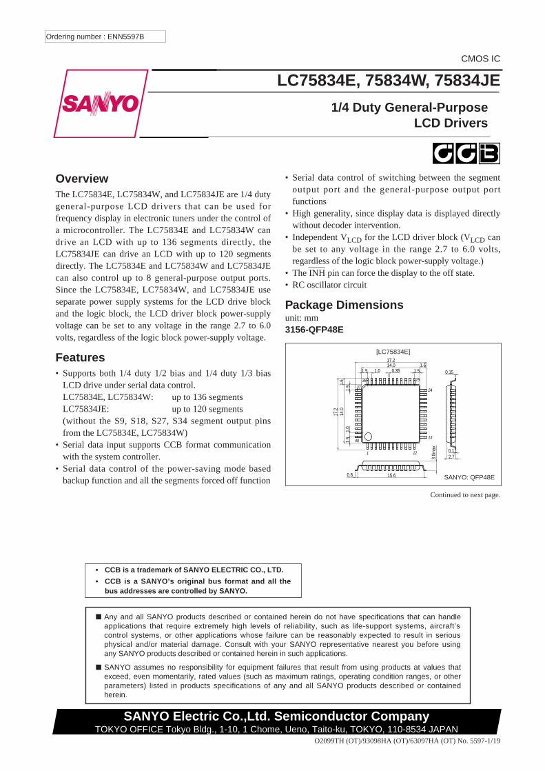
Package Dimensionsunit: mm3156-QFP48E
14.017.2
1.5 1.5 1.6
0.150.35
0.1
15.60.8
1.0
3.0m
ax
1
48
12
13
24
2536
37
2.7
14.0
17.2
1.5
1.5 1.
61.
0
• CCB is a trademark of SANYO ELECTRIC CO., LTD.
• CCB is a SANYO’s original bus format and all thebus addresses are controlled by SANYO.
[LC75834E]
SANYO: QFP48E
Ordering number : ENN5597B
O2099TH (OT)/93098HA (OT)/63097HA (OT) No. 5597-1/19
1/4 Duty General-Purpose LCD Drivers
LC75834E, 75834W, 75834JE
SANYO Electric Co.,Ltd. Semiconductor CompanyTOKYO OFFICE Tokyo Bldg., 1-10, 1 Chome, Ueno, Taito-ku, TOKYO, 110-8534 JAPAN
CMOS IC
Any and all SANYO products described or contained herein do not have specifications that can handleapplications that require extremely high levels of reliability, such as life-support systems, aircraft’scontrol systems, or other applications whose failure can be reasonably expected to result in seriousphysical and/or material damage. Consult with your SANYO representative nearest you before usingany SANYO products described or contained herein in such applications.
SANYO assumes no responsibility for equipment failures that result from using products at values thatexceed, even momentarily, rated values (such as maximum ratings, operating condition ranges, or otherparameters) listed in products specifications of any and all SANYO products described or containedherein.
Continued to next page.
SpecificationsAbsolute Maximum Ratings at Ta = 25°C, VSS = 0 V
Note: The LC75834JE do not have the S9, S18, S27 S34 output pins.
Allowable Operating Ranges at Ta = –40 to +85°C, VSS = 0 V
No. 5597-2/19
LC75834E, 75834W, 75834JE
Parameter Symbol Conditions Ratings Unit
Maximum supply voltageVDD max VDD –0.3 to +7.0 V
VLCD max VLCD –0.3 to +7.0 V
VIN 1 CE, CL, DI, INH –0.3 to +7.0 V
Input voltage VIN 2 OSC –0.3 to VDD + 0.3 V
VIN 3 VLCD 1, VLCD 2 –0.3 to VLCD + 0.3 V
Output voltageVOUT 1 OSC –0.3 to VDD + 0.3 V
VOUT 2 S1 to S34, COM1 to COM4, P1 to P8 –0.3 to VLCD + 0.3 V
IOUT 1 S1 to S34 300 µA
Output current IOUT 2 COM1 to COM4 3 mA
IOUT 3 P1 to P8 5 mA
Allowable power dissipation Pd max Ta = 85°C 150 mW
Operating temperature Topr –40 to +85 °C
Storage temperature Tstg –55 to +125 °C
Parameter Symbol ConditionsRatings
Unitmin typ max
Supply voltageVDD VDD 2.7 6.0 V
VLCD VLCD 2.7 6.0 V
Input voltageVLCD1 VLCD1 2/3 VLCD VLCD V
VLCD2 VLCD2 1/3 VLCD VLCD V
Input high level voltage VIH CE, CL, DI, INH 0.8 VDD 6.0 V
Input low level voltage VIL CE, CL, DI, INH 0 0.2 VDD V
Recommended external resistance ROSC OSC 43 kΩ
Recommended external capacitance COSC OSC 680 pF
Guaranteed oscillation range fOSC OSC 25 50 100 kHz
Data setup time tds CL, DI: Figure 2 160 ns
Data hold time tdh CL, DI: Figure 2 160 ns
CE wait time tcp CE, CL: Figure 2 160 ns
CE setup time tcs CE, CL: Figure 2 160 ns
CE hold time tch CE, CL: Figure 2 160 ns
High level clock pulse width tøH CL: Figure 2 160 ns
Low level clock pulse width tøL CL: Figure 2 160 ns
Rise time tr CE, CL, DI: Figure 2 160 ns
Fall time tf CE, CL, DI: Figure 2 160 ns
INH switching time tc INH, CE: Figure 3 10 µs
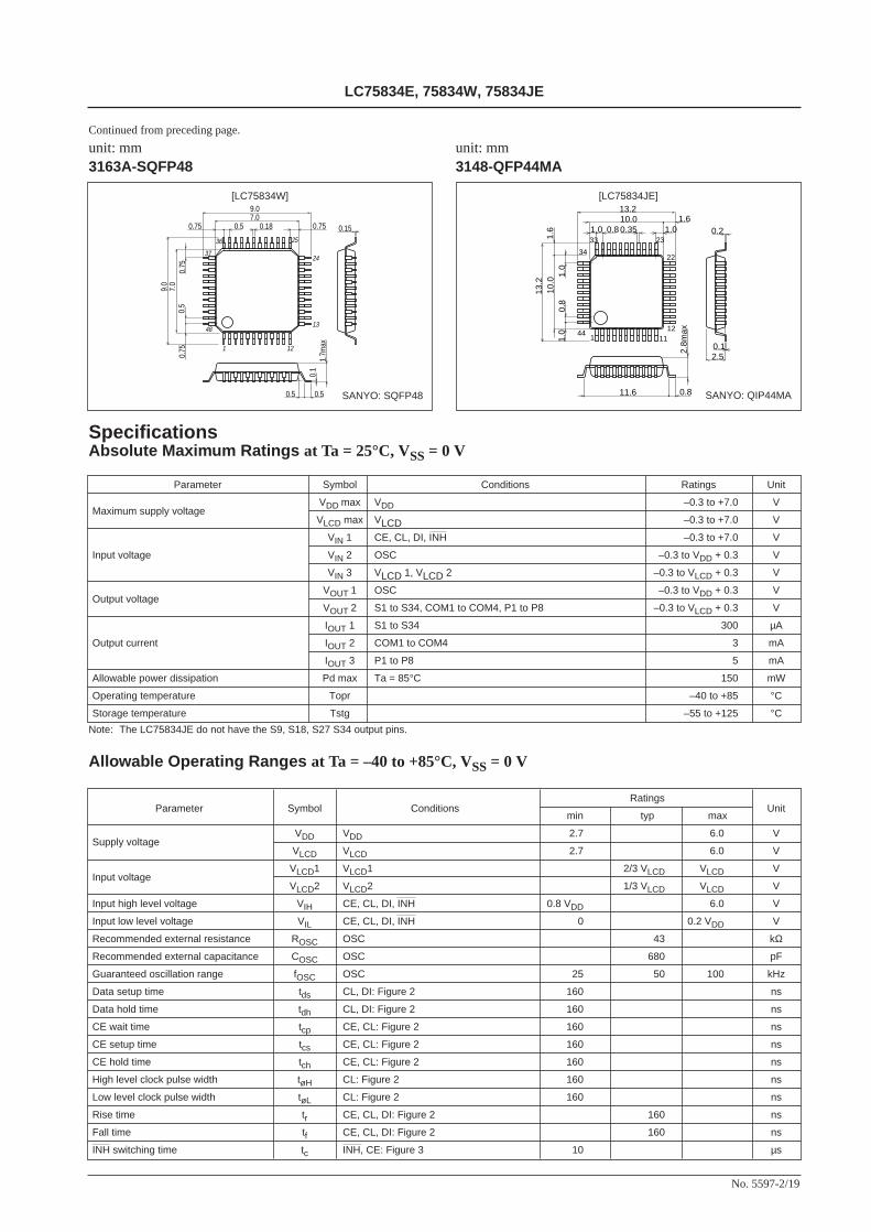
unit: mm3163A-SQFP48
unit: mm3148-QFP44MA
2.8m
ax
0.811.6
0.3510.013.2
1.0
1 1112
22
2333
34
44
1.01.6
0.8
2.5
0.2
0.1
10.0
13.2
1.0
1.0
1.6
0.8
[LC75834JE]
SANYO: QIP44MA0.5
7.0
9.0
0.150.180.75 0.5 0.75
0.75
0.5
0.75
0.5
0.1
1 12
13
24
2536
37
48
7.09.0
1.7m
ax
[LC75834W]
SANYO: SQFP48
Continued from preceding page.
No. 5597-3/19
LC75834E, 75834W, 75834JE
Electrical Characteristics for the Allowable Operating Ranges
Note: *1 Excluding the bias voltage generation divider resistors built in the VLCD1 and VLCD2. (See Figure 1.)
The LC75834JE do not have the S9, S18, S27, S34 output pins.
Parameter Symbol ConditionsRatings
Unitmin typ max
Hysteresis VH CE, CL, DI, INH 0.1 VDD V
Input high level current IIH CE, CL, DI, INH; VI = 6.0 V 5.0 µA
Input low level current IIL CE, CL, DI, INH; VI = 0 V –5.0 µA
VOH 1 S1 to S34; IO = –20 µA VLCD – 0.9 V
Output high level voltage VOH 2 COM1 to COM4; IO = –100 µA VLCD – 0.9 V
VOH 3 P1 to P8; IO = –1 mA VLCD – 0.9 V
VOL 1 S1 to S34; IO = 20 µA 0.9 V
Output low level voltage VOL 2 COM1 to COM4; IO = 100 µA 0.9 V
VOL 3 P1 to P8; IO = 1 mA 0.9 V
VMID 1 COM1 to COM4; 1/2 bias, 1/2 VLCD – 0.9 1/2 VLCD + 0.9 VIO = ±100 µA
VMID 2 S1 to S34; 1/3 bias, 2/3 VLCD – 0.9 2/3 VLCD + 0.9 VIO = ±20 µA
Output middle level voltage*1 VMID 3 S1 to S34; 1/3 bias, 1/3 VLCD – 0.9 1/3 VLCD + 0.9 VIO = ±20 µA
VMID 4 COM1 to COM4; 1/3 bias, 2/3 VLCD – 0.9 2/3 VLCD + 0.9 VIO = ±100 µA
VMID 5 COM1 to COM4; 1/3 bias, 1/3 VLCD – 0.9 1/3 VLCD + 0.9 VIO = ±100 µA
Oscillator frequency fOSC OSC; ROSC = 43 kΩ , COSC = 680 pF 40 50 60 kHz
IDD 1 VDD; power saving mode 5 µA
IDD 2 VDD; VDD = 6.0 V, output open, fosc = 50 k Hz 230 460 µA
ILCD 1 VLCD; power saving mode 5 µA
Current drain ILCD 2 VLCD; VLCD = 6.0 V, output open 100 200 µA1/2 bias, fosc = 50 k Hz
ILCD 3 VLCD; VLCD = 6.0 V, output open 60 120 µA1/3 bias, fosc = 50 k Hz
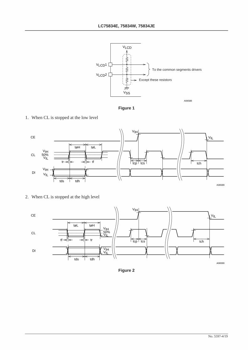
Figure 1
1. When CL is stopped at the low level
2. When CL is stopped at the high level
Figure 2
No. 5597-4/19
LC75834E, 75834W, 75834JE
VLCD1
VLCD2
VLCD
VSS
A06588
tøH tøL
tr tf
tds tdh
tcp tcs tch
VIL
VIH
VIH
VIH
VIL
VIL
50%CL
CE
DI
A06589
VIH
tøL tøH
tf tr
tds tdh
tcp tcs tch
VIL
VIH
VIH
VIL
VIL
50%CL
CE
DI
A06590
To the common segments drivers
Except these resistors
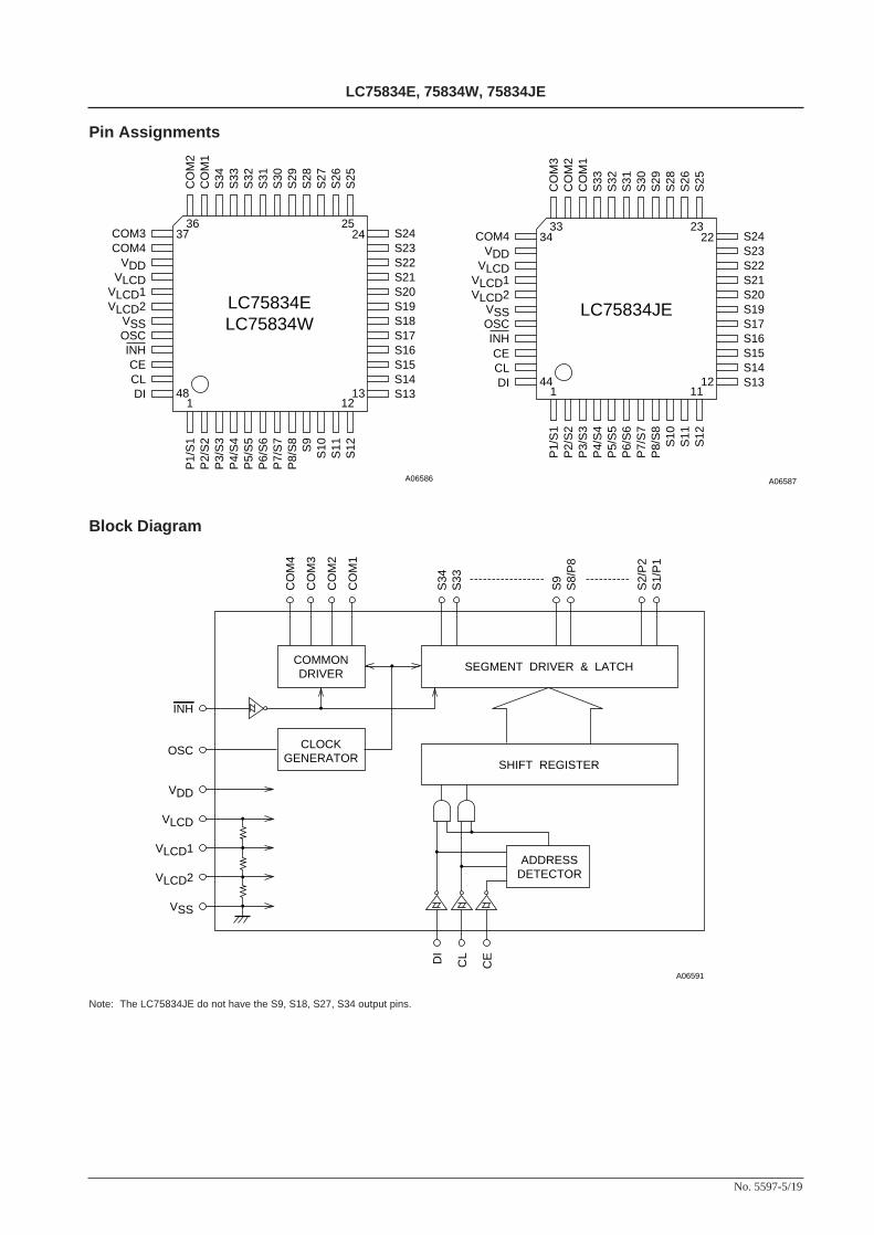
Pin Assignments
Block Diagram
Note: The LC75834JE do not have the S9, S18, S27, S34 output pins.
No. 5597-5/19
LC75834E, 75834W, 75834JE
COM3 37COM4
VDDVLCD
VLCD1VLCD2
VSSOSCINHCECLDI 48
S24S23S22S21S20S19S18S17S16S15S14S1313
24
P1/
S1
1 12
P2/
S2
P3/
S3
P4/
S4
P5/
S5
P6/
S6
P7/
S7
P8/
S8
S9
S10
S11
S12
S25
2536
S26
S27
S28
S29
S30
S31
S32
S33
S34
CO
M1
CO
M2
LC75834ELC75834W
A06586
COMMONDRIVER
ADDRESSDETECTOR
CLOCKGENERATOR
SEGMENT DRIVER & LATCH
SHIFT REGISTER
INH
OSC
VDD
VLCD
VLCD1
VLCD2
VSS
DI
CL
CE
CO
M4
CO
M3
CO
M2
CO
M1
S34
S33
S9
S8/
P8
S2/
P2
S1/
P1
A06591
34COM4VDD
VLCDVLCD1VLCD2
VSSOSCINHCECLDI 44
S24S23S22S21S20S19S17S16S15S14S1312
22
P1/
S1
1 11
P2/
S2
P3/
S3
P4/
S4
P5/
S5
P6/
S6
P7/
S7
P8/
S8
S10
S11
S12
2333
S25
S26
S28
S29
S30
S31
S32
S33
CO
M1
CO
M2
CO
M3
LC75834JE
A06587
Pin Functions
Note: The LC75834JE do not have the S9, S18, S27, S34 output pins.
No. 5597-6/19
LC75834E, 75834W, 75834JE
CE: Chip enableCL: Synchronization clockDI: Transfer data
H
—
S1/P1 toS8/P8
S9 to S34
Pin
1 to 8
9 to 34
LC75834E,75834W
LC75834JE
1 to 8
9 to 30— O Open
Segment outputs for displaying the display data transferred by serial datainput. The pins S1/P1 to S8/P8 can be used as general-purpose output portswhen so set up by the control data.
COM1 COM2COM3COM4
35363738
31323334
— O OpenCommon driver outputs. The frame frequency fO is given by: fO = (fOSC/512) Hz.
OSC 44 40
CECLDI
464748
424344
Serial data transfer inputs. Thesepins are connected to the controlmicroprocessor.
— I/O VDD
I GND
Oscillator connection An oscillator circuit is formed by connecting an external resistor and capacitorto this pin.
VLCD1 41 37 — I OpenUsed to apply the LCD drive 2/3 bias voltage externally. This pin must beconnected to VLCD2 when 1/2 bias drive is used.
VLCD2 42 38 — I OpenUsed to apply the LCD drive 1/3 bias voltage externally. This pin must beconnected to VLCD1 when 1/2 bias drive is used.
VDD 39 35 — — —Logic block power supply. Provide a voltage in the range 2.7 to 6.0 V.
VLCD 40 36 — — —LCD driver block power supply. Provide a voltage in the range 2.7 to 6.0 V.
VSS 43 39 — — —Ground pin. Connect to ground.
INH 45 41 L I GND
Display off control input•INH = low (VSS): Off
S1/P1 to S8/P8 = Low(These pins are forcible set to the segment output port function and fixed at the VSS level.) S9 to S34 = Low (VSS), COM1 to COM4 = Low (VSS)
•INH = high (VDD): OnNote that serial data transfers can be performed when the display is forced off by this pin.
Active I/OHandling
when unusedFunction
Pin No.
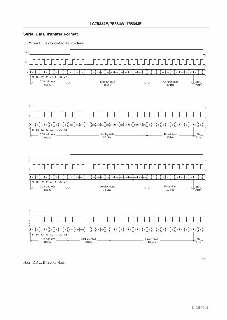
Serial Data Transfer Format
1. When CL is stopped at the low level
Note: DD ... Direction data
No. 5597-7/19
LC75834E, 75834W, 75834JE
CE
CL
DI 10 1 0 0 0 1 0
B1B0 B2 B3 A0 A1 A2 A3
D1 D2 D3 D25 D26 D27 D28 D29 D30 D31 D32 D33 D34 D35 D36 0 0 0 P0 P1 P2 P3 DR SC BU 0 0
10 1 0 0 0 1 0
B1B0 B2 B3 A0 A1 A2 A3
D37 D38 D39 D61 D62 D63 D64 D65 D66 D67 D68 D69 D70 D71 D72 0 0 0 0 0 0 0 0 0 0 0 1
10 1 0 0 0 1 0
B1B0 B2 B3 A0 A1 A2 A3
D73 D74 D75 D97 D98 D99 D100 D101 D102 D103 D104 D105 D106 D107 D108 0 0 0 0 0 0 0 0 0 0 1 0
10 1 0 0 0 1 0
B1B0 B2 B3 A0 A1 A2 A3
D109 D110 D111 D133 D134 D135 D136 0 0 0 0 0 0 0 0 0 0 0 0 0 0 0 0 0 0 1 1
A06592
CCB address8 bits
Display data36 bits
Control data10 bits
Fixed data10 bits
DD2 bits
CCB address8 bits
Display data36 bits
DD2 bits
CCB address8 bits
CCB address8 bits
Display data36 bits
Display data28 bits
Fixed data10 bits
Fixed data18 bits
DD2 bits
DD2 bits

2. When CL is stopped at the high level
Note: DD ... Direction data
• CCB address...............46H• D1 to D136.................Display data (At the LC75834JE, the display data D33 to D36, D69 to D72, D105 to D108,
D133 to D136 must be set to 0.• P0 to P3 ......................Segment output port/general-purpose output port switching control data• DR ..............................1/2 bias drive or 1/3 bias drive switching control data• SC...............................Segments on/off control data• BU ..............................Normal mode/power-saving mode control data
No. 5597-8/19
LC75834E, 75834W, 75834JE
CE
CL
DI 10 1 0 0 0 1 0
B1B0 B2 B3 A0 A1 A2 A3
D1 D2 D3 D25 D26 D27 D28 D29 D30 D31 D32 D33 D34 D35 D36 0 0 0 P0 P1 P2 P3 DR SC BU 0 0
10 1 0 0 0 1 0
B1B0 B2 B3 A0 A1 A2 A3
D37 D38 D39 D61 D62 D63 D64 D65 D66 D67 D68 D69 D70 D71 D72 0 0 0 0 0 0 0 0 0 0 0 1
10 1 0 0 0 1 0
B1B0 B2 B3 A0 A1 A2 A3
D73 D74 D75 D97 D98 D99 D100 D101 D102 D103 D104 D105 D106 D107 D108 0 0 0 0 0 0 0 0 0 0 1 0
10 1 0 0 0 1 0
B1B0 B2 B3 A0 A1 A2 A3
D109 D110 D111 D133 D134 D135 D136 0 0 0 0 0 0 0 0 0 0 0 0 0 0 0 0 0 0 1 1
A06593
CCB address8 bits
CCB address8 bits
CCB address8 bits
CCB address8 bits
Display data36 bits
Display data36 bits
Display data36 bits
Display data28 bits
Control data10 bits
Fixed data10 bits
Fixed data10 bits
Fixed data18 bits
DD2 bits
DD2 bits
DD2 bits
DD2 bits

Serial Data Transfer Examples
• At the LC75834E and LC75834W when109 or more segments are used, at the LC75834JE when 97 or more segmentsare used,192 bits of serial data must be sent.
Note: At the LC75834JE, the display data D33 to D36, D69 to D72, D105 to D108, D133 to D136 must be set to 0.
• At the LC75834E and LC75834W when used with less than 109 segments, at the LC75834JE when used with less than97 segments, transfer either 48 bits, 96 bits or 144 bits of serial data depending on the number of segments used.However, the serial data shown in the figure below (the display data D1 to D36 and the control data) must be sent.
Note: At the LC75834JE, the display data D33 to D36 must be set to 0.
Control Data Functions
1. P0 to P3: Segment output port/general-purpose output port switching control data.These control data bits switch the S1/P1 to S8/P8 output pins between their segment output port and general-purposeoutput port functions.
Note: Sn (n = 1 to 8): Segment output portsPn (n = 1 to 8): General-purpose output ports
No. 5597-9/19
LC75834E, 75834W, 75834JE
Control data Output pin states
P0 P1 P2 P3 S1/P1 S2/P2 S3/P3 S4/P4 S5/P5 S6/P6 S7/P7 S8/P8
0 0 0 0 S1 S2 S3 S4 S5 S6 S7 S8
0 0 0 1 P1 S2 S3 S4 S5 S6 S7 S8
0 0 1 0 P1 P2 S3 S4 S5 S6 S7 S8
0 0 1 1 P1 P2 P3 S4 S5 S6 S7 S8
0 1 0 0 P1 P2 P3 P4 S5 S6 S7 S8
0 1 0 1 P1 P2 P3 P4 P5 S6 S7 S8
0 1 1 0 P1 P2 P3 P4 P5 P6 S7 S8
0 1 1 1 P1 P2 P3 P4 P5 P6 P7 S8
1 0 0 0 P1 P2 P3 P4 P5 P6 P7 P8
0 1 1 0 0 0 1 0
B0 B1 B2 B3 A0 A1 A2 A3
D1 D2 D3 D25 D26 D27 D28 D29 D30 D31 D32 D33 D34 D35 D36 0 0 0 P0 P1 P2 P3 DR SC BU 0 0
A06595
0 1 1 0 0 0 1 0
B0 B1 B2 B3 A0 A1 A2 A3
D1 D2 D3 D25 D26 D27 D28 D29 D30 D31 D32 D33 D34 D35 D36 0 0 0 P0 P1 P2 P3 DR SC BU 0 0
0 1 1 0 0 0 1 0
B0 B1 B2 B3 A0 A1 A2 A3
D37 D38 D39 D61 D62 D63 D64 D65 D66 D67 D68 D69 D70 D71 D72 0 0 0 0 0 0 0 0 0 0 0 1
0 1 1 0 0 0 1 0
B0 B1 B2 B3 A0 A1 A2 A3
D73 D74 D75 D97 D98 D99 D100 D101 D102 D103 D104 D105 D106 D107 D108 0 0 0 0 0 0 0 0 0 0 1 0
0 1 1 0 0 0 1 0
B0 B1 B2 B3 A0 A1 A2 A3
D109 D110 D111 D133 D134 D135 D136 0 0 0 0 0 0 0 0 0 0 0 0 0 0 0 0 0 0 1 1
A06594
8 bits 48 bits
8 bits 48 bits
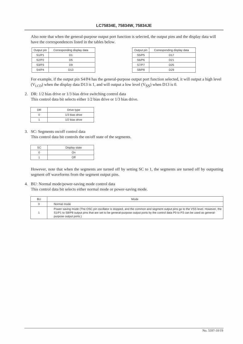
Also note that when the general-purpose output port function is selected, the output pins and the display data willhave the correspondences listed in the tables below.
For example, if the output pin S4/P4 has the general-purpose output port function selected, it will output a high level(VLCD) when the display data D13 is 1, and will output a low level (VSS) when D13 is 0.
2. DR: 1/2 bias drive or 1/3 bias drive switching control dataThis control data bit selects either 1/2 bias drive or 1/3 bias drive.
3. SC: Segments on/off control dataThis control data bit controls the on/off state of the segments.
However, note that when the segments are turned off by setting SC to 1, the segments are turned off by outputtingsegment off waveforms from the segment output pins.
4. BU: Normal mode/power-saving mode control dataThis control data bit selects either normal mode or power-saving mode.
No. 5597-10/19
LC75834E, 75834W, 75834JE
DR Drive type
0 1/3 bias drive
1 1/2 bias drive
SC Display state
0 On
1 Off
BU Mode
0 Normal mode
Power saving mode (The OSC pin oscillator is stopped, and the common and segment output pins go to the VSS level. However, the1 S1/P1 to S8/P8 output pins that are set to be general-purpose output ports by the control data P0 to P3 can be used as general-
purpose output ports.)
Output pin Corresponding display data
S1/P1 D1
S2/P2 D5
S3/P3 D9
S4/P4 D13
Output pin Corresponding display data
S5/P5 D17
S6/P6 D21
S7/P7 D25
S8/P8 D29
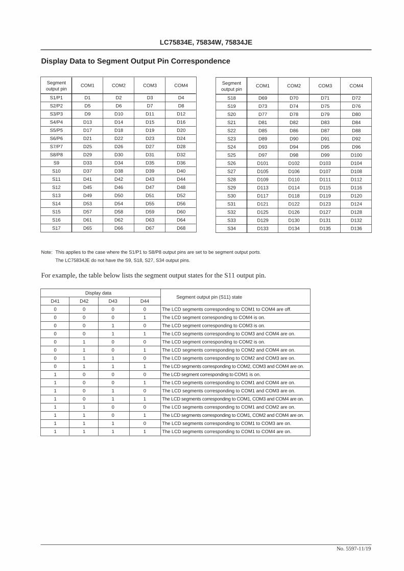
Display Data to Segment Output Pin Correspondence
Note: This applies to the case where the S1/P1 to S8/P8 output pins are set to be segment output ports.
The LC75834JE do not have the S9, S18, S27, S34 output pins.
For example, the table below lists the segment output states for the S11 output pin.
No. 5597-11/19
LC75834E, 75834W, 75834JE
Segment COM1 COM2 COM3 COM4output pin
S1/P1 D1 D2 D3 D4
S2/P2 D5 D6 D7 D8
S3/P3 D9 D10 D11 D12
S4/P4 D13 D14 D15 D16
S5/P5 D17 D18 D19 D20
S6/P6 D21 D22 D23 D24
S7/P7 D25 D26 D27 D28
S8/P8 D29 D30 D31 D32
S9 D33 D34 D35 D36
S10 D37 D38 D39 D40
S11 D41 D42 D43 D44
S12 D45 D46 D47 D48
S13 D49 D50 D51 D52
S14 D53 D54 D55 D56
S15 D57 D58 D59 D60
S16 D61 D62 D63 D64
S17 D65 D66 D67 D68
Segment COM1 COM2 COM3 COM4output pin
S18 D69 D70 D71 D72
S19 D73 D74 D75 D76
S20 D77 D78 D79 D80
S21 D81 D82 D83 D84
S22 D85 D86 D87 D88
S23 D89 D90 D91 D92
S24 D93 D94 D95 D96
S25 D97 D98 D99 D100
S26 D101 D102 D103 D104
S27 D105 D106 D107 D108
S28 D109 D110 D111 D112
S29 D113 D114 D115 D116
S30 D117 D118 D119 D120
S31 D121 D122 D123 D124
S32 D125 D126 D127 D128
S33 D129 D130 D131 D132
S34 D133 D134 D135 D136
Display dataSegment output pin (S11) state
D41 D42 D43 D44
0 0 0 0 The LCD segments corresponding to COM1 to COM4 are off.
0 0 0 1 The LCD segment corresponding to COM4 is on.
0 0 1 0 The LCD segment corresponding to COM3 is on.
0 0 1 1 The LCD segments corresponding to COM3 and COM4 are on.
0 1 0 0 The LCD segment corresponding to COM2 is on.
0 1 0 1 The LCD segments corresponding to COM2 and COM4 are on.
0 1 1 0 The LCD segments corresponding to COM2 and COM3 are on.
0 1 1 1 The LCD segments corresponding to COM2, COM3 and COM4 are on.
1 0 0 0 The LCD segment corresponding to COM1 is on.
1 0 0 1 The LCD segments corresponding to COM1 and COM4 are on.
1 0 1 0 The LCD segments corresponding to COM1 and COM3 are on.
1 0 1 1 The LCD segments corresponding to COM1, COM3 and COM4 are on.
1 1 0 0 The LCD segments corresponding to COM1 and COM2 are on.
1 1 0 1 The LCD segments corresponding to COM1, COM2 and COM4 are on.
1 1 1 0 The LCD segments corresponding to COM1 to COM3 are on.
1 1 1 1 The LCD segments corresponding to COM1 to COM4 are on.
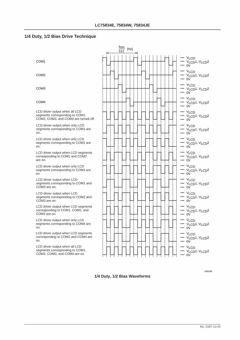
1/4 Duty, 1/2 Bias Drive Technique
No. 5597-12/19
LC75834E, 75834W, 75834JE
1/4 Duty, 1/2 Bias Waveforms
fosc512
[Hz]
COM1
COM2
COM3
COM4
VLCDVLCD1, VLCD20V
VLCDVLCD1, VLCD20V
VLCDVLCD1, VLCD20V
VLCDVLCD1, VLCD20V
VLCDVLCD1, VLCD20V
VLCDVLCD1, VLCD20V
VLCDVLCD1, VLCD20V
VLCDVLCD1, VLCD20V
VLCDVLCD1, VLCD20V
VLCDVLCD1, VLCD20V
VLCDVLCD1, VLCD20V
VLCDVLCD1, VLCD20V
VLCDVLCD1, VLCD20V
VLCDVLCD1, VLCD20V
VLCDVLCD1, VLCD20V
A06596
LCD driver output when all LCDsegments corresponding to COM1,COM2, COM3, and COM4 are turned off.
LCD driver output when only LCDsegments corresponding to COM1 areon.
LCD driver output when only LCDsegments corresponding to COM2 areon.
LCD driver output when only LCDsegments corresponding to COM4 areon.
LCD driver output when LCD segmentscorresponding to COM1 and COM2are on.
LCD driver output when only LCDsegments corresponding to COM3 areon.
LCD driver output when LCDsegments corresponding to COM1 andCOM3 are on.
LCD driver output when LCDsegments corresponding to COM2 andCOM3 are on.
LCD driver output when all LCDsegments corresponding to COM1,COM2, COM3, and COM4 are on.
LCD driver output when LCD segmentscorresponding to COM2 and COM4 areon.
LCD driver output when LCD segmentscorresponding to COM1, COM2, andCOM3 are on.

No. 5597-13/19
LC75834E, 75834W, 75834JE
1/4 Duty, 1/3 Bias Drive Technique
1/4 Duty, 1/3 Bias Waveforms
VLCDVLCD1VLCD20VVLCDVLCD1VLCD20VVLCDVLCD1VLCD20VVLCDVLCD1VLCD20VVLCDVLCD1VLCD20VVLCDVLCD1VLCD20VVLCDVLCD1VLCD20VVLCDVLCD1VLCD20VVLCDVLCD1VLCD20VVLCDVLCD1VLCD20VVLCDVLCD1VLCD20VVLCDVLCD1VLCD20VVLCDVLCD1VLCD20VVLCDVLCD1VLCD20VVLCDVLCD1VLCD20V
COM1
COM2
COM3
COM4
fosc512
[Hz]
A06597
LCD driver output when all LCDsegments corresponding to COM1,COM2, COM3, and COM4 are turned off.
LCD driver output when only LCDsegments corresponding to COM1 areon.
LCD driver output when only LCDsegments corresponding to COM2 areon.
LCD driver output when only LCDsegments corresponding to COM4 areon.
LCD driver output when LCD segmentscorresponding to COM1 and COM2 areon.
LCD driver output when only LCDsegments corresponding to COM3 areon.
LCD driver output when LCD segmentscorresponding to COM1 and COM3 areon.
LCD driver output when LCD segmentscorresponding to COM2 and COM3 areon.
LCD driver output when all LCDsegments corresponding to COM1,COM2, COM3, and COM4 are on.
LCD driver output when LCD segmentscorresponding to COM2 and COM4 areon.
LCD driver output when LCD segmentscorresponding to COM1, COM2, andCOM3 are on.
No. 5597-14/19
LC75834E, 75834W, 75834JE
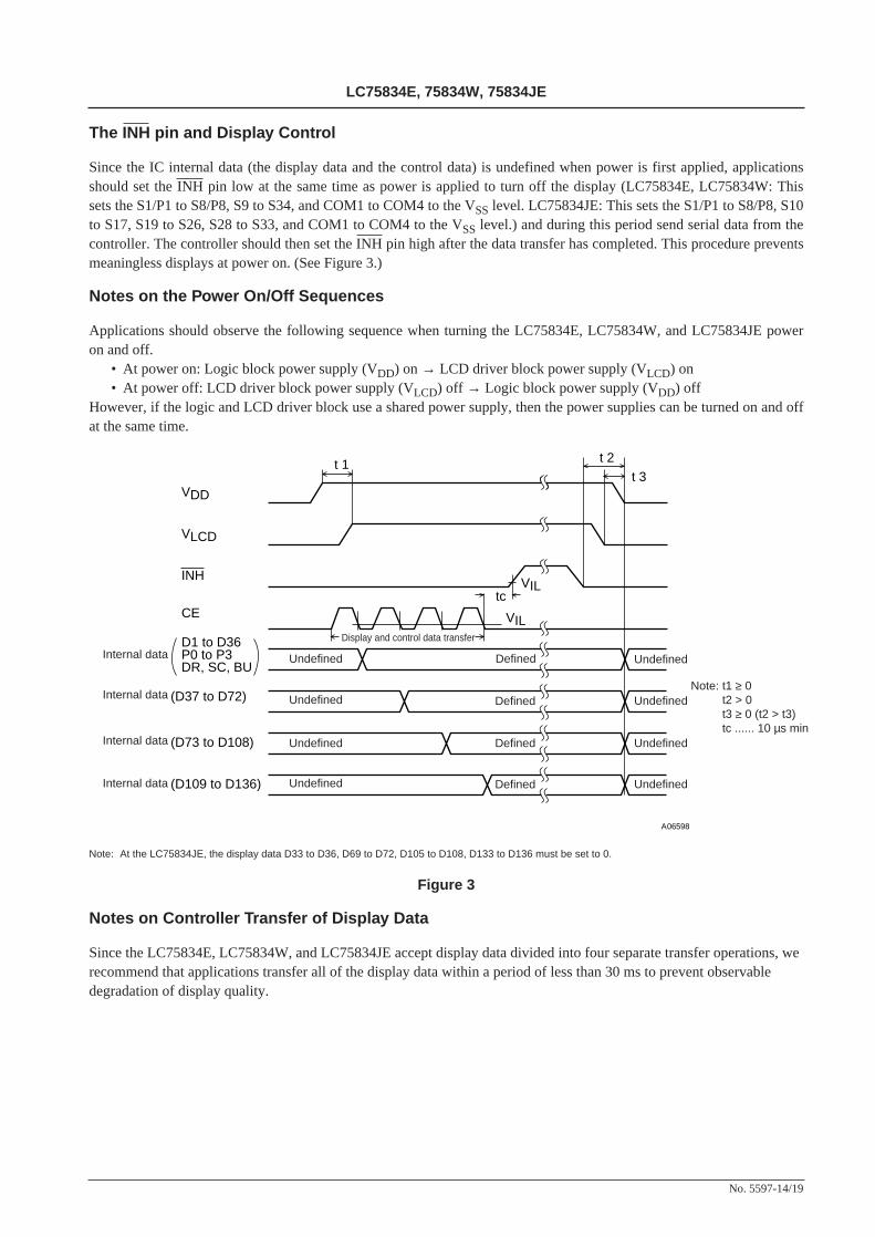
The INH pin and Display Control
Since the IC internal data (the display data and the control data) is undefined when power is first applied, applicationsshould set the INH pin low at the same time as power is applied to turn off the display (LC75834E, LC75834W: Thissets the S1/P1 to S8/P8, S9 to S34, and COM1 to COM4 to the VSS level. LC75834JE: This sets the S1/P1 to S8/P8, S10to S17, S19 to S26, S28 to S33, and COM1 to COM4 to the VSS level.) and during this period send serial data from thecontroller. The controller should then set the INH pin high after the data transfer has completed. This procedure preventsmeaningless displays at power on. (See Figure 3.)
Notes on the Power On/Off Sequences
Applications should observe the following sequence when turning the LC75834E, LC75834W, and LC75834JE poweron and off.
• At power on: Logic block power supply (VDD) on → LCD driver block power supply (VLCD) on• At power off: LCD driver block power supply (VLCD) off → Logic block power supply (VDD) off
However, if the logic and LCD driver block use a shared power supply, then the power supplies can be turned on and offat the same time.
Note: At the LC75834JE, the display data D33 to D36, D69 to D72, D105 to D108, D133 to D136 must be set to 0.
Figure 3
Notes on Controller Transfer of Display Data
Since the LC75834E, LC75834W, and LC75834JE accept display data divided into four separate transfer operations, werecommend that applications transfer all of the display data within a period of less than 30 ms to prevent observabledegradation of display quality.
VDD
VLCD
INH
CE
D1 to D36P0 to P3DR, SC, BU
(D37 to D72)
(D73 to D108)
t 1 t 2t 3
VILtc
VIL
(D109 to D136)
A06598
Internal data
Internal data
Undefined
Internal data
Internal data
Undefined
Undefined
Undefined
Undefined
Undefined
Undefined
Undefined
Defined
Defined
Defined
Defined
Display and control data transfer
Note: t1 ≥ 0t2 > 0t3 ≥ 0 (t2 > t3)tc ...... 10 µs min

Sample Application Circuit 1
1/2 Bias (for use with normal panels)• LC75834E, LC75834W
Note: *2 When a capacitor except the recommended external capacitance (COSC = 680 pF) is connected the OSC pin, we recommend that applications connect the OSC pin with a capacitor in the range 220 to 2200 pF.
• LC75834JE
Note: *2 When a capacitor except the recommended external capacitance (COSC = 680 pF) is connected the OSC pin, we recommend that applications connect the OSC pin with a capacitor in the range 220 to 2200 pF.
No. 5597-15/19
LC75834E, 75834W, 75834JE
VDD
VSS
VLCD
VLCD1
CVLCD2
INHCECLDI
COM1COM2COM3COM4P1/S1P2/S2
P8/S8S9
S32S33S34
+3 V
+5 V
C ≥ 0.047 µF
OSC
*2
(P1)(P2)
(P8)
A06599
VDD
VSS
VLCD
VLCD1
CVLCD2
INHCECLDI
COM1COM2COM3COM4P1/S1P2/S2
P8/S8S10
S17S19
S26S28
S33
+3 V
+5 V
C ≥ 0.047 µF
OSC
*2
(P1)(P2)
(P8)
A06600
From themicrocontroller
From themicrocontroller
General-purposeoutput ports
Used for functionssuch as backlightcontrol
LCD
pan
el (
up to
136
seg
men
ts)
General-purposeoutput ports
Used for functionssuch as backlightcontrol
LCD
pan
el (
up to
120
seg
men
ts)
No. 5597-16/19
LC75834E, 75834W, 75834JE
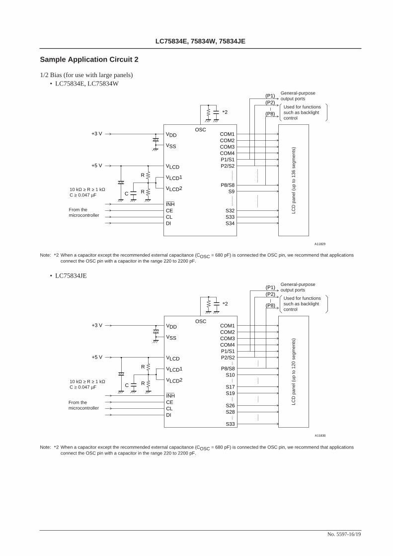
Sample Application Circuit 2
1/2 Bias (for use with large panels)• LC75834E, LC75834W
Note: *2 When a capacitor except the recommended external capacitance (COSC = 680 pF) is connected the OSC pin, we recommend that applications connect the OSC pin with a capacitor in the range 220 to 2200 pF.
• LC75834JE
Note: *2 When a capacitor except the recommended external capacitance (COSC = 680 pF) is connected the OSC pin, we recommend that applications connect the OSC pin with a capacitor in the range 220 to 2200 pF.
VDD
VSS
VLCD
VLCD1
C R
R
VLCD2
INHCECLDI
COM1COM2COM3COM4P1/S1P2/S2
P8/S8S9
S32S33S34
+3 V
+5 V
OSC
*2
(P1)(P2)
(P8)
A11829
From themicrocontroller
10 kΩ ≥ R ≥ 1 kΩC ≥ 0.047 µF
VDD
VSS
VLCD
VLCD1
VLCD2
INHCECLDI
COM1COM2COM3COM4P1/S1P2/S2
P8/S8S10
S17S19
S26S28
S33
+3 V
+5 V
OSC
*2
(P1)(P2)
(P8)
A11830
C R
R
10 kΩ ≥ R ≥ 1 kΩC ≥ 0.047 µF
From themicrocontroller
General-purposeoutput ports
Used for functionssuch as backlightcontrol
LCD
pan
el (
up to
136
seg
men
ts)
General-purposeoutput ports
Used for functionssuch as backlightcontrol
LCD
pan
el (
up to
120
seg
men
ts)
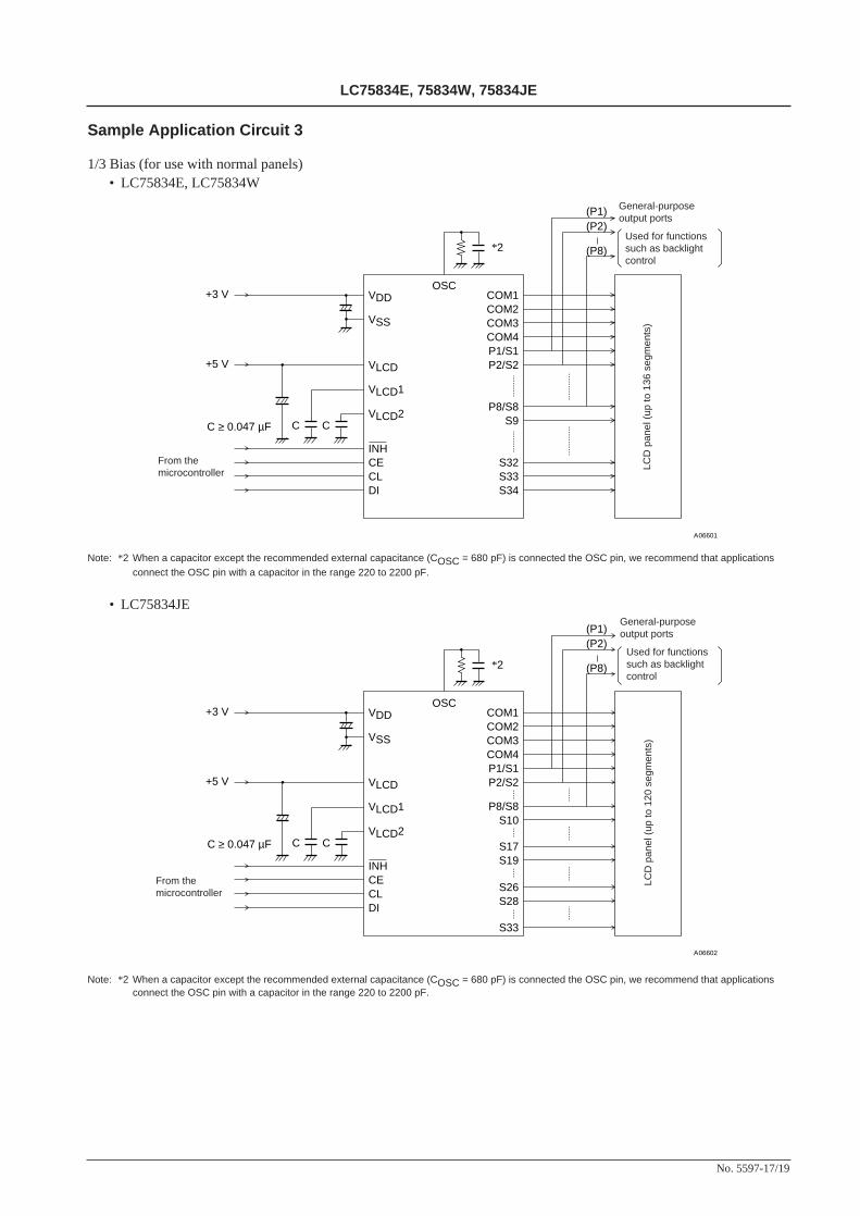
Sample Application Circuit 3
1/3 Bias (for use with normal panels)• LC75834E, LC75834W
Note: *2 When a capacitor except the recommended external capacitance (COSC = 680 pF) is connected the OSC pin, we recommend that applicationsconnect the OSC pin with a capacitor in the range 220 to 2200 pF.
• LC75834JE
Note: *2 When a capacitor except the recommended external capacitance (COSC = 680 pF) is connected the OSC pin, we recommend that applications connect the OSC pin with a capacitor in the range 220 to 2200 pF.
No. 5597-17/19
LC75834E, 75834W, 75834JE
VDD
VSS
VLCD
VLCD1
CVLCD2
INHCECLDI
COM1COM2COM3COM4P1/S1P2/S2
P8/S8S9
S32S33S34
+3 V
+5 V
C ≥ 0.047 µF
OSC
*2
(P1)(P2)
(P8)
A06601
C
VDD
VSS
VLCD
VLCD1
VLCD2
INHCECLDI
COM1COM2COM3COM4P1/S1P2/S2
P8/S8S10
S17S19
S26S28
S33
+3 V
+5 V
OSC
*2
(P1)(P2)
(P8)
A06602
CC ≥ 0.047 µF C
From themicrocontroller
From themicrocontroller
General-purposeoutput ports
Used for functionssuch as backlightcontrol
LCD
pan
el (
up to
136
seg
men
ts)
General-purposeoutput ports
Used for functionssuch as backlightcontrol
LCD
pan
el (
up to
120
seg
men
ts)

Sample Application Circuit 4
1/3 Bias (for use with large panels)• LC75834E, LC75834W
Note: *2 When a capacitor except the recommended external capacitance (COSC = 680 pF) is connected the OSC pin, we recommend that applications connect the OSC pin with a capacitor in the range 220 to 2200 pF.
Note: *2 When a capacitor except the recommended external capacitance (COSC = 680 pF) is connected the OSC pin, we recommend that applications connect the OSC pin with a capacitor in the range 220 to 2200 pF.
No. 5597-18/19
LC75834E, 75834W, 75834JE
VDD
VSS
VLCD
VLCD1
VLCD2
INHCECLDI
COM1COM2COM3COM4P1/S1P2/S2
P8/S8S9
S32S33S34
+3 V
+5 V
OSC
*2
(P1)(P2)
(P8)
A06603
C R
R
R
C
From themicrocontroller
10 kΩ ≥ R ≥ 1 kΩC ≥ 0.047 µF
VDD
VSS
VLCD
VLCD1
VLCD2
INHCECLDI
COM1COM2COM3COM4P1/S1P2/S2
P8/S8S10
S17S19
S26S28
S33
+3 V
+5 V
OSC
*2
(P1)(P2)
(P8)
A06604
C R
R
R
C
10 kΩ ≥ R ≥ 1 kΩC ≥ 0.047 µF
From themicrocontroller
• LC75834JE
General-purposeoutput ports
Used for functionssuch as backlightcontrol
LCD
pan
el (
up to
136
seg
men
ts)
General-purposeoutput ports
Used for functionssuch as backlightcontrol
LCD
pan
el (
up to
120
seg
men
ts)
PS No. 5597-19/19
LC75834E, 75834W, 75834JE
This catalog provides information as of October, 1999. Specifications and information herein are subjectto change without notice.
Specifications of any and all SANYO products described or contained herein stipulate the performance,characteristics, and functions of the described products in the independent state, and are not guaranteesof the performance, characteristics, and functions of the described products as mounted in the customer’sproducts or equipment. To verify symptoms and states that cannot be evaluated in an independent device,the customer should always evaluate and test devices mounted in the customer’s products or equipment.
SANYO Electric Co., Ltd. strives to supply high-quality high-reliability products. However, any and allsemiconductor products fail with some probability. It is possible that these probabilistic failures couldgive rise to accidents or events that could endanger human lives, that could give rise to smoke or fire,or that could cause damage to other property. When designing equipment, adopt safety measures sothat these kinds of accidents or events cannot occur. Such measures include but are not limited to protectivecircuits and error prevention circuits for safe design, redundant design, and structural design.
In the event that any or all SANYO products (including technical data, services) described or containedherein are controlled under any of applicable local export control laws and regulations, such products mustnot be exported without obtaining the export license from the authorities concerned in accordance with theabove law.
No part of this publication may be reproduced or transmitted in any form or by any means, electronic ormechanical, including photocopying and recording, or any information storage or retrieval system,or otherwise, without the prior written permission of SANYO Electric Co., Ltd.
Any and all information described or contained herein are subject to change without notice due toproduct/technology improvement, etc. When designing equipment, refer to the “Delivery Specification”for the SANYO product that you intend to use.
Information (including circuit diagrams and circuit parameters) herein is for example only; it is notguaranteed for volume production. SANYO believes information herein is accurate and reliable, butno guarantees are made or implied regarding its use or any infringements of intellectual property rightsor other rights of third parties.