lcm - newhaven display international, inc. · pdf file · 2014-03-17newhaven...
TRANSCRIPT

User’s Guide
NHD-320240WG-BxFMI-VZ#
LCM(Liquid Crystal Display Graphic Module)RoHS Compliant
NHD-320240-WG-B x- F-M-I-VZ#-
Newhaven Display 320 x 240 pixelsDisplay Type: GraphicModel serial number: B, x: New IC rev.White CCFL B/L STN-(negative) BlueTransmissive, 6:00 View, Wide Temperature (-20 ~ +70c)Negative voltage generator on board
For product support, contact
Newhaven Display International 2511 Technology Drive, #101 Elgin, IL 60124Tel: (847) 844-8795 Fax: (847) 844-8796
March 12, 2009

Newhaven Display International Page 2 of 18 NHD-320240-WG- B x F M I - V Z #
Contents
1. Module classification information
2. Precautions in Use of LCM
3. General Specification
4. Absolute Maximum Ratings
5. Electrical Characteristics
6. Optical Characteristics
7. Interface Description
8. Contour Drawing & Block Diagram
9. Timing Characteristics
10. Reliability
11. Backlight Information
12. Inspection specification

Newhaven Display International Page 3 of 18 NHD-320240-WG- B x F M I - V Z #
1.Module Classification Information
NHD 3 2 0 2 4 0 WG Bx F M I VZ#
� � � � ���
� Brand NEWHAVEN DISPLAY INTERNATIONAL, LLC.
� Display Font 320 * 240 Dots
� Display Type H Character Type, G Graphic Type
� Model serials number: B, x: New IC rev.
� Backlight Type N Without backlight
B EL, Blue green
D EL, Green
W EL, White
F CCFL, White
Y LED, Yellow Green
A LED, Amber
R LED, Red
O LED, Orange
G LED, Green
T LED, White
S LED, Bright White
� LCD Mode B TN Positive, Gray
N TN Negative,
G STN Positive, Gray
Y STN Positive, Yellow Green
T FSTN Negative
M STN Negative, Blue
F FSTN Positive
� LCD Polarizer Type/ Temperature range/ View direction
A Reflective, N.T, 6:00
D Reflective, N.T, 12:00
G Reflective, W. T, 6:00
J Reflective, W. T, 12:00
B Transflective, N.T,6:00
E Transflective, N.T.12:00
H Transflective, W.T,6:00
K Transflective,W.T,12:00
C Transmissive, N.T,6:00
F Transmissive, N.T,12:00
I Transmissive, W. T, 6:00
L Transmissive, W.T,12:00
Special Code VZ : Negative voltage generator on board # : RoHS Compliant

Newhaven Display International. Page 4 of 18 NHD-320240-WG- B x F M I - V Z #
2.Precautions in Use of LCD Module
(1)Avoid applying excessive shock to the module or making any alterations or modifications to it.
(2)Don’t make extra holes on the printed circuit board, modify its shape or change the components of
LCD Module.
(3)Don’t disassemble the LCM.
(4)Don’t operate it above the absolute maximum rating.
(5)Don’t drop, bend or twist LCM.
(6)Soldering: only to the I/O terminals.
(7)Storage: please store in anti-static electricity container and clean environment.
3.General Specification NHD-320240WG-BxFMI-VZ#
ITEM STANDARD VALUE UNIT
Number of dots 320x240 dots
Outline dimension 160.0(W)x 109.0(H)x 13.0max(T) mm
View area 122.0(W)x 92.0(H) mm
Active area 115.18(W)x 86.38(H) mm
Dot size 0.34(W)x 0.34(H) mm
Dot pitch 0.36(W)x 0.36(H) mm
LCD type STN- (negative) BLUE
View direction 6 o’clock
Backlight CCFL, White
Newhaven Display International Page 5 of 18 NHD-320240-WG - B x F M I - V Z #
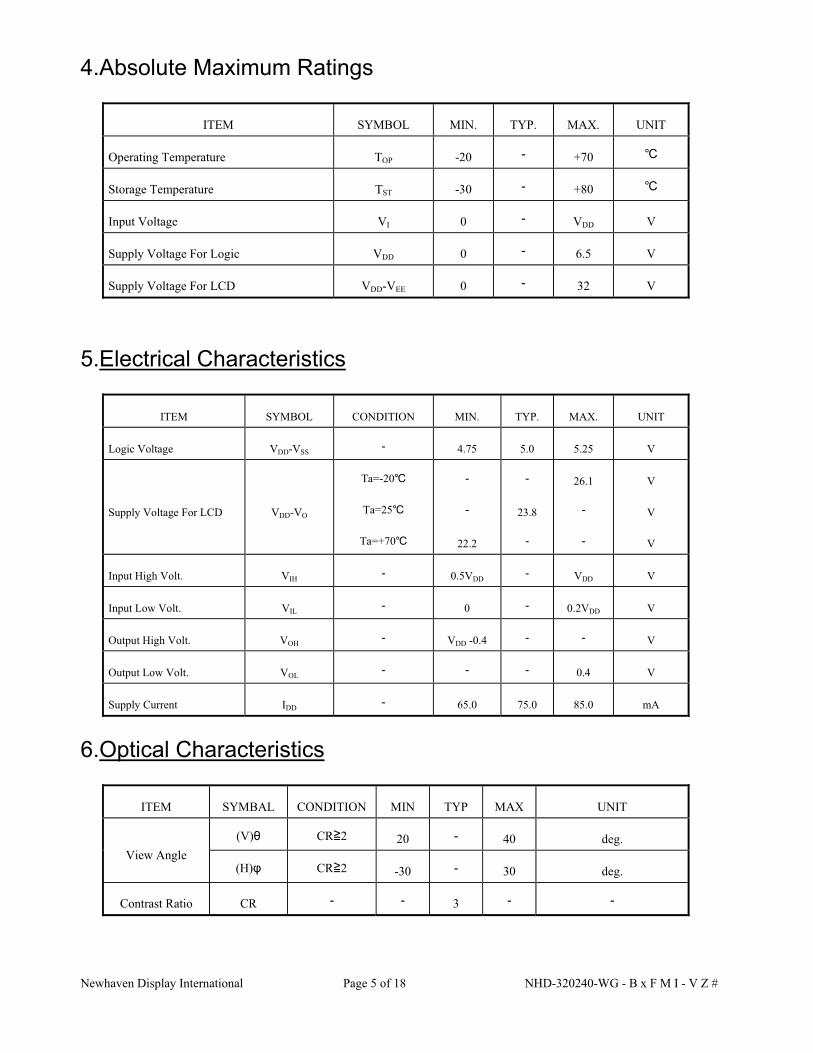
4.Absolute Maximum Ratings
ITEM SYMBOL MIN. TYP. MAX. UNIT
Operating Temperature TOP -20 +70
Storage Temperature TST -30 +80
Input Voltage VI 0 VDD V
Supply Voltage For Logic VDD 0 6.5 V
Supply Voltage For LCD VDD-VEE 0 32 V
5.Electrical Characteristics
ITEM SYMBOL CONDITION MIN. TYP. MAX. UNIT
Logic Voltage VDD-VSS 4.75 5.0 5.25 V
Supply Voltage For LCD VDD-VO
Ta=-20
Ta=25
Ta=+70 22.2
23.8
26.1 V
V
V
Input High Volt. VIH 0.5VDD VDD V
Input Low Volt. VIL 0 0.2VDD V
Output High Volt. VOH VDD -0.4 V
Output Low Volt. VOL 0.4 V
Supply Current IDD 65.0 75.0 85.0 mA
6.Optical Characteristics
ITEM SYMBAL CONDITION MIN TYP MAX UNIT
View Angle (V) CR 2 20 40 deg.
(H) CR 2 -30 30 deg.
Contrast Ratio CR 3

Newhaven Display International Page 6 of 17 NHD-320240-WG-BxFMI-VZ#
ITEM SYMBAL CONDITION MIN TYP MAX UNIT
(V) CR 2 20 40 deg. View Angle
(H) CR 2 -30 30 deg.
Contrast Ratio CR 3
T rise 200 300 ms Response Time
T fall 150 200 ms
6.1 Definitions
View Angles Contrast Ratio
Response time
Y
X
( Visual angle direction )ZBrightness at non-selected state ( Bns )Brightness at selected state ( BS )
Non-selected state
Operating voltage for LCD driving
CR =
Selected state
Brig
htne
ss (%
)
Bns
Bs
100
%
90 %
Rise Time Decay Time ( fall time tf )
Brig
htne
ss
Selected ConditionNonselected Condition Nonselected Condition
tr td
10 %

Newhaven Display International Page 7 of 18 NHD-320240-WG- B x F M I - V Z #
7.Interface Description
Pin No. Symbol Level Description
1 VSS 0V Ground
2 VDD 5.0V Power supply for Logic
3 VO (Variable) Driving voltage for LCD
4 A0 H/L RD=L WR=H ,A0=L :Data Read AO=H :Status read RD=H WR=L ,A0=L :Data Write AO=H :Command write
5 WR H/L 8080 family: Write signal, 6800 family: R/W signal
6 RD H/L 8080 family: Read signal, 6800 family: Enable clock
7~14 DB0~DB7 H/L Data bus line
15 CS H/L Chip select ,Active L
16 RES H/L Controller reset signal, Active L
17 Vee Negative Voltage Output
18 SEL 8088 or 6800 interface selection 1:68 0: 80
19 FG Frame Ground
20 WAIT Check Busy

Newhaven Display International. Page 8 of 18 NHD-320240-WG- B x F M I - V Z #
8.Contour Drawing & Block diagram
Pow
er O
NR
eset
*SEL1
CL1M
*:6800 family or 8080family interface selectable.
CSSED13700
Controller
CL2DB0~DB3
FLM
Vee
FGND Frame PAD
N.V.Generator
KA
LCM
B/L
LED B/L drive directlyfrom A,K .
R
MPU
Vdd
VR Vo10K~20K
-25V
Driver
Seg241~320Seg161~240
Driver
Seg81~160
Driver
Com
161~240C
om81~160
Driver
Driver
DB0~DB7A0
WRRD
Pow
er C
ircui
tB
ias a
nd
Com
1~80
Driver
RES
External contrast adjustment.
Seg1~80
Driver
320X240 DOT
101.0
109.0
0.5
4- 3.5
92.0(
VA)
8.5
25.0
320*240 Dots
1 CON2 20
SEL1
NCFGND
CSRESVee
151617181920
ZIF CONNECTORCOMPAREMOLEX-52207-2090
DB412
1413
WR
DB5
Vss1
RD7
1110
89
DB3DB2DB1DB0
4
65
32
DB6
A0Vo
Vdd
DOT SIZESCALE 10/1
DB7
0.34
0.34
0.36
28.41
11.04.0
11.31
86.38
(AA)
2.15
104.7
4.0
11.0MAX
1.06.5
165 0.5
LED B/L LED B/L
41.0
122.0(VA)
160.0 0.547.4
152.0141.0
115.18(AA)
0.36
CCFL B/L
190 5

Newhaven Display International Page 9 of 18 NHD-320240-WG-BxFMI-VZ#
9.Timing Characteristics
For relative timing diagram please see the spec of S1D13700.
9.1 Differences Between SED1335 and S1D13700
1 S1D13700 almost can replace SED1335 and it can drive 240*160 dots in 16 gray level, or
320*240 dots in 4 gray level.
2 There are 2 Main differences and being described as below:
(1) The Check Busy method of SED1335 is reading the D6 of STATUS resister.
Please
The Check Busy method of S1D13700 is checking the “WAIT” pin directly.

Newhaven Display International Page 10 of 18 NHD-320240-WG - B x F M I - V Z #
(2) Owing to S1D13700 having 32K*8 SRAM inside, so It doesn’t need to set the bit “M1” in
“SYSTEM SET”. For S1D13700, we doesn’t set M1 (bit1) the setting for SED 1335 is shown as
below:
The setting of S1D13700 will show as follow:

Newhaven Display International Page 11 of 18 NHD-320240W G - B x F M I - V Z #
10.RELIABILITYContent of Reliability Test (wide temperature, -20 ~70 )
Note1: No dew condensation to be observed.
Note2: The function test shall be conducted after 4 hours storage at the normal
Temperature and humidity after remove from the test chamber.
Note3: Vibration test will be conducted to the product itself without putting it in a container.
Environmental Test
Test Item Content of Test Test Condition Note
High Temperature storage Endurance test applying the high storage temperature for a
long time.
80
200hrs 2
Low Temperature
storage
Endurance test applying the high storage temperature for a
long time.
-30
200hrs 1,2
High Temperature
Operation
Endurance test applying the electric stress (Voltage &
Current) and the thermal stress to the element for a long time.
70
200hrs ——
Low Temperature
Operation
Endurance test applying the electric stress under low
temperature for a long time.
-20
200hrs 1
High Temperature/
Humidity Operation
The module should be allowed to stand at 60 ,90%RH max
For 96hrs under no-load condition excluding the polarizer,
Then taking it out and drying it at normal temperature.
60 ,90%RH
96hrs 1,2
Thermal shock resistance
The sample should be allowed stand the following 10 cycles of
operation -20 25 70
30min 5min 30min
1 cycle
-20 /70
10 cycles ——
Vibration test Endurance test applying the vibration during transportation
and using.
Total fixed amplitude :
15mm
Vibration Frequency :
10~55Hz
One cycle 60 seconds to
3 directions of X,Y,Z for
Each 15 minutes
3
Static electricity test Endurance test applying the electric stress to the terminal.
VS=800V,RS=1.5k
CS=100pF
1 time
——

Newhaven Display International, Page 16 of 16
16
11. Backlight Information
CCFL backlight Specification (AT=25 )
Specification Item Symbol Min Typ Max
Unit Condition
Luminance Frequency FL 40 50 60 KHZ
Tube current IL 3.5 5.0 6.5 mArms
Output Open Voltage VOpen 1100 Vrms No load voltage
Tube Voltage VLoadS 335 Vrms
Brightness B 2500 Cd/m2 IFL =5.0mArms
Brightness Uniformity Bu 75% % IFL =5.0mArms
Life time 50,000 hrs
CCFL Connector: XHP-3 (JST)

Newhaven Display International. Page 13 of 18 NHD-320240-WG- B x F M I - V Z #
12.Inspection specificationNO Item Criterion AQL
01 Electrical Testing
1.1 Missing vertical, horizontal segment, segment contrast defect. 1.2 Missing character, dot or icon. 1.3 Display malfunction. 1.4 No function or no display. 1.5 Current consumption exceeds product specifications. 1.6 LCD viewing angle defect. 1.7 Mixed product types. 1.8 Contrast defect.
0.65
02
Black or white spots on
LCD (display
only)
2.1 White and black spots on display 0.25mm, no more than three white or black spots present.
2.2 Densely spaced: No more than two spots or lines within 3mm 2.5
03
LCD black spots, white
spots,contaminati
on(non-display
)
3.1 Round type : As following drawing
2.5
3.2 Line type : (As following drawing) Length Width Acceptable Q TY
--- W Accept no dense
L 0.02 W2
L 0.03 W--- 0.05 W As round type
2.5
04 Polarizer bubbles
If bubbles are visible, judge using black spot specifications, not easy to find, must check in specify direction.
Size Acceptable Q TY
Accept no dense
3
2
0
Total Q TY 3
2.5

Newhaven Display International Page 14 of 18 NHD-320240-WG- B x F M I - V Z #
NO Item Criterion AQL
05 Scratches Follow NO.3 LCD black spots, white spots, contamination
06Chipped
glass
Symbols Define:
x: Chip length y: Chip width z: Chip thickness
k: Seal width t: Glass thickness a: LCD side length
L: Electrode pad length:
6.1 General glass chip :
6.1.1 Chip on panel surface and crack between panels:
2.5

Newhaven Display International Page 15 of 18 NHD-320240-WG- B x F M I - V Z #

Newhaven Display International Page 16 of 18 NHD-320240-WG- B x F M I - V Z #
NO Item Criterion AQL
06Glass
crack
x: Chip length y: Chip width z: Chip thickness k: Seal width t: Glass thickness a: LCD side length L: Electrode pad length 6.2 Protrusion over terminal : 6.2.1 Chip on electrode pad :
2.5
NO Item Criterion AQL
Newhaven Display International Page 17 of 18 NHD-320240-WG- B x F M I - V Z #
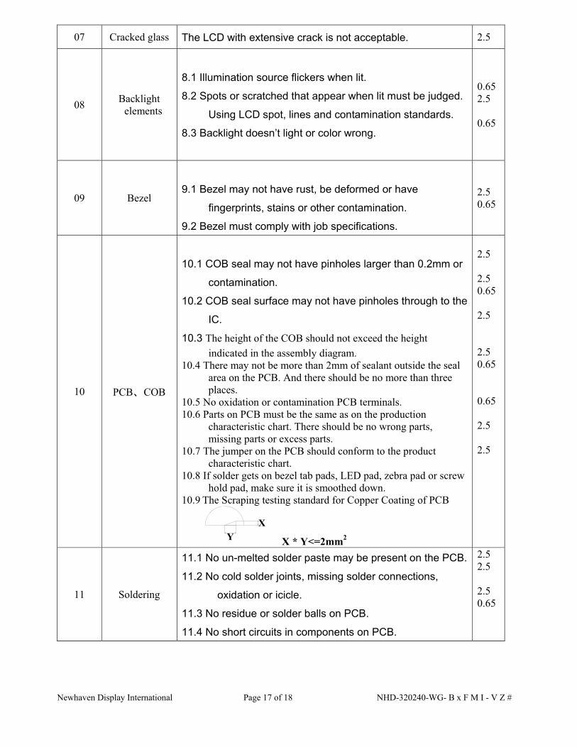
07 Cracked glass 2.5
08 Backlight elements
0.65 2.5
0.65
09 Bezel 2.5 0.65
10 PCB COB
The height of the COB should not exceed the height indicated in the assembly diagram.
10.4 There may not be more than 2mm of sealant outside the seal area on the PCB. And there should be no more than three places.
10.5 No oxidation or contamination PCB terminals. 10.6 Parts on PCB must be the same as on the production
characteristic chart. There should be no wrong parts, missing parts or excess parts.
10.7 The jumper on the PCB should conform to the product characteristic chart.
10.8 If solder gets on bezel tab pads, LED pad, zebra pad or screw hold pad, make sure it is smoothed down.
10.9 The Scraping testing standard for Copper Coating of PCB
YX
X * Y<=2mm2
2.5
2.5 0.65
2.5
2.5 0.65
0.65
2.5
2.5
11 Soldering
2.5 2.5
2.5 0.65

Newhaven Display International Page 18 of 18 NHD-320240-WG- B x F M I - V Z #
NO Item Criterion AQL
12General
appearance
2.5
0.65
2.5
2.5
2.5
2.5
2.5
0.65
0.65
0.65
0.65