lead-free solder bumping process for high temperature automotive
TRANSCRIPT

Lead-Free Solder Bumping Process for High Temperature Automotive Application
Thorsten Teutsch, Ronald G. Blankenhorn, Elke Zakel*
Pac Tech USA – Packaging Technologies, Inc. *Pac Tech – Packaging Technologies GmbH 328 Martin Avenue, Santa Clara, CA 95050 Am Schlangenhorst 15 -17, Germany Phone: (408) 588-1925 Phone: +49 (0)3321/4495 –0 Fax: (408) 588-1927 Fax: +49 (0)3321/4495 –23 e-mail: [email protected] e-mail: [email protected] http://www.pactech-usa.com http://www.pactech.de
Abstract In the last years low cost bumping techniques such as
electroless Nickel UBM followed by solder stencil printing have become accepted and established production processes for a manifold of applications (Passives, RFID, Memory, LCD, ASICS, etc) capable for wafer sizes up to 300 mm. [1]
Bumping processes, initially introduced to provide flip-chip capable devices with the main task of satisfying the increasing demand for cost-effective interconnection methods, and to take into account the ongoing need on further chip miniaturization, increasing I/O count and high frequency signal rate, must deal with the additional aspects on process technology and reliability.
Environmental and legal requirements on one side, and marketing aspects on the other side, are strongly demanding lead-free bumping and assembly solutions. Additionally, the higher melting point of the most common lead-free solder alloys is an interesting advantage with regard to high-temperature applications.
This paper is introducing based on electroless Ni/Au UBM a very cost competitive, lead-free solder stencil printing process for high temperature automotive applications - as one of the most toughest field of operation and qualification. [2] Initial capability studies are presented based on printing behavior of new solder paste materials of different alloys - SnAg4Cu0.5 and SnAg3.5 - with solder particle sizes of type 5 and type 6. Focusing on process qualification under production aspects a comparison of the obtained lead-free bumping results with state-of-the-art experimental data based on detailed process experiences with eutectic Sn37Pb63 is presented. Results of shear test, height distribution and yield data down to fine pitch (250 - 225 µm) pad layouts are shown.
The reflowed bump microstructure was examined due to intermetallic formation and UBM integrity by cross sectioning, SEM and EDX analysis. Reliability tests on 1st and 2nd level (T-cycling, T-storage and humidity tests) according automotive requirements have been also performed. Finally stencil printing design guidelines for wafer level stencil printing of lead-free solder pastes have been established.
Introduction
Driven by the need to achieve increased speed and performance along with higher I/O count flip-chip technology was introduced. However, one of the major breakthroughs is the use of flip-chip due to cost reduction. To accomplish this it is essential to use low-cost bumping techniques in combination with an assembly method compatible to existing SMT processes. For nearly all existing flip-chip techniques, a bump formation on the chip I/O is needed. Established techniques like the C4 process [3,4] do not fulfill the cost requirements for the low cost products. A selective chemical plating method can reduce bumping cost significantly since it does not require masking or metal sputtering. Additionally, this technique easily allows a parallel processing of multiple wafers, leading to a high throughput.
Behind this background, a low-cost bumping technology based on electroless Ni/Au and solder stencil printing is predestinated to serve the described requirements and emerging flip-chip market.
However, new product developments and process improvements are now approaching on flip-chip interconnection. These are being pushed by new demands of the semiconductor manufacturers, the assembly houses and the end users. Legal requirements caused by changes in the understanding of the protection of our environment in highly technologized nations have forced the development of lead-free manufacturing processes. Sales and marketing aspects are also promoting a lead-free (green) product line.
Not only flip-chip processes, but also the whole interconnection technology need to adjust to these tasks and provide new production solutions.
Beside the environmental requirements, technical aspects are demanding the development of sufficient lead-free solders. High-temperature applications such as “under-the-hood” electronics for automotive usage are taking advantage out of the synergy of lead-free alloys like SnAg and SnAgCu and their high-temperature capabilities to target the potential of a lead-free flip-chip process.
Electroless Nickel, as an cost-effective and innovative under bump metalization (UBM), has developed from a controversy discussed “newcomer” process for low-cost consumer electronics only into an established and reliable alternative to more costly processes (e.g. sputtering, electroplating). Meanwhile electroless Nickel production lines

are emerging at subcontractor facilities in the US, Europe, Asia and also worldwide at OEM sites providing an efficient UBM solution for Memory and LCD driver applications. At the moment the wafer-level CSP seems to be one of the fastest emerging applications for wafer. The feasibility and reliability of this bumping process has been proven in a series of published technical papers. [1,5,6,7,8]
Fig. 1: Ni/Au UBM (a) and Solder Bumps (b) Basically the Nickel bumps protect the Al and act as an
adhesion layer and a diffusion barrier and guarantee a stable and reliable contact to the Al bondpads [6,7]. Besides this, which is mainly the function of an under bump metallization the Ni can also offer a stand-off, e. g. for chip on glass (COG) using ACF [8]. Figure 1 shows SEM pictures of a typical Ni/Au bump for ultra-fine pitch LCD driver application (a) and eutectic SnPb solder bumps ontop of Ni UBM in 180 µm peripheral configuration (b).
To address the needs of automotive customers a production oriented capability study was performed using electroless Nickel as an UBM followed by lead-free solder application using stencil printing. Focussing on SnAg4Cu0.5 solders printing trials and optimization of the overall solder bumping process involving 1st level solder reflow and flux cleaning have been performed and analyzed under production aspects like: yield, solder height distribution and bump adhesion. A comparison to state-of-the-art stencil printing of eutectic Sn37Pb63 was also done.
Stencil Printing Two wafer types with two different layouts were selected
as test vehicle. Wafer I has a 6-inch size with 10 x 10mm dies and 225µm bond pad pitch in a peripheral configuration. The layout of wafer II (8-inch size) shows 5 x 5mm chips with 250µm bond pad pitch in area array configuration and a second chip type with six I/O’s only showing a 250µm pitch. The bond pad geometry, in both cases, has a round shape. The wetable UBM surface after Ni/Au bumping has a 90µm diameter. The total pad count per wafer is in a common range for wafer level stencil printing. An overview on the specification of the test vehicle is given in table 1. Both test layouts are advanced but feasible tasks for stencil printing of eutectic PbSn pastes and are already proven in mass production.
Wafer I Wafer II
Chip Type Area Array
6 I/O Peripheral
Pitch [µm] 250 250 225
UBM [µm] 90 90 90
Pads/chip 256 6 160
Pads/wafer 18.200 63.000
Tab. 1: Test Vehicle Specification Four different kinds if solder pastes have been selected
from three different suppliers. Their properties are listed in table 2. Using established process controls for solder paste quality, like solder balling test, measurement of solder particle distribution and characterization of the slumpy behavior, the different pastes were initially qualified to grant the quality consistency during printing.
Vendor Type Particle Size [µm]
Printing Quality
A 3 20-45 --
A 5 20-45 -
B 5 15-25 +/-
C 6 5-15 +
Tab. 2: Solder Paste Comparison
Figure 2 (a) shows the printing quality of a type 3 solder
paste, figure 2 (b) the printing quality of a type 5 solder paste. Only the type 6 solder paste with the smallest particle distribution was capable to provide sufficient printing quality (figure 2c). An overview on the printing behavior of the different solder paste materials is listed in the last column of table 2.
Fig. 2: Printing Results : Transfer Quality of Type 3 (a), Type 5 (b) and Type 6 (c) Solder Pastes Based on the printing trials with the test stencils for the
two different wafer layouts solder paste D was selected for complete process optimization including solder reflow and
(b) (a) (c)
(a) (b)

flux cleaning. Solder bridges and poor solder transfer quality were obtained as the main defects.
Introducing a special reflow process and the use of the reflow profile shown in figure 4 could solve initial problems due to incomplete solder reflow (figure 3). The flux residues and the solder satellites, after solder paste reflow, could only be removed sufficiently by using a newly developed cleaning process and a Megasonic process tank with a solvent-based flux cleaning solution.
Fig. 3: Insufficient Solder Reflow: Bump Shape (a) and
Evidence of Void Formation after Shear Test (b)
According to the obtained print quality the stencils were redesigned taking into account new aspect ratios with regard to stencil thickness and opening diameter. To achieve a better fine pitch capability and higher deposition volume of the solder paste, the new stencils were designed with square opening geometry. Finally, the internal stencil design rules and the wafer design requirements were revised [9]. After the stencil redesign the defect rate for solder bridges dropped to zero. Together with the usage of the type 6 solder paste of vendor C the occurrence of poor solder transfer was reduced significantly.
Fig. 4: Lead-free Reflow Profile
Results Once the solder bumping process (stencil design, solder
paste selection, printing, reflow and flux cleaning) was optimized, the achieved solder bump quality (see figure 5) was inspected using common process controls after printing of a significant number of wafers under production condition and
speed (~ 30 wafers/hour). Due to the tight pitch of the test wafer layout the stencil had to be cleaned after each print. For reference purpose, 2-3 test wafers have been bumped with eutectic SnPb solder paste.
Fig. 5: SnAg4Cu0.5 Solder Balls The obtained shear forces (table 3) show good bump
adhesion and no evidence for insufficient reflow conditions. The shear interface “bulk solder” is the first strong proof of the integrity and reliability of the Ni UBM. As expected, the shear force values of the lead-free solder bump alloy was higher, due to the harder material properties.
SnAg4Cu0.5 Sn37Pb63
Mean [µm]
Sigma [µm]
CPK Mean [µm]
Sigma [µm]
CPK
Wafer I
62.1 2.9 4.3 45.2 3.3 2.0
Wafer II
58.8 2.4 4.6 40.0 2.3 2.1
Tab. 3: Solder Bump Adhesion According to production requirements for solder bump
height distribution of +/- 15 µm @ 3 sigma the measured solder heights are listed in table 4 and are fully within the target specification.
SnAg4Cu0.5 Sn37Pb63
Target [µm]
Mean [µm]
Sigma [µm]
Mean [µm]
Sigma [µm]
Wafer I 95 99.0 6.44 95.9 5.2
Wafer II 100 111.7 5.7 100.7 7.2
Tab. 4: Solder Bump Height Overview However, the most convincing qualification data is always
the achieved bumping yield. Using a manual 100% optical inspection method (microscope) the bump yield loss was determined. The results were confirmed by additional measurements with a SISCAN fully automated inspection system from SIEMENS. It is shown clearly in table 5 that the impressive yield results for SnPb on both layouts cannot be
Reflow Profile SnAgCu Solder Paste
0
50
100
150
200
250
0 50 100 150 200
Time in Seconds
°C
SnAgCu
achieved for SnAgCu. Based on the lead-free paste properties - mainly viscosity – the yield results for a pitch of 250µm are even better than for the eutectic SnPb paste. For tighter pitches and therefore, smaller stencil openings the transfer behavior of the lead-free solder paste is getting worse. This has to be optimized together with the solder paste manufacturer, which is done in a series of test programs at the moment.
Bump Yield Loss [ppm]
SnAg4Cu0.5 Sn37Pb63
Wafer I 0 - 55 0 - 110
Wafer II 120 - 350 95 - 120
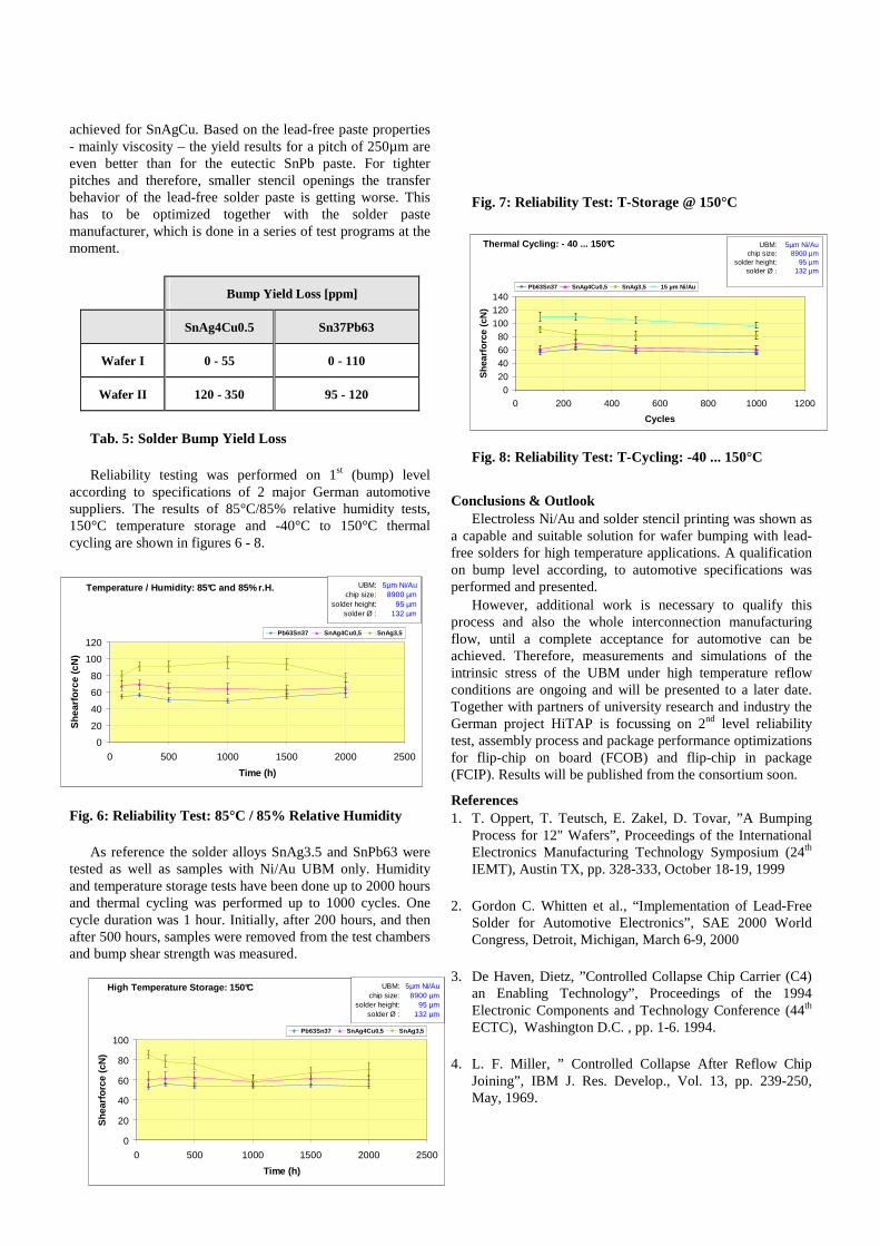
Tab. 5: Solder Bump Yield Loss Reliability testing was performed on 1st (bump) level
according to specifications of 2 major German automotive suppliers. The results of 85°C/85% relative humidity tests, 150°C temperature storage and -40°C to 150°C thermal cycling are shown in figures 6 - 8.
Fig. 6: Reliability Test: 85°C / 85% Relative Humidity
As reference the solder alloys SnAg3.5 and SnPb63 were
tested as well as samples with Ni/Au UBM only. Humidity and temperature storage tests have been done up to 2000 hours and thermal cycling was performed up to 1000 cycles. One cycle duration was 1 hour. Initially, after 200 hours, and then after 500 hours, samples were removed from the test chambers and bump shear strength was measured.
Fig. 7: Reliability Test: T-Storage @ 150°C
Fig. 8: Reliability Test: T-Cycling: -40 ... 150°C
Conclusions & Outlook Electroless Ni/Au and solder stencil printing was shown as
a capable and suitable solution for wafer bumping with lead-free solders for high temperature applications. A qualification on bump level according, to automotive specifications was performed and presented.
However, additional work is necessary to qualify this process and also the whole interconnection manufacturing flow, until a complete acceptance for automotive can be achieved. Therefore, measurements and simulations of the intrinsic stress of the UBM under high temperature reflow conditions are ongoing and will be presented to a later date. Together with partners of university research and industry the German project HiTAP is focussing on 2nd level reliability test, assembly process and package performance optimizations for flip-chip on board (FCOB) and flip-chip in package (FCIP). Results will be published from the consortium soon.
References 1. T. Oppert, T. Teutsch, E. Zakel, D. Tovar, ”A Bumping
Process for 12" Wafers”, Proceedings of the International Electronics Manufacturing Technology Symposium (24th IEMT), Austin TX, pp. 328-333, October 18-19, 1999
2. Gordon C. Whitten et al., “Implementation of Lead-Free
Solder for Automotive Electronics”, SAE 2000 World Congress, Detroit, Michigan, March 6-9, 2000
3. De Haven, Dietz, ”Controlled Collapse Chip Carrier (C4)
an Enabling Technology”, Proceedings of the 1994 Electronic Components and Technology Conference (44th ECTC), Washington D.C. , pp. 1-6. 1994.
4. L. F. Miller, ” Controlled Collapse After Reflow Chip
Joining”, IBM J. Res. Develop., Vol. 13, pp. 239-250, May, 1969.
Pb63Sn37 SnAg4Cu0,5 SnAg3,5100 53,06 2,39 60,8 6,73 84,94 4,04250 55,53 2,11 61,92 5,83 78,43 6,38500 53,82 2,37 62,23 5,3 76,15 6,16
1000 54,04 1,93 57,82 6,95 59,03 5,781500 54,44 1,91 61,38 5,14 66,26 62000 53,68 1,9 60,63 3,68 69,97 6,32
High Temperature Storage: 150°C
0
20
40
60
80
100
0 500 1000 1500 2000 2500
Time (h)
She
arfo
rce
(cN
)
Pb63Sn37 SnAg4Cu0,5 SnAg3,5
UBM: chip size:
solder height:solder Ø :
5µm Ni/Au8900 µm
95 µm132 µm
Pb63Sn37 SnAg4Cu0,5 SnAg3,5100 54,6 2,87 67,02 6,73 79,44 5,75250 56,37 2,7 68,54 5,83 90,03 5,34500 50,44 2,62 64,49 5,3 90,64 7,08
1000 49,24 2,46 63,56 6,95 95,49 7,181500 54,9 3,47 62,73 5,14 93,56 6,72000 58,14 4,57 65,18 7,19 77,47 5,58
Temperature / Humidity: 85°C and 85% r.H.
0
20
40
60
80
100
120
0 500 1000 1500 2000 2500
Time (h)
She
arfo
rce
(cN
)
Pb63Sn37 SnAg4Cu0,5 SnAg3,5
UBM: chip size:
solder height:solder Ø :
5µm Ni/Au8900 µm
95 µm132 µm
Pb63Sn37 SnAg4Cu0,5 SnAg3,5 15 µm Ni/Au102 56.35 2.6 61.92 4.25 90.92 4.34 109.79 6.06250 61.82 1.96 69.39 4.87 82.62 6.2 109.05 4.81500 56.96 1.93 62.38 4.62 81.22 6.5 103.98 4.79
1000 56.38 2.84 60.75 5.74 81.37 5.8 96.44 4.27
Thermal Cycling: - 40 ... 150°C
020406080
100120140
0 200 400 600 800 1000 1200
Cycles
She
arfo
rce
(cN
)
Pb63Sn37 SnAg4Cu0,5 SnAg3,5 15 µm Ni/Au
UBM: chip size:
solder height:solder Ø :
5µm Ni/Au8900 µm
95 µm132 µm

5. T. Oppert, E. Zakel, T. Teutsch, ”A Roadmap to Low Cost Flip Chip and CSP using Electroless Ni/Au”, Proceedings of the International Electronics Manufacturing Technology Symposium (IEMT) Symposium, Omiya, Japan, April 15-17, 1998
6. T. Oppert, E. Zakel, T. Teutsch, ”A Roadmap to Low
Cost Flip Chip and CSP using Electroless Ni/Au”, Proceedings of the IEMT/IMC Symposium, Omiya, Japan, April 15-17, 1998
7. G. Motulla et al., ”A Low Cost Bumping Service Based on
Electroless Nickel and Solder Printing"”, Proceedings of the IEMT/IMC Symposium, Omiya, Japan, April 16-18, 1997
8. M. Vrana, J. De Baets, A. Van Calster, D. Wojciechowski,
A. Ostmann, H. Reichl, ” An Anisotropic Adhesive Flip Chip Technology for LCD Drivers”, Proceedings of the SID Conference 1996
9. Pac Tech Webpage: www.pactech.de