leakage in nanometer cmos...
TRANSCRIPT
LEAKAGE IN NANOMETER CMOS TECHNOLOGIES

SERIES ON INTEGRATED CIRCUITS AND SYSTEMS
Anantha Chandrakasan, Editor Massachusetts Institute of Technology
Cambridge, Massachusetts, USA
Published books in the series;
A Practical Guide for SystemVerilog Assertions Srikanth Vijayaraghavan and Meyyappan Ramanathan
2005, ISBN 0-387-26049-8
Statistical Analysis and Optimization for VLSI: Timing and Power Ashish Srivastava, Dennis Sylvester and David Blaauw
2005, ISBN 0-387-25738-1
Leakage in Nanometer CMOS Technologies Siva G. Narendra and Anantha Chandrakasan
2005, ISBN 0-387-25737-3

LEAKAGE IN NANOMETER CMOS TECHNOLOGIES
Siva G. Narendra Tyfone, Inc.
Anantha Chandrakasan Massachusetts Institute of Technology
Springer

Library of Congress Cataloging-in-Publication Data
A C.I.P. Catalogue record for this book is available from the Library of Congress.
ISBN-10: 0-387-25737-3 ISBN-10: 0-387-28133-9 (e-book) ISBN-13: 9780387257372 ISBN-13: 9780387281339
Printed on acid-free paper.
© 2006 Springer Science+Business Media, Inc. All rights reserved. This work may not be translated or copied in whole or in part without the written permission of the publisher (Springer Science+Business Media, Inc., 233 Spring Street, New York, NY 10013, USA), except for brief excerpts in connection with reviews or scholarly analysis. Use in connection with any form of information storage and retrieval, electronic adaptation, computer software, or by similar or dissimilar methodology now known or hereafter developed is forbidden. The use in this publication of trade names, trademarks, service marks and similar terms, even if they are not identified as such, is not to be taken as an expression of opinion as to whether or not they are subject to proprietary rights.
Printed in the United States of America.
9 8 7 6 5 4 3 2 1 SPIN 11380634
springeronline.com
The contributing authors of this book have used figures and content published in IEEE conferences and journals (© IEEE). Those figures and content from IEEE publications that are included in this book are printed with permission from the IEEE.
Contents
Preface ix
1. Taxonomy of Leakage: Sources, Impact, and Solutions
1.1 Introduction 1.2 Sources 1.3 Impact 1.4 Solutions
References
2. Leakage Dependence on Input Vector SIVA NARENDRA, YIBIN YE, SHEKAR BORISAR, VIVEK DE, AND ANANTHA CHANDRAKASAN
2.1 Introduction 2.2 Stack Effect 2.3 Leakage Reduction using Natural Stacks 2.4 Leakage Reduction using Forced Stacks 2.5 Summary
References
3. Power Gating and Dynamic Voltage Scaling BENTON CALHOUN, JAMES IWO, AND ANANTHA CHANDRAKASAN
3.1 Introduction 3.2 Power Gating
1 3
11 13 18
21 23 30 35 38 39
41 41
Vi Leakage in Nanometer CMOS Technologies
3.3 Dynamic Voltage Scaling 64 3.4 Summary 73
References 73
4. Methodologies for Power Gating KIMIYOSHI USAMI AND TAKAYASU SAKURAI 4.1 Introduction 4.2 Power Gating Methodologies for Real Designs 4.3 Future Directions of Power Gating 4.4 Summary
References
5. Body Biasing TADAHIRO KURODA AND TAKAYASU SAKURAI 5.1 Introduction 5.2 Reverse Body Bias 5.3 Forward Body Bias 5.4 Future Directions
References
6. Process Variation and Adaptive Design SIVA NARENDRA, JAMES TSCHANZ, JAMES KAO, SHEKAR BORKAR, ANANTHA CHANDRAKASAN, AND VIVEK DE
6.1 Introduction 6.2 Bi-directional Adaptive Body Bias 6.3 Body Bias Circuit Impedance 6.4 Adaptive Supply Voltage and Adaptive Body Bias
References
7. Memory Leakage Reduction TAKAYUKI KAWAHARA AND KIYOO ITOH 7.1 Introduction 7.2 Leakage in RAMS 7.3 Leakage Sources and Reduction in RAMS 7.4 Various Leakage Reduction Schemes 7.5 Gate-Source Reverse Biasing Schemes 7.6 Applications to RAM Cells 7.7 Applications to Peripheral Circuits 7.8 Future Prospects 7.9 Conclusion
References
77 79 90
102 103
105 107 126 137 139
141 143 150 156 162
163 164 168 171 175 180 186 195 196 196
Leakage in Nanometer CA4OS Technologies vii
8. Active Leakage Reduction and Multi-Performance Devices
SIVA NARENDRA, JAMES TSCHANZ, SHEKAR BORKAR, AND VIVEK DE 8.1 Introduction 8.2 Standby Techniques for Active Leakage Reduction 8.3 Multi-performance Devices
References
9. Impact of Leakage Power and Variation on Testing AL1 KESHAVARZI AND KAUSHIK ROY
9.1 Introduction 9.2 Background 9.3 Leakage vs. Frequency Characterization 9.4 Multiple-Parameter Testing 9.5 Sensitivity Gain with RBB and Temperature 9.6 Leakage versus Temperature Two-Parameter Test Solution 9.7 Discussions and Test Applications 9.8 Conclusion
References
10. Case Study: Leakage Reduction in Hitachi/Renesas Microprocessors
MASAYUKI MIYAZAKI, HIROYUKI MIZUNO, AND TAKAYUKI KAWAHARA 10.1 Leakage Reduction Using Body Bias in a RISC
Microprocessor 10.2 Leakage Reduction in Application Processor in 3G
Cellular Phone 10.3 Leakage Reduction in SRAM module
References
11. Case Study: Leakage Reduction in the Intel Xscale Microprocessor
LAWRENCE CLARK 11.1 Introduction 11.2 Circuit Configuration and Operation 11.3 Regulator Design 11.4 Time-Division Multiplexed Operation 11.5 SOC Design Issues and Future Trends 11.6 Conclusion
201 202 208 209
211 212 214 216 218 227 229 232 232
235
240
249 255
257 261 267 273 276 278
. . . Vlll
References 279
12 . Transistor Design to Reduce Leakage
Leakage in Nanometer CMOS Technologies
SAGAR SUTHRAM, SIVA NARENDRA, AND SCOTT THOMPSON 12.1 12.2
12.3
12.4
12.5 12.6
12.7 12.8
Introduction Sub-threshold Leakage in Nanoscale Planar Si MOSFETs SiON Dielectrics to Reduce Gate to Channel Direct Tunneling Current Offset Spacers to Reduce Edge Direct Tunneling Current Compensation Implants to Reduce Junction Leakage Source/Drain Extension Grading to Reduce Gate Induced Drain Leakage (GIDL) Future Solutions Summary References
281 282
286
286
287 289
291 298 298
Index 301
Preface
Scaling transistors into the nanometer regime has resulted in a dramatic increase in MOS leakage (i.e., off-state) current. Threshold voltages of transistors have scaled to maintain performance at reduced power supply voltages. Leakage current has become a major portion of the total power consumption, and in many scaled technologies leakage contributes 30-50% of the overall power consumption under nominal operating conditions. Leakage is important in a variety of different contexts. For example, in desktop applications, active leakage power (i.e., leakage power when the processor is computing) is becoming significant compared to switching power. In battery operated systems, standby leakage (i.e., leakage when the processor clock is turned off) dominates as energy is drawn over long idle periods.
Increased transistor leakages not only impact the overall power consumed by a CMOS system, but also reduce the margins available for design due to the strong relationship between process variation and leakage power. It is essential for circuit and system designers to understand the components of leakage, sensitivity of leakage to different design parameters, and leakage mitigation techniques in nanometer technologies. This book provides an in-depth treatment of these issues for researchers and product designers.
This book also provides an understanding of various leakage power sources in nanometer scale MOS transistors. Leakage sources at the MOS transistor level including sub-threshold, gate tunneling, and junction currents will be discussed. Manifestation of these MOS transistor leakage components at the full chip level depends considerably on several aspects including the nature of the circuit block, its state, its application workload, and process/voltage/temperature conditions. The sensitivity of the various MOS

X Leakage in Nanometer CMOS Technologies
leakage current sources at the transistor level to these conditions will be introduced. These leakage currents at the transistor level translate at the system level in various ways and therefore impact the overall system in a diverse manner. For example, transistor leakages manifest differently under normal operation compared to typical testing conditions, such as burn-in testing. Transistor leakages impact power consumption of the system depending on the system state (e.g., active condition vs. standby condition). Active system leakage power can be significantly higher than standby system leakage, due to elevated temperature and the difficulty to trade-off leakage power for performance. The impact of leakage components also depends on the style of circuit and module type (e.g., memory vs. logic).
To deal with transistor leakage, a variety of solutions is required at all levels of design. The solutions include leakage modeling and prediction, transistor modifications, circuit techniques and system modifications. This book provides an in-depth coverage of promising techniques at the transistor, circuit, and architecture levels of abstraction.
The topics discussed in this book include sources of transistor leakage and its impact, state assignment based leakage reduction, power gating techniques, dynamic voltage scaling, body-biasing, use of multiple performance transistors, leakage reduction in memory, impact of process variation on leakage and design margins, active leakage power reduction techniques, and impact of process variation and leakage on testing. Additionally, two case studies will be presented to highlight real world examples that reap the benefits of leakage power reduction solutions. The last chapter of the book will highlight transistor design choices to mitigate the increase in the leakage components as technology continues to scale.
This book would not have been possible without the concerted effort of all its contributing authors. We would like to thank them for their contribution and help with reviewing other chapters to ensure consistency. We would also like to express sincere thanks to non-contributing reviewers -Dinesh Somashekar and Keith Bowman, both of Intel Corporation. I (Siva) would like to recognize the dedicated contribution of my late colleague and friend at Intel Corporation, Brad Bloechel, without whom, lot of the experimental results in the chapters 2, 6, 8, and 9 would not have been possible. He will be missed. Finally, we want to thank our families for their patience and support through the process of compiling this book together.
Siva G. Narendra Tyfone, Inc.
Anantha Chandrakasan Massachusetts Institute of Technology

Chapter 1
TAXONOMY OF LEAKAGE: SOURCES, IMPACT, AND SOLUTIONS
1.1 INTRODUCTION
Benefits of CMOS technology scaling in the nanometer regime comes with the disruptive consequence of increasing MOS transistor leakages. This increase in transistor leakages not only impacts the overall power consumption of a CMOS system, but also reduces the allowed design margins due to the strong relationship between process variation and leakage power. Therefore to continue to reap the benefits of technology scaling, it is essential for circuit designer and system architects to understand the sources of leakage, its impact on circuit and system designs, and solutions to minimize the impact of leakage in such designs. To effectively deal with the impact on circuit and system designs due to leakage, designers need to utilize prediction, reduction, adaptation, and administration techniques.
In this chapter, facts on why leakage power sources are becoming increasingly relevant in CMOS systems that use nanometer scale MOS transistors will be clarified. Leakage sources at the MOS transistor level including sub-threshold diffusion current, gate and junction tunneling currents will be discussed.
These leakage currents at the transistor level manifest themselves in various ways and impact the overall system in a diverse manner. For example, transistor leakages manifest themselves differently under normal operation compared to typical testing conditions, such as bum-in testing. Transistor leakages also impact power consumption of the system differently depending on if the system is in active condition compared or standby condition, as will become obvious later. In a given technology generation, impact of leakage components depends on the style of circuit, such as memory or logic. Additionally the impact on the circuit and systems depends on environmental conditions such as process comer, power supply voltage, and temperature of operation. In this chapter we will explain in further detail the diverse impact transistor leakages have on circuit and systems.

2 Leakage in Nanometer CMOS Technologies
To deal such diverse range of impacts due to transistor leakages, a variety of solutions is required at all levels of design. The solutions constitute leakage prediction, reduction, adaptation, and administration techniques.
By the nature of its origin MOS transistor leakage components in nanometer technologies depend exponentially on parameters, such as oxide thickness, channel length, temperature, and supply voltage. Given that leakage power is expected to become or has already become a significant portion of the total power it is imperative to predict system leakage in the presence of variation in transistor and environmental parameters. In this chapter a statistical approach to predict system leakage will also be introduced.
ircuit & Syste^l^ 2 ^
C Prediction ._2 Reduction ^ Adaptation O Administration C/)
i Figure 1-1. Taxonomy of leakage - sources, its impact, and solutions to reduce the impact. Sources originate at the transistor level influenced by the environment. Impact of the sources manifest in various ways at the circuit and system levels. Solutions can be implemented at the transistor, circuit, or system levels. Reduction and adaptation techniques help minimize the impact; prediction helps understand the source and nature of its impact; and administration helps administer and manage an array of solutions.
Reduction of leakage has to be addressed at all levels of the design hierarchy - transistor, circuit, and system. Techniques such as state assignment based leakage reduction, power gating techniques, dynamic voltage scaling, substrate-biasing, use of multiple performance transistors, leakage reduction in memory, active leakage power reduction techniques, and transistor design choices will explained in detailed in dedicated chapters.
Since leakage depends exponentially on several transistor and environmental parameters, it is becoming harder to meet the required system specifications, such as power and performance, over the entire range of these parameters. Adaptation of the system to changes in these parameters helps

1. Taxonomy of Leakage 3
reduce the impact leakage will have on the design margin. Techniques such as adaptive body bias and adaptive supply voltage will be discussed in detail in latter chapters. Impact of process variation and leakage on testing, and two case studies to highlight real world examples that reap the benefits of leakage reduction solutions will also be discussed.
While administration is not specifically discussed in the book, this is an important aspect of all leakage reduction techniques. It should be clear that there is no single technique that solves all the impacts of leakage. An array of techniques is required and administration of these techniques will be essential to provide effective leakage reduction. Administration includes tools to evaluate the benefits of a technique; tools to productively implement the technique; design, silicon space, and testing resources to put the technique into practice. The two case studies covered will provide examples of aspects of solution administration. The taxonomy of leakage as dealt in this book is illustrated in Figure 1-1.
1.2 SOURCES
To understand the sources of leakage components at the MOS transistor level, it is important to appreciate how transistors and systems that use them have evolved over time to follow Moore's law [1]. MOS transistor based integrated circuits have transformed the world we live in. It is estimated that there are more than 15 billion silicon semiconductor chips currently in use with an additional 500,000 sold each day [2].
The ever shrinking size of the MOS transistors that result in faster, smaller, and cheaper systems have enabled ubiquitous use of these chips. The requisite to continually follow Moore's law and reap its associated benefits is making leakage sources to be more relevant than before. Let us look at the evolution of semiconductor chips that use MOS transistors as the building block.
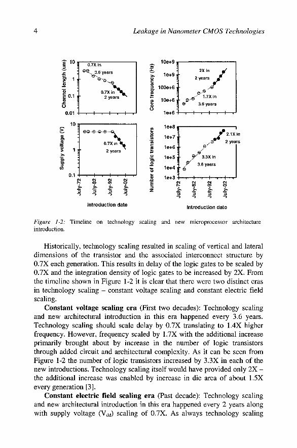
Among these semiconductor chips, a prevalent component is the high-performance general-purpose microprocessor. Figure 1-2 illustrates the timeline on technology scaling and new high-performance microprocessor architecture introductions in the past three decades. This trend holds in general for other segments of the semiconductor industry as predicted by Moore's law [1]. In 1965, Gordon Moore showed that for any MOS transistor technology there is a minimum cost that maximizes the number of components per integrated circuit. He also showed as transistor dimensions are shrunk (or scaled) from one technology generation to the next, the minimal cost point allows significant increase of the number of components per integrated circuit as shown in Figure 1-3.
Leakage in Nanometer CMOS Technologies
10
O) c o
c ' (0 £ O
1 J-
0.01
10
0.7X In
^ ^ , ^3.6 years
0.7X 2 years
V
c^ -1 oc o c o o
1 + Q. Q.
0.1
\ X i n ^ 0.7Xi
2 years
CM
I
CM cr>
H r CM O
>»
Introduction date
10e+9
>. 1e+9 o c | . 100e+6
g 10e+6 o O
1e+6
2Xin y 2 years tf
/ 1.7X in
O 3.6 years
1e+8 I
l e + y i
1e+6 3-
1e+5 f
1e+4
1e+3
J 2.1Xln
2 years
r o
O O 3.3X in
3.6 years
oo
3
CD
3
Introduction date
Figure 1-2: Timeline on technology scaling and new microprocessor architecture introduction.
Historically, technology scaling resulted in scaling of vertical and lateral dimensions of the transistor and the associated interconnect structure by 0.7X each generation. This results in delay of the logic gates to be scaled by 0.7X and the integration density of logic gates to be increased by 2X. From the timeline shown in Figure 1-2 it is clear that there were two distinct eras in technology scaling - constant voltage scaling and constant electric field scaling.
Constant voltage scaling era (First two decades): Technology scaling and new architectural introduction in this era happened every 3.6 years. Technology scaling should scale delay by 0.7X translating to 1.4X higher frequency. However, frequency scaled by 1.7X with the additional increase primarily brought about by increase in the number of logic transistors through added circuit and architectural complexity. As it can be seen from Figure 1-2 the number of logic transistors increased by 3.3X in each of the new introductions. Technology scaling itself would have provided only 2X -the additional increase was enabled by increase in die area of about 1.5X every generation [3].
Constant electric field scaling era (Past decade): Technology scaling and new architectural introduction in this era happened every 2 years along with supply voltage (Vaa) scaling of 0.7X. As always technology scaling

7. Taxonomy of Leakage 5
should scale delay by 0.7X translating to 1.4X higher frequency, but frequency increased by 2X in each new introduction. The additional increase in frequency was primarily brought by decrease in logic depth through architectural and circuit design advancements. The number of logic transistors grew only by about 2. IX every generation, which could be achieved without significant increase in die area. Since switching power is proportional to Area x e/distance x Vdd x Vdd x F, it increased by (1 x 1/0.7 x 0.7 X 0.7 X 2 =) 1.4X every generation. Although the die size growth is not required for logic transistor integration, it is important to note that the total die area did continue to grow at the rate of 1.5X per generation [3] due to increase amount of integrated memory.
i lU lU lU iU I t
Number of components per integrated circuit
Figure 1-3: Basic form of Moore's ] 's law.
In the past decade, technology and new architecture product cycles reduced from 3.6 years to 2 years. From the product development perspective, this requires concurrent engineering in product design, process design, and building of manufacturing supply lines [4]. The past decade also required supply voltage scaling imposed by oxide reliability and the need to slow down the switching power growth rate. The slow down in switching power depends on the magnitude of supply voltage scaling [5]. From the process design stand point supply voltage scaling requires threshold voltage scaling [6,7] so that the technology scaling can continue to provide 1.4X frequency increase. To prolong the tremendous growth the industry has experienced in the past three decades threshold voltage scaling and concurrent engineering has to continue. These requirements pose several challenges in the coming years including increase in sub-threshold, gate tunneling, and junction tunneling leakage components [7, 8].

6 Leakage in Nanometer CMOS Technologies
1.2.1 Gate tunneling leakage
With scaling of the channel length, maintaining good transistor aspect ratio, by the comparable scaling of gate oxide thickness, junction depth, and depletion depth are important for ideal MOS transistor behavior [7]. The concept of aspect ratio is introduced in Figure 1-4.
Device ^ aspect ratio ? Xj D
Figure 1-4: MOS transistor aspect ratio is the ratio of the horizontal dimension to the vertical dimension. L is the channel length, TQX is the oxide thickness, D is the measure of the depletion depth, and Xj is the junction depth. Larger the aspect ratio the more ideal the behavior of the MOS transistor.
Unfortunately, with technology scaling, maintaining good transistor aspect ratio has been a challenge. In other words, reduction of the vertical dimensions has been harder than that of the horizontal dimension. With the silicon dioxide gate dielectric thickness approaching scaling limits there is now a rapid increase in gate direct tunneling leakage current [9, 10]. Figure 1-5 shows the area component of gate leakage current in A/cm^ versus gate voltage. The oxide thickness limit will be reached approximately when the gate to channel tunneling current becomes equal to the off-state source to drain sub-threshold leakage. This is expected to be ~1 nm physical oxide thickness.
E <
10"«
1 2 Gate Voltage (V)
Figure 1-5: Gate leakage versus gate voltage for various oxide thicknesses [11].
1. Taxonomy of Leakage 7
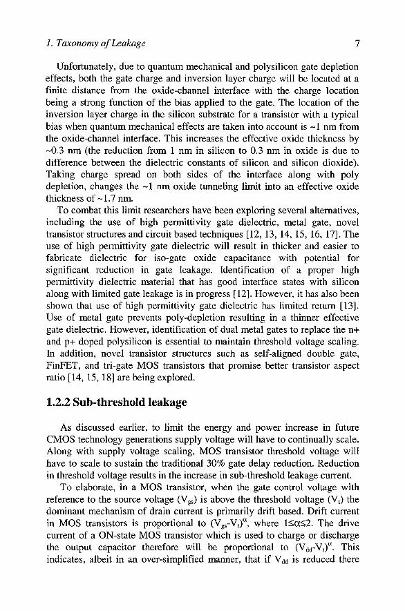
Unfortunately, due to quantum mechanical and polysilicon gate depletion effects, both the gate charge and inversion layer charge will be located at a finite distance from the oxide-channel interface with the charge location being a strong function of the bias applied to the gate. The location of the inversion layer charge in the silicon substrate for a transistor with a typical bias when quantum mechanical effects are taken into account is ~1 nm from the oxide-channel interface. This increases the effective oxide thickness by -0.3 nm (the reduction from 1 nm in silicon to 0.3 nm in oxide is due to difference between the dielectric constants of silicon and silicon dioxide). Taking charge spread on both sides of the interface along with poly depletion, changes the ~1 nm oxide tunneling limit into an effective oxide thickness of --1.7 nm.
To combat this limit researchers have been exploring several alternatives, including the use of high permittivity gate dielectric, metal gate, novel transistor structures and circuit based techniques [12, 13, 14, 15, 16, 17]. The use of high permittivity gate dielectric will result in thicker and easier to fabricate dielectric for iso-gate oxide capacitance with potential for significant reduction in gate leakage. Identification of a proper high permittivity dielectric material that has good interface states with silicon along with limited gate leakage is in progress [12]. However, it has also been shown that use of high permittivity gate dielectric has limited return [13]. Use of metal gate prevents poly-depletion resulting in a thinner effective gate dielectric. However, identification of dual metal gates to replace the n+ and p+ doped polysilicon is essential to maintain threshold voltage scaling. In addition, novel transistor structures such as self-aligned double gate, FinFET, and tri-gate MOS transistors that promise better transistor aspect ratio [14, 15, 18] are being explored.
1.2.2 Sub-threshold leakage
As discussed earlier, to limit the energy and power increase in future CMOS technology generations supply voltage will have to continually scale. Along with supply voltage scaling, MOS transistor threshold voltage will have to scale to sustain the traditional 30% gate delay reduction. Reduction in threshold voltage results in the increase in sub-threshold leakage current.
To elaborate, in a MOS transistor, when the gate control voltage with reference to the source voltage (Vgs) is above the threshold voltage (Vt) the dominant mechanism of drain current is primarily drift based. Drift current in MOS transistors is proportional to (Vgs-Vt)", where l<a<2. The drive current of a ON-state MOS transistor which is used to charge or discharge the output capacitor therefore will be proportional to (Vdd-Vt)". This indicates, albeit in an over-simplified manner, that if Vdd is reduced there

8 Leakage in Nanometer CMOS Technologies
needs to be a corresponding reduction in Vj to maintain the drive current. Now, as the transistor approaches the OFF-state, the Vgs goes below Vf Under this condition the drain current mechanism becomes predominantly diffusion based. Diffusion current, like bipolar transistors, depends exponentially on its control voltage. In other words the drain current changes exponentially with Vgs for Vgs below Vf Figure 1-6 illustrates how reduction in Vt therefore results in larger sub-threshold leakage current. In the illustration, for a sub-threshold swing (S) of 85mV/decade, the sub-threshold leakage current (IOFF) will increase by lOX if the Vt is reduced by 85mV.
c o
3 O c "i o
1 0.8 0.6 0.4 0.2
0
1 0.1
0.01 0.001
0.0001 0.00001
0.000001
0 0.5 1 1.5
Gate voltage
Figure 1-6: Relationship between threshold voltage (Vt) and sub-threshold leakage current (IQFF) for NMOS transistor. Assumes that the source terminal voltage was OV, so the gate voltage is same as Vgs.
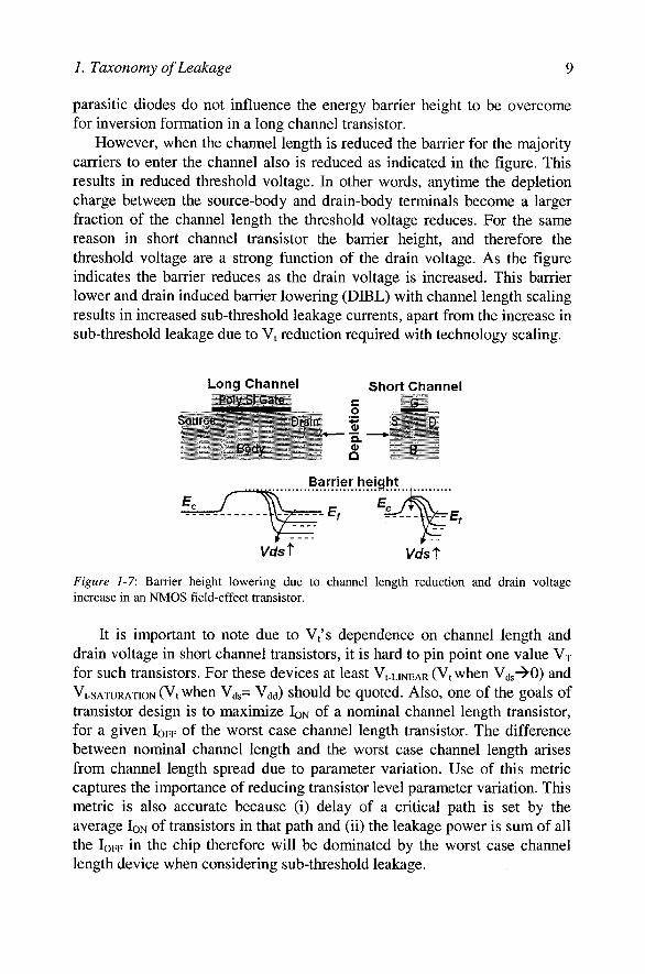
Additionally, with technology scaling, the MOS transistor channel length is reduced. As the channel length approaches the source-body and drain-body depletion widths, the charge in the channel due to these parasitic diodes become comparable to the depletion charge due to the MOS gate-body voltage [11], rendering the gate and body terminals to be less effective.
Figure 1-7 shows cross-sectional schematic of long channel and short channel transistors and their corresponding band conduction bands. The band diagram indicates the barrier that majority carriers in the source terminal have to overcome to enter the channel. In a given technology generation, since the source-body and drain-body depletion widths are predefined based on the dopings, the rate at which the barrier height increases as a function of distance from the source into the channel is constant. As the band diagram illustrates in Figure 1-7, the finite depletion width of the
1. Taxonomy of Leakage 9
parasitic diodes do not influence the energy barrier height to be overcome for inversion formation in a long channel transistor.
However, when the channel length is reduced the barrier for the majority carriers to enter the channel also is reduced as indicated in the figure. This results in reduced threshold voltage. In other words, anytime the depletion charge between the source-body and drain-body terminals become a larger fraction of the channel length the threshold voltage reduces. For the same reason in short channel transistor the barrier height, and therefore the threshold voltage are a strong function of the drain voltage. As the figure indicates the barrier reduces as the drain voltage is increased. This barrier lower and drain induced barrier lowering (DIBL) with channel length scaling results in increased sub-threshold leakage currents, apart from the increase in sub-threshold leakage due to Vt reduction required with technology scaling.
Long Channel short Channel Poly.Si Gate c Q
Source ^ ,̂ Drain "-g S , .D
Body I" B
^^^^^ Barrier height
vast vdst
Figure 1-7: Barrier height lowering due to channel length reduction and drain voltage increase in an NMOS field-effect transistor.
It is important to note due to Vt's dependence on channel length and drain voltage in short channel transistors, it is hard to pin point one value VT for such transistors. For these devices at least VI-LINEAR (Vt when Vds"^0) and
-SATURATION (Vt whcu Vds= V d̂) should be quoted. Also, one of the goals of transistor design is to maximize IQN of a nominal channel length transistor, for a given IQFF of the worst case channel length transistor. The difference between nominal channel length and the worst case channel length arises from channel length spread due to parameter variation. Use of this metric captures the importance of reducing transistor level parameter variation. This metric is also accurate because (i) delay of a critical path is set by the average IQN of transistors in that path and (ii) the leakage power is sum of all the loFF in the chip therefore will be dominated by the worst case channel length device when considering sub-threshold leakage.

10 Leakage in Nanometer CMOS Technologies
1,2.3 Junction tunneling leakage
To combat the sub-threshold leakage increase due to barrier reduction we need a MOS transistor with good aspect ratio. The challenge of dramatic increase in gate direct tunneling leakage with oxide thickness scaling limits was mentioned in Section 1.2.1. Scaling of junction depth to maintain the aspect ratio, in scaled transistors, leads to increase in the transistor series resistance. Therefore this limits how far the junction depth can be reduced. With channel length reduction, it is therefore necessary to increase the channel doping near the source-to-body and drain-to-body junctions to minimize the effect of barrier lowering. This increased doping in the channel edge is sometimes referred to as halo doping.
As the doping near these junctions are increased with scaling, junction tunneling leakage in the channel edge becomes more prevalent due to the emergence of n+ to p+ junctions. It is well known that reverse biased junctions that have heavy dopings on both side results in direct tunneling across these junctions. Furthermore with reducing volume of the transistors the metal silicide being used for source, gate, and drain terminals increase the probability of creating traps in the nearby heavily doped junctions, further increasing the junction tunneling. Raised source and terminals will help minimize this effect since the silicide distance to the junction is increased.
Ig leakage @ 30nm
1E-06
1E-07
1E-08
1.1 E-09 ill
— 1E-10
1E-11
1E-12
off leakage @ 30nm
iOiim
10 15 20
Doping Concentration (lO/cm^)
Figure 1-8: Junction edge leakage vs. doping concentration. Circles - data, squares -extrapolated points. Other sources of leakage at 30 nm have been added to the graph. [19]
Figure 1-8 shows the junction edge leakage (IJE) as a function of substrate doping at 25°C and IV reverse bias. Although the leakages are high (above InA/um at 30 nm channel length), they are still a lot less than sub-threshold and gate leakages at 30 nm. For the shorter channel transistors, extrapolating to the 10 nm gate lengths, and assuming a 1.6X doping concentration

1. Taxonomy of Leakage 11
increase per technology generation, the junction leakage approaches luA/um. Note that the data does not comprehend the impact of trap assisted increase injunction leakage.
It is worth noting that one of the scaling limits for the traditional MOS transistor structure arises from the fact that the depletion thicknesses of the drain-to-body and source-to-body junctions are finite. Therefore, there is a minimum channel length below which these junctions will short each other, resulting in direct drain-to-source tunneling. This is predicted to the fundamental limiter for scaling of the traditional MOS transistor structure [20].
1.3 IMPACT
It should be evident by now that in a given technology there is a trade-off between the three leakage sources. Increase in sub-threshold leakage current due to reduction in aspect ratio can be combated by reducing the oxide thickness and/or by increasing the channel doping near the junction - these will result in increase of one or both tunneling leakage currents.
Since different circuit styles may use different types of transistors, the relative importance of the leakage and therefore the optimization of the transistor parameters for each of these transistors may differ. For example, in SRAM circuits compared to logic circuits, it is customary to use longer channel length transistor to minimize impact of random dopant variations. Therefore, SRAM circuits maybe dominated by gate leakage, while logic transistors will be dominated by sub-threshold leakage. Similarly decoupling capacitors that are used to filter power supply noise are long channel MOS transistors. Therefore these transistors will suffer from increase in gate leakage, while sub-threshold and junction leakages have virtually no impact on such decoupling capacitors.
30 40 50 60 70
Temp (C)
90 100
Figure 1-9: Temperature dependence of sub-threshold leakage current per unit um transistor width, under the generational lengths of 0.18 um to 0.05 um.

12 Leakage in Nanometer CMOS Technologies
Sub-threshold leakage current in scaled technologies depends exponentially on temperature (Figure 1-9) since it is a diffusion mode of transport, while the tunneling currents have very weak temperature dependence. So, any temperature variation will significantly affect the subthreshold leakage current. All leakages components discussed in this section have strong direct exponential dependence on the supply voltage. So any voltage variations will affect the leakage current consumed. Also, more recently the electric field across critical dimensions such as oxide thickness have be increasing for high-performance designs, since thinner oxide are more reliable and can support higher fields. This has resulted in slow down on supply voltage scaling to push the performance envelope. This further aggravates the various leakage current components in high-performance design.
Furthermore, leakage current's strong environmental parameter (voltage, temperature, and process comer) dependencies make the power estimation of such a CMOS system complex. For example, the leakage power consumed by MOS circuit block in active state where the temperature will be higher will be very different from the same circuit in idle state. Note that a nearby circuit block's active state temperature will influence the idle state leakage of another block. The power consumed by a part in bum-in testing, where the temperature and voltage conditions are higher than normal operation, will strongly depend on the leakage sources and their sensitivity to temperature and voltage.
2-2
O (0
G> > c
0.18 0.36 0.72
L(^m)
Figure 1-10: Dependence of threshold voltage variation on channel length and drain voltage in 0.18 um channel length generation; n is the number of MOS transistor samples measured.
Additionally, transistor threshold voltage and therefore the sub-threshold leakage power have a strong dependence on the channel length, due the prior explained barrier lowering effects (Figure 1-10). So the power consumed by a circuit block will depend on the variations in the channel lengths of the constituent transistors of that circuit block. With scaling due to

1. Taxonomy of Leakage 13
improvements in lithography techniques channel length scaUng has been more aggressive compared to the ability to reduce oxide thickness and junction depth. This results in worse transistor aspect ratio and barrier lower effects with scaling, leading to increase sub-threshold leakage power dependence on channel length.
1.4 SOLUTIONS
The above mentioned leakage sources and their dependencies on environmental parameters make the impact of the leakage sources at the circuit and system levels quite intricate and diverse. Therefore, there is no one solution that will transcend all the negative effects of the transistor leakage sources.
The solution space spans the transistor, circuit, and system levels. They can be further divided in to (i) reduction and adaptation techniques that directly help minimize the impact of leakage and parameter variation, (ii) prediction methodologies that help understand the source and nature of its impact, and (iii) and administration method that help implement and manage an array of solutions.
1.4.1 Reduction and adaptation
The rest of the book will deal with explaining different reduction and adaptation techniques. In Chapter 2, the use of input vectors to minimize the idle leakage of a circuit block with virtually no performance impact is covered. In Chapters 3 and 4, power gating techniques and methodologies are explained. It is worth noting that power gating techniques help address all components of power consumption when a circuit block or a chip is in idle mode, at the expense of some degradation in circuit performance. Chapter 3 covers dynamic voltage scaling based power reduction as well. In Chapter 5 substrate biasing technique that allows electrical modulation of transistor threshold voltage is explained and its usage for power reduction is presented. Chapter 6 covers various adaptive design techniques to minimize impact of parameter variation on power consumption and design margins. Chapter 7 covers memory leakage reduction techniques.
There are two types of leakage power that is of importance (i) active leakage power and (ii) standby leakage power. Active leakage power is defined leakage power consumed by a nanoscale CMOS system when it doing useful work and standby leakage power is consumed when the system is idle. Chapter 8 focuses attention on extending traditionally standby or idle

14 Leakage in Nanometer CMOS Technologies
leakage reduction techniques for active leakage reduction. Also, uses of multi-performance transistors for power reduction are described in Chapter 8. Chapter 9 covers impact of leakage and parameter variation on testing. Chapter 12 introduces transistor design in technologies that are dominated by leakage.
1.4.2 Prediction
The present scaling trends have lead to leakage power being as much as 40% of the total power in the 90 nm generation [21]. Under this scenario, it is not only important to be able to reduce leakage power, but also to be able to predict leakage power more accurately. In this section we highlight the importance of including parameter variation in predicting leakage power accurately. Failure to do so will result in gross underestimation or overestimation, both of which are unacceptable.
Due to the wide variation expected in threshold voltage of MOS transistors from die-to-die and within-die during the life time of a process, present leakage current estimation techniques provide lower and upper bounds on the leakage current. The upper and lower bounds are at least an order of magnitude apart and leakage power of most chips lies between the two bounds as shown in [22]. In older technology generations, basing system design on the two leakage current bounds was acceptable since leakage power was a negligible component of the total power. In most systems, the worst case bound is assumed for the design. In technology generations where as much as half of the system power during active mode can be due to leakage, using the worse case bound estimation technique will lead to extremely pessimistic and expensive design solutions. One cannot base the system design on the lower bound since it will lead to overly optimistic and unreliable design solutions. Therefore, it will be crucial to estimate leakage current as accurately as possible. The upper and lower bound estimate equations and measurements are provided in the next part of this section.
The lower bound leakage current estimation of a chip is given as follows,
7 P_ JO *^n JO heak-l ~ U ^P "^ U ^n
where, Wp and w„ are the total PMOS and NMOS transistor widths in the chip; kp and kn are factors that determine percentage of PMOS and NMOS transistor widths that are in off state; fp and fn are the expected mean leakage currents per unit width of PMOS and NMOS transistors in a particular chip. The mean leakage current is obtained for transistors with mean threshold voltage or channel length. The upper bound leakage current estimation of a chip is related to the transistor leakage as follows.

7. Taxonomy of Leakage 15
T P_T^^ n J 3a ^leak-u ^ ^off-p + ^ ^c#-n
P /I
where, I^^off-p and /̂ t̂#-̂ z are the worst-case leakage current per unit width of PMOS and NMOS transistors. The worst-case leakage current is obtained for transistors with threshold voltage or channel length 5 cr lower than the mean leakage currents per unit width of PMOS and NMOS transistors in a particular chip.
To include the impact of within-die threshold voltage or channel length variation it is necessary to consider the entire range of leakage currents, not just the mean leakage or the worst-case leakage. Let us assume that the within-die threshold voltage or channel length variation follows a normal distribution with respect to transistor width, with ju being the mean and a being the sigma of the distribution. Let f be the leakage of the transistor with the mean threshold voltage or channel length. Then by performing the weighted sum of transistors of different leakage, we can estimate the total leakage of the chip. This is achieved by integrating the threshold voltage or channel length distribution multiplied by the leakage, as shown below.
-(^-M)^ (ju-x) I^W 1 ^^^ 2
heak =- T= \ e ^^ e ^ dx
In the above equation, the first exponent estimates the fraction of the total width for the transistor leakage estimated by the second exponent. If the distribution considered within-die is threshold voltage variation then x in the above equation represents threshold voltage and a will be equal to n(/>t [7]. If the distribution considered is channel length then x in the above equation will represent channel length and a will be equal to A. A can be estimated for a technology by measuring the relationship between channel length and transistor leakage. In the rest of this section, we will assume that the distribution of interest is the channel length, since this parameter is used to characterize a technology. Using error function properties, we can simplify the above equation to estimate the leakage of a chip that has both PMOS and NMOS transistors including within-die variation as follows [23],
kp
V /V +
-„^ , 2 ^ 2
where, Wp and w„ are the total PMOS and NMOS transistor widths in the chip; kp and kn are factors that determine percentage of PMOS and NMOS transistor widths that are in off state; fp and /̂ „ are the expected mean
16 Leakage in Nanometer CMOS Technologies
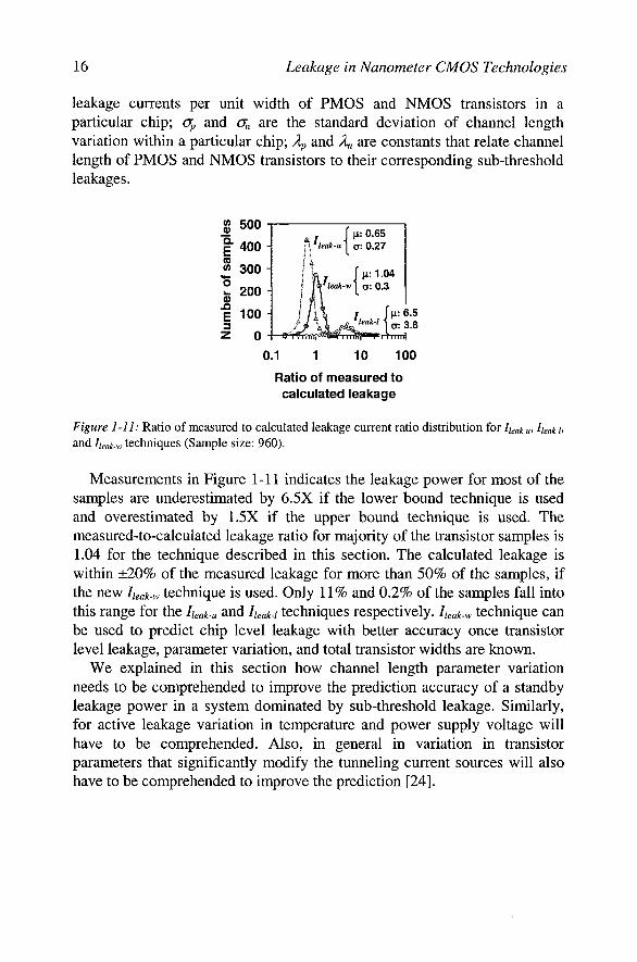
leakage currents per unit width of PMOS and NMOS transistors in a particular chip; Gp and <j„ are the standard deviation of channel length variation within a particular chip; Ap and Xn are constants that relate channel length of PMOS and NMOS transistors to their corresponding sub-threshold leakages.
0.1 10 100
Ratio of measured to calculated leakage
Figure 1-11: Ratio of measured to calculated leakage current ratio distribution for lieak-m heak-b and lieak-w techniques (Sample size: 960).
Measurements in Figure 1-11 indicates the leakage power for most of the samples are underestimated by 6.5X if the lower bound technique is used and overestimated by 1.5X if the upper bound technique is used. The measured-to-calculated leakage ratio for majority of the transistor samples is 1.04 for the technique described in this section. The calculated leakage is within ±20% of the measured leakage for more than 50% of the samples, if the new heak-w technique is used. Only 11% and 0.2% of the samples fall into this range for the lieak-u and lieak-i techniques respectively, luak-w technique can be used to predict chip level leakage with better accuracy once transistor level leakage, parameter variation, and total transistor widths are known.
We explained in this section how channel length parameter variation needs to be comprehended to improve the prediction accuracy of a standby leakage power in a system dominated by sub-threshold leakage. Similarly, for active leakage variation in temperature and power supply voltage will have to be comprehended. Also, in general in variation in transistor parameters that significantly modify the tunneling current sources will also have to be comprehended to improve the prediction [24].
1. Taxonomy of Leakage
1.4.3 Administration
17
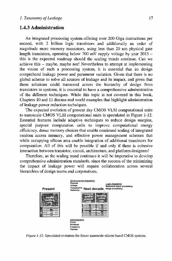
An integrated processing system offering over 200 Giga instructions per second, with 2 billion logic transistors and additionally an order of magnitude more memory transistors, using less than 20 nm physical gate length transistors, operating below 700 mV supply voltage by year 2015 -this is the expected roadmap should the scaling trends continue. Can we achieve this - maybe, maybe not! Nevertheless to attempt at implementing the vision of such a processing system, it is essential that its design comprehend leakage power and parameter variation. Given that there is no global scheme to solve all sources of leakage and its impact, and given that these solutions could transcend across the hierarchy of design from transistors to systems, it is essential to have a comprehensive administration of the different techniques. While this topic is not covered in this book. Chapters 10 and 11 discuss real world examples that highlight administration of leakage power reduction techniques.
The expected evolution of present day CMOS VLSI computational units to nanoscale CMOS VLSI computational units is speculated in Figure 1-12. Essential features include adaptive techniques to reduce design margins, special purpose computation units to improve computational energy efficiency, dense memory choices that enable continued scaling of integrated random access memory, and effective power management schemes that while occupying silicon area enable integration of additional transistors for computation. All of this will be possible if and only if there is cohesive interaction between transistor, circuit, architecture, and platform designers!
Therefore, as the scaling trend continues it will be imperative to develop comprehensive administration standards, since the success of the minimizing the impact of leakage power will require collaboration across several hierarchies of design teams and corporations.
Present
. units - I
Environmental Adaptation
' * " ^ * * ' Loah Adaptation Voltage Baseband signal processing
ReSSm?'"' Next decade tniage processing
p Adaptive 1 ^ ' t genetal- JReconfiB-j purposB 1 "raj»l9.
1 1 Itl
1 L I li
• • . -^•••C
' •• •
1 —-i-'-i-e ' " " 3 " ^ 1—1 : a
Administration Power Workload Frequency Thermal
Figure 1-12: Speculated evolution for future nanoscale silicon based CMOS systems.

18 Leakage in Nanometer CMOS Technologies
REFERENCES
[I] G.E. Moore, "Cramming more components onto integrated circuits," Electronics, vol. 38, no. 8, April 19, 1965.
[2] R. Smolan and J. Erwitt, One Digital Day - How the Microchip is Changing Our World, Random House, 1998.
[3] V. De and S. Borkar, "Technology and Design Challenges for Low Power & High Performance," Intl. Symp. Low Power Electronics and Design, pp. 163-168, Aug. 1999.
[4] K.G. Kempf, "Improving Throughput across the Factory Life-Cycle," Intel Technology Journal, Q4, 1998.
[5] A. Chandrakasan, S. Sheng, and R. W. Brodersen, "Low-Power CMOS Digital design," IEEE J, Solid-State Circuits, vol. 27, pp. 473-484, Apr. 1992.
[6] S. Thompson, P. Packan, and M. Bohr, "MOS Scaling: Transistor Challenges for the list CQntury,'' Intel Technology Journal, Q3, 1998.
[7] Y. Taur and T. H. Ning, Fundamentals of Modern VLSI Transistors, Cambridge University Press, 1998
[8] D. Antoniadis and J.E. Chung, "Physics and Technology of Ultra Short Channel MOSFET Transistors," Intl. Electron transistors Meeting, pp. 21-24, 1991.
[9] D.A. MuUer, T. Sorsch, S. Moccio, F.H. Baumann, K. Evans-Lutterodt, and G. Timp, "The Electronic Structure at the Atomic Scale of Ultrathin Gate Oxides," Nature, vol. 399, pp. 758-761, June 1999.
[10] M. Schulz, "The End of the Road for Silicon," Nature, vol. 399, pp. 729-730, June 1999.
[II] S.-H.Lo, D.A. Buchanan, Y. Taur, and W. Wang, IEEE Electron Transistor Letter, 1997, p. 209.
[12] C. H. Lee, S. J. Lee, T. S. Jeon, W. P. Bai, Y. Sensaki, D. Roberts, and D. L. Kwong, "Ultra Thin ZrO(2) and Zr(27)Si( 10)0(63) Gate Dielectrics Directly Prepared on Si-Substrate by Rapid Thermal Processing," SRC Techcon, pp. 46, Sep. 2000.
[13] N. R. Mohapatra, M. P. Desai, S. Narendra, and V. R. Rao, "The effect of high-K gate dielectrics on deep submicrometer CMOS transistor and circuit performance," IEEE Transactions on Electron Transistors, vol. 49, pp. 826-831, May 2002.
[14] J. Lee, G. Tarachi, A. Wei, T. A. Langdo, E. A. Fitzgerald, D. Antoniadis, "Super self-aligned double-gate (SSDG) MOSFETs utilizing oxidation rate difference and selective epitaxy," Intl. Electron Transistors Meeting, pp. 71-74, 1999.
[15] R. Chau, B. Boyanov, B. Doyle, M. Doczy, S. Datta, S. Hareland, B. Jin, J. Kavalieros, M. Metz, "Silicon nano-transistors for logic applications," Physica E, Low-dimensional Systems andNanostructures, Vol. 19, Issues 1-2, pp. 1-5, July 2003.
[16] I. Kohno, T. Sano, N. Katoh, and K. Yano, "Threshold Canceling Logic (TCL): A Post-CMOS Logic Family Scalable Down to 0.02 mm," Intl. Solid-State Circuits Conf., pp. 218-219,2000.
[17] T. Kuroda, T. Fujita, S, Mita, T. Nagamatsu, S. Yoshioka, K. Suzuki, F. Sano, M, Norishima, M. Murota, M. Kako, M. Kinugawa, M. Kakumu, and T. Sakurai, "A 0.9-V, 150-MHz, 10-mW, 4-mm2, 2-D Discrete Cosine Transform core Processor with Variable Threshold-Voltage (VT) Scheme," IEEE J. Solid-State Circuits, vol. 31, pp. 1770-1779, Nov. 1996.
[18] X. Huang, W-C. Lee, C. Kuo, D. Hisamoto, L. Chang, J. Kedzierski, E. Anderson, H. Takeuchi, Y-K. Choi, K. Asano, V. Subramanian, T-J. King, J. Bokor, C. Hu, "Sub 50-nm FinFET: PMOS," lEDM Technical Digest, Washington, DC, pp. 67-70, December 5-8, 1999.
[19] Doyle, B., Arghavani, R., Barlage, D., Datta, S., Doczy, M., Kavalieros, J., Murthy, A., and Chau, R., "Transistor Elements for 30nm Physical Gate Lengths and Beyond." Intel

1. Taxonomy of Leakage 19
Technology Journal, http://developer.intel.com/technology/itj/2002/volume06issue02/ (May 2002).
[20] B. Hoeneisen, and C.A. Mead, "Fundamental Limitations in Microelectronics I: MOS Technology," Solid-State Electronics, vol. 15, pp. 819-829, July 1972.
[21] A. Grove, http://www.intel.com/pressroom/archive/speeches/grove_ 20021210.pdf, lEDM 2002 Keynote Luncheon Speech.
[22] A. Keshavarzi, S. Ma, S. Narendra, B. Bloechel, K. Mistry, T. Ghani, S. Borkar, and V. De, "Effectiveness of reverse body bias for leakage control, in scaled dual Vt CMOS ICs," Intl. Symp. Low Power Electronics and Design, pp. 207-212, Aug. 2001.
[23] S. Narendra, V. De, S. Borkar, D. Antoniadis, and A. Chandrakasan, "Full-chip subthreshold leakage power prediction and reduction techniques for sub-0.18-um CMOS," IEEE Journal of Solid-State Circuits, vol. 39, pp. 501-510, Sept. 2004.
[24] Dongwoo Lee, Wesley Kwong, David Blaauw, Dennis Sylvester, "Analysis and Minimization Techniques for Total Leakage Considering Gate Oxide Leakage," ACM/IEEE Design Automation Conference (DAC), pp. 175-186, June 2003.

Chapter 2
LEAKAGE DEPENDENCE ON INPUT VECTOR
Siva Narendra^ Yibin Ye''̂ , Shekar Borkar^, Vivek De''̂ , and Anantha Chandrakasan* ^Tyfone, Inc., USA, ̂ Intel Corp., USA, and "^Massachusetts Institute of Technology, USA
2.1 INTRODUCTION
As described earlier to limit the energy and power increase in future CMOS technology generations, the supply voltage (Vdd) will have to continually scale. The amount of energy reduction depends on the magnitude of Vdd scaling. Along with Vdd scaling, the threshold voltage (Vt) of MOS transistors will have to scale to sustain the traditional 30% gate delay reduction. These Vdd and Vt scaling requirements pose several technology and circuit design challenges. In this chapter the term leakage refers to subthreshold leakage, unless otherwise explicitly mentioned.
One of challenge with technology scaling is the rapid increase in subthreshold leakage power due to Vt reduction. Should the present scaling trend continue it is expected that the sub-threshold leakage power will become a considerable constituent of the total dissipated power. In such a system it becomes crucial to identify techniques to reduce this leakage power component. It has been shown previously that the stacking of two off transistors has significantly reduced sub-threshold leakage compared to a single off transistor. The stack effect can therefore be used not jus for leakage reduction by forcing stacks, but also using natural stacks that existing in logic gates. Natural stacks can be realized by loading an appropriate primary input vector such that it propagates to maximize the total channel width of stacked transistors that are OFF,
In this chapter we present a model that predicts the stack effect factor, which is defined as the ratio of the leakage current in one off transistor to the leakage current in a stack of two off transistors [1]. Model derivation based on transistor fundamentals and verification of the model through statistical