lecture 12 - university of california, berkeleyee290d/fa13/lecturenotes/...lecture 12 •...
TRANSCRIPT

Lecture 12• Process-induced Variations II:
Systematic– Lithographic Proximity Effect– Layout Dependent Strain– Well Proximity Effect
Reading: multiple research articles (reference list at the end of this lecture)
OPC

Lithography Proximity Effect (LPE)
11/6/2013 2
Nominal
Underexposed
Overexposed
NAND2 Delay Distributions
Defocus (nm)M
ean
Del
ay o
ver 3
00 s
ampl
es (p
s)Actual LayoutDesired 6T SRAM LayoutCourtesy of M. Rieger (Synopsys)
• Optical Proximity Correction (OPC)used to compensate for image errors due todiffraction effects by adding extra polygons tothe pattern on the photomask• Phase Shift Mask (PSM)used to reduce the light interference bychanging the thickness of transmitting patternson the photomask (i.e. creating a phase shiftlight)
These resolution enhancement techniqueshelp to reduce the pattern distortions, yetstill end with round corners.

Impact of Poly Corner Rounding: Gate-Extension Dependence
11/6/2013 3Nuo Xu EE 290D, Fall 2013
M. Choi, SPIE (2009)1st Gate Patterning 2nd Gate Patterning
Poly corner rounding can be improved by using multiple patterning/exposure techniques.

Impact of Active Region Rounding: Asymmetric Source/Drain
11/6/2013 4Nuo Xu EE 290D, Fall 2013
M. Choi, SPIE (2009)

STI Proximity Effect
11/6/2013 5Nuo Xu EE 290D, Fall 2013
• Due to the different thermal expansion coefficients between Si and STI, there exists biaxial compressive residual stress in the active region after processing.
• STI-stress generally increases PMOS current and decreases NMOS current.
• Stress relaxes exponentially with increased distance from Si/STI boundary.
R. A. Bianchi, IEDM (2002)

Layout Dependent Strain:eSiGe Source/Drain
11/6/2013 6Nuo Xu EE 290D, Fall 2013
V. Moroz, SISPAD (2008)
Isolated PMOS Nested PMOS Comparison of Stress

11/6/2013 7
N. Xu, TDMR (2011)
H. Aikawa, VLSI-T (2008)
Other Sources for Layout Dependent Strain
PMOS
Nuo Xu EE 290D, Fall 2013
Contact-induced Strain
sCESL-induced Strain
sCESL

Well Proximity Effect (WPE)
11/6/2013 8Nuo Xu EE 290D, Fall 2013
Illustration of WPE N-MOSFET VTH vs. WP
2-D WPE
NA
• During ion implantation, kineticions scatter back out of PR andbecome embedded in the Sinear PR edge, causing VTH shift.
• The affected distance is ~ 1um.• Small angle II helps, but never
avoids WPE.
T.B. Hook, T-ED (2003)

Another WPE: Stress-induced Enhanced/Retarded Diffusion
11/6/2013 9Nuo Xu EE 290D, Fall 2013
H. Tsuno, VLSI-T (2007)
N-MOSFET VTH Shift vs. Inverse of (l) STI-Gate Distance and (r)Gate Spacing

Design for Manufacturability (DFM)
11/6/2013 10Nuo Xu EE 290D, Fall 2013
Carrier Mobility Threshold Voltage
where
W
STIV
STIP
LPEDPS
SASB
W, L (dominant) DPS: dummy poly(gate)
spacing LPE: poly-extension (over
active region) length SA/B: active region length STIP/V: STI distance to
active region …
Compact modeling is the best solution to leverage between the accuracy and design complexity.

Monitors for Systematic Variability
11/6/2013 11Nuo Xu EE 290D, Fall 2013
45nm Si Test Chip
Defocus and LPE Vertial STIS & WPE
Ring oscillators (RO) and OFF-state transistors are often used to characterize transistors’ performance and leakage.
L. Wang & N. Xu, CICC (2010)

Summary of Systematic Variability on Planar Bulk MOSFETs
11/6/2013 12Nuo Xu EE 290D, Fall 2013
Courtesy of X.-W. Lin (Synopsys)
standard logic circuit performance shift w/ WPE
impacts of different systematic variability sources
Y.-M. Sheu, CICC (2005)
Layout-dependent strain and WPE play the dominant role on transistor performance’s drift.
Small active-region area cells suffer more from systematic variability.
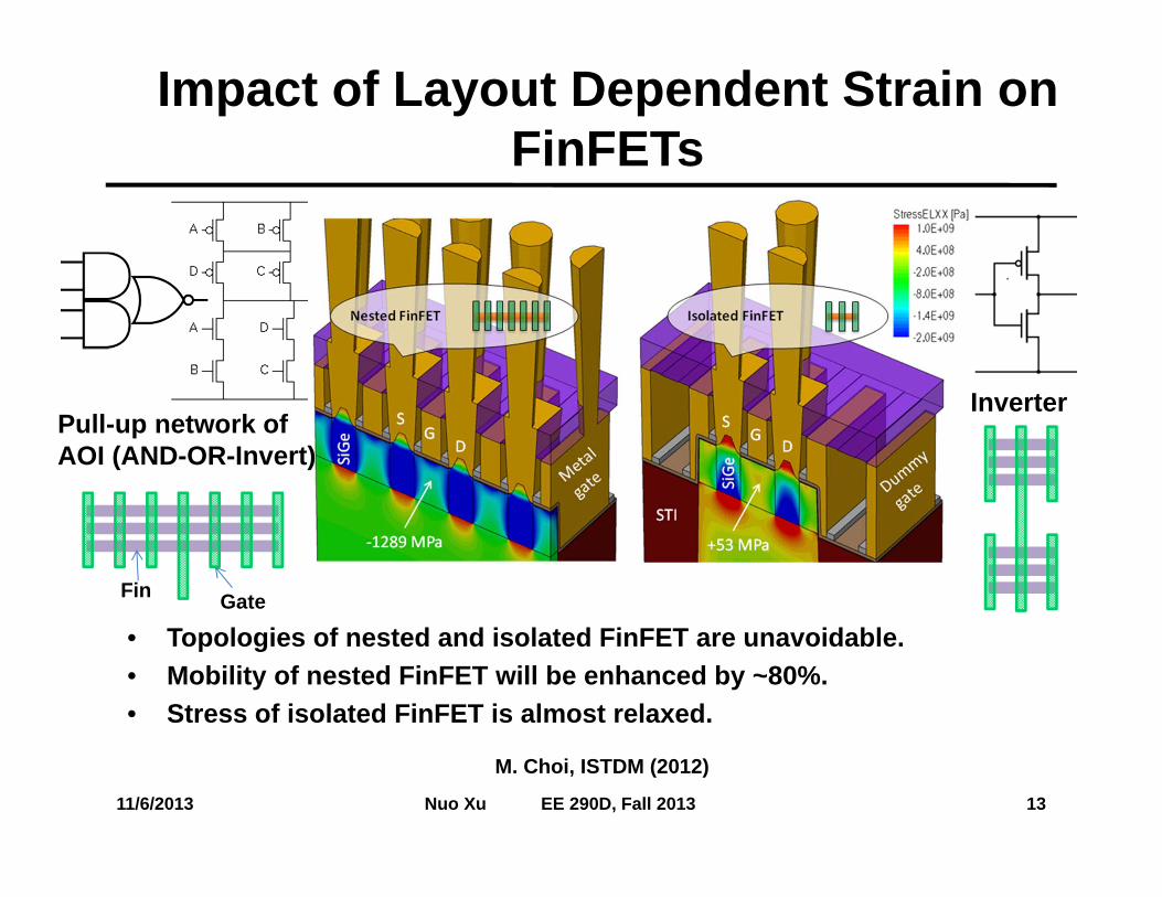
Impact of Layout Dependent Strain on FinFETs
Inverter
• Topologies of nested and isolated FinFET are unavoidable. • Mobility of nested FinFET will be enhanced by ~80%.• Stress of isolated FinFET is almost relaxed.
Pull-up network of AOI (AND-OR-Invert)
GateFin
11/6/2013 13Nuo Xu EE 290D, Fall 2013
M. Choi, ISTDM (2012)
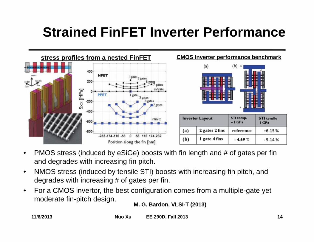
Strained FinFET Inverter Performance
11/6/2013 14Nuo Xu EE 290D, Fall 2013
M. G. Bardon, VLSI-T (2013)
CMOS Inverter performance benchmark
• PMOS stress (induced by eSiGe) boosts with fin length and # of gates per fin and degrades with increasing fin pitch.
• NMOS stress (induced by tensile STI) boosts with increasing fin pitch, and degrades with increasing # of gates per fin.
• For a CMOS invertor, the best configuration comes from a multiple-gate yet moderate fin-pitch design.
stress profiles from a nested FinFET

References1. T. B. Hook et al., “Lateral Ion Implant Straggle and Mask Proximity Effect,” IEEE Transactions on
Electron Devices, vol.50, no.9, pp. 1946-1951, 2003.2. R.A. Bianchi et al., “Accurate Modeling of Trench Isolation Induced Mechanical Stress Effects on
MOSFET Electrical Performance,” IEEE IEDM Tech. Dig., pp.117-120, 2002.3. V. Moroz et al., “The Impact of Layout on Stress-Enhanced Transistor Performance,” SISPAD
Tech. Dig., pp.143-146, 2005.4. N. Xu et al., “Physically based Modeling of Stress Induced Variation in Nanoscale Transistor
Performance,” IEEE Transactions on Device and Material Reliability, vol.11, no.3, pp. 378-386,2011.
5. H. Aikawa et al., “Variability Aware Modeling and Characterization in Standard Cell in 45nm CMOSwith Stress Enhancement Technique,” Symp. VLSI Tech., pp.90-91, 2008.
6. H. Tsuno et al., “Advanced Analysis and Modeling of MOSFET Characteristics Fluctuation Causedby Layout Variation,” Symp. VLSI Tech., pp.204-205, 2007.
7. L. T.-N. Wang et al., “Parameter-Specific Ring Oscillator for Process Monitoring at the 45nmNode,” IEEE CICC Tech. Dig., 2010.
8. Y.-M. Sheu et al., “Modeling Well Edge Proximity Effect on Highly-Scaled MOSFETs,” IEEE CICCTech. Dig., 2005.
9. M. Choi et al., “14nm FinFET Stress Engineering with Epitaxial SiGe Source/Drain,” InternationalSiGe Technology and Device Meeting, Berkeley, CA, 2012.
10. M. G. Bardon et al., “Layout induced Stress Effects in 14nm and 10nm FinFETs and their Impacton Performance,” Symp. VLSI Tech.Dig., pp. 114-115, 2013.