lecture 13: sequential circuits - school of computingrajeev/cs3810/slides/3810-13.pdf · lecture...
TRANSCRIPT

1
Lecture 13: Sequential Circuits
• Today’s topics:
� Carry-lookahead adder� Clocks and sequential circuits� Finite state machines
• Reminder: Assignment 5 due on Thursday 10/12,mid-term exam Tuesday 10/24

2
Speed of Ripple Carry
• The carry propagates thru every 1-bit box: each 1-bit box sequentiallyimplements AND and OR – total delay is the time to go through 64 gates!
• We’ve already seen that any logic equation can be expressed as thesum of products – so it should be possible to compute the result by going through only 2 gates!
• Caveat: need many parallel gates and each gate may have a verylarge number of inputs – it is difficult to efficiently build such large gates, so we’ll find a compromise:
� moderate number of gates
� moderate number of inputs to each gate
� moderate number of sequential gates traversed

3
Computing CarryOut
CarryIn1 = b0.CarryIn0 + a0.CarryIn0 + a0.b0CarryIn2 = b1.CarryIn1 + a1.CarryIn1 + a1.b1
= b1.b0.c0 + b1.a0.c0 + b1.a0.b0 +a1.b0.c0 + a1.a0.c0 + a1.a0.b0 + a1.b1
…CarryIn32 = a really large sum of really large products
• Potentially fast implementation as the result is computedby going thru just 2 levels of logic – unfortunately, eachgate is enormous and slow

4
Generate and Propagate
Equation re-phrased:ci+1 = ai.bi + ai.ci + bi.ci
= (ai.bi) + (ai + bi).ci
Stated verbally, the current pair of bits will generate a carryif they are both 1 and the current pair of bits will propagatea carry if either is 1
Generate signal = ai.biPropagate signal = ai + bi
Therefore, ci+1 = gi + pi . ci
5
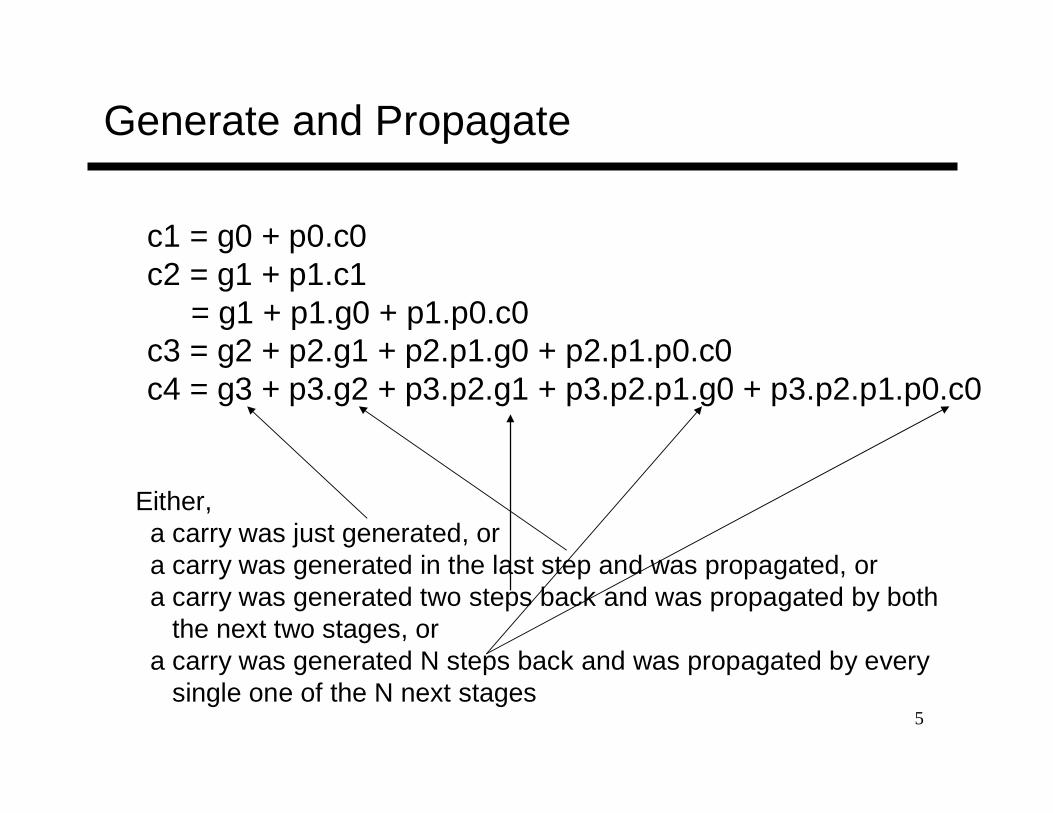
Generate and Propagate
c1 = g0 + p0.c0c2 = g1 + p1.c1
= g1 + p1.g0 + p1.p0.c0c3 = g2 + p2.g1 + p2.p1.g0 + p2.p1.p0.c0c4 = g3 + p3.g2 + p3.p2.g1 + p3.p2.p1.g0 + p3.p2.p1.p0.c0
Either, a carry was just generated, ora carry was generated in the last step and was propagated, ora carry was generated two steps back and was propagated by both
the next two stages, ora carry was generated N steps back and was propagated by every
single one of the N next stages

6
Divide and Conquer
• The equations on the previous slide are still difficult to implement aslogic functions – for the 32nd bit, we must AND every single propagatebit to determine what becomes of c0 (among other things)
• Hence, the bits are broken into groups (of 4) and each group computes its group-generate and group-propagate
• For example, to add 32 numbers, you can partition the task as a tree
.. . . .
. . . . . . . . . . . . . . . .

7
P and G for 4-bit Blocks
• Compute P0 and G0 (super-propagate and super-generate) for thefirst group of 4 bits (and similarly for other groups of 4 bits)P0 = p0.p1.p2.p3G0 = g3 + g2.p3 + g1.p2.p3 + g0.p1.p2.p3
• Carry out of the first group of 4 bits isC1 = G0 + P0.c0C2 = G1 + P1.G0 + P1.P0.c0…
• By having a tree of sub-computations, each AND, OR gate has fewinputs and logic signals have to travel through a modest set ofgates (equal to the height of the tree)

8
Example
Add A 0001 1010 0011 0011and B 1110 0101 1110 1011
g 0000 0000 0010 0011p 1111 1111 1111 1011
P 1 1 1 0G 0 0 1 0
C4 = 1

9
Carry Look-Ahead Adder
• 16-bit Ripple-carrytakes 32 steps
• This design takeshow many steps?

10
Clocks
• A microprocessor is composed of many different circuitsthat are operating simultaneously – if each circuit X takes ininputs at time TIX, takes time TEX to execute the logic,and produces outputs at time TOX, imagine thecomplications in co-ordinating the tasks of every circuit
• A major school of thought (used in most processors builttoday): all circuits on the chip share a clock signal (asquare wave) that tells every circuit when to acceptinputs, how much time they have to execute the logic, andwhen they must produce outputs

11
Clock Terminology
Cycle time
Rising clock edge
Falling clock edge
4 GHz = clock speed = 1 = 1 .cycle time 250 ps

12
Sequential Circuits
• Until now, circuits were combinational – when inputs change, theoutputs change after a while (time = logic delay thru circuit)
CombinationalCircuit
Inputs Outputs
• We want the clock to act like a start and stop signal – a “latch” isa storage device that stores its inputs at a rising clock edge andthis storage will not change until the next rising clock edge
CombinationalCircuit
Outputs
CombinationalCircuit
CombinationalCircuit
Latch Latch
Inputs
Clock Clock

13
Sequential Circuits
• Sequential circuit: consistsof combinational circuit anda storage element
• At the start of the clockcycle, the rising edgecauses the “state” storageto store some input values
• This state will not change for an entire cycle (until next rising edge)
• The combinational circuit has some time to accept the valueof “state” and “inputs” and produce “outputs”
• Some of the outputs (for example, the value of next “state”) may feedback (but through the latch so they’re only seen in the next cycle
State
Combinational Cct
Clock
Inputs Outputs
Inputs

14
Designing a Latch
• An S-R latch: set-reset latch
� When Set is high, a 1 is stored
� When Reset is high, a 0 is stored
� When both are low, the previous state is preserved (hence,known as a storage or memory element)
� When both are high, the output is unstable – this set of inputsis therefore not allowed
Verify the above behavior!

15
D Latch
• Incorporates a clock
• The value of the input D signal (data) is stored only when the clockis high – the previous state is preserved when the clock is low

16
D Flip Flop
• Terminology:Latch: outputs can change any time the clock is high (asserted) Flip flop: outputs can change only on a clock edge
• Two D latches in series – ensures that a value is stored only onthe falling edge of the clock

17
Sequential Circuits
• We want the clock to act like a start and stop signal – a “latch” isa storage device that stores its inputs at a rising clock edge andthis storage will not change until the next rising clock edge
CombinationalCircuit
Outputs CombinationalCircuit
Latch Latch
Inputs
Clock Clock

18
Finite State Machine
• A sequential circuit is described by a variation of a truthtable – a finite state diagram (hence, the circuit is alsocalled a finite state machine)
• Note that state is updated only on a clock edge
Next-stateFunction
OutputFunction
CurrentStateClock
Inputs
Nextstate
Outputs

19
State Diagrams
• Each state is shown with a circle, labeled with the statevalue – the contents of the circle are the outputs
• An arc represents a transition to a different state, with theinputs indicated on the label
0 10 1D = 1
D = 0
D = 0 D = 1
This is a state diagram for ___?

20
3-Bit Counter
• Consider a circuit that stores a number and increments the value onevery clock edge – on reaching the largest value, it starts again from 0
Draw the state diagram:
� How many states?
� How many inputs?

21
3-Bit Counter
• Consider a circuit that stores a number and increments the value onevery clock edge – on reaching the largest value, it starts again from 0
Draw the state diagram:
� How many states?
� How many inputs?
000
000
001
001
010
010
011
011
100
100
101
101
110
110
111
111

22
Traffic Light Controller
• Problem description: A traffic light with only green and red; either theNorth-South road has green or the East-West road has green (bothcan’t be red); there are detectors on the roads to indicate if a car ison the road; the lights are updated every 30 seconds; a light needchange only if a car is waiting on the other road
State Transition Table:How many states?How many inputs?How many outputs?

23
State Transition Table
• Problem description: A traffic light with only green and red; either theNorth-South road has green or the East-West road has green (bothcan’t be red); there are detectors on the roads to indicate if a car ison the road; the lights are updated every 30 seconds; a light mustchange only if a car is waiting on the other road
State Transition Table:CurrState InputEW InputNS NextState=Output
N 0 0 NN 0 1 NN 1 0 EN 1 1 EE 0 0 EE 0 1 NE 1 0 EE 1 1 N

24
State Diagram
State Transition Table:CurrState InputEW InputNS NextState=Output
N 0 0 NN 0 1 NN 1 0 EN 1 1 EE 0 0 EE 0 1 NE 1 0 EE 1 1 N

25
Title
• Bullet