lecture 13 symbol timing synchronization · 2016-11-09 · lecture 13 symbol timing...
TRANSCRIPT

1
EE4900/EE6720 Digital Communications Suketu Naik
EE4900/EE6720: Digital Communications
Lecture 13
Symbol Timing
Synchronization

2
EE4900/EE6720 Digital Communications Suketu Naik
Block Diagrams of Communication System
Digital Communication System
Informatio
n (sound,
video, text,
data, …)
Transducer &
A/D ConverterModulator
Source
Encoder
Channel
Encoder
Tx RF
System
Output
Signal
D/A Converter
and/or output
transducer
DemodulatorSource
Decoder
Channel
Decoder
Rx RF
System
Channel

3
EE4900/EE6720 Digital Communications Suketu Naik
Symbol Timing Error can create,
1) Uncertainty: where is the
starting sample out
of the matched filter?
2) Scattered constellation points:
close to the decision boundaries
This can happen regardless of
Carrier Phase synchronization
and absence of noise
How to address the timing error?
Symbol Timing Synchronization: Estimating the receiver
clock that is aligned in both phase and frequency with the
transmitter clock
Problem: Where is the starting sample?
Scattered constellation points
due to symbol timing error
4
EE4900/EE6720 Digital Communications Suketu Naik
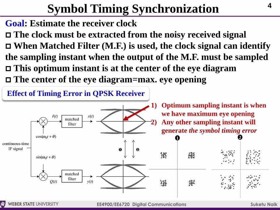
Symbol Timing SynchronizationGoal: Estimate the receiver clock
The clock must be extracted from the noisy received signal
When Matched Filter (M.F.) is used, the clock signal can identify
the sampling instant when the output of the M.F. must be sampled
This optimum instant is at the center of the eye diagram
The center of the eye diagram=max. eye opening
Effect of Timing Error in QPSK Receiver
1) Optimum sampling instant is when
we have maximum eye opening
2) Any other sampling instant will
generate the symbol timing error1 2

5
EE4900/EE6720 Digital Communications Suketu Naik
Continuous-time
M-ary PAM
6
EE4900/EE6720 Digital Communications Suketu Naik
Basic Problem Formulation
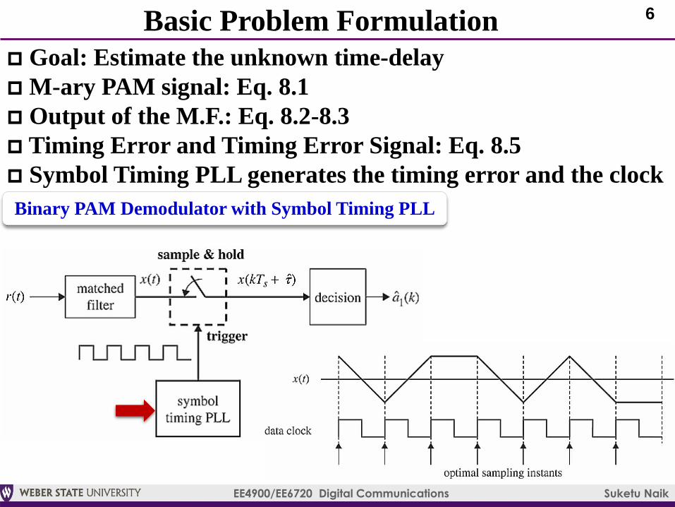
Goal: Estimate the unknown time-delay
M-ary PAM signal: Eq. 8.1
Output of the M.F.: Eq. 8.2-8.3
Timing Error and Timing Error Signal: Eq. 8.5
Symbol Timing PLL generates the timing error and the clock
Binary PAM Demodulator with Symbol Timing PLL
7
EE4900/EE6720 Digital Communications Suketu Naik
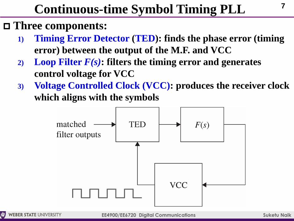
Continuous-time Symbol Timing PLL
Three components:1) Timing Error Detector (TED): finds the phase error (timing
error) between the output of the M.F. and VCC
2) Loop Filter F(s): filters the timing error and generates
control voltage for VCC
3) Voltage Controlled Clock (VCC): produces the receiver clock
which aligns with the symbols

8
EE4900/EE6720 Digital Communications Suketu Naik
Continuous-time Symbol Timing PLL
Comparison with generic PLL1) TED => Phase Detector
2) Loop Filter => Loop Filter
3) VCC => VCO
Symbol Timing PLL Generic PLL
Key component in the Symbol Timing PLL is the TED because it
must extract the embedded clock from the M.F. output

9
EE4900/EE6720 Digital Communications Suketu Naik
TED: How to generate the timing error
Eye Diagram
Optimum
sampling instant is
when we have
maximum eye
opening
Optimum sampling
instant is when slope of
the eye diagram = 0
Slope of the eye diagram
can be used to generate the
timing error
Note that the derivative of
the eye diagram shows:
1) zero to pos. or zero to neg.
transition
2) pos. to zero or neg. to zero
transition
This means symbol timing
PLL must have data sign
transitions (-1 to 1 or 1 to -1)

10
EE4900/EE6720 Digital Communications Suketu Naik
TED: How to generate the timing error
Sampling Instant is early,
Increase VCC clock period
Sampling Instant is late,
Decrease VCC clock period
-1 to +1
transition
+1 to -1
transition
Goal:
Slope=Zero
Sampling Instant is early,
Increase VCC clock period
+1 to -1
transition
-1 to +1
transition
Sampling Instant is late,
Decrease VCC clock period

11
EE4900/EE6720 Digital Communications Suketu Naik
Timing Error Signal for PAM
Timing error signal for the Decision-directed PLL: Eq. 8.7
Binary PAM symbol estimate: Eq. 8.8
Note that the error signal is zero (oval) when there are no data
transitions (repetitive symbols): this is addressed by randomizer at
Tx
Timing Error Signal
Data transitions are necessary
12
EE4900/EE6720 Digital Communications Suketu Naik
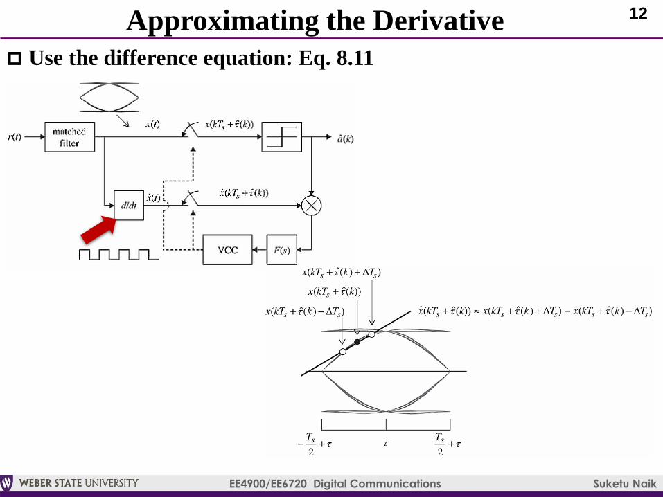
Approximating the Derivative
Use the difference equation: Eq. 8.11

13
EE4900/EE6720 Digital Communications Suketu Naik
Continuous-time
M-ary QAM

14
EE4900/EE6720 Digital Communications Suketu Naik
Continuous-time MQAM Symbol Timing
M-ary QAM signals: Eq. 8.13-8.14
Timing Error Signal: Eq. 8.18-8.20
QPSK Symbol
Timing PLL

15
EE4900/EE6720 Digital Communications Suketu Naik
Discrete-time
M-ary PAM

16
EE4900/EE6720 Digital Communications Suketu Naik
Discrete-time MPAM Symbol Timing
Goal: given symbols at a symbol rate and corresponding
sampling rate, one of the N samples is aligned
Generic MPAM Symbol Timing Sync
Sampling Rate Symbol Rate
Interpolator Output:
One of the N samples is aligned
Matched Filter Output:
No alignment

17
EE4900/EE6720 Digital Communications Suketu Naik
Discrete-time MPAM Symbol Timing
Discrete Symbol Timing PLL will move the samples at
the desired time instants: also known as interpolation
Interpolator must be adaptive to accommodate unknown
time delay τ
Sampling Rate Symbol Rate
Interpolator Output:
One of the N samples is alignedMatched Filter Output:
No alignment

18
EE4900/EE6720 Digital Communications Suketu Naik
Discrete-time PLL for Symbol Timing
Four Components:
Interpolator & Timing Error Detector (TED)=>PD
Loop Filter F(z) => Loop Filter F(z)
Interpolation Control => DDS
From
Matched
Filter
To Decision
Block

19
EE4900/EE6720 Digital Communications Suketu Naik
Discrete-time PLL for Symbol Timing
Timing Error Detector (TED)
Maximum Likelihood Timing Error Detector (MLTED)
Early-Late Timing Error Detector (ELTED)
Zero Crossing Timing Error Detector (ZCTED)
Gardner Timing Error Detector (GTED)
Mueller and Muller Timing Error Detector (MMTED)
From
Matched
Filter
To Decision
Block

20
EE4900/EE6720 Digital Communications Suketu Naik
Zero Crossing Timing Error Detector (ZCTED)
Goal: TED in general produces error signal once per
symbol
Eq. 8.24 where, Timing Error 𝝉𝒆 = 𝝉 − ො𝝉 TED will produce 𝝉𝒆 just as generic PLL produces
phase error
𝝉𝒆 a function of interpolated matched filter outputs
and the symbols (or their estimates)
ZCTED finds zero crossings in the eye diagram
ZCTED operates at 2 samples/symbol
ZCTED produces zero error at every other sample
aligned with zero crossing of the interpolated M.F. symbol
ZCTED produces other samples that are aligned with
the optimum sampling instant
ZCTED error signal (decision-directed PLL): Eq. 8.37

21
EE4900/EE6720 Digital Communications Suketu Naik
Zero Crossing Timing Error Detector (ZCTED)
Symbol
Estimate
Symbol
EstimateInterpolated M.F.
outputs at 2
samples/symbol)
Pos. Timing
Error: data
transition is
pos. to neg.
Neg. Timing
Error: data
transition is
neg. to pos.
Bin-PAM Symbol
Estimates: Eq. 8.38

22
EE4900/EE6720 Digital Communications Suketu Naik
ZCTED Example
From
Interpolator
Signum
Function
(Zero
Crossing
Threshold)
Fig. 8.4.25
To
Loop
Filter
From Interpolation
Control
Symbol
Estimate a(k)Symbol
Estimate
a(k-1)
2 Samples/Symbol

23
EE4900/EE6720 Digital Communications Suketu Naik
Discrete-time PLL for Symbol Timing
Four Components:
Interpolator & Timing Error Detector (TED)=>PD
Loop Filter F(z) => Loop Filter F(z)
Interpolation Control => DDS
From
Matched
Filter
To Decision
Block

24
EE4900/EE6720 Digital Communications Suketu Naik
Interpolation
Goal: Synchronize (or align) the symbol samples
to an optimum sampling instant
Q: How do we determine that?
A: By looking at the eye diagram (center aligned?)
Optimum
Sampling Instant

25
EE4900/EE6720 Digital Communications Suketu Naik
Interpolation
Fractional
Interval
Basepoint
Index
Goal: Interpolate (or insert) the “optimally”
located sample in between two successive samplesTI = Interpolation Interval
T = Sampling Time
Desired sample or
Interpolant

26
EE4900/EE6720 Digital Communications Suketu Naik
Interpolation
Interpolation is done by computing a weighted
sum of the available samples: Eq. 8.54
Interpolation can be viewed as sync pulse filter:
Eq. 8.55
Example: DAC
Samples
Sync pulses
Reconstructed
waveform

27
EE4900/EE6720 Digital Communications Suketu Naik
Interpolation
Three major types: Linear, Quadratic and Cubic
Linear
Quadratic
Cubic

28
EE4900/EE6720 Digital Communications Suketu Naik
Piecewise Linear Interpolation
Eq. 8.61, 8.62, 8.63
Interpolant (desired sample at TI=Ts) is a linear
combination of available samples
Filter coefficients depend on the fractional
interval, μ(k)
Basepoint index, m(k) tells you which samples to
use to find the interpolant
29
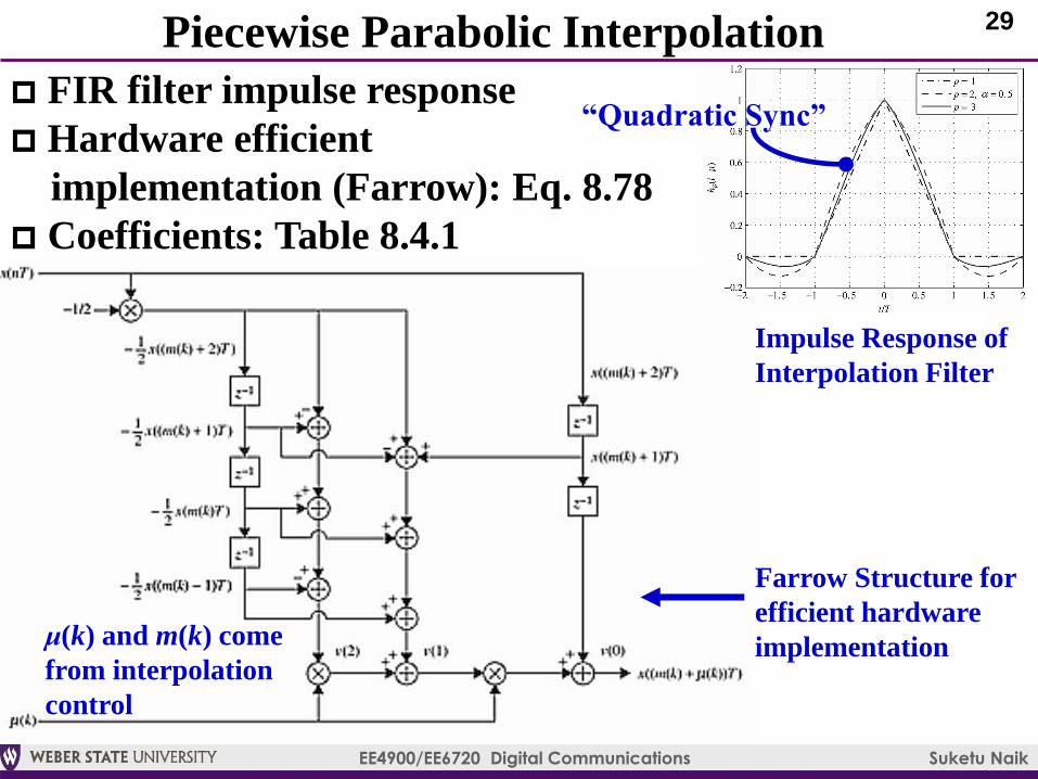
EE4900/EE6720 Digital Communications Suketu Naik
Piecewise Parabolic Interpolation
FIR filter impulse response
Hardware efficient
implementation (Farrow): Eq. 8.78
Coefficients: Table 8.4.1
“Quadratic Sync”
Impulse Response of
Interpolation Filter
Farrow Structure for
efficient hardware
implementationμ(k) and m(k) come
from interpolation
control

30
EE4900/EE6720 Digital Communications Suketu Naik
Discrete-time PLL for Symbol Timing
Four Components:
Interpolator & Timing Error Detector (TED)=>PD
Loop Filter F(z) => Loop Filter F(z)
Interpolation Control => DDS
From
Matched
Filter
To Decision
Block

31
EE4900/EE6720 Digital Communications Suketu Naik
Interpolation Control
Goal: provide the interpolator with a strobe signal that
indicates the kth basepoint index m(k) and kth interval μ(k)
Two methods:
Modulo-1 Counter Interpolation Control
Recursive Interpolation Control
Underflow
Strobe
Signal
m(k)
μ(k)

32
EE4900/EE6720 Digital Communications Suketu Naik
Modulo-1 Counter Interpolation Control
Decrementing counter: decrements by 1/N so that underflow
occurs every N samples
Loop filter output v(n) adjusts the decrement number
m can be viewed as “alignment clock”, mu = alighment
period
Underflow
Strobe
Signal
m(k)
μ(k)
Interpolation
Control ≈ DDS

33
EE4900/EE6720 Digital Communications Suketu Naik
Modulo-1 Counter Interpolation Control

34
EE4900/EE6720 Digital Communications Suketu Naik
Discrete-time PLL for Symbol Timing
Four Components:
Interpolator & Timing Error Detector (TED)=>PD
Loop Filter F(z) => Loop Filter F(z)
Interpolation Control => DDS
From
Matched
Filter
To Decision
Block

35
EE4900/EE6720 Digital Communications Suketu Naik
Proportional-Plus-Integrator Loop Filter
Loop Transfer Function Loop Constants
Eq. C.51Eq. C.61
From
TED
To
Interpolation
Control

36
EE4900/EE6720 Digital Communications Suketu Naik
Discrete-time
M-ary QAM

37
EE4900/EE6720 Digital Communications Suketu Naik
Discrete-time MQAM Symbol Timing
Goal: given I & Q components at a symbol rate and
corresponding sampling rate, find the optimum sampling
instant
Generic MQAM
Symbol Timing Sync

38
EE4900/EE6720 Digital Communications Suketu Naik
Discrete-time MQAM Symbol Timing
All components are the same as MPAM except two
interpolators (one for I and one for Q) and two TEDs (one for I
and one for Q)
M.F. outputs: x(nT)= Eq. 8.23 x cos, y(nT)=Eq. 8.23 x sin
ZCTED error signal: Eq. 8.100 with I estimates ෝ𝒂𝟎(k-1), ෝ𝒂𝟎(k)
and Q estimates ෝ𝒂𝟏(k-1), ෝ𝒂𝟏(k)