lecture 5 pn junctions - alexandria...
TRANSCRIPT

Lecture 5
pn Junctions
pn junctions 1-1

Outline I-V characteristics
Bias voltage Forward and reverse currents Reverse breakdown
Special purpose diodes Light Emitting Diode (LED)
Diode circuit analysis approaches Graphical analysis (load-line method) Simplified analysis with ideal diode model Simplified analysis using constant voltage drop Simplified analysis using piecewise-linear
equivalent circuit
pn junctions 1-2

Test Yourself
The status where no external forces such as voltages, electric fields, magnetic fields, or temperature gradients are acting on pn junctions is called:
i. reverse bias ii. thermal equilibrium (zero bias) iii. forward bias
The charge condition in which semiconductor crystals exist when operating at thermal equilibrium is called:
i. negatively charged ii. positively charge iii. charge-neutrality
pn junctions 1-3
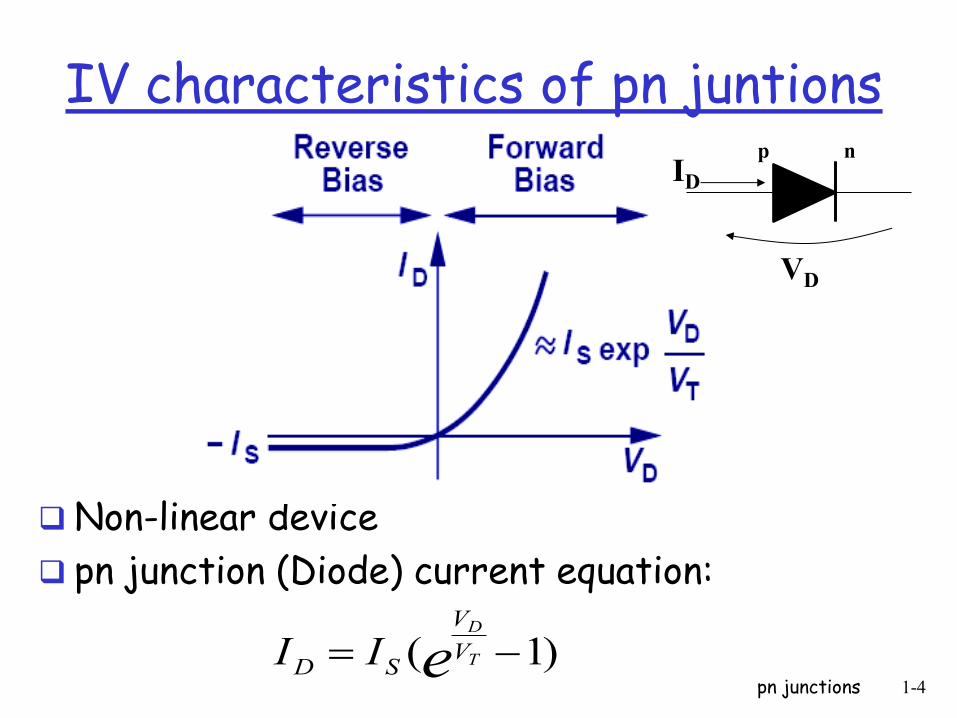
IV characteristics of pn juntions
Non-linear device
pn junction (Diode) current equation:
pn junctions 1-4
)1( e T
D
V
V
SD II
p n
VD
ID

Physics of forward bias:
pn junctions 1-5
• Potential drop across SCR reduced by VFB
• minority carrier injection in QNRs • Minority carrier diffusion through QNRs • Minority carrier recombination at contacts to the QNRs
(and surfaces) • Large supply of carriers injected into the QNRs
e T
D
V
V
DI
+ ve - ve
VFB

Physics of reverse bias
pn junctions 1-6
• Potential drop across SCR increased by VRB
• minority carrier extraction from QNRs • Minority carrier diffusion through QNRs • Minority carrier generation at surfaces & contacts of
QNRs • Very small supply of carriers available for extraction I saturates to small value (scale of nanoamperes)
+ ve - ve
VRB

pn junctions 1-7

pn junctions 1-8

pn junctions 1-9
Temperature Effects
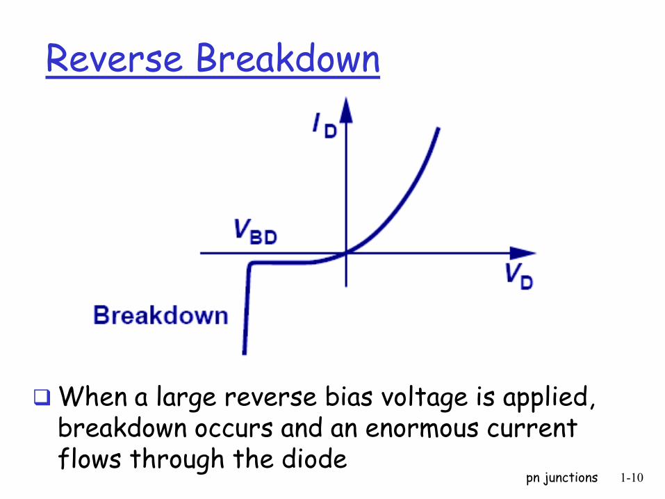
Reverse Breakdown
When a large reverse bias voltage is applied, breakdown occurs and an enormous current flows through the diode
pn junctions 1-10

Diode Capacitance
pn junctions 1-11
• Biasing a diode forms a volume of charges stored inside this diode and accordingly leading to have diode capacitance (no charge-neutrality)
• Changing diode biasing from reverse to forward or vice versa leads to change in the volume of charges stored in the diode and also the width of the depletion layer or SCR
• This results in a change in the diode capacitance
Depletion or Junction
Capacitance
Diffusion
Capacitance

Special purpose diodes
Light Emitting Diode (LED) In a forward-biased p-n junction,
recombination of the holes and electrons requires energy possessed by the unbounded free electrons
In Si and Ge, most of the energy is dissipated in the form of heat and photons (cause: indirect band gap)
But in other materials such as GaAs, the outcome of hole-electron recombination processes is light but it is invisible for the eye to see (infrared)
Other materials emit visible light during forward-bias operation
pn junctions 1-12
Color Construction Forward Voltage
Green
Orange
Red
GaP
GaAsP
GaAsP
2.2
2.0
1.8

Diode Circuit Analysis
Why ? Analyze operation of diodes
One common objective of diode circuit analysis is to find the quiescent operating point (Q-point), or bias point, for the diode
Enable knowing range of diode voltage and current due to input alternating signals
The Q-point consists of the dc current and bias voltage (ID, VD) that defines the point of operation on the diode’s IV characteristic curve
pn junctions 1-13

Practical Aspects of pn Junction
The left hand diagram shows reverse bias, with positive on the cathode and negative on the anode (via the lamp). No current flows
The other diagram shows forward bias, with positive on the anode and negative on the cathode. A current flows
pn junctions 1-14
anode
cathode
Forward bias
Reversed bias Lamp off
Lamp on

Polarization of the pn Junction
Examples of forward biasing circuits
pn junctions 1-15

Polarization of the pn Junction
Examples of reverse biasing circuits
pn junctions 1-16
Graphical analysis (load-line method) Series diode circuit and
Characteristic curve
Connect a line between E / R
and E The overlap of the lines
becomes the Q-point of the
diode and IDQ and VDQ
will be obtained
pn junctions 1-17
IRVVVE DRD
REI ,RIRI0E ,0VFor DDDD
EV ,VR)0(VE ,0IFor DDDD

Example Determine ID, VD & VR
pn junctions 1-18
RIVVVE DDRD
mA 24.2433.0
8
0 ,0
kREI
RIEV
D
DD
V 8
)0( ,0
EV
RVEI
D
DDR
E
E
Q-point
DQI
DQV
From the analysis: VDQ = VD ≈ 0.9 V IDQ = ID ≈ 21.5 mA For VR,
V 095.7)k33.0)(m5.21(RIV DR

Diode Approximation
Diode modeling circuits: Ideal equivalent circuit (ideal diode analysis)
Simplified equivalent circuit (constant voltage drop (CVD))
Piecewise-linear equivalent circuit
pn junctions 1-19

Ideal Diode Characteristics
Ideal diode in Reverse Biased acts as an open-circuited (O/C) device and in Forward Biased acts as a short-circuited (S/C) device
pn junctions 1-20
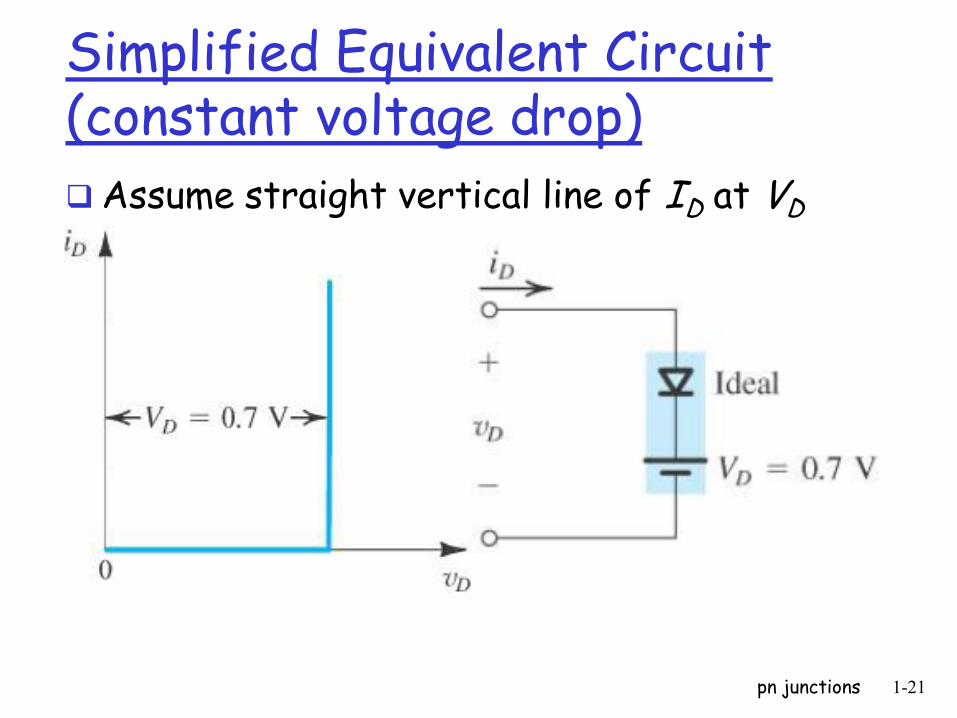
Simplified Equivalent Circuit (constant voltage drop)
Assume straight vertical line of ID at VD
pn junctions 1-21
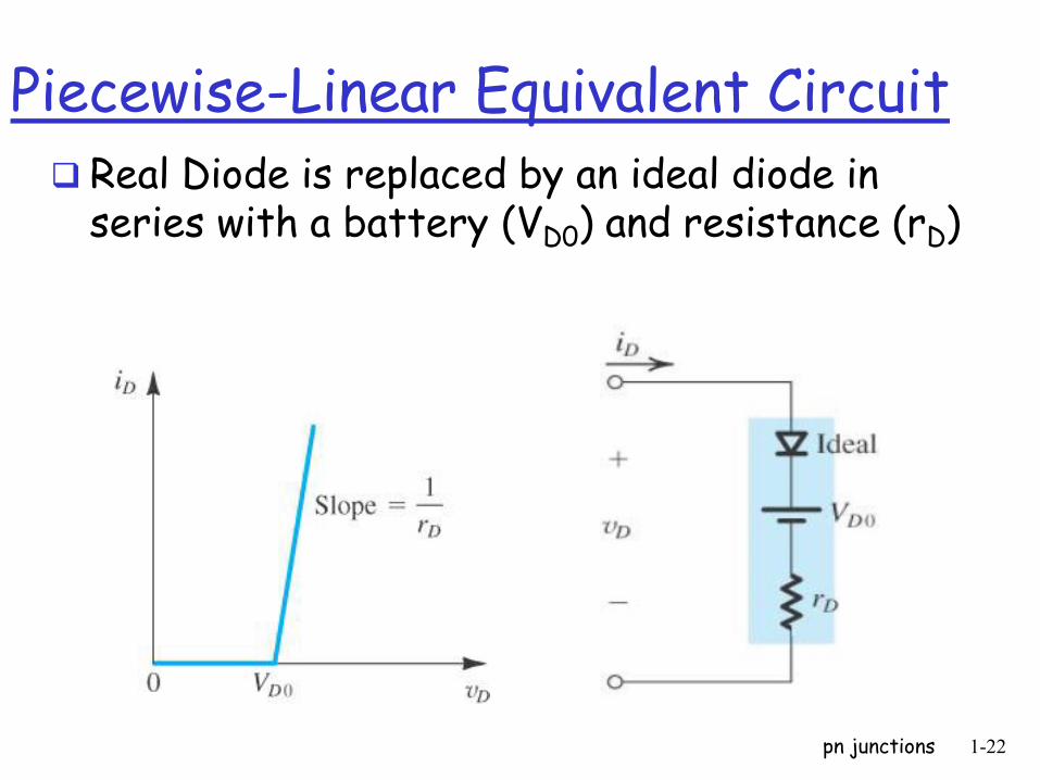
Piecewise-Linear Equivalent Circuit Real Diode is replaced by an ideal diode in
series with a battery (VD0) and resistance (rD)
pn junctions 1-22

pn junctions 1-23
Lecture Summary Covered material Continue pn junctions
I-V characteristics Diode circuit analysis approaches
• Graphical analysis (load-line method) • Simplified analysis with ideal diode model • Simplified analysis using constant voltage drop • Simplified analysis using piecewise-linear equivalent circuit
Material to be covered next lecture
Examples on DC analysis of pn junctions Analysis of AC equivalent diode circuits