lecture 6 sequential circuits and memory 6 sequential circuits and memory . outline 2 . sr latch •...
TRANSCRIPT

Xuan ‘Silvia’ Zhang Washington University in St. Louis
http://classes.engineering.wustl.edu/ese566/
Lecture 6 Sequential Circuits and Memory
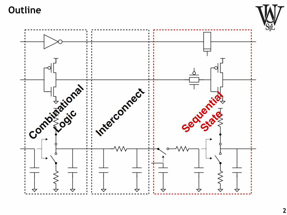
Outline
2

SR Latch
• Basic NOR latch
3
S (set)
R (reset) Q
Q
S
R
0
0
not allowed
Q
Q
1
0
tpd
set
reset
unstable No change
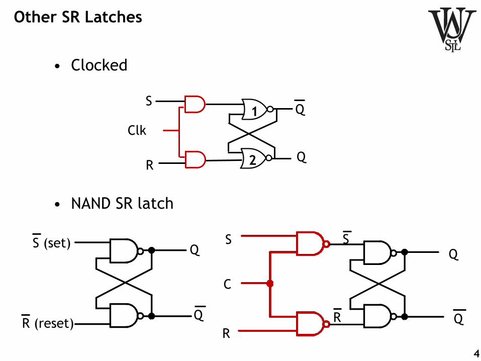
Other SR Latches
• Clocked
• NAND SR latch
4
1
2
Q
Q
S
R
Clk
Q S (set)
R (reset) Q
S
R
C
Q
Q
S
R

D Latch
• Truth table
5
S R Q+ Q+ 0 0 hold, 0 1 0 1 1 0 1 0 1 1 0 0
SR latch:
C
D Q
Q
D Q
C
Q
D Q(t+1) 0 0 1 1
D latch

Level-Sensitive Latch
6

Flip-Flop
• Latch timing issue – transparent when C = 1 – state should change only once every new clock cycle
• Master-slave flip flop – break feedthrough
7
Combina-tional Logic D Latch
(storage)
Inputs Outputs
State Next State
X0 X1 X0 X1
X2
C=0
X1 X1 X1 X2 X3
→1
C
S
R
Q
Q
Q
Q
C R
Q
Q
C
S
R
S Y
/Y

Flip-Flop Timing Issue
• 1’ catching
8
C
S
R
Y
Q Slave out
Master out
Master active
Slave active
1’ catching
wrong output should have been 0
C
S
R
Q
Q
Q
Q
C R
Q
Q
C
S
R
S Y
Y’
Glitch

Edge-Triggered D Flip-Flop (DFF)
• Why edge trigger? • D replace S and R input
9
C
S
R
Q
Q C
Q
Q C
D Q D
Q
C
D
Y
Q Slave out
Master out
Master active
Slave active no 1’ catching
correct output
Y

Edge-Sensitive Flip-Flop
10

Outline
Sequential Circuits Timing Analysis Memory
11
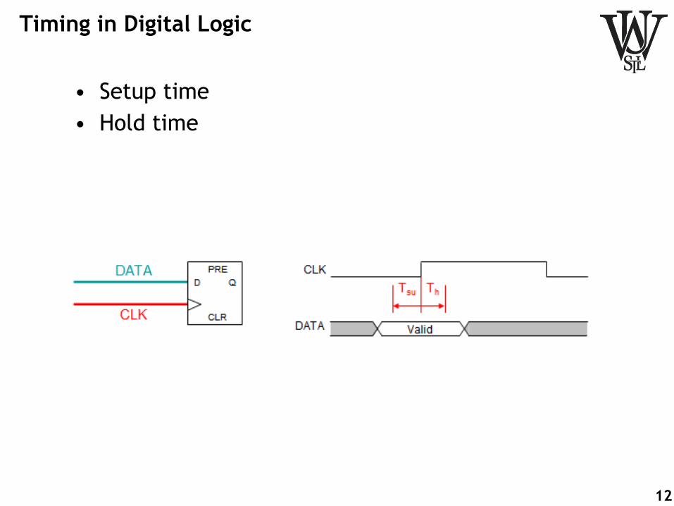
Timing in Digital Logic
• Setup time • Hold time
12

Timing in Digital Logic
• Launch edge and latch edge
13

Timing in Digital Logic
• Data arrival time: using launch edge
Tclk Clock Skew
Tco FF Clock-> Output
Tdata Logic Delay
14

Timing in Digital Logic
• Clock arrival time
15

Timing in Digital Logic
• Data required time (setup): latch edge
16

Timing in Digital Logic
• Data required time (hold): next launch = latch
17

Timing in Digital Logic
• Setup slack
18

Timing in Digital Logic
• Hold slack
19
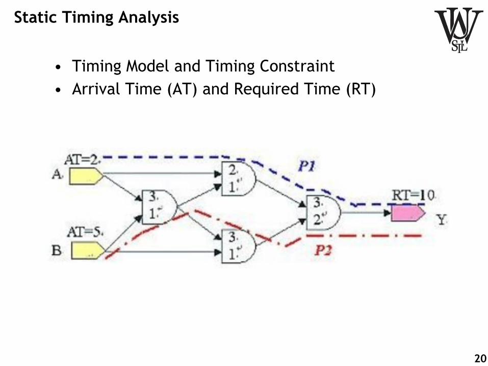
Static Timing Analysis
• Timing Model and Timing Constraint • Arrival Time (AT) and Required Time (RT)
20

Outline
Sequential Circuits Timing Analysis Memory
21

Static RAM
• Applications – CPU register file, cache, embedded memory, DSP
• Characteristics – 6 transistor per cell, other topologies – no need to refresh – access time ~ cycle time – no charge to leak – faster, more area, more expensive
22

SRAM Operation
• Standby – word line de-asserted
• Read – precharge bit lines – assert WL – BL rise/drop slightly
• Write – apply value to BL – assert WL – input drivers stronger
23

SRAM Architecture
24
source: semiengineering.com

Multi-Bank Layout
25
source: semiengineering.com

Questions?
Comments?
Discussion?
26

Design Tool Tutorials
• Standard-cell based design flow
27

Design Tool Tutorials
• Functional Simulation – tool: Synopsys VCS – simulate your HDL (eg. Verilog) code to verify
functionality
• Logic Synthesis – tool: Synopsys Design Compiler (DC) – convert/synthesize behavioral/RTL level HDL to gate-
level netlist (i.e. connectivity list)
• Physical Design (Place & Route) – tool: Cadence Encounter – given the gate-level netlist, place and route the design
to complete an IC chip in its final physical form
28

Acknowledgement
Jan Rabaey, “Digital Integrated Circuits”, 2006 Cornell University, ECE 5745
29