lecture 9 - pdfs.semanticscholar.org
TRANSCRIPT

Power Electronics Lab 1
Lecture 9ECEN 4517/5517
Experiment 4
Lecture 8: Step-up dc-dc converter
Lecture 9: Design of analog feedback loop
Part I—Controller IC:Demonstrate operating
PWM controller IC (UC 3525)
Part II—Power Stage:Demonstrate operating
power converter (cascaded boost converters)
Part III—Closed-Loop Analog Control System:Demonstrate analog feedback system that regulates the dc output voltage
Measure and document loop gain and compensator design
Power Electronics Lab 2
Due dates
This week in lecture (Mar. 13):Prelab assignment for Exp. 4 (one from every student)
This week in lab (Mar. 13-15):Start Exp. 4
Next week in lab(Mar. 20):Exp. 3 part 2 report due at beginning of lab
After Spring break, in lecture (Apr. 3):Quiz on Exp. 3 Part 1

Power Electronics Lab 3
Exp. 4 Part IIIRegulation of output voltage via feedback
• Model and measure control-to-output transfer function Gvd(s)
• Design and build feedback loop
• Demonstrate closed-loop regulation of vHVDC

ECEN 4517 11
Negative feedback:a switching regulator system
+–
+
v
–
vg
Switching converterPowerinput
Load–+
Compensator
vref
Referenceinput
HvPulse-widthmodulator
vc
Transistorgate driver
Gc(s)
H(s)
ve
Errorsignal
Sensorgain
iload
ECEN 4517 12
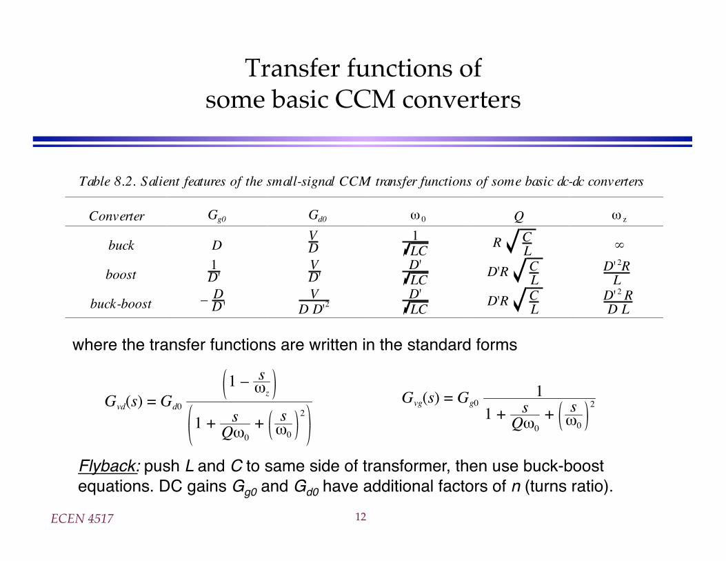
Transfer functions ofsome basic CCM converters
Table 8.2. Salient features of the small-signal CCM transfer functions of some basic dc-dc converters
Converter Gg0 Gd0 0 Q z
buck D VD
1LC
R CL
boost 1D'
VD'
D'LC
D'R CL
D' 2RL
buck-boost – DD '
VD D'2
D'LC
D'R CL
D' 2 RD L
where the transfer functions are written in the standard forms
Gvd(s) = Gd0
1 – sz
1 + sQ 0
+ s0
2
Gvg(s) = Gg01
1 + sQ 0
+ s0
2
Flyback: push L and C to same side of transformer, then use buck-boost equations. DC gains Gg0 and Gd0 have additional factors of n (turns ratio).

ECEN 4517 13
Bode plot: control-to-output transfer functionbuck-boost or flyback converter example
f
0˚
–90˚
–180˚
–270˚
Gvd
Gd0 = 187 V 45.5 dBV
Gvd Gvd
0 dBV
–20 dBV
–40 dBV
20 dBV
40 dBV
60 dBV
80 dBV
Q = 4 12 dB
fz2.6 kHz
RHP Gvd
10-1/2Q f0
101/2Q f0
0˚ 300 Hz
533 Hz
–20 dB/decade
–40 dB/decade
–270˚
fz /10260 Hz
10fz26 kHz
1 MHz10 Hz 100 Hz 1 kHz 10 kHz 100 kHz
f0400 Hz
ECEN 4517 14
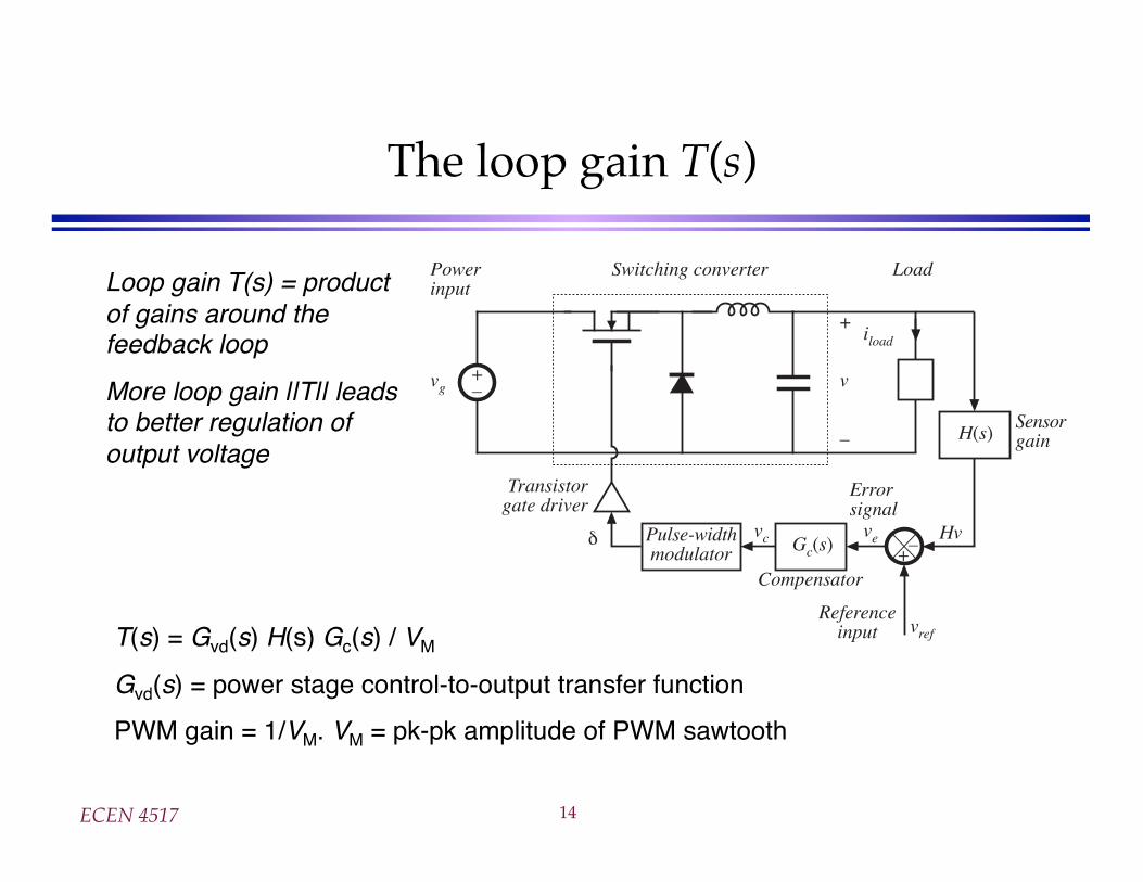
The loop gain T(s)
+–
+
v
–
vg
Switching converterPowerinput
Load
–+
Compensator
vref
Referenceinput
HvPulse-widthmodulator
vc
Transistorgate driver
Gc(s)
H(s)
ve
Errorsignal
Sensorgain
iload
Loop gain T(s) = product of gains around the feedback loop
More loop gain ||T|| leads to better regulation of output voltage
T(s) = Gvd(s) H(s) Gc(s) / VM
Gvd(s) = power stage control-to-output transfer function
PWM gain = 1/VM. VM = pk-pk amplitude of PWM sawtooth
ECEN 4517 15
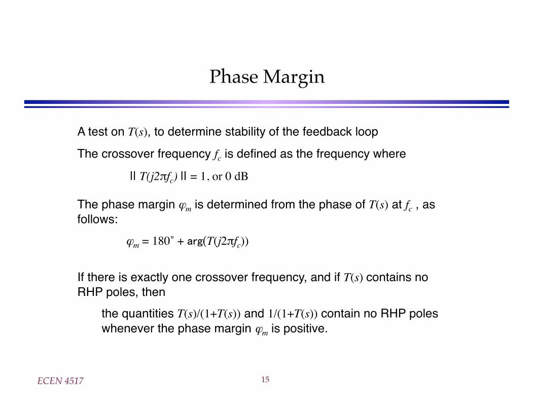
Phase Margin
A test on T(s), to determine stability of the feedback loop
The crossover frequency fc is defined as the frequency where
|| T(j2 fc) || = 1, or 0 dB
The phase margin m is determined from the phase of T(s) at fc , as follows:
m = 180˚ + (T(j2 fc))
If there is exactly one crossover frequency, and if T(s) contains no RHP poles, then
the quantities T(s)/(1+T(s)) and 1/(1+T(s)) contain no RHP poles whenever the phase margin m is positive.
ECEN 4517 16
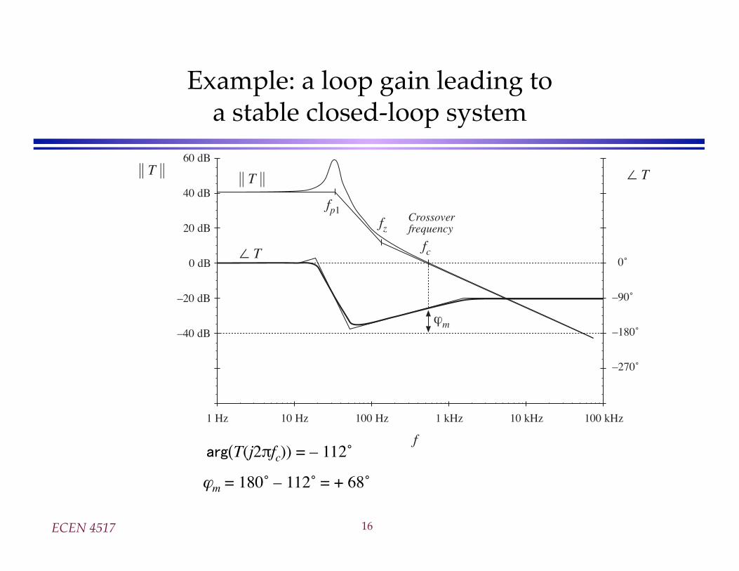
Example: a loop gain leading toa stable closed-loop system
(T(j2 fc)) = – 112˚
m = 180˚ – 112˚ = + 68˚
fc
Crossoverfrequency
0 dB
–20 dB
–40 dB
20 dB
40 dB
60 dB
f
fp1fz
T
0˚
–90˚
–180˚
–270˚
m
T
T T
1 Hz 10 Hz 100 Hz 1 kHz 10 kHz 100 kHz

ECEN 4517 17
Transient response vs. damping factor
0
0.5
1
1.5
2
0 5 10 15
ct, radians
Q = 10
Q = 50
Q = 4
Q = 2
Q = 1
Q = 0.75
Q = 0.5
Q = 0.3
Q = 0.2
Q = 0.1
Q = 0.05
Q = 0.01
v(t)
ECEN 4517 18
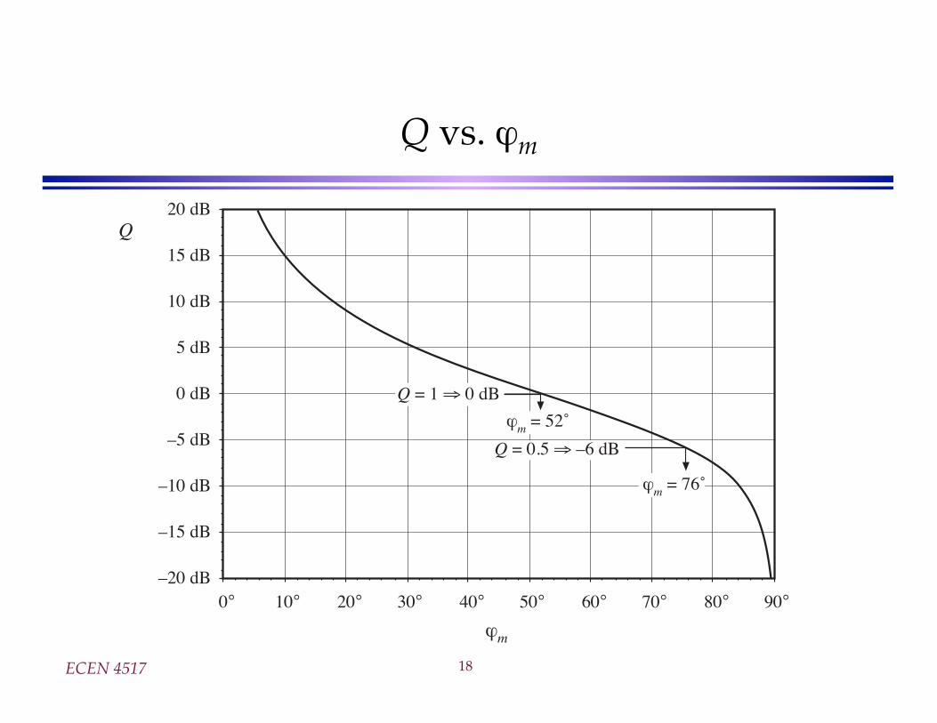
Q vs. m
0 10 20 30 40 50 60 70 80 90
m
Q
Q = 1 0 dB
Q = 0.5 –6 dBm = 52˚
m = 76˚
–20 dB
–15 dB
–10 dB
–5 dB
0 dB
5 dB
10 dB
15 dB
20 dB
Fundamentals of Power Electronics Chapter 9: Controller design42
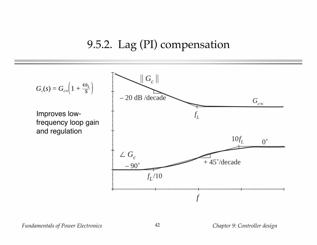
9.5.2. Lag (PI) compensation
Gc(s) = Gc∞ 1 +ωLs
Improves low-frequency loop gainand regulation
f
|| Gc ||
∠ Gc
Gc∞
0˚
fL/10
+ 45˚/decade
fL
– 90˚
10fL
– 20 dB /decade
Fundamentals of Power Electronics Chapter 9: Controller design43
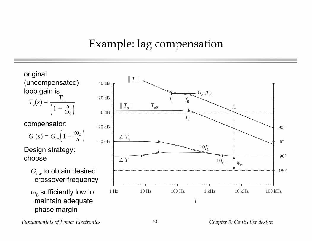
Example: lag compensation
original(uncompensated)loop gain is
Tu(s) =Tu0
1 + sω0
compensator:Gc(s) = Gc∞ 1 +
ωLs
Design strategy:choose
Gc∞ to obtain desiredcrossover frequencyωL sufficiently low tomaintain adequatephase margin
0 dB
–20 dB
–40 dB
20 dB
40 dB
f
90˚
0˚
–90˚
–180˚
Gc∞Tu0fL
f0
Tu0
∠ Tu
|| Tu ||f0
|| T ||
fc
∠ T
10fL
10f0 ϕm
1 Hz 10 Hz 100 Hz 1 kHz 10 kHz 100 kHz

Fundamentals of Power Electronics Chapter 8: Converter Transfer Functions94
8.4. Measurement of ac transfer functionsand impedances
Network Analyzer
Injection source Measured inputs
vy
magnitudevz
frequencyvz
outputvz
+ –
input
vx
input+ – + –
vy
vx
vy
vx
Data
17.3 dB
– 134.7˚
Data busto computer

Fundamentals of Power Electronics Chapter 8: Converter Transfer Functions95
Swept sinusoidal measurements
• Injection source produces sinusoid of controllable amplitude andfrequency
• Signal inputs and perform function of narrowband trackingvoltmeter:
Component of input at injection source frequency is measuredNarrowband function is essential: switching harmonics and othernoise components are removed
• Network analyzer measures
vz
vx vy
∠vy
vx
vy
vx
and
Fundamentals of Power Electronics Chapter 8: Converter Transfer Functions96
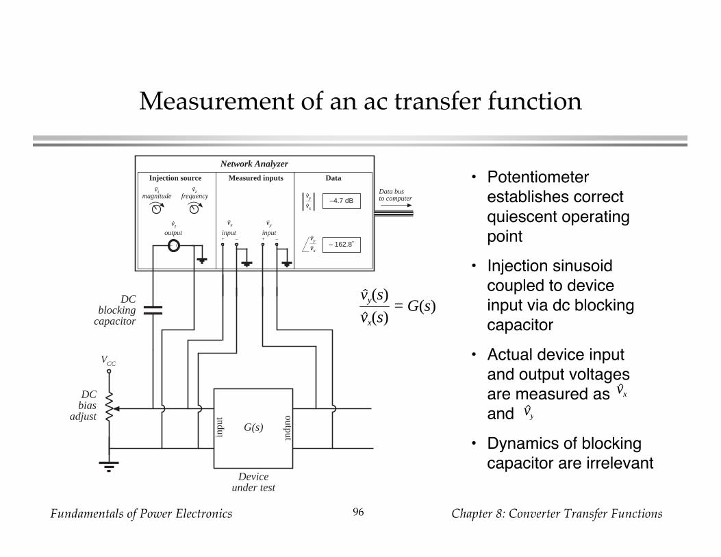
Measurement of an ac transfer function
Network Analyzer
Injection source Measured inputs
vy
magnitudevz
frequencyvz
outputvz
+ –
input
vx
input+ – + –
vy
vx
vy
vx
Data
–4.7 dB
– 162.8˚
Data busto computer
Deviceunder test
G(s)
inpu
t output
VCC
DCbias
adjust
DCblocking
capacitor
• Potentiometerestablishes correctquiescent operatingpoint
• Injection sinusoidcoupled to deviceinput via dc blockingcapacitor
• Actual device inputand output voltagesare measured asand
• Dynamics of blockingcapacitor are irrelevant
vx
vy
vy(s)
vx(s)= G(s)

Fundamentals of Power Electronics Chapter 9: Controller design64
9.6.1. Voltage injection
• Ac injection source vz is connected between blocks 1 and 2• Dc bias is determined by biasing circuits of the system itself• Injection source does modify loading of block 2 on block 1
+–
H(s)
+–
Z2(s)
Block 1 Block 2
0
Tv(s)
Z1(s) Zs(s)
– +
+
vx(s)
–
vref (s)G1(s)ve(s)
ve(s) G2(s)vx(s) = v(s)
–
vy(s)
+
vzi(s)
Power Electronics Lab 5
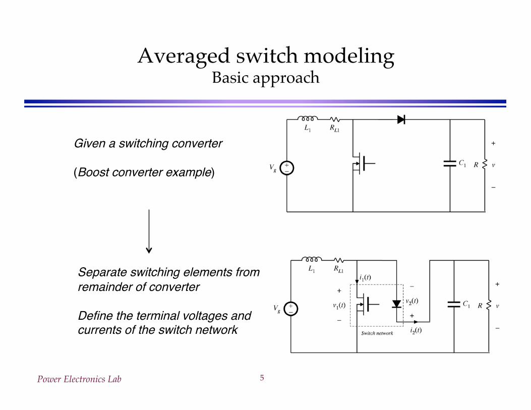
Averaged switch modelingBasic approach
Separate switching elements from remainder of converter
Define the terminal voltages and currents of the switch network
Given a switching converter
(Boost converter example)
ECEN 4517 14
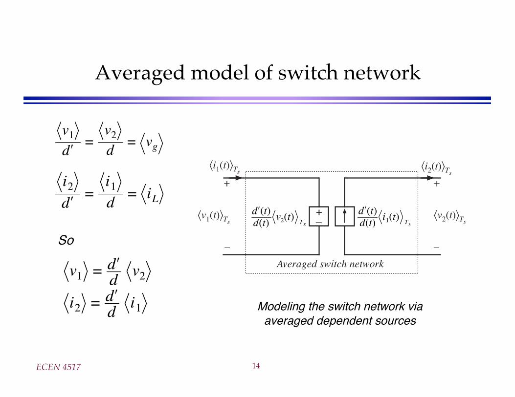
Averaged model of switch network
v1d
=v2d= vg
i2d
=i1d= iL
So
v1 =dd
v2
i2 =dd
i1
+–
+
v2(t) Ts
–
i1(t) Ts
Averaged switch network
+
v1(t) Ts
–
i2(t) Ts
d (t)d(t)
v2(t) Ts
d (t)d(t)
i1(t) Ts
Modeling the switch network viaaveraged dependent sources
ECEN 4517 22
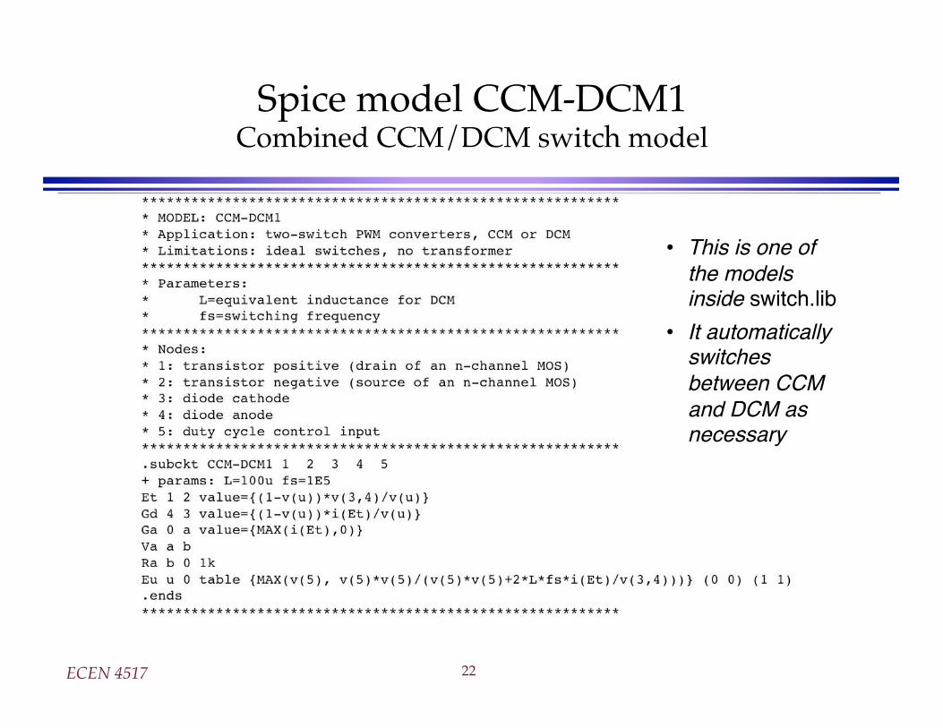
Spice model CCM-DCM1Combined CCM/DCM switch model
• This is one of the models inside switch.lib
• It automatically switches between CCM and DCM as necessary
Power Electronics Lab 4
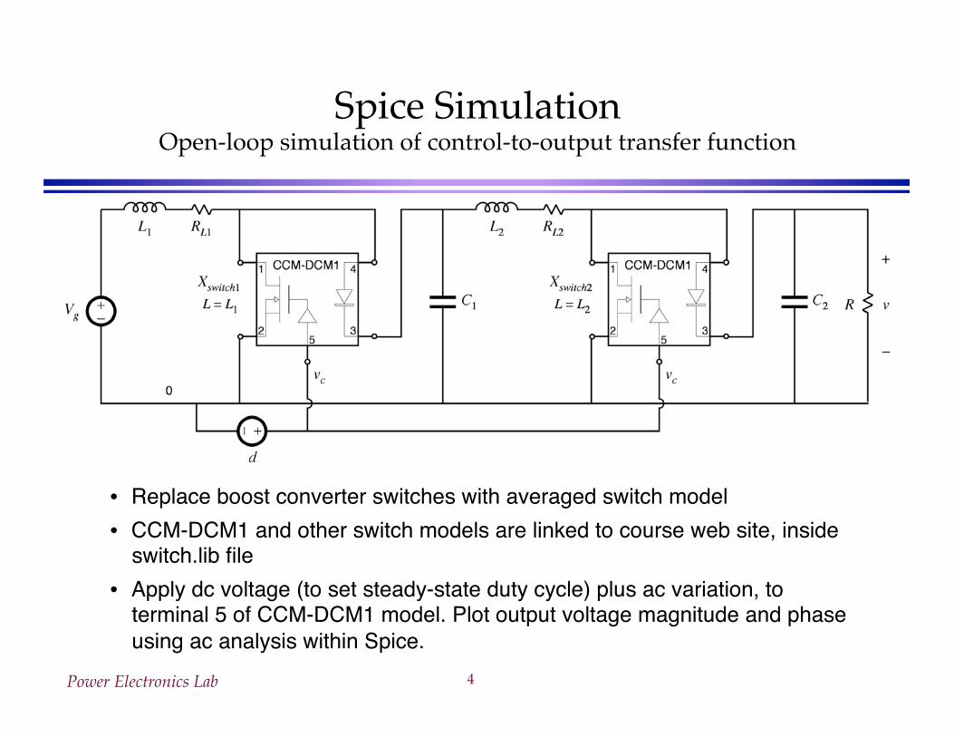
Spice SimulationOpen-loop simulation of control-to-output transfer function
• Replace boost converter switches with averaged switch model
• CCM-DCM1 and other switch models are linked to course web site, inside switch.lib file
• Apply dc voltage (to set steady-state duty cycle) plus ac variation, to terminal 5 of CCM-DCM1 model. Plot output voltage magnitude and phase using ac analysis within Spice.

ECEN 4517 16
Basic CCM SEPIC ExampleFrequency Response
Ideal SEPIC frequency response.lib switch.libVg 1 0 dc 120VL1 1 2x 800uHRL1 2x 2 1UC1 2 3 100uFL2 3 0 100uHC2 4 0 100uFRL 4 0 40Vc 5 0 dc 0.4 ac 1Rc 5 0 1MXswitch 2 0 4 3 5 CCM1.ac DEC 201 10 100kHz.PROBE.end
+–
1
2
3
45
CCM1
Vg
L1 RL1
C1
L2 C2 RL
1 22x 3 4
5
0
+– Rc

ECEN 4517 17
PROBE OutputSEPIC Example: Control-to-output transfer function
Magnitude
Phase
Power Electronics Lab 6
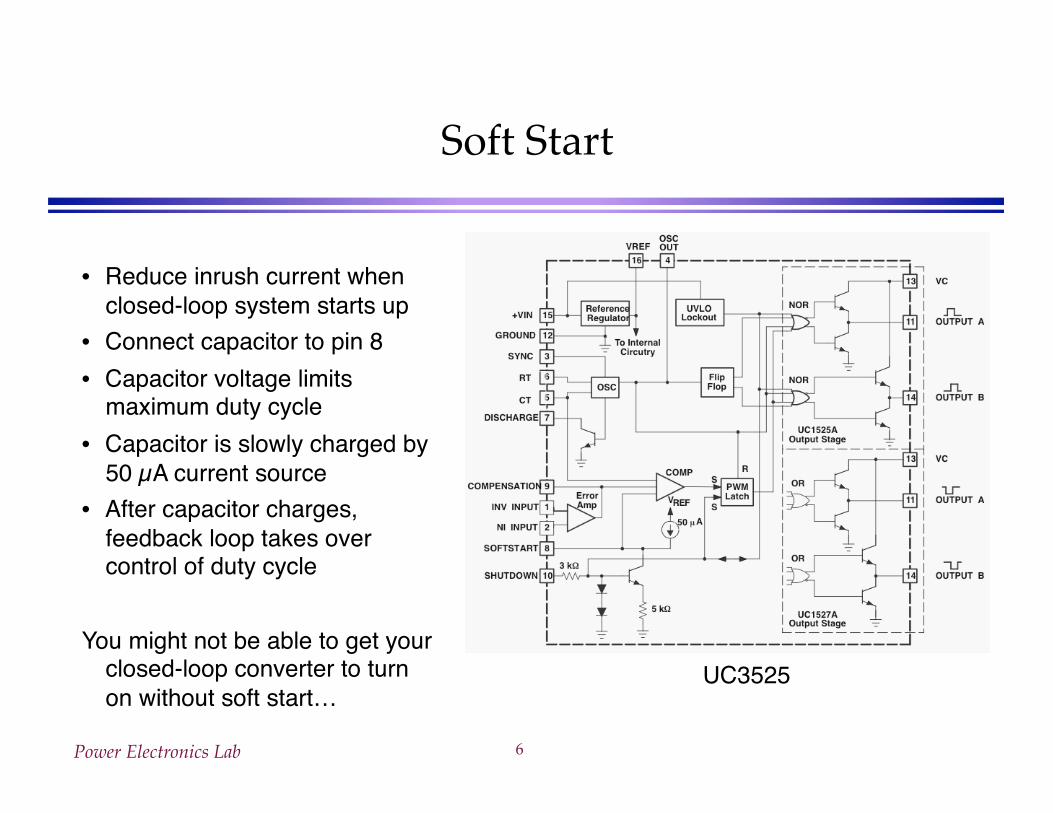
Soft Start
UC3525
• Reduce inrush current when closed-loop system starts up
• Connect capacitor to pin 8
• Capacitor voltage limits maximum duty cycle
• Capacitor is slowly charged by 50 μA current source
• After capacitor charges, feedback loop takes over control of duty cycle
You might not be able to get your closed-loop converter to turn on without soft start…