led lighting power controller - ti.com · corrected led driver •outdoor lighting: street,...
TRANSCRIPT

1FEATURES APPLICATIONS
DESCRIPTION
SIMPLIFIED APPLICATION DIAGRAM
1
2
3
4
8
7
6
5
VDD
GDRV
GND
TZE
VSENSE
EAOUT
VINS
ISENSE
UCC28810
+
Triac Dimming
Detect
Low Pass
Filter
+
Bias
LED
Current
Sense
UDG-08120
Bias
UCC28810UCC28811
www.ti.com .............................................................................................................................................................................................. SLUS865–OCTOBER 2008
LED LIGHTING POWER CONTROLLER
• AC Input General Lighting Applications Using• Transition Mode Controller for LowHB LEDsImplementation Cost of AC Input LED Lighting
• Industrial, Commercial and ResidentialApplicationsLighting Fixtures• Implements Single Stage Power Factor
• Outdoor Lighting: Street, Roadway, Parking,Corrected LED DriverConstruction and Ornamental LED Lighting• Enhanced Transient Response With Slew-Rate Fixtures
Comparator• Interfaces with Traditional Wall Dimmers• Accurate Internal VREF for Tight Output The UCC28810 and UCC28811 are general lightingRegulation power controllers for low to medium power lumens• Two UVLO Options applications requiring power factor correction and
EMC compliance. It is designed for controlling a• Overvoltage Protection (OVP), Open-Feedbackflyback, buck or boost converter operating in criticalProtection and Enable Circuitsconduction mode. It features a transconductance
• ±750-mA Peak Gate Drive Current voltage amplifier for feedback error processing, a• Low Start-Up and Operating Currents simple current reference generator for generating a
current command proportional to the input voltage, a• Lead (Pb)-Free Packagescurrent-sense (PWM) comparator, PWM logic and atotem-pole driver for driving an external FET.
1
Please be aware that an important notice concerning availability, standard warranty, and use in critical applications of TexasInstruments semiconductor products and disclaimers thereto appears at the end of this data sheet.
PRODUCTION DATA information is current as of publication date. Copyright © 2008, Texas Instruments IncorporatedProducts conform to specifications per the terms of the TexasInstruments standard warranty. Production processing does notnecessarily include testing of all parameters.

DESCRIPTION (CONTINUED)
ABSOLUTE MAXIMUM RATINGS (1)
UCC28810UCC28811SLUS865–OCTOBER 2008.............................................................................................................................................................................................. www.ti.com
In the critical conduction mode operation, the PWM circuit is self-oscillating with the turn-on being governed by atransformer zero energy detector (TZE pin) and the turn-off being governed by the current sense comparator.Additionally, the controller provides features such as peak current limit, restart timer, overvoltage protection(OVP), and enable.
The efficient system performance is attained by incorporation of zero power detect function which allows thecontroller output to shut down at light load conditions without running into overvoltage. The device also featuresan innovative slew rate enhancement circuit which improves the large signal transient performance of the voltageerror amplifier. The low start-up and operating currents of the device result in low power consumption and easeof start-up. The highly-accurate internal bandgap reference leads to tight regulation of the output voltage innormal and OVP conditions, resulting in higher system reliability. The enable comparator ensures that thecontroller is off if the feedback sense path is broken or if the input voltage is very low.
There are two key parametric differences between UCC28810 and UCC28811, the UVLO turn-on threshold andthe gM amplifier source current. The UVLO turn-on threshold of the UCC28810 is 15.8 V and for the UCC28811 itis 12.5 V. The gM amplifier source current for UCC28810 is typically 1.3 mA, and for the UCC28811 it is 300µA.The higher UVLO turn-on threshold of the UCC28810 allows quicker and easier start-up with a smaller VDDcapacitance while the lower UVLO turn-on threshold of UCC28811 allows operation of the critical conductionmode controller to be easily controlled by the downstream PWM controller in two-stage power converters. TheUCC28810 gM amplifier also provides a full 1.3-mA typical source current for faster start-up and improvedtransient response when the output is low either at start-up or during transient conditions. The UCC28811 issuitable for applications such as street lights and larger area luminaires where a two-stage power conversion isneeded. The UCC28810 is suitable for applications such as commercial or residential retrofit luminaires wherethere is no down-stream PWM conversion and the advantages of smaller VDD capacitor and improved transientresponse can be realized.
Devices are available in the industrial temperature range of –40°C to 105°C. Package offering is an 8-pin SOIC(D) package.
ORDERING INFORMATION (1)
UVLO THRESHOLD gM AMPLIFIERPIN ORDERABLEVOLTAGE (V)TA = TJ SOURCE CURRENT PACKAGE SUPPLYCOUNT DEVICE NUMBER
(µA)ON OFFTube of 80 UCC28810D
15.8 9.7 –1300Reel of 2500 UCC28810DR
–40°C to 105°C D 8Tube of 80 UCC28811D
12.5 9.7 –300Reel of 2500 UCC28811DR
(1) D (SOIC-8) package is available taped and reeled. Add R suffix to device type (e.g. UCC28810DR) to order quantities of 2,500 devicesper reel.
VALUE UNIT
VDD (Internally clamped) 20Input voltage
VSENSE, VINS, ISENSE 5 VMinimum input VSENSE, VINS, ISENSE –5voltage
VDD 30Input current mA
TZE ±10
Output current GDRV ±750 mA
Output voltage GDRV –5 V
Tstg Storage temperature –55 to 150
TJ Operating temperature –65 to 150 °C
Soldering temperature 300
(1) Permanent device damage may occur if Absolute Maximum Ratings are exceeded. Exposure to conditions beyond the operationallimits for extended periods of time may affect device reliability. Currents are positive into, and negative out of the specified terminal.
2 Submit Documentation Feedback Copyright © 2008, Texas Instruments Incorporated
Product Folder Link(s): UCC28810 UCC28811

PACKAGE DISSIPATION RATINGS (1)
UCC28810UCC28811
www.ti.com .............................................................................................................................................................................................. SLUS865–OCTOBER 2008
PACKAGE THERMAL IMPEDANCE JUNCTION-TO-AMBIENT (°C/W)
Plastic 8-Pin Small Outline 150
(1) TI device packages are modeled and tested for thermal performance using printed circuit boarddesigns outlined in JEDEC standards JESD 51-3 and JESD 51-7.
Copyright © 2008, Texas Instruments Incorporated Submit Documentation Feedback 3
Product Folder Link(s): UCC28810 UCC28811

ELECTRICAL CHARACTERISTICS
UCC28810UCC28811SLUS865–OCTOBER 2008.............................................................................................................................................................................................. www.ti.com
–40°C ≤ TA = TJ ≤ 105°C, VVDD = 12 VDC, CGDRV = 0.1-µF from VDD to GND, all voltages are with respect to GND.
PARAMETER TEST CONDITIONS MIN TYP MAX UNITSUPPLYVVDD Operating voltage 18
VShunt voltage IVDD = 25 mA 18 19 20Supply current, off VVDD = VVDD turn-on threshold –300 mV 75 125 µASupply current, disabled VVSENSE = 0.5 V 2 4
IVDD Supply current, on 75 kHz, CGDRV = 0 nF 4 6 mASupply current, dynamic operating 75 kHz, CGDRV = 1 nF 5 7
UVLOUCC28810 15.4 15.8 16.4
VDD turn-on thresholdUCC28811 12.0 12.5 13.0 V
VDD turn-off threshold 9.4 9.7 10.0UCC28810 5.8 6.3 6.8
VUVLO UVLO hysteresis VUCC28811 2.3 2.8 3.3
VOLTAGE AMPLIFIER (VSENSE)VREF Internal voltage reference 2.45 2.50 2.55 VIBIAS Input bias current 0.5 µA
EAOUT high VVSENSE = 2.1 V 4.5 5.5 VEAOUT low VVSENSE = 2.55 V 1.80 2.45 V
gM Transconductance TJ = 25°C, VEAOUT = 3.5 V 60 90 130 µSUCC28810 –0.2 –1.0 mA
IEAOUT,SRC Source current VVSENSE = 2.1 V, VEAOUT = 3.5 VUCC28811 –200 –300 –400 µA
IEAOUT,SNK Sink current VVSENSE = 2.1 V, VEAOUT = 3.5 V 0.2 1.0 mAOVERVOLTAGE PROTECTION / ENABLE (VSENSE)
VVREF+ VVREF VVREFUCC28810 0.165 +0.190 +0.210VOV(ref) Overvoltage reference V
VVREF+ VVREF+ VVREF+UCC28811 0.150 0.180 0.210UCC28810 175 200 225
Hysteresis mVUCC28811 150 180 210UCC28810 0.62 0.67 0.72
Enable threshold VUCC28811 0.18 0.23 0.28
Enable hysteresis 0.05 0.10 0.20 VCURRENT REFERENCE GENERATORK Current reference generator gain constant VVINS = 0.5 V, VEAOUT = 3.5 V 0.43 0.65 0.87 1/V
Dynamic input range, VVINS INPUT 0 to 2.5 0 to 3.5 V2.5 to 2.5 toVEAOUT Error amplifier dynamic input range V3.8 4.0
Input bias current, VINS 0.1 1.0 µA
4 Submit Documentation Feedback Copyright © 2008, Texas Instruments Incorporated
Product Folder Link(s): UCC28810 UCC28811

UCC28810UCC28811
www.ti.com .............................................................................................................................................................................................. SLUS865–OCTOBER 2008
ELECTRICAL CHARACTERISTICS (continued)–40°C ≤ TA = TJ ≤ 105°C, VVDD = 12 VDC, CGDRV = 0.1-µF from VDD to GND, all voltages are with respect to GND.
PARAMETER TEST CONDITIONS MIN TYP MAX UNITZERO POWERVEAOUT Zero power comparator threshold (1) 2.1 2.3 2.5 VTRANSFORMER ZERO ENERGY DETECT
Input threshold (rising edge) (1) 1.00 1.25 1.80 VHysteresis (1) 250 350 450 mVInput high clamp ITZE = 3 mA 5 6 VInput low clamp ITZE = –3 mA 0.30 0.65 0.90 V
tRSRT Restart time delay 200 400 µsCURRENT SENSE COMPARATORIBIAS Input bias current VISENSE = 0 V 0.1 1.0 µA
Input offset voltage (1) –10 10 mVtDLY Delay to output ISENSE to GDRV 300 400 ns
Maximum current sense threshold voltage 1.55 1.70 1.80 VPFC GATE DRIVERRPULLUP GDRV pull up resistance IGDRV = –125 mA 5 12 ΩRPULLDN GDRV pull down resistance IGDRV = 125 mA 2 10 ΩtRISE GDRV output rise time CGDRV = 1 nF, RGRDV = 10 Ω 25 75 nstFALL GDRV output fall time CGDRV = 1 nF, RGRDV = 10 Ω 10 50 ns
(1) Ensured by design. Not production tested.
Copyright © 2008, Texas Instruments Incorporated Submit Documentation Feedback 5
Product Folder Link(s): UCC28810 UCC28811

( ) ( )ISENSE EAOUT VINSV 0.67 V 2.5 V V 75mV@ ´ - ´ +
VDD
GDRV
GND
TZE
VSENSE
EAOUT
VINS
ISENSE
8
7
6
5
1
2
3
4
UCC28810UCC28811SLUS865–OCTOBER 2008.............................................................................................................................................................................................. www.ti.com
Table 1. PIN DESCRIPTIONSTERMINAL
I/O DESCRIPTIONNAME NO.
Output of the transconductance error amplifier. The output current capability of this pin is 10 µA under normalconditions, but increases to 1 mA when the voltage on VSENSE rises above 2.5 V. The EAOUT voltage is one ofthe inputs to the current reference generator, with a dynamic input range of 2.5 V to 4.0 V. During zero energy or
EAOUT 2 O overvoltage conditions, this pin goes below 2.5 V, nominal. When it goes below 2.3 V, the zero energy detectcomparator is activated which prevents the gate drive from switching. Loop compensation components areconnected between this pin and ground, or can be connected directly to the collector of the opto coupler in isolatedapplications.The device reference ground. All bypassing elements are connected to the GND pin with the shortest tracesGND 6 – possible.The gate drive output driving the flyback, buck, or boost switch. This output is capable of delivering up to 750-mA
GDRV 7 O peak currents during turn-on and turn-off. An external gate drive resistor may be needed to limit the peak currentdepending upon the VDD voltage being used. Below the UVLO threshold, the output is held low.This pin senses the instantaneous switch current in the external switch and uses this signal as the internal ramp forthe current sense comparator. A small internal noise filter is provided. If additional filtering is needed, an externalR-C filter may be added to further suppress noise spikes. An internal clamp on the current reference generatoroutput terminates the switching cycle if VISENSE exceeds 1.7 V. An internal 75-mV offset is added to ISENSE signalISENSE 4 Ito limit the zero crossing distortion. The ISENSE threshold voltage is approximately equal to:
This pin is the input for the transformer zero energy detect comparator. A bias winding can be used to sense thetransformer zero energy. The transition is detected when the inductor current falls to zero and the TZE input goesTZE 5 I low. Internal active clamps are provided to prevent TZE from going below ground or rising too high. If zero energy isnot detected within 400 µs, a restart timer sets the latch and the gate drive high.The supply voltage for the device. This pin must be bypassed with a high-frequency capacitor (not less than 0.1 µF)and tied directly to GND with the shortest traces possible. The UCC28810 has a wide UVLO hysteresis, typically6.3 V, which allows use of a lower value holdup capacitor on VDD, resulting in faster start up. The UCC28811 has aVDD 8 I narrow UVLO hysteresis, typically 2.8 V, and a typical turn-on threshold of 12.5 V for applications where the deviceneeds to be controlled by a downstream PWM controller. This narrower UVLO hysteresis requires a larger valueholdup capacitor.This pin senses the instantaneous regulator input voltage through an external voltage divider. The VINS voltage
VINS 3 I acts as one of the inputs to the current reference generator. The recommended operating range is 0 V to 3.8 V athigh line.This pin is the inverting input to the transconductance amplifier, with a nominal value of 2.5 V, and is also the inputto the OVP comparator. Pulling this pin below the ENABLE threshold turns off the output switching, providing the
VSENSE 1 I ability to externally disable the converter. This function also provides feedback fault protection, ensuring no runawayif the feedback path is open. When using the internal error amplifier, this pin senses the output voltage through avoltage divider.
SOIC-8 PACKAGE (TOP VIEW)
6 Submit Documentation Feedback Copyright © 2008, Texas Instruments Incorporated
Product Folder Link(s): UCC28810 UCC28811

BLOCK DESCRIPTION
BLOCK DIAGRAM
1
2
5
6
7
8
3
4
40 kW
5 pF
+
+
+
x
x K2.5 V
2.3 V
+
+OVP
Enable
2.7/2.5 V
gM
VEA
0.67/0.57 V
0.23/0.15 V
Current Sense Comparator
S Q
QR
+
Restart Timer
+V
REFand
Bias Reg
VREF
Init. Bias
1.7/1.4 V
UVLO
VREF
GOOD
OVP
VSENSE
EAOUT
VINS
ISENSE TZE
GND
GDRV
VDDREF
Zero Energy
Detect
UDG-08130
+
75 mV
Current
Reference
Generator
UVLO and Reference Circuit
Error Amplifier
UCC28810UCC28811
www.ti.com .............................................................................................................................................................................................. SLUS865–OCTOBER 2008
This circuitry generates a precision reference voltage used to obtain a tightly controlled UVLO threshold. Inaddition to generating a 2.5-V reference for the noninverting terminal of the gM amplifier, it generates thereference voltages for OVP, enable, zero energy detect and the current reference generator circuits. An internalrail of 7.5 V is also generated to drive all the internal circuitry.
The voltage error amplifier in the UCC2881x is a transconductance amplifier with a typical transconductancevalue of 90 µS. The advantage in using a transconductance amplifier is that the inverting input of the amplifier issolely determined by the external resistive-divider from the output voltage and not the transient behavior of theamplifier itself. This allows the VSENSE pin to be used for sensing over voltage conditions.
The sink and source capability of the error amplifier is approximately 10 µA during normal operation of theamplifier. But when the VSENSE pin voltage is beyond the normal operating conditions (VVSENSE >1.05 × VREF,VVSENSE < 0.88 × VREF), additional circuitry to enhance the slew-rate of the amplifier is activated. Enhancedslew-rate of the compensation capacitor results in a faster start-up and transient response. This prevents theoutput voltage from drifting too high or too low, which can happen if the compensation capacitor were to bedriven by the normal drive current of 10-µA. When VSENSE rises above the normal range, the enhanced sinkcurrent capability increases to 1 mA, nominal. When VSENSE falls below the normal range, the UCC28810 cansource more than 1 mA and the UCC28811 sources approximately 300 µA. The limited source current in theUCC28811 helps to gradually increase the error voltage on the EAOUT pin preventing a step increase in linecurrent. The actual rate of increase of the voltage on the EAOUT pin is dependent on the compensation networkexternally connected to the EAOUT pin.
Copyright © 2008, Texas Instruments Incorporated Submit Documentation Feedback 7
Product Folder Link(s): UCC28810 UCC28811

Transformer Zero Energy Sense and Restart Timer Circuits
Enable Circuit
Zero Energy Detect Circuit
Current Reference Generator Circuit
Overvoltage Protection (OVP) Circuit
UCC28810UCC28811SLUS865–OCTOBER 2008.............................................................................................................................................................................................. www.ti.com
When all of the energy stored in the transformer has been delivered to the load, the voltage across the primarywinding falls to zero. This voltage can be sensed by monitoring the bias winding of the transformer. The internalactive clamp circuitry prevents the voltage from going to a negative or a high positive value. The clamp has thecapability to sink and source 10 mA. The resistor value in series with the bias winding should be chosen to limitthe pin current to less than 10 mA under all operating conditions. The rising edge threshold of the TZE sensecomparator can be as high as 2.0 V. If the bias winding is not used to power the controller then it should bechosen such that the positive voltage (when the power MOSFET is off) at the TZE pin is greater than 2.0 V,limited to less than 10 mA.
The restart timer attempts to set the gate drive high when the gate drive remains off for more than 400 µsnominally. The minimum time period of the timer is 200 µs. This translates to a minimum switching frequency of 5kHz. The primary inductance value is chosen for switching frequencies greater than 5 kHz.
The gate drive signal is held low if the voltage at the VSENSE pin is less than the ENABLE threshold. Thisfeature can be used to disable the converter by pulling VSENSE low. If the output feedback path is broken,VSENSE is pulled to ground and the output is disabled to protect the power stage.
When the output of the gM amplifier goes below 2.3 V, the zero power comparator latches the gate drive signallow. The slew rate enhancement circuitry of the gM amplifier that is activated during overvoltage conditions slewsthe EAOUT pin to approximately 2.4 V. This ensures that the zero power comparator is not activated duringtransient behavior (when the slew rate enhancement circuitry is activated).
The current reference generator has two inputs. One is the error amplifier output voltage (VEAOUT), while theother is instantaneous input voltage sense (VVINS) which is obtained by a resistive divider from the rectified line.The current reference generator creates a current sense threshold signal that is approximately equal to 0.67 ×VVINS × (VEAOUT–2.5 V). There is a positive offset of 75 mV added to the VINS signal in order to improve thezero-crossing distortion and hence the THD performance of the controller in the application. The dynamic rangeof the inputs can be found in the electrical characteristics table.
The OVP feature in this device is not activated under most operating conditions because of the presence of theslew rate enhancement circuitry present in the error amplifier. As soon as the output voltage reaches 5% to 7%above the nominal value, as detected by VSENSE, the slew rate enhancement circuit is activated, and the erroramplifier output voltage is pulled below the dynamic range of the current reference generator. This preventsfurther rise in the output voltage.
If the EAOUT pin is not pulled low fast enough, and the output voltage rises further, the OVP circuit acts as asecond line of protection. When the voltage at the VSENSE pin is more than 7.5% of the nominal value[ >(VREF+0.190)], the OVP feature is activated. It stops the gate drive from switching as long as the voltage at theVSENSE pin is above the nominal value (VREF). This prevents the output dc voltage from going above 7.5% ofthe regulated value, and protects the other components of the system.
8 Submit Documentation Feedback Copyright © 2008, Texas Instruments Incorporated
Product Folder Link(s): UCC28810 UCC28811

TYPICAL CHARACTERISTICS
7000 400300200 600100 500
5
4
8
0
1
3
7
800
2
6
IGDRV,SOURCE
– Source Current – mA
VG
DR
V–
Satu
rati
on
Vo
ltag
e–
V
2.5
1.5
0
0.5
1.0
2.0
7000 400300200 600100 500 800
IGDRV, SINK
– Sink Current – mA
VG
DR
V–
Satu
rati
on
Vo
ltag
e–
V
2.5
3.0
3.5
2.0
4.0
0
0.5
1.0
1.5
200 1284 16
VVDD
– Supply Voltage – V
UCC28811
UCC28810
I VD
D–
Su
pp
lyC
urr
en
t–
mA
4
5
3
6
0
1
2
125-50 50250 100-25 75
I VD
D–
Su
pp
lyC
urr
en
t–
mA
No Switching
75 kHz, No Load
75 kHz,
CGDRV
= 1 nF
TJ
– Junction Temperature – °C
UCC28810UCC28811
www.ti.com .............................................................................................................................................................................................. SLUS865–OCTOBER 2008
Unless otherwise noted, VVDD=12 V, –40°C ≤ TA = TJ ≤ 105°C
GDRV SATURATION VOLTAGE GDRV SATURATION VOLTAGEvs vs
GDRV SOURCE CURRENT GDRV SINK CURRENT
Figure 1. Figure 2.
SUPPLY CURRENT SUPPLY CURRENTvs vs
SUPPLY VOLTAGE JUNCTION TEMPERATURE
Figure 3. Figure 4.
Copyright © 2008, Texas Instruments Incorporated Submit Documentation Feedback 9
Product Folder Link(s): UCC28810 UCC28811

14
16
10
20
4
6
2
8
12
18
0125-50 50250 100-25 75
TJ
– Junction Temperature – °C
VU
VL
O–
UV
LO
Th
resh
old
Vo
ltag
e–
V
UVLO Hysteresis (UCC28811)
UVLO OFF
UVLO ON (UCC28810)
UVLO Hysteresis (UCC28810)
UVLO ON (UCC28811) 2.54
2.56
2.50
2.44
2.46
2.42
2.48
2.52
2.58
2.40125-50 50250 100-25 75
2.60
TJ
– Junction Temperature – °C
VR
EF
–R
efe
ren
ce
Vo
ltag
e–
V
1.2
1.4
0.8
1.8
0.4
0.2
0.6
1.0
1.6
0.03.00 1.51.00.5 2.52.0
VEAOUT
= 3.75 V
VEAOUT
= 3.5 V
VEAOUT
= 3.25 V
VEAOUT
= 3 V
VEAOUT
= 2.75 V
VINS
– Current Reference Generator Input Voltage – V
VIS
EN
SE
–In
pu
tV
olt
ag
e–
V
125-50 50250 100-25 75
350
400
250
0
100
150
50
200
300
450
t DL
Y–
ISE
NS
E-t
o-G
DR
VD
ela
yT
ime
–n
s
TJ
– Junction Temperature – °C
UCC28810UCC28811SLUS865–OCTOBER 2008.............................................................................................................................................................................................. www.ti.com
TYPICAL CHARACTERISTICS (continued)Unless otherwise noted, VVDD=12 V, –40°C ≤ TA = TJ ≤ 105°C
UVLO THRESHOLD VOLTAGE INTERNAL REFERENCE VOLTAGEvs vs
JUNCTION TEMPERATURE JUNCTION TEMPERATURE
Figure 5. Figure 6.
ISENSE INPUT VOLTAGE CURRENT SENSE TO DRIVER DELAY TIMEvs vs
CURRENT REFERENCE GENERATOR INPUT VOLTAGE JUNCTION TEMPERATURE
Figure 7. Figure 8.
10 Submit Documentation Feedback Copyright © 2008, Texas Instruments Incorporated
Product Folder Link(s): UCC28810 UCC28811
125-50 50250 100-25 75
100
90
120
60
70
80
110
gM
–T
ran
sco
nd
ucta
nce
–m
S
TJ
– Junction Temperature – °C
2.82.0 2.52.42.2 2.72.1 2.6
0.5
0
1.5
-1.5
-1.0
-0.5
1.0
2.3
VVSENSE
– Output Sense Voltage – V
I EA
OU
T–
gM
Am
pli
fier
Cu
rren
t–
mA
UCC28810
UCC28811
2.602.40 2.502.45 2.55-0.012
-0.004
0
0.004
0.008
0.012
-0.008I EA
OU
T–
gM
Am
pli
fier
Cu
rren
t–
mA
VVSENSE
– Output Sense Voltage – V
Small Signal View
125-50 50250 100-25 75
2.65
2.60
2.80
2.40
2.45
2.55
2.75
2.70
2.50
VO
VP
–O
verv
olt
ag
eP
rote
cti
on
Th
resh
old
–V
OVP OFF
OVP ON
TJ
– Junction Temperature – °C
UCC28810UCC28811
www.ti.com .............................................................................................................................................................................................. SLUS865–OCTOBER 2008
TYPICAL CHARACTERISTICS (continued)Unless otherwise noted, VVDD=12 V, –40°C ≤ TA = TJ ≤ 105°C
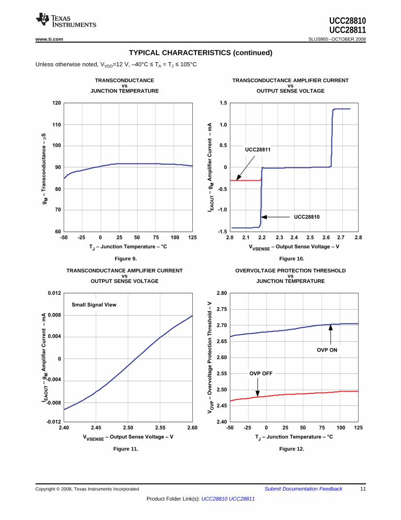
TRANSCONDUCTANCE TRANSCONDUCTANCE AMPLIFIER CURRENTvs vs
JUNCTION TEMPERATURE OUTPUT SENSE VOLTAGE
Figure 9. Figure 10.
TRANSCONDUCTANCE AMPLIFIER CURRENT OVERVOLTAGE PROTECTION THRESHOLDvs vs
OUTPUT SENSE VOLTAGE JUNCTION TEMPERATURE
Figure 11. Figure 12.
Copyright © 2008, Texas Instruments Incorporated Submit Documentation Feedback 11
Product Folder Link(s): UCC28810 UCC28811

70 432 61 5
2
0
10
-10
-8
-2
8
6
-6
-4
4
VTZE
– Transformer Zero Energy Detector Voltage – V
I TZ
E–
Tra
nsfo
rmer
Zero
En
erg
yD
ete
cto
rC
urr
en
t–
mA
125-50 50250 100-25 75
400
300
600
0
100
200
500
t RE
ST
AR
T–
Resta
rtT
ime
–m
s
TJ
– Junction Temperature – °C
4.5
5.0
3.5
1.5
2.5
2.0
3.0
4.0
5.5
CEAOUT
= 10 nF
VVSENSE
VEAOUT
t – Time – 25 ms/div
Vo
ltag
e–
V
UCC28810UCC28811SLUS865–OCTOBER 2008.............................................................................................................................................................................................. www.ti.com
TYPICAL CHARACTERISTICS (continued)Unless otherwise noted, VVDD=12 V, –40°C ≤ TA = TJ ≤ 105°C
TZE DETECTOR CURRENT RESTART TIMEvs vs
TZE DETECTOR VOLTAGE JUNCTION TEMPERATURE
Figure 13. Figure 14.
Figure 15. Voltage Amplifier Outputs
12 Submit Documentation Feedback Copyright © 2008, Texas Instruments Incorporated
Product Folder Link(s): UCC28810 UCC28811
REFERENCE DESIGNS
REFERENCE DESIGN 1
Introduction
UCC28810UCC28811
www.ti.com .............................................................................................................................................................................................. SLUS865–OCTOBER 2008
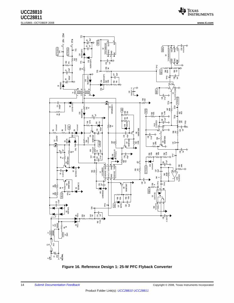
This reference design, (schematic shown in Figure 16) uses the UCC28810 LED lighting power controller in a25-W single stage triac dimmable PFC flyback converter. The input accepts a voltage range of 85 VAC to 305VAC and the output provides a regulated 750-mA current source to drive the LEDs.
Copyright © 2008, Texas Instruments Incorporated Submit Documentation Feedback 13
Product Folder Link(s): UCC28810 UCC28811
TP13
REF5
TP11
VB
IAS
TP3
VDD
REF5
REF5
REF5
J4J3J2J1
L3 33uH
11.3
k
R21
R13
1MD4 RS1J
D3R
S1J
notu
sed
R40BAT54
D17VDD
TP6
1kR36
1nF
C15
BZX84
C12
D8
Q2
MM
BT39
04
R6 1k
ST
RIN
G+
notu
sed
D19
330
R33
JP1
180k
R20
TP17
249k
R37
C13
22uF1nF
C5
330
R49
Q8
MM
BT39
06
+C14
100u
F
D9 notu
sed
R8 notu
sed
VDD
365k
R47
TP18
TP19
REF5
R39
100k
1uF
C10
MU
RA12
0T3
D10
15k
R1
1000pF
,Y1
C21
TP9
1nF
C29
TP15
10nF
C17
TP8
+C6 10
00uF
TP4
51k
R10
TP1
TP5
+
47nF
C1
0.0
47uF
C26
1mH
L2
R17
1M
10uF
C20
TP10
C2 0.1u
F
C22 1nF
Q6
MM
BT29
07 TP14
499k
R3
249k
R48
10nF
C27
C28
0.1u
F
C30 1uF
R9 1k
notu
sed
R19
1nF
C32
47pF
C19
R24 10
R4 notu
sed
R51
49.920k
R29
5.76
k
R44
R15 10
0.1u
F
C25
240u
HT1
D12
MU
RA12
0T3
1uF
C16
R12
0.39
+C9 33
uF
VB
IAS
TP20
REF5
TP12
ST
RIN
G-
ST
RIN
G+
R5 33
F1 1A
24.9
k
R45
R35
100k
100k
R38
BY
S10-2
5D16
R26
100k
C11 1nF
0.1u
F
C12TP7
LM40
40D
20
VR
1
0.0
47uF
C4
Q3
MM
BT39
041kR7
ST
RIN
G-
C31 1uF
TP16
5
2
3 41
U5
TLV
3701C
DB
V
C23
0.1u
F
R32
4.99
k
R25
10k
R27
22k
15V
D15
R14
notu
sed
D1
MU
R84
0G10
00pFC3
R46
200k 10k
R52
VDD CT
SN
S
RST
MR
GN
D
U6
TP
S3808G
50D
BV
R
MU
RA12
0T3
D11
20R16
TP2
2.2u
F
C7
FH
1
L12.
2mH
U4:
B
TLV
272C
D
C18
47pF
100
R28
R30
100k
0R41
R42
13.3
k
U3
CN
Y17
-3S
VS
EN
SE
EA
OU
T
VIN
S
ISE
NS
ETZE
GN
D
GD
RV
VDD
U1
UC
C28
810D
D2K
BP
06G
BZ
X84C
18T
D7
499kR2 R11
1k
R50
20kC24
0.1u
F
D18
BAS16
SPA06
N80
C3
Q5
Q9
MM
BT39
04
R22
100k
10k
R31
R34
0.62
R43 1k
U4:
ATLV
272C
D
BAV70
D5
D6
US
1M
-13-F
Q4
MM
BTA06
3.01
k
R18
notu
sed
C33
R23
1MO
UT IN
FB/N
C
NCGN
D
U2
TPS71
550D
CKR
C8 1uF
MU
RA12
0T3
D13
D14
MU
RA12
0T3
MM
BT39
04
Q7
2SK37
67
Q1
UCC28810UCC28811SLUS865–OCTOBER 2008.............................................................................................................................................................................................. www.ti.com
Figure 16. Reference Design 1: 25-W PFC Flyback Converter
14 Submit Documentation Feedback Copyright © 2008, Texas Instruments Incorporated
Product Folder Link(s): UCC28810 UCC28811

THEORY OF OPERATION
+
UCC28810UCC28811
www.ti.com .............................................................................................................................................................................................. SLUS865–OCTOBER 2008
Transition Mode OperationWhen the primary MOSFET switch is turned on, the drain current ramps from zero to a peak value determined bythe current reference generator output, which is the combination of the EAOUT pin voltage and the AC linevoltage waveform applied to the VINS pin. The EAOUT pin sets the power level to be transferred to thesecondary over the half sinewave cycle, and the current reference generator forces the peak switch current totrack the input line voltage to improve the power factor.
When the main switch is turned off, the peak current in the flyback inductor is transferred to the secondary sideand flows through the output diode to the output capacitors. This current drops to zero at the rate determined bythe output winding inductance and the output capacitor voltage. When the output current reaches zero, the diodestops conducting, and all of the output windings and the drain of the MOSFET ring down towards ground. Thisringing is detected on the primary side by the TZE pin of the UCC28810 as it rings below approximately 1.4 V onthe bias winding. This triggers the next switch-on pulse to start very near the valley of the ringing waveform onthe drain of the FET, which lowers the switching losses due to COSS and reduces EMI generated by the turn onof the FET
Input Filter Damping NetworkOffline flyback converters typically need common mode and differential mode input EMI filters to meet EMIspecifications. When a triac dimmer is used with a typical L-C EMI filter, the sharp turn on edge that is generatedby the triac phase control causes the LC filter to ring back and set up an oscillation between the triac and the L-Cfilter. For this reason, the differential part of the filter is damped with a R-L network across the inductor. This canalso be accomplished with an R-C damping network across the capacitor. L3 and R5 are the dampingcomponents in the schematic shown in Figure 17.
Figure 17. Input Filter Damping Network
Copyright © 2008, Texas Instruments Incorporated Submit Documentation Feedback 15
Product Folder Link(s): UCC28810 UCC28811
UCC28810UCC28811SLUS865–OCTOBER 2008.............................................................................................................................................................................................. www.ti.com
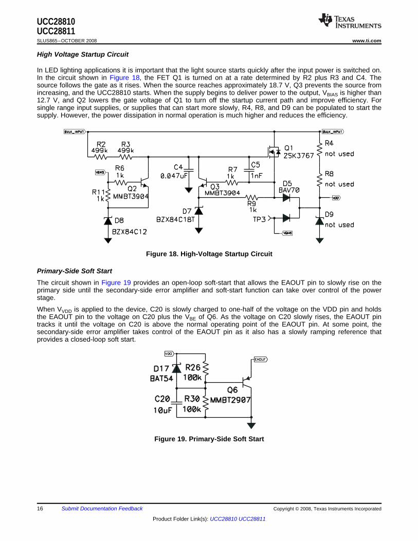
High Voltage Startup Circuit
In LED lighting applications it is important that the light source starts quickly after the input power is switched on.In the circuit shown in Figure 18, the FET Q1 is turned on at a rate determined by R2 plus R3 and C4. Thesource follows the gate as it rises. When the source reaches approximately 18.7 V, Q3 prevents the source fromincreasing, and the UCC28810 starts. When the supply begins to deliver power to the output, VBIAS is higher than12.7 V, and Q2 lowers the gate voltage of Q1 to turn off the startup current path and improve efficiency. Forsingle range input supplies, or supplies that can start more slowly, R4, R8, and D9 can be populated to start thesupply. However, the power dissipation in normal operation is much higher and reduces the efficiency.
Figure 18. High-Voltage Startup Circuit
Primary-Side Soft StartThe circuit shown in Figure 19 provides an open-loop soft-start that allows the EAOUT pin to slowly rise on theprimary side until the secondary-side error amplifier and soft-start function can take over control of the powerstage.
When VVDD is applied to the device, C20 is slowly charged to one-half of the voltage on the VDD pin and holdsthe EAOUT pin to the voltage on C20 plus the VBE of Q6. As the voltage on C20 slowly rises, the EAOUT pintracks it until the voltage on C20 is above the normal operating point of the EAOUT pin. At some point, thesecondary-side error amplifier takes control of the EAOUT pin as it also has a slowly ramping reference thatprovides a closed-loop soft start.
Figure 19. Primary-Side Soft Start
16 Submit Documentation Feedback Copyright © 2008, Texas Instruments Incorporated
Product Folder Link(s): UCC28810 UCC28811

+
UCC28810UCC28811
www.ti.com .............................................................................................................................................................................................. SLUS865–OCTOBER 2008
Primary-Side Bias RegulatorThe bias for the UCC28810 device is provided by a winding on the flyback inductor that is well coupled to theoutput winding. When the LED string voltage varies due to dimming or different configurations of LED strings, aprimary-side bias regulator formed by D15, R18, and Q4 is needed to limit the range of voltage that is applied tothe UCC28810. If dimming is not used, and the LED string forward voltage is well known, then the bias regulatorcan be removed and R14 can be populated to connect the winding voltage directly to the input supply of thedevice.
Figure 20. Primary Side Bias Regulator
Copyright © 2008, Texas Instruments Incorporated Submit Documentation Feedback 17
Product Folder Link(s): UCC28810 UCC28811

UCC28810UCC28811SLUS865–OCTOBER 2008.............................................................................................................................................................................................. www.ti.com
Leading Edge Blanking Circuit on the TZE PinAt startup, the output voltage reflected to the bias winding is well below the 1.7-V threshold that allows the nextpulse to be triggered by TZE transitioning below 1.4 V. Leakage inductance can occur between the windingscausing a leading edge spike on the TZE pin that could potentially trigger the TZE threshold and start the nextpulse before the output winding current has reached 0 A. If this happens to several pulses in a row, the primarycurrent continues to increase cycle-by-cycle until the transformer saturates and the MOSFET passes it's safeoperating area and is destroyed. The leading edge blanking circuit shown in Figure 21, consists of a chargepump, level shift, and timed blanking pulse. When the GDRV output to the MOSFET gate switches high, C19 isdischarged to VDD through D18. When the GDRV output transitions low, the base of Q8 is pulled down, and atimer consisting of C19 and R31 is started.
For the time allowed, current set by R29 is fed through Q8 to the base of Q7, which pulls the TZE pin to GND.Because the TZE pin sources current at approximately 0.5 V, a 100-Ω resistor, R28, is used to limit the currentand to allow C18 to be pulled below the TZE clamp by saturating Q7. When the time expires (approximately 1 µsin the schematic shown in Figure 21) C18 is charged by R27 to the bias winding voltage. When this voltagecharges above 1.7 V, the PWM latch is ready to be set by the TZE pin falling below 1.4 V, and the leakageinductance spike has been effectively blanked. When the pulse width is very small, it is possible that the time setby the blanking circuit is longer than the secondary conduction time. When this happens, the next oscillation ofthe winding is detected and the valley causes the main switch to fire. If no falling edge is detected, or the TZE pinnever rises above 1.7 V, then a 400-µs timer triggers a new pulse.
Figure 21. Leading Edge Blanking Circuit on TZE
18 Submit Documentation Feedback Copyright © 2008, Texas Instruments Incorporated
Product Folder Link(s): UCC28810 UCC28811
+
OUT
IN
FB/NC
NC
GND
UCC28810UCC28811
www.ti.com .............................................................................................................................................................................................. SLUS865–OCTOBER 2008
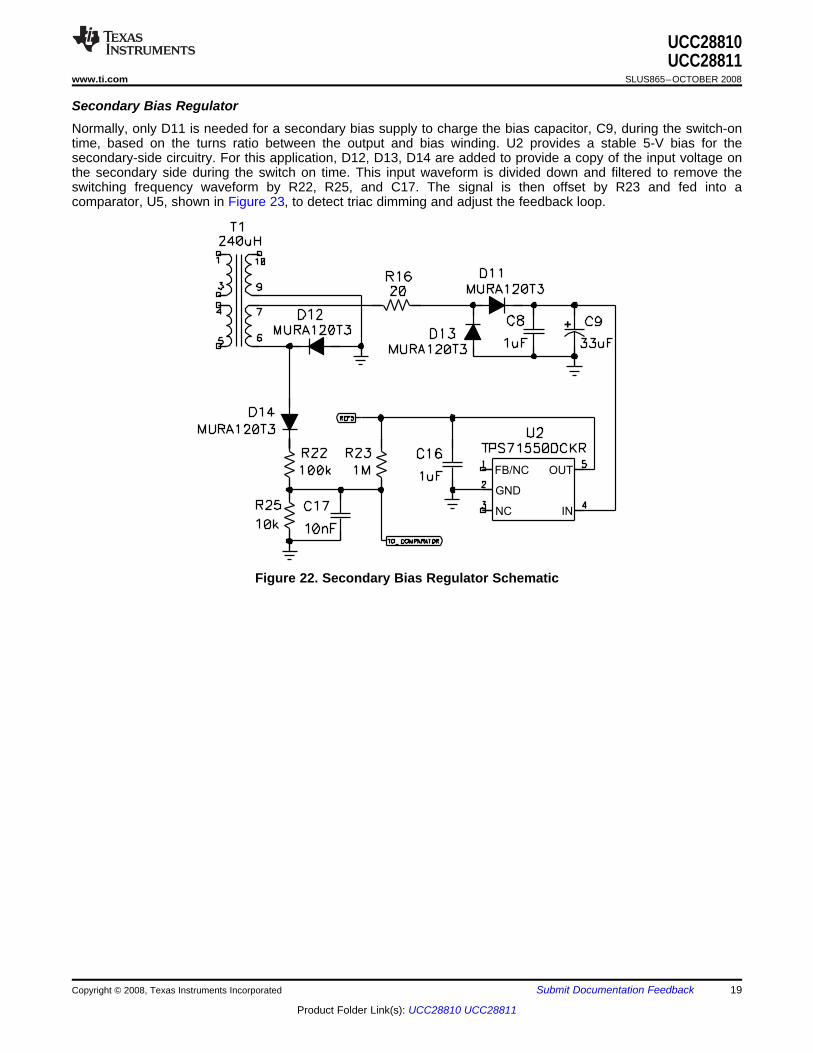
Secondary Bias RegulatorNormally, only D11 is needed for a secondary bias supply to charge the bias capacitor, C9, during the switch-ontime, based on the turns ratio between the output and bias winding. U2 provides a stable 5-V bias for thesecondary-side circuitry. For this application, D12, D13, D14 are added to provide a copy of the input voltage onthe secondary side during the switch on time. This input waveform is divided down and filtered to remove theswitching frequency waveform by R22, R25, and C17. The signal is then offset by R23 and fed into acomparator, U5, shown in Figure 23, to detect triac dimming and adjust the feedback loop.
Figure 22. Secondary Bias Regulator Schematic
Copyright © 2008, Texas Instruments Incorporated Submit Documentation Feedback 19
Product Folder Link(s): UCC28810 UCC28811

VDD
CT
SNS
RST
MR
GND
UCC28810UCC28811SLUS865–OCTOBER 2008.............................................................................................................................................................................................. www.ti.com
Triac Dimming Detection CircuitThe comparator U5 compares the copied input voltage waveform to a fixed threshold, and emits a positive pulseany time the input waveform is detected to be below the threshold. This results in a small pulse at every zerocrossing in normal operation. When a triac dimmer is used, the pulse width matches the triac dimmer off-time.This pulse sums in to the current-sense error amplifier and reduces the current regulated in the stringproportional to the off time of the triac. The programmable delay supervisory component, U6, blanks the dimmingat startup and allows the converter to start properly.
Figure 23. Triac Dimming Detection Circuit
20 Submit Documentation Feedback Copyright © 2008, Texas Instruments Incorporated
Product Folder Link(s): UCC28810 UCC28811

UCC28810UCC28811
www.ti.com .............................................................................................................................................................................................. SLUS865–OCTOBER 2008
Current Error Amplifier, Soft-Start, and Voltage Limit AmplifierComponent U4A, shown in Figure 24, fulfills the function of current error amplifier in this application.. A fixedthreshold is set by R39 and R44 and the current on the sense resistor, as represented by the signal from thetriac dimmer detection circuit, is compared to this voltage by U4A. R47 sums in the PWM dimming signal fromthe triac dimming comparator. The voltage divider formed by R37 and R48 provides a maximum output of 2.5 V,and the transistor Q9 reduces the voltage at the non-inverting input of the TLV272 to regulate the current in theLED string.
When the supply is starting up, C30 and C31 provide a soft start set by the divider resistance and capacitancevalue. After the primary soft start charges up, this secondary closed-loop soft start takes control and preventsovershoot of the supply at startup. The soft-start time provided by the secondary soft start should be longer thanthe time it takes for the power stage to fully charge the output capacitors, so that overshoot does not occur.
The second comparator of the TLV272 component, shown as U4B in Figure 24, provides a voltage limit.Because the voltage at the non-inverting input of the TLV272 cannot go higher than 2.5 V, U4B can provide aneffective maximum voltage limit by increasing the LED current in the optocoupler when the voltage is movingthrough a range determined by R35, R38, and R42. The gain is set by R45, and C27 ensures stability on theamplifier. The voltage limit amplifier is not an integrator, it has a fixed gain. Two integrators in series would causestability issues due to phase shift. R41 is provided as a provision for disconnecting the current error amplifier andregulating output voltage if desired. R49 and Q9 could be depopulated, and R41 and C27 could be changed tomake a voltage error amplifier that is an integrator.
Figure 24. Current Error Amplifier, Soft-Start, and Voltage Limit Amplifier
Copyright © 2008, Texas Instruments Incorporated Submit Documentation Feedback 21
Product Folder Link(s): UCC28810 UCC28811

REFERENCE DESIGN 2
PFC Stage
R4 BE
R15
V VR7
I
-=
(1)
UCC28810UCC28811SLUS865–OCTOBER 2008.............................................................................................................................................................................................. www.ti.com
The PR788, shown in Figure 26 is a 100-W offline AC-to-DC LED current driver with power factor correction.This design is a two stage converter design with a universal input boost follower PFC stage providing a 240-V to400-V DC output and a low-side buck stage providing the current source to power the LEDs. This converter wasdesigned to support up to 30 high-brightness LEDs in series with up to 900-mA average current. The designincorporates an interface for microprocessor control to allow for shutdown into a low power mode (< 0.5 W) andPWM dimming of the LEDs.
The PFC stage is a critical conduction mode boost converter with a boost follower feature implemented. Theboost follower is set to provide a DC output of 240 VDC to 400 VDC. The lower DC output at low input voltageresults in improved efficiency at low-line conditions. The minimum regulation point was set at 240 V to allow thedesign to be scaled to power up to 50 LEDs in series.
The critical conduction mode (CRM) of operation offers advantages regarding losses over continuous conductionmode. In CRM operation, since the inductor current reaches zero just before the beginning of the next cycle, theboost diode reverse recovery loss is eliminated. Switching losses in the MOSFET are reduced as well byprogramming a small delay after the inductor current reaches 0 A until the turn on of the MOSFET on the nextcycle. The voltage across the boost inductor begins discontinuous mode self oscillation which reduces theMOSFET drain voltage at turn on, this delay is optimized to occur at the valley of the first self oscillation cycle.
In the PFC boost implementation, the controller programs the peak inductor current to twice the value of thedesired average line current. The current reference generator uses the VINS input and the EAOUT input toprogram the peak current of the boost inductor. The VINS input is a divided sample of the rectified AC inputvoltage which is determined by R9 and the sum of (R2 + R5), as shown in Figure 26.
The C6 capacitor is used for high frequency bypass and should not affect the line frequency signal on VINS. Theminimum boost output voltage is determined by the feedback divider consisting of R11 and (R13 + R15)connected to the VSENSE pin. The boost follower circuit is hown in Figure 25.The boost follower function isaccomplished by Q1 sinking current through the high side of the feedback divider (R13 + R15). The AC inputrectified voltage is filtered and divided by R1, R3, R4, and C3. Ideally the filter minimizes the line frequency rippleand generates a DC sample of the RMS input voltage. The ratio of R4 and (R1 + R3) determines the line voltagewhich Q1 begins increasing the output by sinking current thru R13 and R15. R7 is determined by1. determining the current through R13 and R15 that provides the desired increase in the boost output2. determine the voltage across R4 at high line
.
22 Submit Documentation Feedback Copyright © 2008, Texas Instruments Incorporated
Product Folder Link(s): UCC28810 UCC28811

VSENSE
EAOUT
VINS
ISENSE TZE
GND
GDRV
VDD
VAC Input
( )
OUT
IN min
1.7 VR21
P 2 2 1.2
V
@´ ´ ´
h´(2)
( ) ( )( ) ( )( )( )
2
OUT min IN min IN min
S OUTOUT min
V 2 V VL2
2 f V P
- ´ ´ h´@
´ ´ ´(3)
UCC28810UCC28811
www.ti.com .............................................................................................................................................................................................. SLUS865–OCTOBER 2008
Figure 25. Boost Follower Circuit
The voltage error amplifier compensation network is R10, C4 and C7 connected from EAOUT to GND. The goalis to provide a loop crossover frequency at 1/10 input line frequency (10 Hz) with 45° phase margin.
The current sense resistor (R21) is determined by the following equation which is based on peak inductor currentat low line, 1.7 V ISENSE threshold, and 20% margin.
The boost inductor value can be determined based on the desired minimum operating frequency which occurs atthe peak of low line input voltage.
.
Copyright © 2008, Texas Instruments Incorporated Submit Documentation Feedback 23
Product Folder Link(s): UCC28810 UCC28811

UCC28810UCC28811SLUS865–OCTOBER 2008.............................................................................................................................................................................................. www.ti.com
Figure 26. PR788 Reference Design Schematic
24 Submit Documentation Feedback Copyright © 2008, Texas Instruments Incorporated
Product Folder Link(s): UCC28810 UCC28811

Low-Side Buck Stage
( )SW minPK PK
IN OUT OUT
1f
L I L I
V V V
@æ ö æ ö´ ´
+ç ÷ ç ÷-è ø è ø (4)
UCC28810UCC28811
www.ti.com .............................................................................................................................................................................................. SLUS865–OCTOBER 2008
The LED current is provided by a low-side buck converter operating in critical conduction mode, shown inFigure 29. The buck controller is programmed to provide a peak current of two times (2 ×) the maximum averageload current of 0.9 A (nom). The critical conduction mode allows the current to reach 0 A before beginning thenext cycle. This method provides high-efficiency due to minimized voltage on the MOSFET drain at turn on.Cycle-by-cycle current control to the LEDs is also a benefit of critical conduction mode. The average current ofthe buck driver is controlled via the PWM input (J9, Pin 3).
The UCC28811 is configured to operate in peak current limit mode with the ability to shutdown and PWM controlthe buck converter with the enable function on the VSENSE pin.
The voltage divider formed by R27 and R28 from the 5.1-V zener diode (D9) provides approx 2 V to VSENSEwhich is below the internal reference and above the enable threshold. R29 and R30 is a divider which biasesVINS at approx 3 V.
The saturated EAOUT and VINS saturates the current reference generator so the UCC28811 VDRV terminationis determined by 1.7 V on ISENSE. RSENSE (R36 + R38) is determined by the current sense threshold and 2times the desired average LED current
The minimum operating frequency of a given inductor value can be determined by summing the on and off timeof the buck switch to achieve the desired peak-to-peak current.
R40 and R48 provide a small current from LED+ into the ISENSE filter to offset the change in peak current dueto the propagation delay of the ISENSE comparator. The change in di/dt from minimum to maximum VLED+ isdetermined. The delta in di/dt results in a ΔV across RSENSE (R36 + R38). R40 and 48 are sized to match this ΔVacross (R36 + R37 + R38) with the current developed by VLED+(max)–VLED+(min).
Overvoltage protection is provided to protect against open circuit loads, shown in Figure 27. The circuit providesdetection of voltage between LED+ and LED– without a current path from LED- to ground in normal operation.The trigger voltage is determined by the total zener voltage of D15 and D19, (150 V) in this example. Once thezener breakdown is exceeded, the current through R43 will forward bias the VBE of Q6. The collector voltage ofQ6 is divided down with R44 and R42 and summed into the buck shutdown through D14.
A undervoltage lockout circuit is recommended for low-side buck LED current sources operating at outputvoltages over 115 V. A simple, effective UVLO circuit is shown in Figure 28. When the 2N2222 transistor is off,the collector is pulled high which disables the buck convertor through the common shutdown path . When thetotal zener voltage is exceeded, the 2N2222 is turned on enabling the buck converter. The UVLO enable voltageshould be selected to be between the highest anticipated buck output and the minimum output voltage of thePFC boost follower.
Copyright © 2008, Texas Instruments Incorporated Submit Documentation Feedback 25
Product Folder Link(s): UCC28810 UCC28811

UCC28810UCC28811SLUS865–OCTOBER 2008.............................................................................................................................................................................................. www.ti.com
Figure 27. Low-Side Buck OV Protection Circuit Figure 28. Low-Side Buck UVLO Circuit
26 Submit Documentation Feedback Copyright © 2008, Texas Instruments Incorporated
Product Folder Link(s): UCC28810 UCC28811

UCC28810UCC28811
www.ti.com .............................................................................................................................................................................................. SLUS865–OCTOBER 2008
Figure 29. Low-Side Buck Converter Operating in CCM
Copyright © 2008, Texas Instruments Incorporated Submit Documentation Feedback 27
Product Folder Link(s): UCC28810 UCC28811

PACKAGE OPTION ADDENDUM
www.ti.com 19-Sep-2015
Addendum-Page 1
PACKAGING INFORMATION
Orderable Device Status(1)
Package Type PackageDrawing
Pins PackageQty
Eco Plan(2)
Lead/Ball Finish(6)
MSL Peak Temp(3)
Op Temp (°C) Device Marking(4/5)
Samples
UCC28810D ACTIVE SOIC D 8 75 Green (RoHS& no Sb/Br)
CU NIPDAU Level-1-260C-UNLIM -40 to 105 28810D
UCC28810DG4 ACTIVE SOIC D 8 75 Green (RoHS& no Sb/Br)
CU NIPDAU Level-1-260C-UNLIM -40 to 105 28810D
UCC28810DR ACTIVE SOIC D 8 2500 Green (RoHS& no Sb/Br)
CU NIPDAU Level-1-260C-UNLIM -40 to 105 28810D
UCC28810DRG4 ACTIVE SOIC D 8 2500 Green (RoHS& no Sb/Br)
CU NIPDAU Level-1-260C-UNLIM -40 to 105 28810D
UCC28811D ACTIVE SOIC D 8 75 Green (RoHS& no Sb/Br)
CU NIPDAU Level-1-260C-UNLIM -40 to 105 28811
UCC28811DG4 ACTIVE SOIC D 8 75 Green (RoHS& no Sb/Br)
CU NIPDAU Level-1-260C-UNLIM -40 to 105 28811
UCC28811DR ACTIVE SOIC D 8 2500 Green (RoHS& no Sb/Br)
CU NIPDAU Level-1-260C-UNLIM -40 to 105 28811
(1) The marketing status values are defined as follows:ACTIVE: Product device recommended for new designs.LIFEBUY: TI has announced that the device will be discontinued, and a lifetime-buy period is in effect.NRND: Not recommended for new designs. Device is in production to support existing customers, but TI does not recommend using this part in a new design.PREVIEW: Device has been announced but is not in production. Samples may or may not be available.OBSOLETE: TI has discontinued the production of the device.
(2) Eco Plan - The planned eco-friendly classification: Pb-Free (RoHS), Pb-Free (RoHS Exempt), or Green (RoHS & no Sb/Br) - please check http://www.ti.com/productcontent for the latest availabilityinformation and additional product content details.TBD: The Pb-Free/Green conversion plan has not been defined.Pb-Free (RoHS): TI's terms "Lead-Free" or "Pb-Free" mean semiconductor products that are compatible with the current RoHS requirements for all 6 substances, including the requirement thatlead not exceed 0.1% by weight in homogeneous materials. Where designed to be soldered at high temperatures, TI Pb-Free products are suitable for use in specified lead-free processes.Pb-Free (RoHS Exempt): This component has a RoHS exemption for either 1) lead-based flip-chip solder bumps used between the die and package, or 2) lead-based die adhesive used betweenthe die and leadframe. The component is otherwise considered Pb-Free (RoHS compatible) as defined above.Green (RoHS & no Sb/Br): TI defines "Green" to mean Pb-Free (RoHS compatible), and free of Bromine (Br) and Antimony (Sb) based flame retardants (Br or Sb do not exceed 0.1% by weightin homogeneous material)
(3) MSL, Peak Temp. - The Moisture Sensitivity Level rating according to the JEDEC industry standard classifications, and peak solder temperature.
(4) There may be additional marking, which relates to the logo, the lot trace code information, or the environmental category on the device.

PACKAGE OPTION ADDENDUM
www.ti.com 19-Sep-2015
Addendum-Page 2
(5) Multiple Device Markings will be inside parentheses. Only one Device Marking contained in parentheses and separated by a "~" will appear on a device. If a line is indented then it is a continuationof the previous line and the two combined represent the entire Device Marking for that device.
(6) Lead/Ball Finish - Orderable Devices may have multiple material finish options. Finish options are separated by a vertical ruled line. Lead/Ball Finish values may wrap to two lines if the finishvalue exceeds the maximum column width.
Important Information and Disclaimer:The information provided on this page represents TI's knowledge and belief as of the date that it is provided. TI bases its knowledge and belief on informationprovided by third parties, and makes no representation or warranty as to the accuracy of such information. Efforts are underway to better integrate information from third parties. TI has taken andcontinues to take reasonable steps to provide representative and accurate information but may not have conducted destructive testing or chemical analysis on incoming materials and chemicals.TI and TI suppliers consider certain information to be proprietary, and thus CAS numbers and other limited information may not be available for release.
In no event shall TI's liability arising out of such information exceed the total purchase price of the TI part(s) at issue in this document sold by TI to Customer on an annual basis.

TAPE AND REEL INFORMATION
*All dimensions are nominal
Device PackageType
PackageDrawing
Pins SPQ ReelDiameter
(mm)
ReelWidth
W1 (mm)
A0(mm)
B0(mm)
K0(mm)
P1(mm)
W(mm)
Pin1Quadrant
UCC28810DR SOIC D 8 2500 330.0 12.4 6.4 5.2 2.1 8.0 12.0 Q1
UCC28811DR SOIC D 8 2500 330.0 12.4 6.4 5.2 2.1 8.0 12.0 Q1
PACKAGE MATERIALS INFORMATION
www.ti.com 18-Sep-2015
Pack Materials-Page 1

*All dimensions are nominal
Device Package Type Package Drawing Pins SPQ Length (mm) Width (mm) Height (mm)
UCC28810DR SOIC D 8 2500 340.5 338.1 20.6
UCC28811DR SOIC D 8 2500 340.5 338.1 20.6
PACKAGE MATERIALS INFORMATION
www.ti.com 18-Sep-2015
Pack Materials-Page 2


IMPORTANT NOTICE
Texas Instruments Incorporated and its subsidiaries (TI) reserve the right to make corrections, enhancements, improvements and otherchanges to its semiconductor products and services per JESD46, latest issue, and to discontinue any product or service per JESD48, latestissue. Buyers should obtain the latest relevant information before placing orders and should verify that such information is current andcomplete. All semiconductor products (also referred to herein as “components”) are sold subject to TI’s terms and conditions of salesupplied at the time of order acknowledgment.TI warrants performance of its components to the specifications applicable at the time of sale, in accordance with the warranty in TI’s termsand conditions of sale of semiconductor products. Testing and other quality control techniques are used to the extent TI deems necessaryto support this warranty. Except where mandated by applicable law, testing of all parameters of each component is not necessarilyperformed.TI assumes no liability for applications assistance or the design of Buyers’ products. Buyers are responsible for their products andapplications using TI components. To minimize the risks associated with Buyers’ products and applications, Buyers should provideadequate design and operating safeguards.TI does not warrant or represent that any license, either express or implied, is granted under any patent right, copyright, mask work right, orother intellectual property right relating to any combination, machine, or process in which TI components or services are used. Informationpublished by TI regarding third-party products or services does not constitute a license to use such products or services or a warranty orendorsement thereof. Use of such information may require a license from a third party under the patents or other intellectual property of thethird party, or a license from TI under the patents or other intellectual property of TI.Reproduction of significant portions of TI information in TI data books or data sheets is permissible only if reproduction is without alterationand is accompanied by all associated warranties, conditions, limitations, and notices. TI is not responsible or liable for such altereddocumentation. Information of third parties may be subject to additional restrictions.Resale of TI components or services with statements different from or beyond the parameters stated by TI for that component or servicevoids all express and any implied warranties for the associated TI component or service and is an unfair and deceptive business practice.TI is not responsible or liable for any such statements.Buyer acknowledges and agrees that it is solely responsible for compliance with all legal, regulatory and safety-related requirementsconcerning its products, and any use of TI components in its applications, notwithstanding any applications-related information or supportthat may be provided by TI. Buyer represents and agrees that it has all the necessary expertise to create and implement safeguards whichanticipate dangerous consequences of failures, monitor failures and their consequences, lessen the likelihood of failures that might causeharm and take appropriate remedial actions. Buyer will fully indemnify TI and its representatives against any damages arising out of the useof any TI components in safety-critical applications.In some cases, TI components may be promoted specifically to facilitate safety-related applications. With such components, TI’s goal is tohelp enable customers to design and create their own end-product solutions that meet applicable functional safety standards andrequirements. Nonetheless, such components are subject to these terms.No TI components are authorized for use in FDA Class III (or similar life-critical medical equipment) unless authorized officers of the partieshave executed a special agreement specifically governing such use.Only those TI components which TI has specifically designated as military grade or “enhanced plastic” are designed and intended for use inmilitary/aerospace applications or environments. Buyer acknowledges and agrees that any military or aerospace use of TI componentswhich have not been so designated is solely at the Buyer's risk, and that Buyer is solely responsible for compliance with all legal andregulatory requirements in connection with such use.TI has specifically designated certain components as meeting ISO/TS16949 requirements, mainly for automotive use. In any case of use ofnon-designated products, TI will not be responsible for any failure to meet ISO/TS16949.
Products ApplicationsAudio www.ti.com/audio Automotive and Transportation www.ti.com/automotiveAmplifiers amplifier.ti.com Communications and Telecom www.ti.com/communicationsData Converters dataconverter.ti.com Computers and Peripherals www.ti.com/computersDLP® Products www.dlp.com Consumer Electronics www.ti.com/consumer-appsDSP dsp.ti.com Energy and Lighting www.ti.com/energyClocks and Timers www.ti.com/clocks Industrial www.ti.com/industrialInterface interface.ti.com Medical www.ti.com/medicalLogic logic.ti.com Security www.ti.com/securityPower Mgmt power.ti.com Space, Avionics and Defense www.ti.com/space-avionics-defenseMicrocontrollers microcontroller.ti.com Video and Imaging www.ti.com/videoRFID www.ti-rfid.comOMAP Applications Processors www.ti.com/omap TI E2E Community e2e.ti.comWireless Connectivity www.ti.com/wirelessconnectivity
Mailing Address: Texas Instruments, Post Office Box 655303, Dallas, Texas 75265Copyright © 2015, Texas Instruments Incorporated