leed - oxford instruments nanotechnology gmbh 2 spectaview spectaview is a user-friendly video-leed...
TRANSCRIPT

SPECTALEED
LEED / Auger
SpectaView
MCP-LEED
MBD-LEED
SPA-LEED
LEEDInstruments for
Low Energy Electron
Diffraction and AES
Omicron NanoTechnology GmbH
www.omicron.de
2 Omicron NanoTechnology GmbH
www.omicron.de
2
Electron Spectroscopy (AES). In this case, the SPECTALEED is employed as a Retarding Field Analyser (RFA) in conjunction with the DATAuger software.
SPECTALEED delivers exceptionally sharp and bright LEED pat-terns with high resolution in k-space (typical transfer width of 300 Å at 100 eV), for easy observation even under condi-tions of high ambient light.
Non-magnetic gold plated molybdenum grids provide a high transmission (82 %) and
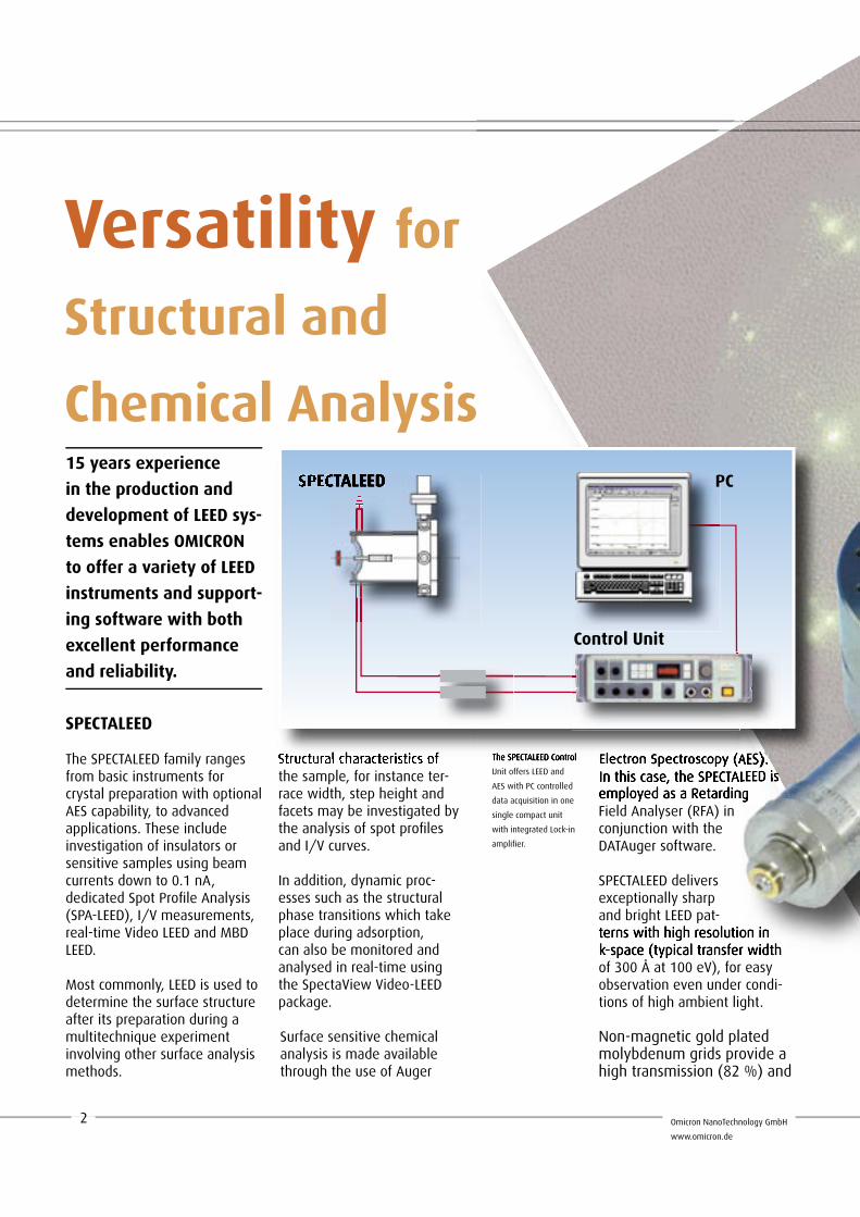
The SPECTALEED Control
Unit offers LEED and
AES with PC controlled
data acquisition in one
single compact unit
with integrated Lock-in
amplifi er.
Electron Spectroscopy (AES). In this case, the SPECTALEED is employed as a Retarding
terns with high resolution in k-space (typical transfer width
Electron Spectroscopy (AES). Electron Spectroscopy (AES). Electron Spectroscopy (AES). In this case, the SPECTALEED is In this case, the SPECTALEED is In this case, the SPECTALEED is employed as a Retarding
15 years experience
in the production and
development of LEED sys-
tems enables OMICRON
to offer a variety of LEED
instruments and support-
ing software with both
excellent performance
and reliability.
SPECTALEED
The SPECTALEED family ranges from basic instruments for crystal preparation with optional AES capability, to advanced applications. These include investigation of insulators or sensitive samples using beam currents down to 0.1 nA, dedicated Spot Profi le Analysis (SPA-LEED), I/V measurements, real-time Video LEED and MBD LEED.
Most commonly, LEED is used to determine the surface structure after its preparation during a multitechnique experiment involving other surface analysis methods.
2
Structural characteristics of the sample, for instance ter-race width, step height and facets may be investigated by the analysis of spot profi les and I/V curves.
In addition, dynamic proc-esses such as the structural phase transitions which take place during adsorption, can also be monitored and analysed in real-time using the SpectaView Video-LEED package.
Surface sensitive chemical analysis is made available through the use of Auger
Electron Spectroscopy (AES). The SPECTALEED Control Electron Spectroscopy (AES). Electron Spectroscopy (AES). Electron Spectroscopy (AES). Electron Spectroscopy (AES). Structural characteristics of
SPECTALEED
Control Unit
SPECTALEEDSPECTALEED PC
Versatility for
Structural and
Chemical Analysis
Omicron NanoTechnology GmbH
www.omicron.de
2 Omicron NanoTechnology GmbH
www.omicron.de
2
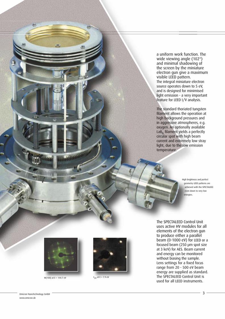
W(100) at E = 144.7 eV C60 at E = 7.9 eV
3
a uniform work function. The wide viewing angle (102°) and minimal shadowing of the screen by the miniature electron gun give a maximum visible LEED pattern.The integral miniature electron source operates down to 5 eV, and is designed for minimised light emission - a very important feature for LEED I/V analysis.
The standard thoriated tungsten fi lament allows the operation at high background pressures and in aggressive atmospheres, e.g. oxygen. An optionally available LaB6 fi lament yields a perfectly circular spot with high beam current and extremely low stray light, due to the low emission temperature.
High brightness and perfect
geometry LEED patterns are
achieved with the SPECTALEED
even down to very low
energies.
The SPECTALEED Control Unit uses active HV modules for all elements of the electron gun to produce either a parallel beam (0-1000 eV) for LEED or a focused beam (250 µm spot size at 3 keV) for AES. Beam current and energy can be monitored without biasing the sample. Lens settings for a fi xed focus range from 20 - 500 eV beam energy are supplied as standard. The SPECTALEED Control Unit is used for all LEED instruments.

Omicron NanoTechnology GmbH
www.omicron.de
2 Omicron NanoTechnology GmbH
www.omicron.de
2
MBD-LEED
The Molecular-Beam-Deposition-LEED is a new instrument for the in-situ observation of thin fi lm growth during the evaporation process. It combines 3 miniature Knudsen cells with the SPECTALEED for simultaneous and independent evaporation of up to three different materials. The Knudsen cells are integrated into the LEED optics so as to cause minimum reduction of the LEED viewing area and no disturbance of the LEED pattern.Low light emission is maintained even at the maximum evaporation temperature of approx. 700°C. The quartz glass crucibles are prealigned onto the sample and are easily exchanged and refi lled. The design geometry prevents contami-nation of the LEED grids by the evaporant.
- Temperature range 40 - 700 °C- Crucible capacity 15 mm3 (max. 50 mm3)- Evaporator control unit with up to 3 independent T-controllers, programmable via RS232
The MCP-LEED uses a
fringe-fi eld correction
plate to produce a
perfect LEED pattern
on the plane
channelplate.
MBD-LEED with
3 pre-aligned,
integrated miniature
evaporators.
1) Courtesy of: J. Vogt and H. Weiss, Univ. of Magdeburg2) Courtesy of: C. Seidel, H. Kopf and H. Fuchs, Univ. of Muenster
- Ultra low beam current 0.1 - 30 nA- Single or double channelplate- Viewing angle 70°- High stability/low noise channelplate control unit
O3(0001) at 232 eV,
beam current of 30 nA.
Al2O
beam current of 30 nA.
MCP-LEED
The highly sensitive channelplate version of the SPECTALEED reverse view LEED optics is specially designed for operation using low primary beam currents. Such low beam currents may be demanded in applications where the beam current levels experienced in standard LEED applications (typi-cally in the microampere range) may possibly lead to damage of delicate samples or cause rapid charging of insulator surfaces.With the MCP-LEED, the low beam current in the nanoampere range enables the structural study of inherently sensitive or prob-lematic samples, such as insulators or single crystals with weakly bound adsorbates, without complications caused by deterioration due to beam-induced effects.The primary beam current may be further reduced, down to the picoampere range, by means of a second channelplate.
NaCl(100) with 5nA
beam current 1)
Organic molecules (DCNQI) on
Ag(110) during deposition in UHV
at 340 K (electron energy: 14.6
eV). Spots produced by the restruc-
turing of molecules into a denser
packing are marked yellow 2).
4
Omicron NanoTechnology GmbH
www.omicron.de
2
SpectaView
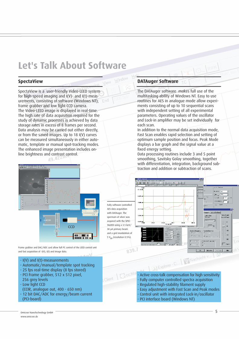
SpectaView is a user-friendly Video-LEED system for high-speed imaging and I(V)- and I(t)-meas-urements, consisting of software (Windows NT), frame grabber and low light CCD camera. The Video-LEED image is displayed in real-time. The high rate of data acquisition required for the study of dynamic processes is achieved by data storage rates in excess of 8 frames per second.Data analysis may be carried out either directly, or from the saved images. Up to 18 I(V) curves can be measured simultaneously in either auto-matic, template or manual spot-tracking modes. The enhanced image presentation includes on-line brightness and contrast control.
- I(V) and I(t)-measurements - Automatic/manual/template spot tracking - 25 fps real-time display (8 fps stored) - PCI Frame grabber, 512 x 512 pixel, 256 grey levels - Low light CCD (CCIR, analogue out, 400 - 650 nm) - 12 bit DAC/ADC for energy/beam current (PCI-board)
- Active cross-talk compensation for high sensitivity- Fully computer controlled spectra acquisition- Regulated high-stability fi lament supply- Easy adjustment with Fast Scan and Peak modes- Control unit with integrated Lock-in/oscillator- PCI interface board (Windows NT)
DATAuger Software
The DATAuger software makes full use of the multitasking ability of Windows NT. Easy to use routines for AES in analogue mode allow experi-ments consisting of up to 10 sequential scans with independent setting of all experimental parameters. Operating values of the oscillator and Lock-in amplifi er may be set individually for each scan. In addition to the normal data acquisition mode, Fast Scan enables rapid selection and setting of optimum sample position and focus. Peak Mode displays a bar graph and the signal value at a fi xed energy setting.Data processing routines include 3 and 5 point smoothing, Savitsky Golay smoothing, together with differentiation, integration, background sub-traction and addition or subtraction of scans.
Let's Talk About Software
Fully software controlled
AES data acquisition
with DATAuger. The
spectrum of silver was
acquired with the SPEC-
TALEED using a 3.5 keV/
30 µA primary beam
and a grid modulation of
5 Vpp (resolution 0.5%).
Frame grabber and DAC/ADC card allow full PC control of the LEED control unit
and fast acquisition of I(V), I(t) and image data.
CCD
5
Omicron NanoTechnology GmbH
www.omicron.de
2 Omicron NanoTechnology GmbH
SPA-LEED
Conventional LEED is most com-monly used to judge surface perfection, identify adsorbate-induced superstructures and determine the surface structure as derived from I/V curves.Spot Profi le Analysis (SPA-LEED) was pioneered by Prof. Henzler and his group at the University of Hannover. The SPA-LEED is manufactured under exclusive licence by OMICRON.
Spot Profi le Analysis is a dedicated, high perform-ance LEED application which exploits detailed structural information contained in the width and shape of the LEED spots, to show any deviation from the ideal lattice. SPA-LEED is designed to give maximum resolution in k-space, thus extend-ing the detection limit to a typical average terrace width of about 50 nm and a mosaic angle of down to 0.01°.
Applications of SPA-LEED include the classifi cation and analysis of point defects, facets, terraces, islands, steps, horizontal and vertical roughness, thermal or static disorder, domains, and phase transitions. The technique enables precise
quantitative analysis of lateral and vertical lattice constants, terrace/island size and height distribu-tions, ordering parameters in phase transitions, and diffusion barriers at step edges.
SPA-LEED can be applied in-situ during epitaxial growth processes, chemical reactions, surface diffusion, ordering transitions, reconstruction, etc. Observation of intensity modulations and spot profi le allows precise character-isation of growth processes.
With SPA-LEED the conventional LEED pattern is only visible on a part of the LEED screen, since a section of the screen area is occupied by an elec-tron multiplier positioned behind a 100 µm aper-ture. Heart of the SPA-LEED is an octopole which is used to scan the diffracted electrons relative to the SPA-LEED detector. In this way individual LEED spots can be quantitatively analysed with excel-lent sensitivity and signal-to-noise ratio.
The dynamic range is 100 times higher than in conventional LEED, and resolution in k-space, determined by the transfer width of > 100 nm, is signifi cantly improved. Thus very low concentra-tions of defects can be detected and the nature of their structure can be investigated.
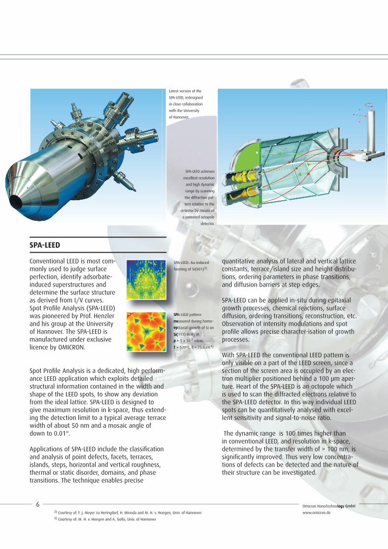
SPA-LEED achieves
excellent resolution
and high dynamic
range by scanning
the diffraction pat-
tern relative to the
detector by means of
a patented octopole
detector.
SPA-LEED: Au-induced
faceting of Si(001)3).
SPA-LEED pattern
measured during homo-
epitaxial growth of Si on
Si(111) in H2 at:
p = 5 x 10⁻⁷ mbar,
T = 520°C, E = 75.6 eV.4)
SPA-LEED pattern
measured during homo-
epitaxial growth of Si on
Si(111) in H
p = 5 x 10
T = 520°C, E = 75.6 eV.
6
Latest version of the
SPA-LEED, redesigned
in close collaboration
with the University
of Hannover.
3) Courtesy of: F. J. Meyer zu Heringdorf, H. Minoda and M. H. v. Hoegen, Univ. of Hannover4) Courtesy of: M. H. v. Hoegen and A. Golla, Univ. of Hannover

Omicron NanoTechnology GmbH
www.omicron.de
2 Omicron NanoTechnology GmbH
www.omicron.de
2Omicron NanoTechnology GmbHOmicron NanoTechnology GmbH
www.omicron.de
The SPA-LEED data acquisition and evaluation soft-ware features an easy-to- handle setup routine. Rate meter and oscilloscope functions are dis-played on the monitor, thus enabling interactive optimisation of peak shape, peak intensity, scan range and scan area. The auto-scan menu allows individual measurement routines to be defi ned and run consecutively. Electron beam energy, beam current and frequency signal from a quartz micro balance can be recorded for the control of layer growth.
The software features many useful data analysis routines including calibration of the defl ection voltage in „Percentage of Brillouin-Zone“, linear or logarithmic count rate display with scaling to the primary current or user defi ned rescaling. Zoom, smoothing, line scans, coloured 3D view, contour plots, comparison facility for two or more scans, evaluation of integral and peak intensities and FWHM of individual spots are also available.
Operation is assisted by a comprehensive manual plus an electronic Help menu.
ring" which identifi es a regular distribution of islands on the surface.
- Transfer width > 1000 Å at 95.4 eV- Beam current range 500 pA - 10 µA, LaB6 fi lament- Angular resolution better than 0.1°- Defl ection Scan ± 30°, viewing angle ± 11°- Channeltron detector for > 8 x 10⁶ cps- 16 bit DACs for defl ection, and 32 bit counter- Fixed focus range 40 - 300 eV- Fully software controlled (2 ISA PC slots, DOS)- Control unit for octopol defl ector, channeltron supply
Inte
nsity
Si/Si(111) (0,0) spot
Spot intensity oscillations and spot profi le measure-ments during epitaxial
growth processes give precise measures of the growing coverage and the
growth characteristics, e.g. increasing roughness.
The SPA-LEED is operated by the LEED control electronics in
combination with the SPA-LEED Control Unit.
SPA-LEED analysis of a diffraction spot of 5 ML Si on
H-terminated Si(111), revealing a „Henzler ring“ which
identifi es a regular distribution
of islands on the surface.
7
Coverage [Bilayers]
301-V06/10.02
Technical alterations reserved Printed by Druckerei und Verlag Klaus Koch GmbH
How to contact us
UK:
Omicron Surface Science Ltd
Tel. 01342 331000 • Fax 01342 331003
France:
Omicron Eurl
Tel. 04 42 50 68 64 • Fax 04 42 50 68 65
Italy:
Omicron NanoTechnology GmbH, Roma
Tel. (06) 35 45 85 53 • Fax (06) 35 40 38 67
Switzerland:
Omicron NanoTechnology GmbH
Tel. 055 645 5232 • Fax 055 645 5230
Sweden:
Advanced Vacuum AB
Tel. 013 21 3200 • Fax 040 41 1318
Headquarters: Omicron NanoTechnology GmbHLimburger Str. 75 • D-65232 Taunusstein • GermanyTel. +49 (0) 61 28 / 987 - 0 • Fax +49 (0) 61 28 / 987 - 185www.omicron.de or www.omicron-instruments.com
Headquarters USA:
Omicron NanoTechnology USA
Tel. (952) 746-1316 • Fax (952) 952-1320
USA (East):
Omicron NanoTechnology, E. Regional Offi ce
Tel. (724) 942-9821 • Fax (724) 942-9822
USA (West):
Omicron NanoTechnology, W. Regional Offi ce
Tel. (303) 893 2388 • Fax (303) 893 2399
Japan:
ULVAC-PHI, Inc.
Tel. 0467 85 6522 • Fax 0467 85 4411
South Korea:
Woosin Cryovac Ltd
Tel. (031) 457 5615 • Fax (031) 457 5629
Taiwan:
Omega Scientifi c Taiwan Ltd
Tel. (02) 8780-5228 • Fax (02) 8780-5225
Singapore:
Research Instruments Pte Ltd
Tel. 775-7284 • Fax 775-9228
India:
Mack International
Tel. (022) 285 52 61 • Fax (022) 285 23 26
China:
Omicron China Offi ce
Tel. (010) 82073793 • Fax (010) 82070995
Australia:
Thomson Scientifi c Instruments Pty Ltd
Tel. (03) 9663 2738 • Fax (03) 9663 3680
BRAZIL:
BOC DO BRASIL LTDA
Tel. (011) 3952 5000 • Fax (011) 3965 2766
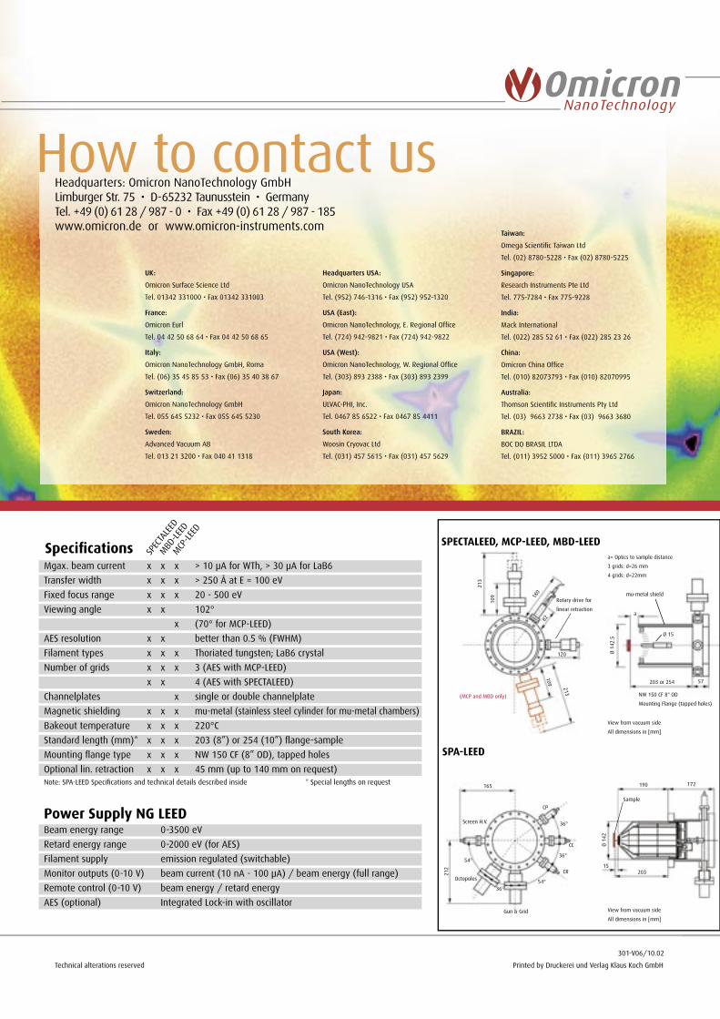
Specifi cations Mgax. beam current x x x > 10 µA for WTh, > 30 µA for LaB6
Transfer width x x x > 250 Å at E = 100 eV
Fixed focus range x x x 20 - 500 eV
Viewing angle x x 102°
x (70° for MCP-LEED)
AES resolution x x better than 0.5 % (FWHM)
Filament types x x x Thoriated tungsten; LaB6 crystal
Number of grids x x x 3 (AES with MCP-LEED)
x x 4 (AES with SPECTALEED)
Channelplates x single or double channelplate
Magnetic shielding x x x mu-metal (stainless steel cylinder for mu-metal chambers)
Bakeout temperature x x x 220°C
Standard length (mm)* x x x 203 (8”) or 254 (10”) fl ange-sample
Mounting fl ange type x x x NW 150 CF (8” OD), tapped holes
Optional lin. retraction x x x 45 mm (up to 140 mm on request)Note: SPA-LEED Specifi cations and technical details described inside * Special lengths on request
Power Supply NG LEEDBeam energy range 0-3500 eV
Retard energy range 0-2000 eV (for AES)
Filament supply emission regulated (switchable)
Monitor outputs (0-10 V) beam current (10 nA - 100 µA) / beam energy (full range)
Remote control (0-10 V) beam energy / retard energy
AES (optional) Integrated Lock-in with oscillator
MCP
-LEE
D
MBD
-LEE
D
SPEC
TALE
ED
View from vacuum side
All dimensions in [mm]
SPECTALEED, MCP-LEED, MBD-LEED
SPA-LEED
212
36°
36°
36°
54°
54°
CP
CC
CROctopoles
Screen H.V.
165
Rotary drive for
linear retraction
190 172
Sample
20315
Ø 1
42
View from vacuum side
All dimensions in [mm]
Gun & Grid
a= Optics to sample distance
3 grids: d=26 mm
4 grids: d=22mm
a
203 or 254 57
Ø 15
Ø 1
42.5
NW 150 CF 8" OD
Mounting Flange (tapped holes)
213
109
120
213
109
180
82
(MCP and MBD only)
mu-metal shield