left-handed metamaterials realized by complementary split
TRANSCRIPT
Left-handed metamaterials realized by
complementary split-ring resonators
for RF and microwave circuit
applications
A Thesis submitted to The University of Manchester for the degree
of Doctor of Philosophy
in the Faculty of Engineering and Physical Sciences
2012
Sarinya Pasakawee
Microwave and Communication Systems Research Group
School of Electrical and Electronic Engineering

2
ACKNOWLEDGEMENT
There are numerous people who I wish to thank for their assistance during this PhD
study. Firstly, I want to take this chance to give a special thanks to my supervisor,
Dr. Zhirun Hu, who has inspired this work. I also want to thank him for his
knowledge encouragement and support in both my studies and in my life. Also my
utmost gratitude to my sponsor, the Royal Thai Government, who’s funding has
supported my living and study costs.
I would also like to thank Dr. Cahyo Mustiko for his assistance discussions and
advice over my PhD both with respect to lab work and theory. Thanks are also due to
Dr. Abid Ali and Dr. Mahmoud Abdalla for their previous works without which the
inspiration for my thesis would not have been realized.
Finally, I would like to thank sincerely to my husband, Mr. Ross Allen, and the rest
of my family for their support and sacrifices for me to achieve what I have.
This thesis is an opportunity to express my thanks for all their support and
encouragement.

3
ABSTRACT
A new equivalent circuit of left-handed (LH) microstrip transmission line loaded
with Complementary split-ring resonators (CSRRs) is presented. By adding the
magnetic coupling into the equivalent circuit, the new equivalent circuit presents a
more accurate cutoff frequency than the old one. The group delay of CSRRs applied
with microstrip transmission line (TL) is also studied and analyzed into two cases
which are passive CSRRs delay line and active CSRRs delay line. In the first case,
the CSRRs TL is analyzed. The group delay can be varied and controlled via signal
frequency which does not happen in a normal TL. In the active CSRRs delay line,
the CSRRs loaded with TL is fixed. The diodes are added to the model between the
strip and CSRRs. By observing a specific frequency at 2.03GHz after bias DC
voltages from -10V to -20V, the group delay can be moved from 0.6ns to 5.6ns.
A novel microstrip filter is presented by embedding CSRRs on the ground plane of
microstrip filter. The filter characteristic is changed from a 300MHz narrowband to a
1GHz wideband as well as suppression the occurrence of previous higher spurious
frequency at 3.9GHz. Moreover, a high rejection in the lower band and a low
insertion loss of <1dB are achieved.
Finally, it is shown that CSRRs applied with planar antenna can reduce the antenna
size. The structure is formed by etching CSRRs on the ground side of the patch
antenna. The meander line part is also added on the antenna patch to tune the
operation frequency from 1.8GHz downward to 1.73GHz which can reduce the
antenna size to 74% of conventional patch antennas. By using the previous antenna
structure without meander line, this proposed antenna can be tuned for selecting the
operation frequency, by embedding a diode connected the position between patch
and ground. The results provide 350MHz tuning range with 35MHz bandwidth.

4
CONTENTS
Chapter 1: Introduction
1.1 Overview…………………………………………………………………… 17
1.2 Aim and Objectives………………………………………………………… 18
1.3 Thesis Outline……………………………………………………………… 19
1.4 References………………………………………………………………….. 22
Chapter 2: Fundamentals of Metamaterials- A Review
2.1 History……………………………………………………………………… 24
2.2 Maxwell’s Equations and Left-Handed Metamaterial Properties………….. 26
2.2.1 LHMs and its Entropy condition…………………………………… 29
2.2.2 LHMs Phenomena…………………………………………………. 31
2.2.2.1 Wave radiation in LHMs…………………………………… 31
2.2.2.2 Negative Refraction Phenomenon…………………………..35
2.2.2.3 Reversal Doppler Effect in LHMs………………………..… 37
2.3 Realization of Left-Handed Materials……………………………………… 40
2.3.1 Metal Wire Geometry……………………………………………… 41
2.3.2 Split-Ring Resonator Geometry……………………………………. 44
2.3.3 Complementary Split-Ring Resonator……………………………... 48
2.4 CSRRs applications in recently works…………………………………...... 52
2.4.1 CSRRs and its stop band characteristic…………………………….. 52
2.4.2 CSRRs and antenna applications…………………………………… 53
2.5 References………………………………………………………………….. 55
5
Chapter 3: Metamaterial Transmission Lines
Introduction…………………………………………………………………58
3.1 Dual Transmission Line Approach:
Equivalent Circuit Model and Limitations………………………………….61
3.1.1 Left-Handed Transmission Line…………………………………….65
3.1.1.1 Principle of Left-Handed Transmission Line……………….65
3.1.1.2. Equivalent Material Parameters…………………………….68
3.1.2 CRLH Theory……………………………………………………….69
3.2 CSRRs Resonant Type of MTMs TL:
Topology, its Equivalent Circuit and Synthesis…………………………… 78
3.3 Electric, Magnetic Coupling and the new Equivalent Circuit Model…….... 83
3.4 Analysing the LH operating area of CSRRs TL…………………………… 88
3.5 Conclusion…………………………………………………………………. 94
3.6 References………………………………………………………………….. 95
Chapter 4: Metamaterial Delay Line using Complementary Split
Ring Resonators
Introduction……………………………………………………………… 99
4.1 Group Delay and Dispersion on CSRRs Transmission Lines……….. … 100
4.1.1 Group Delay and Systems………………………………………… 100
4.1.2 The dispersion properties and group delay of a CSRRs TL……….101
4.2 Passive CSRRs Model and Delay Line Design Procedures……………… 103
4.3 Active CSRRs Model and Delay Line…………………………………… 112
4.4 Conclusion…………………………………………………………………116

6
4.5 References…………………………………………………………………117
Chapter 5: Filter Theory and Its Application with CSRRs
Introduction………………………………………………………………. 121
5.1 Definitions and Fundamentals of Filters…………………………………. 122
5.1.1 2-port network analysis………………………………………….... 122
5.1.2 The terminated two-port network in Z-parameters……………….. 129
5.1.3 The interconnection of two-port circuits………………………….. 130
5.2 RF& Microwave Filter Characteristics…………………………………… 132
5.3 Overview of the Design Filter……………………………………………. 133
5.3.1 The main Coupling structure……………………………………... 134
5.3.2 Electromagnetic Properties of CSRRs…………………………..... 136
5.3.3 Combination model of the microstrip coupling structure
and CSRRs………………………………………………………... 137
5.3.4 Experimental Results and Discussion…………………………….. 141
5.4 Conclusion……………………………………………………………… 144
5.5 References………………………………………………………………… 145
Chapter 6: Antenna Theory and Applications with CSRRs
Introduction………………………………………………………………. 149
6.1 Antenna Theory and its Definition……………………………………….. 150
6.1.1 Antenna Radiation and its Characteristic…………………………. 151
6.1.2 Conventional Microstrip Patch Antenna………………………….. 152
6.1.3 The Advantages and Disadvantages
of Microstrip Patch Antennas…………………………………….. 155
6.1.4 Fundamental Antenna Parameters……………………………… 157

7
6.1.5 Analysis of patch antenna………………………………………… 158
6.2 CSRRs Properties and Antenna Design……………………………… … 159
6.2.1 Meander line antenna concept………………………… ………… 161
6.2.2 Design procedures………………………………………………… 162
6.2.3 Experimental results………………………………………………. 166
6.3 A compact and tunable antenna…………………………………………... 169
6.4 Conclusion………………………………………………………………... 172
6.5 References………………………………………………………………… 173
Chapter 7: Conclusions and Future work
7.1 Conclusions……………………………………………………………….. 175
7.2 Future works……………………………………………………………. 179
List of Publications……………………………………………………… 180
Appendix…………………………………………………………………... 181

8
LIST OF FIGURES
Figure 2.1 (a)The first artificial dielectrics lenses: Lattice of conducting disks
arranged to form lens by Kock and Cohn in1948 [2.2], and (b) J.B. Pendry designed
periodic structure of negative ε and μ [2.3]………………………………............... 24
Figure 2.2 The diagrams of electric field, magnetic field, wave vector (E, H, k) and
Poynting vector (S) for electromagnetic wave propagation in right-handed and left
handed medium [2.1, 2.8]………………………………………………………….. 28
Figure 2.3 Energy flow and wave vector diagram between RH and LH interface…34
Figure 2.4 Material classifications according to є, μ pairs and η, type of waves in the
medium, and example of structures………………………………………………... 35
Figure 2.5 The refracted wave in RH and LH medium………………………….... 36
Figure 2.6 (a) Planar lenses with the interface of negative refractive index material
(arrows are the wave vector in the medium) [2.11] and (b) the negative refraction
index on RH-LH [2.12]…………………………………………………………… ..37
Figure 2.7 The Doppler effect (a) Conventional RH medium (Δω>0), and (b) LH
medium (Δω<0), respectively [2.13]……………………………………………..... 38
Figure 2.8 (a) Photo graph of the Metamaterial cube [Physic today, June 2004], and
(b) Generic view of a host medium with periodically placed structures constituting a
MTM……………………………………………………………………………….. 41
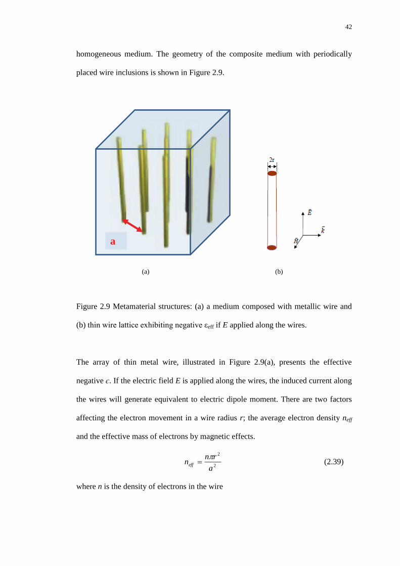
Figure 2.9 Metamaterial structures: (a) a medium composed with metallic wire and
(b) thin wire lattice exhibiting negative εeff if E applied along the wires………….. 42
Figure 2.10 Metamaterial structures: Split ring resonators lattice exhibiting negative
μeff if magnetic field H is perpendicular to the plane of the ring…………………. ..44

9
Figure 2.11 Some geometries of SRR used to realise artificial magnetic materials
[2.7]……………………………………………………………………………….. ..46
Figure 2.12 The first DNG metamaterial structures [2.5] Smith et al., 2000-2001: (a)
Mono-dimensionally DNG structure and (b) Bi-dimensionally DNG structure [2.6]
(the rings and wires are on opposite sides of the boards)………………………….. 47
Figure 2.13 Topology of CSRRs and the stack CSRRs, E is parallel to the CSRRs
plane [2.19]……………………………………………………………………….. ..48
Figure 2.14 Geometry of the CSRRs (a) with and (b) without capacitive gap
(rext=3mm, c=0.3mm, d=0.4mm on Roger/RO6006 duroid with h=1.39mm)……... 49
Figure 2.15 The simulated results of (a) scattering parameters, (b) the output phase,
and (c) the effective permittivity of a combined CSRRs structure and microstrip
line………………………………………………………………………………......50
Figure 2.16 The simulated results of (a) insertion, return loss, and (b) phase of S21
for a unit cell of CSRRs combined structure with microstrip line and a series gap
0.3mm…………………………………………………………………………….... 51
Figure 2.17 The two different sizes of CSRRs [2.21]……………………………... 52
Figure 2.18 The S-parameters of the two CSRRs sizes [2.21]…………………..... 53
Figure 2.19 (a) Photograph of the patch antenna loaded with CSRRs and (b)
simulated reflection coefficient by varying l1 (l1 is the CSRRs length)
[2.22]……………………………………………………………………………….. 53
Figure 2.20 (a) The ultra-wideband antenna with quadruple-band rejection and (b)
The measured transmission loss [2.23]…………………………………………….. 54
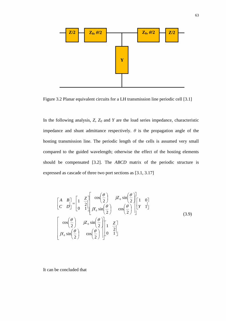
Figure 3.1 Topology of (a) SRR and (b) CSRRs with relevant dimensions…….. ..60
Figure 3.2 Planar equivalent circuits for a LH transmission line periodic cell
[3.1]……………………………………………………………………………….. ..63
10
Figure 3.3 The circuit model of a LH TL per unit length [3.1]………………….. ..65
Figure 3.4 Example of ω-β diagram in a purely LH (red) and RH (blue) TLs…... ..67
Figure 3.5 Equivalent circuit model of homogeneous CRLH TL [3.1]………….... 70
Figure 3.6 ω-β or dispersion diagram of a CRLH-TL[3.1]……………………….. 72
Figure 3.7 Simulated frequency responses of the 30-stage CRLH TL by ADS
simulation, CR=CL=1pF, LR=LL=2.5nH, respectively [3.1]……………………… ..73
Figure 3.8 Dispersion diagram of the 30-stage CRLH TL balance casein Figure
3.7………………………………………………………………………………….. 74
Figure 3.9 (a) Typical index of refraction for the balanced (green) and unbalanced
CRLH TL (red-orange), (b) the refraction index of 30-stage CRLH TL in Figure
3.7………………………………………………………………………………… ..77
Figure 3.10 Basic cell of CSRRs-based transmission line (a) and equivalent circuit
model, (b) The upper metallization is depicted in black; the slot regions of the
ground plane and depicted in grey [3.19]………………………………………….. 78
Figure 3.11 (a) The topology of CSRRs unit cell and (b) 2-cells CSRRs microstrip
TL and its magnetic field distribution at 2.4GHz……………………………….. ..84
Figure 3.12 Field variations with ring separation of the two CSRRs (a) Electric field
and (b) Magnetic field at 2.4GHz………………………………………………….. 85
Figure 3.13 Equivalent circuit model of a two adjacent-cell CSRRs TL………... ..86
Figure 3.14 (a) The S-parameters of the 2-cells CSRRs TL with cell separation of
0.2mm and (b) Smith Chart, equivalent circuit model and full wave simulation... ..87
Figure 3.15 The prototype of 4-cell CSRRs TL, (a) backside view and (b) top
view……………………………………………………………………………….... 89
Figure 3.16 The measured results of (a) S-parameters of 4 CSRRs cells and (b)
Phase of S21……………………………………………………………………….... 90

11
Figure 3.17 The S-parameters (S21 and S11) by circuit simulation and
measurement……………………………………………………………………….. 91
Figure 3.18 Dispersion diagram of 4-cell CSRRs TL…………………………… ..92
Figure 4.1 Transfer function block diagram H(jω) [4.15]……………………….. 100
Figure 4.2 (a) The topology of a unit cell CSRRs TL and Photographs of the
designed 4 –cell CSRRs TL ;(b) ground view, (c) microstrip top view………….. 104
Figure 4.3 The S-Parameters of the 4-cells CSRRs TL by both simulations and
measurement…………………………………………………………………….. 105
Figure 4.4 The group delay on passband of the 4-cells CSRRs TL by both
simulations (dot and dash blue) and measurement (solid blue) as well as a
conventional TL at length=35mm (red), respectively…………………………… 106
Figure 4.5 The dispersive delay line in a simple RF system [4.13]……………… 108
Figure 4.6 The three continuous wave (CW) output signals in Time domain of 4-
cell. CSRRs delay lines by measurement: fcw1=2.2GHz (blue), fcw2=2.3GHz (pink),
and fcw3=2.4GHz (red), respectively……………………………………………… 108
Figure 4.7 The modulated output signals with different carriers ( fc1=2.25GHz in dot
red and fc2=2.5GHz in solid blue)………………………………………………. 110
Figure 4.8 The Envelopes of RF Pulse fc1 and fc2 in time domain compared to input
after travelling through the 4-cell CSRRs by the measured S-parameters……….. 111
Figure 4.9 (a) The equivalent circuit of two adjacent CSRR cells with varactor
diodes, (b) and (c) the photographs of the fabricated 4-cells CSRRs active delay line
on both sides……………………………………………………………………. 113
Figure 4.10 The insertion response (dB) after DC bias voltages of 4-cell CSRRs
TL………………………………………………………………………………… 114

12
Figure 4.11 Measured delay time of the 4-cells active CSRRs delay line at the
frequency of 2.03GHz with different applied voltages…………………………. 115
Figure 5.1 Two-port network with the input reflection coefficient and the output
reflection coefficient [5.1]………………………………………………………... 123
Figure 5.2 Interconnection of two-port network (a) Series, (b) Parallel, and (c)
Cascade [5.26]……………………………………………………………………. 131
Figure 5.3 The transfer function of Bandpass filter……………………………… 132
Figure 5.4 The layout of a balanced load capacitance without CSRRs…………. 134
Figure 5.5 The insertion and return loss of balanced load capacitance structure
without CSRRs by HFSS simulation……………………………………………... 135
Figure 5.6 (b) The unit cell of CSRRs loaded with transmission line topology and
(b) its equivalent circuit [5.14-5.16]……………………………………………… 136
Figure 5.7 The layout of proposed filter. (a) Basic cell, (b) Topology of rectangular
CSRRs……………………………………………………………………………. 138
Figure 5.8 The current distributions of the proposed bandpass filter at (a) 0.72GHz
(no transmission) (b) 1.4GHz (centre frequency), respectively………………….. 139
Figure 5.9 The magnetic field distribution on ground plane at (a) 0.72GHz and (b)
1.4GHz, respectively…………………………………………………………….. 139
Figure 5.10 The photograph of the fabricated filter (a) Top view, (b) Bottom view.
This proposed filter is fabricated on RO3010 substrate with thickness h=1.27mm,
total dimension of the filter is 40x41.5mm2 and dielectric constant (r) =10.2…… 140
Figure 5.11 The equivalent Circuit of proposed filter…………………………… 141
Figure 5.12 The ADS simulated S-parameters (a), and (b) comparison of ADS and
HFSS simulated frequency responses on the designed filter at 0.9-1.9GHz……. 142

13
Figure 5.13 Measured and HFSS simulated frequency response on the designed
filter at 0.9-1.9GHz……………………………………………………………… 143
Figure 6.1 Antenna Radiation diagram [6.5]…………………………………….. 152
Figure 6.2 Microstrip Patch Antenna structure………………………………….. 153
Figure 6.3 The feeding methods of a microstrip antenna (a) Coaxial feed, (b) Inset-
feed, (c) Proximity-coupled feed, and (d) Aperture-coupled feed. [6.5]………… 154
Figure 6.4 Thevenin equivalent circuit of an antenna connected to a source
[6.5]………………………………………………………………………………. 157
Figure 6.5 (a) The unit cell of CSRRs TL and (b) its T-equivalent circuit……… 160
Figure 6.6 Antenna model by HFSS simulation programme……………………. 162
Figure 6.7 Layout of the meander line (4 turns), a=0.6mm and the capacitive
gap=0.2mm………………………………………………………………………. 163
Figure 6.8 The simulated return loss (S11) of each CSRR patch antenna……… 164
Figure 6.9 The simulated field distributions at resonant frequencies (a) E field of
antenna1 at 1.8GHz and (b) E field of antenna3 at 1.73GHz, while (c) H field of
antenna1 at 1.8GHz and (d) H field of antenna3 at 1.73GHz,
respectively.............................................................................................................. 165
Figure 6.10 The surface’s current distribution at 1.73GHz of antenna3 (a) on patch
(b) on ground, respectively……………………………………………………….. 166
Figure 6.11 The photos of antenna3 (a) the meander line patch with gap (b) The
CSRRs on the ground plane……………………………………………………… 167
Figure 6.12 The return loss in dB by full wave HFSS simulation and VNA
measurement of meander line loaded patch antenna with CSRRs etched on the
ground……………………………………………………………………………. 168
Figure 6.13 The simple structure of the proposed antenna with varactor diode… 169

14
Figure 6.14 The layout of tunale patch antenna (a) ground view and (b) patch
view………………………………………………………………………………. 170
Figure 6.15 The measured return loss of the tunable CSRRs patch antenna with
different DC bias voltages……………………………………………………….. 171

15
LIST OF TABLES
Table 3.1 Extracted Element Parameters for the 2-cell CSRRs TL……………… 88
Table 5.1 The overview of the relationship between two-port network parameters
and incident and reflected wave variables [5.1, 5.23, 5.24]……………………… 127
Table 5.2 Summarization of the terminated two port circuits [5.1, 5.25, 5.26]….. 129
Table 6.1 Comparison of microstrip antennas and conventional microwave
antennas…………………………………………………………………………... 156
Table 6.2 Antennas and Meander line turns……………………………………… 163

16
LIST OF ABBREVIATIONS
ADS Advanced design system
BW Bandwidth
CPW Co-planar waveguide
CRLH Composite right/left-handed
CSRR Complementary split ring resonator
DNG Double negative material
EM Electromagnetic
FBW Fractional bandwidth
HFSS High frequency structure simulator
LH Left-handed
LHM Left-handed metamaterial
MTM Metamaterial
NRI Negative refraction index
PCB Printed circuited board
PLH Purely left-handed
PRH Purely right-handed
RF Radio frequency
RH Right-handed
SNG Single negative material
SRR Split-ring resonator
TEM Transverse electromagnetic modes
TL Transmission line
TW Thin wire
VNA Vector network analyser
17
CHAPTER 1
INTRODUCTION
1.1 Overview
Electromagnetic metamaterials (MTMs) are manmade and can be treated as
homogeneous electromagnetic structures with unusual-unnatural properties [1.1].
Left-Handed (LH) MTMs have negative electric permittivity (ε) and permeability (μ)
properties simultaneously. Because LH MTMs exhibits these double negative
parameters, LH MTMs are said to have anti-parallel phase and group velocities,
therefore gives a negative refractive index (n) [1.2]. Left-handedness was theorized
first by Veselago [1.3] and was proved experimentally by Pendry [1.4] and Smith
[1.5]. Building on this initial work, LH structures can be categorized into main
configurations: thin wires (TW) and composite materials made from an array of split
ring resonators (SRRs) [1.6]; and periodically loaded transmission lines (TLs)
usually using shunt shorted inductance (stubs, meandered or spiral lines), and series
capacitances (gap or inter-digital capacitors) [1.7]. As a result of what is previously
mentioned, in the last decade, there are many new frontiers of microwave circuits
and components in the form of LH applications [1.8-1.11], for performance
enhancement, and size reduction.
Planar circuit technology is a compatible technique to fulfill a main aim in RF-
Microwave industry for making mass produced components of high frequency, and a
wide frequency operating range. However, in microstrip technology, SRRs particles
exhibit weak H-field excitation by the incident field, as in a co-planar waveguide
18
(CPW) structure. Its specific effect is not noticeable by maintaining size [1.12-1.14].
In order to overcome these limitations, a new configuration of the radial E-field,
excites the particle, and thus has been introduced [1.13-1.14]. Complementary split
ring resonators (CSRRs) are the dual form of SRRs. Since this structure is etched on
the ground plane, under the conductor strip position, and is excited by the electric
field, induced by the conductor line. This coupling can be modeled by a series,
connecting the line capacitance to the CSRRs, and therefore, due to these benefits,
CSRRs will be used for this thesis.
1.2 Aim and Objectives
The aim of this research is to use the unique properties of MTMs via CSRRs and
transmission lines to achieve both performance and size reduction in planar
microwave applications, such as transmission line, filter, and antenna.
As mentioned, there are three main objectives of this study one of the objectives is to
present a distinctive characteristic of group delay on the left handed passband of a
novel CSRRs transmission line, which can minimize the length as well as enhance
performance of the signal delay. In communication systems, signal delay can
degrade the system quality. Delay suppressions are the recommended part of
communication systems. However, this thesis presents a new method concerning the
group delay of LH passband of CSRRs transmission line. The group delay can be
managed, as a result more signals can be sent simultaneously without any concern
over interval time of each input signal.

19
Filter is a component used to select the wanted signal and suppress the unwanted
noise. The filter performance is a crucial part resulting in system quality, therefore, it
is essential to design a high performance filter which is covered all criterion of the
selectivity, high and wide rejection out-of band, spurious suppression, as well as low
insertion loss. In planar microstrip filter, the structure and length of transmission line
are related to LC parameters and resonant frequencies. CSRRs, acting as a LC
resonator, compatible in planar microstrip technology, presented a narrow rejection
band with high selectivity, therefore, with these attractive specific properties, it is the
selected particle to fulfill the planar microstrip filter criteria, as it exhibits good
functionality and size.
Antenna is the front end in transmitter and receiver part. In antenna technology, the
patch antenna size is larger when there is a lower operating frequency. Therefore,
miniaturization of microstrip antenna is another objective in this thesis. Because of
the specific permittivity characteristic of CSRRs at resonant frequency, it is again the
proper particle to apply in minimization the patch antenna.
1.3 Thesis Outline
The thesis is organized into seven chapters. Chapter 2 presents the general theory of
metamaterials by explaining the Maxwell’s equations and how they are applied. The
MTMs’ specific properties, such as negative refraction and reversal Doppler Effect,
are described. The general MTMs formed in planar technology are presented; for
example, thin wires, split ring resonators (SRRs) and its dual part called
“complementary split ring resonators (CSRRs)”. In order to make a clear point with
20
regard to MTMs, the chapter will end up with some applications of MTMs in today’s
work.
In chapter 3 the general equivalent circuit models of metamaterial on microstrip
structures are presented and analyzed, which includes the purely left-handed (LH)
structure and the composite left-right handed (CRLH) structure. The left-handed
particle structure is formed by complementary split ring resonators (CSRRs), are
analyzed. In addition, the new equivalent circuit of the left-handed particle structure
with the magnetic coupling effect between the two close rings included is also
represented, which is not appeared in the previous works. In addition, the LH
passband region of CSRRs loaded TL structure is also indicated and analyzed by its
phases and dispersion relations.
Since there is very limited work to date in the delay property on planar microstrip
circuitry using MTMs, the study of delay lines using left-handed Materials (LHMs)
dispersive properties, will be explored in chapter 4. There are two separated cases in
this chapter. The passive CSRRs delay line is first analyzed. The group delays are
studied via the displayed dispersive delayed signals, as both continuous waves
(CWs) and pulse signals. In active CSRRs delay line, the presence of varactor diodes
for a tunable structure is proposed. The group delay on a specific frequency is
studied.
In chapter 5, a new configuration of microstrip wideband passband filter is
demonstrated. The filter theory is initially presented. Then, the prototype microstrip
filter is demonstrated and analyzed by introducing the rectangular CSRRs on the
21
ground plane of this prototype structure, which results in the novel microstrip filter
characteristics being changed. The filters performance is changed from a narrow
bandpass filter to a wide bandpass filter. Other filter criteria are also displayed and
investigated. In addition, the higher spurious suppression is also presented.
In chapter 6, a criterion for ‘electrically small’ size, using the negative phase
property has been developed via antenna design. The etching of CSRRs on the group
plane part of a microstrip patch antenna is presented for specific propagation and
minimization. The meander line is another option for fulfilling further size reduction.
Furthermore, the tunable patch antenna is proposed by embedding a diode connected
between the ground and the patch side. The frequency selective antenna is proposed.
Chapter 7 describes the conclusions of this thesis and future works of the CSRRs
applications which are resultant of the conclusions that were able to come about
from the study in this thesis.

22
1.4 References
[1.1] C. Caloz and T. Itoh, Electromagnetic Metamaterials: Transmission Line
Theory and Microwave Applications, Wiley-Interscience, 2006.
[1.2] G. V. Eleftheriades, and K. G. Balmain, Negative-Refraction Metamaterials:
Fundamental Principles and Applications, John Wiley & Sons, Inc., 2005.
[1.3] V. Veselago, “The electrodynamics of substances with simultaneously
negative values of ε and μ”, Soviet Physics Uspekhi, Jan-Feb 1968, vol. 10,
no.4, pp.509-514.
[1.4] J. B. Pendry, A. J. Holden, W. J. Stewart, and I. Youngs, “Extremely low
frequency plasmons in metallic mesostructure”, Physical Review Letters, June
1996, vol. 76, no. 25, pp. 4773-4776.
[1.5] D. R. Smith, W. J. Padilla, D. C. Vier, S. C. Nemat-Nasser, and S. Schultz,
“Composite medium with simultaneously negative permeability and
permittivity”, Physical Review Letters, May 2000, vol. 84, no. 18, pp. 4184-
4187.
[1.6] M. Durán-Sindreu, A. Vélez, G. Sisó, P. Vélez, J. Selga, J. Bonache, and F.
Martín, “Recent advances in metamaterial transmission lines based on split
rings”, Proceedings of the IEEE, 2011, issue 99, pp. 1-10.
[1.7] A. Lai, T. Itoh, and C. Caloz, “Composite right/left-handed transmission line
metamaterials”, IEEE Microwave Magazine, Sept. 2004, vol. 5, no. 3, pp. 34-
50.
[1.8] F. Falcone, F. Martin, J. Bonache, R. Marqués, T. Loetegi and M. Sorolla,
“Left Handed Coplanar Waveguide Band Pass Filters Based on Bi-layer Split
Ring Resonators”, IEEE Microwave Wireless Compon. Lett., vol. 14, no. 1,
pp. 10-12, Jan. 2004.

23
[1.9] F. Falcone, F. Martín, J. Bonache, M. A. G. Laso, J. García-García, J. D.
Baena, R. Marqués, and M. Sorolla, “Stopband and band pass characteristics
in coplanar waveguides coupled to spiral resonators”, Microwave Opt.
Technol. Lett., vol. 42, pp. 386-388, Sep. 2004.
[1.10] I. Gil, J. Bonache, J. Garcia-Garcia, F. Falcone and F. Martin, “Metamaterials
in Microstrip Technology for Filter Applications”, IEEE Antennas Propag.
Int’l Symp., vol. 1A, pp. 668-671, July 2005.
[1.11] A. Ali and Z. Hu, “Compact Left-Handed Microstrip Line Based on Multiple
Layered Step Impedance Resonators”, Int. Journal of Electronics, vol. 94, no.
4, pp. 381-389, Apr. 2007.
[1.12] R. Marqué, F. Medina and R. R. –E. Idrissi, “Role of bianisotropy in negative
permeability and left handed metamaterials”, Phys. Rev. B, Condens. Matter,
vol. 65, pp. 144 441-144 446, Apr. 2002.
[1.13] F. Falcone, T. Lopetegi, J. D. Baena, R. Marqué, F. Martin, and M. Sorolla,
“Effective negative-ε stop-band microstrip lines based on complementary split
ring resonators”, IEEE Microwave Wireless Compon. Lett., vol. 14, no. 6, pp.
280-282, Jun. 2004.
[1.14] J. D. Baena, J. Bonche, F. Martin, R. Marqués, F. Falcone, T. Lopetegi, M. A.
G. Laso, J. Garcia, I. Gil, and M. Sorolla, “Equivalent-circuit models for split-
ring resonators and complementary split-ring resonators coupled to planar
transmission lines”, IEEE Trans. Microwave Theory Tech., vol. 53, no. 4, pp.
1451-1461, Apr. 2005.

24
CHAPTER 2
FUNDAMENTALS OF METAMATERIALS - A REVIEW
2.1 History
In 1968, the theoretical verification of negative index material and left handed (LH)
phenomenon in a medium with negative permittivity (ε) and negative permeability
(μ) was postulated and pointed out by Veselago [2.1]. His research showed the
exhibition of the phase velocity direction opposite to the Poynting vector of the wave
propagation in such a medium; the occurrence of backward wave propagation.
Therefore, his study is to support the theory of negative index of refraction or the
‘left handed’. Nevertheless, the substances which have negative magnetic
permeability (μ<0) are still not done until three decades later.
(a) (b)
Figure 2.1 (a)The first artificial dielectrics lenses: Lattice of conducting disks
arranged to form lens by Kock and Cohn in1948 [2.2], and (b) J.B. Pendry designed
periodic structure of negative ε and μ [2.3].
25
The first structure that showed negative permittivity in certain frequency bands was
proposed by Pendry et al [2.3, 2.4]. Owing to the ideas of Pendry, Smith [2.5]
designed a composite medium which have both negative permittivity and
permeability. Then more studies, such as Shelby et al [2.6] designed the periodical
structures by using a split-ring resonators and wire strips, have been investigated of.
Metamaterials (MTMs), their properties, and their applications have been appeared.
The Left-Handed Materials (LHMs), Double Negative (DNG) Materials, and Single
Negative (SNG) Materials, are the example names of the above mention. However,
MTMs can be referred to many materials that provide the permittivity or
permeability less than 1.
Before study, it should be firstly clarified about the definition of MTM and its
concept. MTMs are artificial materials, consisting on sub-wavelength periodic (or
quasi-periodic) inclusions (‘atoms’) of metals and/or dielectrics, whose
electromagnetic, or optical, properties can be controlled through structuring, rather
than through composition [2.7]. Since the period is smaller than a wavelength,
effective (continuous) media properties are achieved, and it is possible to obtain
properties beyond those available in nature. For these reasons, it is necessary to
study and control these unnatural material characteristics for the specific purpose in
wireless communication systems.
26
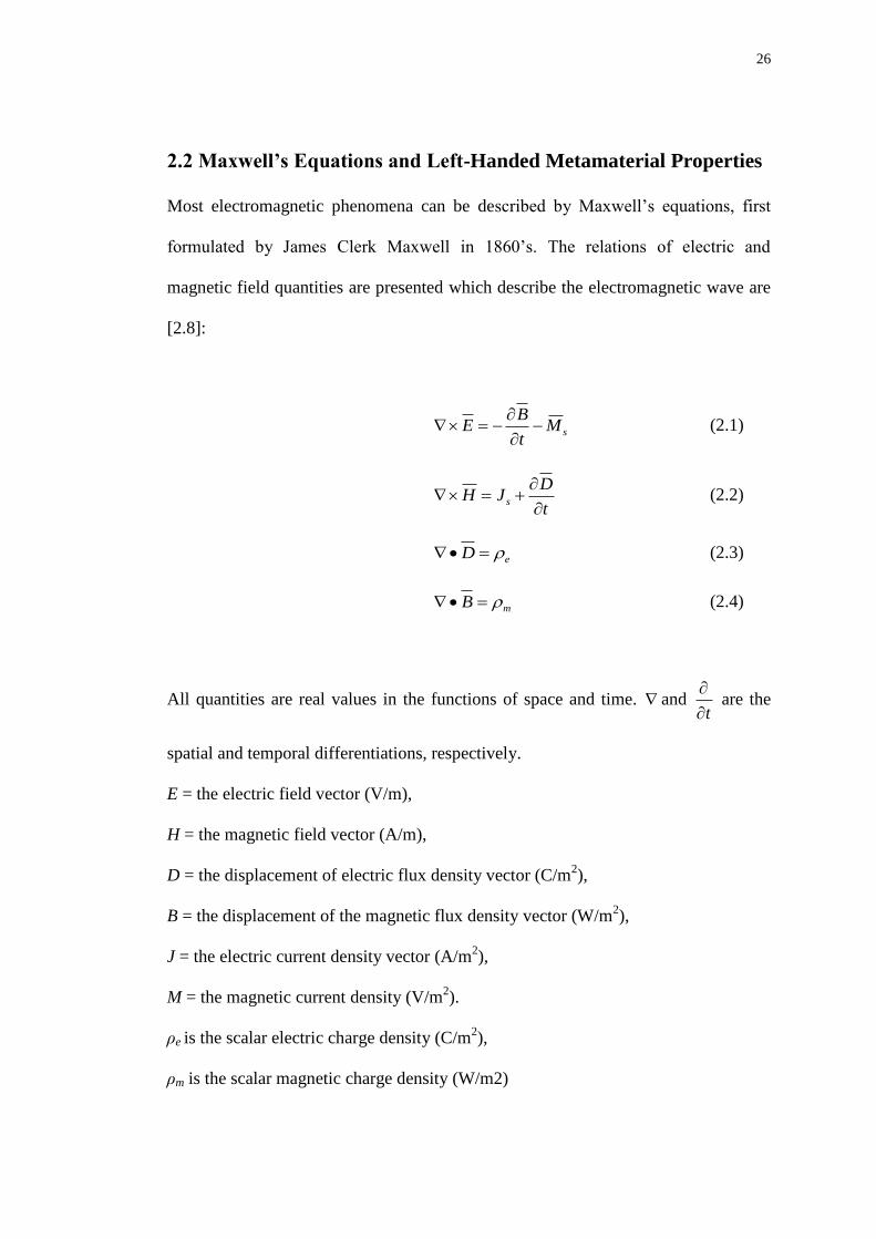
2.2 Maxwell’s Equations and Left-Handed Metamaterial Properties
Most electromagnetic phenomena can be described by Maxwell’s equations, first
formulated by James Clerk Maxwell in 1860’s. The relations of electric and
magnetic field quantities are presented which describe the electromagnetic wave are
[2.8]:
sMt
BE
(2.1)
t
DJH s
(2.2)
eD (2.3)
mB (2.4)
All quantities are real values in the functions of space and time. and t
are the
spatial and temporal differentiations, respectively.
E = the electric field vector (V/m),
H = the magnetic field vector (A/m),
D = the displacement of electric flux density vector (C/m2),
B = the displacement of the magnetic flux density vector (W/m2),
J = the electric current density vector (A/m2),
M = the magnetic current density (V/m2).
ρe is the scalar electric charge density (C/m2),
ρm is the scalar magnetic charge density (W/m2)
27
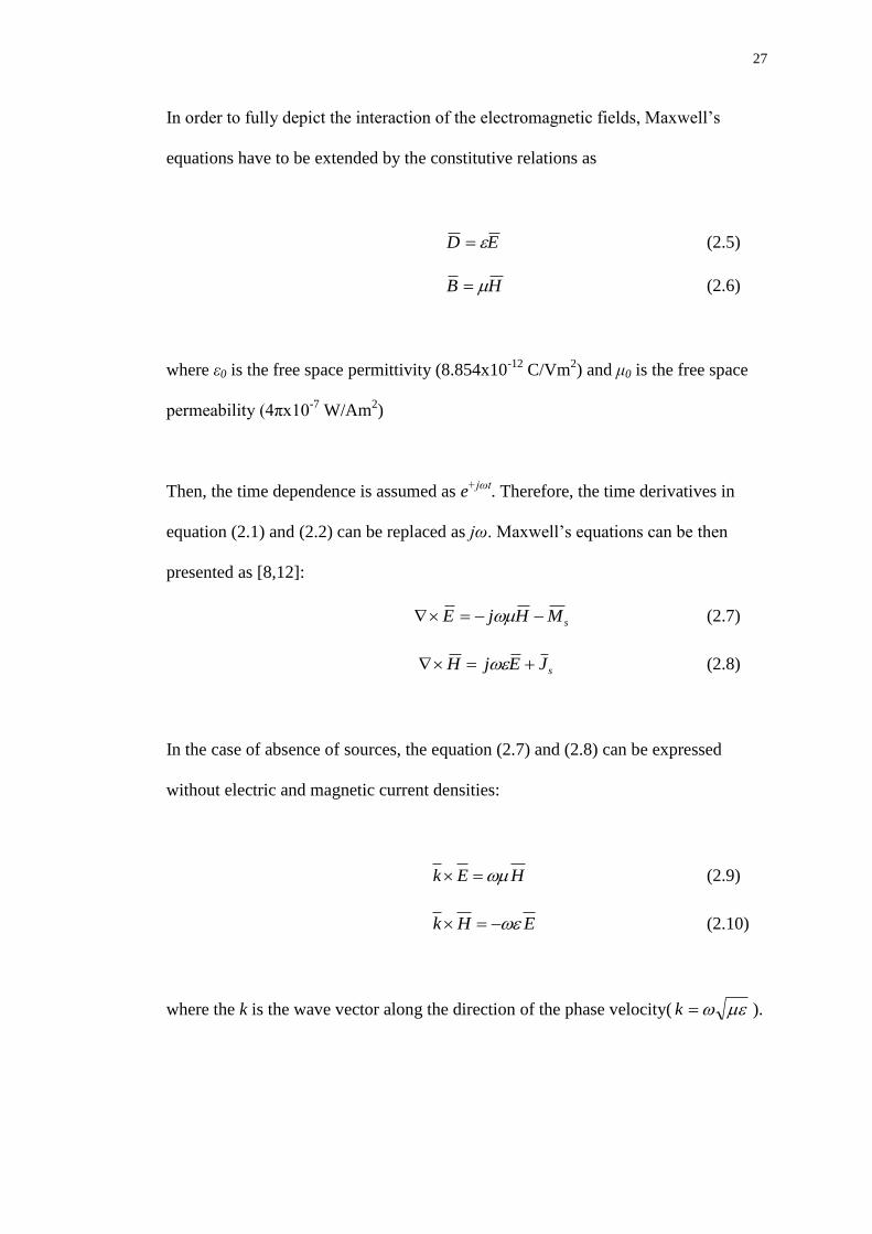
In order to fully depict the interaction of the electromagnetic fields, Maxwell’s
equations have to be extended by the constitutive relations as
ED (2.5)
HB (2.6)
where ε0 is the free space permittivity (8.854x10⁻¹²
C/Vm2) and μ0 is the free space
permeability (4πx10-7
W/Am2)
Then, the time dependence is assumed as e+jωt
. Therefore, the time derivatives in
equation (2.1) and (2.2) can be replaced as jω. Maxwell’s equations can be then
presented as [8,12]:
sMHjE (2.7)
sJEjH (2.8)
In the case of absence of sources, the equation (2.7) and (2.8) can be expressed
without electric and magnetic current densities:
HEk (2.9)
EHk (2.10)
where the k is the wave vector along the direction of the phase velocity( k ).

28
Before the study of LHMs, the right hand rule in electromagnetism will be reviewed.
When the direction of both normal E and H fields are represented by the thumb and
the index finger of the right hand respectively, placed at right angles to each other
then the middle finger placed at right angle to both the fingers gives the direction of
propagation of the wave. In nature, all electromagnetic waves such as light are
followed this rule which can be stated in mathematical form as equation (2.11):
SHE (2.11)
where E is the electric field,
H is the magnetic field and
S represents the Poynting vector and the direction of energy and wave
propagation.
Figure 2.2 The diagrams of electric field, magnetic field, wave vector (E, H, k) and
Poynting vector (S) for electromagnetic wave propagation in right-handed and left
handed medium [2.1, 2.8]
Backward Waves
k
S
E
H S
E
H
k
General Materials
(Right-handed)
Left-handed Materials
n
ε>0, μ>0 ε<0, μ<0

29
As from the previous Maxwell equations, it can be assumed that in a medium where
the permittivity and permeability is negative (LHMs), the phase velocity will be anti-
parallel to the direction of wave propagation or energy flow. In another word, the
wave has a ‘negative phase velocity’ in that medium. Even though, the direction of
energy flow is always sent from the transmitter to the receiver, the phase moves in
the opposite direction, illustrated of the S vector and the anti-parallel of k vector by
Figure 2.2.
2.2.1 LHMs and its Entropy condition
Assuming that the external supply of electromagnetic energy to the system is shut
off, the internal energy per unit volume of medium (W) is positive as illustrated in
equation (2.12-2.24).
In general medium, the internal energy per unit volume of the medium (W) by time
varying is expressed as:
dtSW . (2.12)
where S is Poynting vector in time domain with the observed distance (r ) as
),(),(),( trHtrEtrS (2.13)
Thus, the divergence of the Poynting vector is
t
DE
t
BHEHHES ..... (2.14)

30
In general medium, the relations of electric flux density (D) and electric field
intensity (E) as well as magnetic flux density (B) and magnetic field intensity (H) are
defined as
( ) ( , ) ( ') ( , ') 't
D t E r t t t E r t dt
(2.15)
t
dttrHtttrHtB ')',()'(),()( (2.16)
Then, the time varying electric field intensity at a quasi-harmonic field with median
frequency (ω0) can be presented as
*
2
1Re),( 0 EEeEtrE
tj
(2.17)
Since the following terms are zero at averaged over time
0....*
**
*
t
BH
t
BH
t
DE
t
DE (2.18)
Therefore the equation (2.14) can be written as
t
BH
t
BH
t
DE
t
DES ....
4
1. *
**
*
(2.19)
where the field components can be analyzed via Fourier series expansion to
tjet
E
d
dEj
t
D
)()( (2.20)
tjet
H
d
dHj
t
B
)()( (2.21)
Finally, the Poynting vector and the internal energy per unit volume in medium can
be reformed as

31
t
HH
d
d
t
EE
d
dS
).()().()(
4
1.
**
(2.22)
22 )()(
4
1H
d
dE
d
dW
(2.23)
As a result, the entropy condition can be written as W > 0 or it can be rewritten in the
terms of medium parameters as
0)(
d
d and 0
)(
d
d (2.24)
From equation (2.24), it is impossible that the entropy condition can be happened
while the constitutive parameters are both negative. However, this can be occurred in
frequency dependent medium which the constitutive parameters would be positive in
some frequency regions in order to compensate for their negative values. This
condition causes LHM as a causal and dispersive medium with frequency dependent
constitutive parameters.
2.2.2 LHMs Phenomena
2.2.2.1 Wave radiation in LHMs
As the wave number (k) is anti-parallel with the power flow in LHMs as well as
frequency is always a positive quantity. Therefore, the phase velocities in RH
medium are reverse compared to the LH medium. The phase velocity is defined as:
kk
Vp
~ , where
k
kk ~
(2.25)

32
The power flows of LH medium are similar to the RH medium and can be presented
as
HES (2.26)
S
sdHEP2
10 (2.27)
where S = Poynting vector
P0 = Power flow
In summary, the LH mediums provide the backward wave phenomenon due to the
reverse general direction of the phase velocity. The phase velocity is opposite of the
oriental direction while the power and group velocity are not affected [2.8].
In a homogeneous, a transverse electromagnetic (TEM) wave has a propagation
constant (β) equally to the wave number (kn) which is defined as
β= kn = ηk0 = ηω/c (2.28)
Equation (2.9) and (2.10) can be deduced to
HsE (2.29)
EsH (2.30)

33
while s is the sign that s=+1 in case of RH medium and s=-1 in case of LH medium,
respectively.
To understand a LH system, the equation of refraction index has been defined by the
square root of the constitutive parameters which are:
rr (2.31)
where η is refractive index and provides negative value in LH medium, εr is electric
permittivity of material, while μr is magnetic permeability of material
The possible real number of the signs of ε and μ are (+, +), (+, -), (-, +), and (-, -)
which lead to a double positive (DPS), single negative (SNG) or double negative
(DNG) medium, respectively. However, these negative permeability and permittivity
will not generally show the negative refractive index. However, Ziolkowski [2.9]
used the mathematics to prove the square root choice that leads to a negative index
of refraction (NRI)
It can be noted that ‘η’ can still be positive while the values of μ and ε are negative.
However, in mathematics, ‘η’ for DNG materials is negative; for example η=-1 can
be derived from phase π of both ε and μ. In negative medium, the expression of
permittivity and permeability in terms of magnitude and phase are considered as:
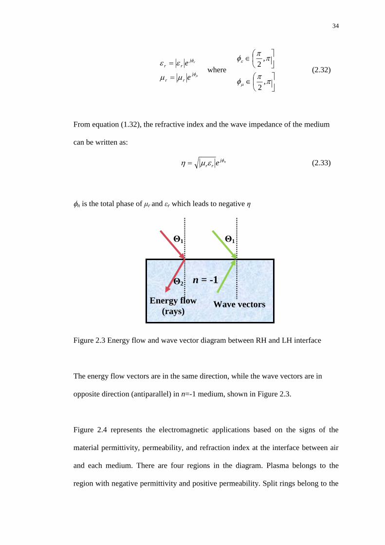
34
j
rr
j
rr
e
e
where
,2
,2
(2.32)
From equation (1.32), the refractive index and the wave impedance of the medium
can be written as:
nj
rr e (2.33)
n is the total phase of μr and εr which leads to negative η
Figure 2.3 Energy flow and wave vector diagram between RH and LH interface
The energy flow vectors are in the same direction, while the wave vectors are in
opposite direction (antiparallel) in n=-1 medium, shown in Figure 2.3.
Figure 2.4 represents the electromagnetic applications based on the signs of the
material permittivity, permeability, and refraction index at the interface between air
and each medium. There are four regions in the diagram. Plasma belongs to the
region with negative permittivity and positive permeability. Split rings belong to the
Θ1
n = -1
Energy flow
(rays) Wave vectors
Θ2
Θ1
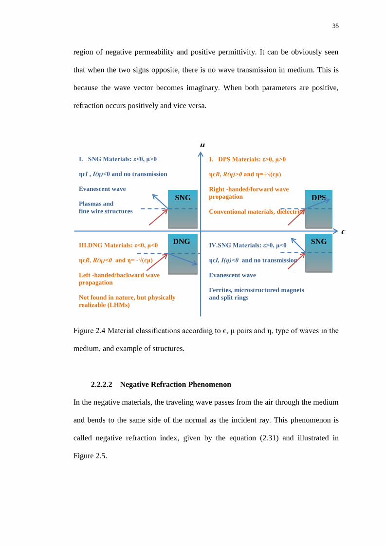
35
region of negative permeability and positive permittivity. It can be obviously seen
that when the two signs opposite, there is no wave transmission in medium. This is
because the wave vector becomes imaginary. When both parameters are positive,
refraction occurs positively and vice versa.
Figure 2.4 Material classifications according to є, μ pairs and η, type of waves in the
medium, and example of structures.
2.2.2.2 Negative Refraction Phenomenon
In the negative materials, the traveling wave passes from the air through the medium
and bends to the same side of the normal as the incident ray. This phenomenon is
called negative refraction index, given by the equation (2.31) and illustrated in
Figure 2.5.
μ
III.DNG Materials: ε<0, μ<0
ηєR, R(η)<0 and η= -√(єμ)
Left -handed/backward wave
propagation
Not found in nature, but physically
realizable (LHMs)
I. DPS Materials: ε>0, μ>0
ηєR, R(η)>0 and η=+√(єμ)
Right -handed/forward wave
propagation
Conventional materials, dielectrics
I. SNG Materials: ε<0, μ>0
ηєI , I(η)<0 and no transmission
Evanescent wave
Plasmas and
fine wire structures
IV.SNG Materials: ε>0, μ<0
ηєI, I(η)<0 and no transmission
Evanescent wave
Ferrites, microstructured magnets
and split rings
є
SNG
SNG DNG
DPS
36
Figure 2.5 The refracted wave in RH and LH medium
The Snell’s law supports the wave propagation through LHMs that bended in the
wrong way [2.10]. In Figure 2.5, the refractive index of n2’=-n2 and the wave is
refracted to the opposite side compared to the ray propagating in Right-Handed (RH)
medium. Although the wave bends the opposite direction, the Snell’s law is still been
satisfied when a negative value of n is substituted and θ2<0 into the equation,
2211 sinsin nn (2.34)
Due to its negative refractive index, the wave propagating travelling through a LHM
slab would be internally focused inside the slab and then create an image point after
leaving the slab. Pendry et al [2.11] stated the useful of this material property in
realization in ‘perfect lenses’, shown in Figure 2.6(a).
n1 n2’
Θ2 Θ1
LH
n1 n2
Θ1
Θ2 RH

37
(a)
(b)
Figure 2.6 (a) Planar lenses with the interface of negative refractive index material
(arrows are the wave vector in the medium) [2.11] and (b) the time averaged power
density of the Gaussian beam on xoy plane in lossy RH-LH (x is the distance in
metre and y is set as the axis of the wave) [2.12]
2.2.2.3 Reversal Doppler Effect in LHMs
Doppler Effect is the phenomenon that change in frequency of a wave when the
observer moving away the wave source.
Source Image 1
stfocus
38
(a) (b)
Figure 2.7 The Doppler effect (a) Conventional RH medium (Δω>0), and (b) LH
medium (Δω<0), respectively [2.13]
Consider the source P moving along z direction, while the angular frequency of the
radiated electromagnetic wave ω, illustrated in Figure 2.7. In far-field, the radiated
field can be given as [2.14]
r
etzHtzE
tj )(
),(),,(
, where krtt ),( (2.35)
whereas k refers to the wave number in medium and r is the standard radial variable
of the spherical coordinates.
In both cases, when source moves towards the positive z direction with velocity vs,
the wave position function of time is z=vst, which r=z in θ=0. Therefore, the seen
phase by observer from P to z axis is
tv
vstv
ktkvt
p
s
ss
11
(2.36)
39
Replaced vp with ω/k
Thus, the coefficient of t is the Doppler frequency (ωDoppler) defined as
Doppler , with p
s
v
vs (2.37)
In RH medium, the sign s=+1 and Δω>0, the Doppler frequency is shifted downward
when the observer is at point P and shifted upwards when the observer position is at
the right hand of moving source, displayed in Figure 2.7(a). In LH medium, sign s=-
1 and Δω<0, the phenomenon is opposite, shown in Figure 2.7(b), respectively.
Summary of the LHMs properties
There are fundamental phenomena of DNG media by Veselago in 1968 [2.1] such as
DNG medium presents the propagation of EM waves with E, H, and k in a
left-handed triad (E x H antiparallel to k).
The phase in DNG medium propagates backward to the source (backward
wave) with the phase velocity antiparallel to the group velocity.
Because of the negative permittivity and permeability, the refractive index is
negative.
The constitutive parameters of DNG medium have to be under frequency
dependent as a dispersive medium. In composite material, the permittivity
and permeability are presented as εeff and μeff, respectively.

40
2.3 Realization of Left-Handed Materials
In 1999, Pendry et al [2.3] proved that the negative effective permeability (μeff(ω))
can modify the permeability of the host substrate from an array of conducting non-
magnetic rings. The cause of bulk μeff(ω) variation for a very large positive value of
μeff(ω) at the lower resonance frequency and a significantly large negative μeff(ω) at
the higher resonance frequency is from the considerable enhancement of magnitude
of μeff(ω) when the constituent unit cells are resonantly made. Schultz et al [2.5] are
the scientists who first realized the LH materials by creating a periodical array of
interspaced conducting non-magnetic split-ring resonators and continuous wires.
Before their success of realizing the LHMs, the attempts to produce the negative
permittivity materials were made earlier by Pendry [2.16]. In order to create the
negative permittivity, a three dimensional mesh of conducting wires was used as a
structure to alter the permittivity with supporting substrate. The exhibition at the
frequency region in his experiment can show the simultaneously negative values of
both effective permeability μeff(ω) and effective permittivity εeff(ω). Then Schultz et
al [2.6] used these two concepts to create a LH structure. The wire strips and a mesh
of interspaced split-ring resonators are introduced for this achievement. The wire
strips generate ε while the split-ring resonators (SRRs) alter μ. Therefore, the
frequency dependent negative material with both negative parameters was realized.
It should be noticed that this would only happen under the condition that the size of
unit cell is considerably smaller than the smallest operation wavelength. As a result,
these periodic structures can give a uniform isotropic alteration of the base material
properties. In order to consider the actually effective parameters of a homogeneous
medium, the constraint of the wave on a unit cell dimension is analyzed.
41
For a typical electromagnetic wave of frequency (ω), the characteristic dimension of
the structure (a) should be in the condition as follow [2.3]:
a « λ = 2πcoω-1
(2.38)
Figure 2.8 shows a genetic view of the periodical structure that gives an effective
bulk permittivity and permeability for MTMs.
(a) (b)
Figure 2.8 (a) Photograph of the Metamaterial cube [Physic today, June 2004], and
(b) Generic view of a host medium with periodically placed structures constituting a
MTM.
2.3.1 Metal Wire Geometry
Pendry 1998 [2.16, 2.17] applied the individual properties of thin metallic wires
which can alter the effective permittivity of the host medium when excited
appropriately. His evaluation used a long metallic cylinder embedded in a
λg>>a
Medium with μeff, εeff
a
42
homogeneous medium. The geometry of the composite medium with periodically
placed wire inclusions is shown in Figure 2.9.
(a) (b)
Figure 2.9 Metamaterial structures: (a) a medium composed with metallic wire and
(b) thin wire lattice exhibiting negative εeff if E applied along the wires.
The array of thin metal wire, illustrated in Figure 2.9(a), presents the effective
negative є. If the electric field E is applied along the wires, the induced current along
the wires will generate equivalent to electric dipole moment. There are two factors
affecting the electron movement in a wire radius r; the average electron density neff
and the effective mass of electrons by magnetic effects.
2
2
a
rnneff
(2.39)
where n is the density of electrons in the wire
a
43
From Ampere’s law, a current flowing through a wire produces a magnetic field,
where the direction of the field is depended on the direction of the current. In
addition, the presence of the magnetic field alters the momentum of electrons. The
magnetic field H(R) is defined in equation (2.40) which is equivalent to the
momentum per unit length of wire as
R
nver
R
IRH
22)(
2
(2.40)
where I = the current flow through the wire
R = the distance from the wire
Then, the effective mass of an electron meff is expressed as
r
anremeff ln
2
22
0 (2.41)
where e = the electron charge
v = the average electron velocity
It is noticed from equation (2.40) and (2.41) that the bigger radius of the wire the
more effective mass of the electrons. This observation is later investigated in the
plasma frequency (ωp). Plasma frequency is the fundamental oscillation frequency of
the electrons while returning to the equilibrium position, termed as
r
aa
c
m
en
eff
eff
p
ln
2
2
2
0
0
2
2
(2.42)
where c0 is the speed of light in a vacuum.

44
In equation (2.42), it is noticed that decreasing the effective mass provides a large
shift in the plasma frequency. Moreover, in order to maintain the wire array as a
homogenous material, the wire radius must keep small as compared to the lattice
dimension (a). Therefore, the effective ε of the composite medium can be evaluated
from an effective homogeneous medium. In lossless metal, the plasmonic-type
permittivity is derived as
2
2
1
p
eff (2.43)
From equation (2.43), it has been appeared that the permittivity is negative when
ω<ωp. Since there is no magnetic material employed and no magnetic dipole
moment is created, the permeability is simply μ=μ0 for all frequencies.
2.3.2 Split-Ring Resonator Geometry
Because the specific property of SRRs embedded in a host medium can give the bulk
composite permeability and become negative in a certain frequency band, the study
of the region above the SRR resonant frequency has been widely observed.
Figure 2.10 Metamaterial structures: Split ring resonators lattice exhibiting negative
μeff if magnetic field H is perpendicular to the plane of the ring.
a H
E
k

45
While applying the magnetic field H perpendicular to the plane of the ring, the
induced currents then are generated around the ring equivalent to the appearance of
the magnetic dipole moments [2.3]. The permeability frequency function is formed
as
j
F
m
eff
2
0
2
2
1)( (2.44)
where ω0m is the resonant frequency in GHz range given by
d
wr
acm 30
2ln
3
(2.45)
F is the filling fraction of the SRR, while ς is the damping factor due to metal loss,
these parameters are expressed as
2
a
rF and
0
'2
r
aR (2.46)
whereas r = inner radius of the smaller ring
w = the width of the ring
d = the radial spacing between the inner and outer rings
R’ = the metal resistance per unit length.

46
Figure 2.11 some geometries of SRR used to realise artificial magnetic materials
[2.7]
The SRR structure has a magnetic response due to the presence of artificial magnetic
dipole moments by the ring resonator. At a resonant frequency range, these artificial
magnetic dipole moments are larger than the applied field which leads to the
presence of the real part of negative effective permeability, Re (μeff). In lossless case
(ς=0), the range around the resonant frequency providing negative permeability is
under the condition asF
m
pm
1
0
0
, where ωp is the plasma frequency of
the SRR particle. In other words, in the medium the discontinuity of the dispersion
relation of the permeability is occurred between ω0m and ωp because of the negative
μeff at that frequency range.
The introduction of capacitive elements that enhances the magnetic effect is
produced by the splits of rings. The strong capacitance between the two concentric
rings helps the flow of current along the SRR configuration. Since in the SRR the
capacitive and inductive effects nullify, the μeff has a resonant form. At resonant
frequency, owing to the capacitive effects due to the gap interacts with the inherent

47
inductance of the structure; the electromagnetic energy is shared between the
external magnetic field and the electrostatic fields within the capacitive structure.
Therefore, normally the experiments are focused on a certain frequency band which
is around and above the resonance frequency in order to get the negative effective
permeability [2.18].
Depicted in Figure 2.12, is the first LHM prototype designed by Smith et. al. [2.5].
In this work, the combined particles of the thin wire structure and SRR structure
appeared an overlapping frequency range that have both negative permittivity and
permeability. After applying an electromagnetic wave through this composite
structure, the pass band is presented at the frequency range of interest that the
constitutive parameters are simultaneously negative.
(a) (b)
Figure 2.12 the first DNG metamaterial structures [2.5] Smith et al., 2000-2001: (a)
Mono-dimensionally DNG structure and (b) Bi-dimensionally DNG structure [2.6]
(the rings and wires are on opposite sides of the boards)

48
2.3.3 Complementary Split-Ring Resonator
Figure 2.13 Topology of CSRRs and the stack CSRRs, E is parallel to the CSRRs
plane [2.19].
In 2004, CSRRs are firstly introduced by Falcone et al.[2.20]. The CSRRs, a dual
counterpart of SRRs or sometimes called ‘slotted split-ring resonator’, are comprised
of slots which is the same dimensions as the corresponding SRR. By the principle of
duality, the CSRRs properties are in dual relation of the SRRs properties. The SRRs
behave as a magnetic point dipole, whereas the CSRRs present an electric point
dipole with negative polarization. In CSRRs, the E field is applied parallel to the
CSRRs plane in order to generate a strong electric dipole which affects the CSRRs
resonant frequency [2.15]. The CSRRs, as shown in Figure 2.13, r can be used to
obtain the effective permittivity of a bulk medium. Both SRRs and CSRRs present
approximately the same resonant frequency due to their shared dimensions.
The CSRRs can be formed in planar transmission media by etching these resonators
in the ground plane of the microstrip. An example of this structure is demonstrated in
Figure 2.14(a). The HFSS simulation is used for design. The 50Ω line is chosen to
49
match the port impedance. This CSRRs structure provides the inhibition of signal
propagation at a resonance frequency as a narrow band.
(a) (b)
Figure 2.14 Geometry of the CSRRs (a) with and (b) without capacitive gap
(rext=3mm, c=0.3mm, d=0.4mm on Roger/RO6006 duroid with εr=6.15 and
h=1.39mm)
Considering on Figure 2.15(a) and (b), at the resonant frequency, the dip in
transmission coefficient is displayed at 3.52GHz under the sudden change of phase
to zero degree. At the frequency band above its resonant frequency, the CSRRs
proposes a negative effective permittivity in real part (unlike SRRs), whereas
exhibits positive effective permittivity at frequency band below the resonant
frequency, demonstrated in Figure 2.15(c).

50
(a)
1.00 2.00 3.00 4.00 5.00 6.00 7.00Frequency [GHz]
-175.00
-150.00
-125.00
-100.00
-75.00
-50.00
-25.00
0.00
ph
as
e S
21
[d
eg
]
SAS IP, Inc. HFSSDesign1XY Plot 3 ANSOFT
(b)
(c)
Figure 2.15 The simulated results of (a) scattering parameters, (b) the output phase,
and (c) the effective permittivity of a combined CSRRs structure and microstrip line
1.00 2.00 3.00 4.00 5.00 6.00 7.00Frequency [GHz]
-40.00
-35.00
-30.00
-25.00
-20.00
-15.00
-10.00
-5.00
0.00
S11
an
d S
21(d
B)
SAS IP, Inc. HFSSDesign1XY Plot 1 ANSOFT
S21
S11
51
Since the E field excitation in the CSRRs configuration is better matched in
microstrip transmission line, CSRRs is widely used for applying to the artificial LH
transmission lines. This structure is consisted of a microstrip line section with a
series capacitive gap etched in the conductor strip and loaded with CSRRs which
etched in the ground plane. The unit cell CSRRs transmission line is shown in Figure
2.14(b). In a composite CSRRs transmission line, these capacitive gaps need to be
etched periodically on the microstrip line to nullify the tank inductance and obtain
LH wave propagation.
(a)
1.00 2.00 3.00 4.00 5.00 6.00 7.00Frequency [GHz]
-200.00
-150.00
-100.00
-50.00
0.00
50.00
100.00
150.00
200.00
ph
as
e o
f S
21
[d
eg
]
SAS IP, Inc. HFSSDesign1XY Plot 3 ANSOFT
(b)
Figure 2.16 The simulated results of (a) insertion, return loss, and (b) phase of S21
for Figure 2.14(b) and a series gap of 0.3mm.
1.00 2.00 3.00 4.00 5.00 6.00 7.00Frequency [GHz]
-40.00
-35.00
-30.00
-25.00
-20.00
-15.00
-10.00
-5.00
0.00
S1
1 a
nd
S2
1 (
dB
)
SAS IP, Inc. HFSSDesign1XY Plot 1 ANSOFT
S21
S11

52
The LH passband range is then appeared, shown in Figure 2.16(a). At the resonant
frequency of CSRRs, the advance phase 90 degrees is obtained which is one of its
specific properties of the LHMs, illustrated in Figure 2.16(b) [2.13], [2.20] The
CSRRs analysis in terms of equivalent LC circuits will be explained in the next
chapter.
2.4 CSRRs applications in recently works
2.4.1 CSRRs and its stop band characteristic
Since CSRRs presents stop band characteristic when applied with microstrip, it has
been used to develop the filter functions. The recent work [2.21] presents a wide stop
band filter by using the co-operation of the different CSRRs dimensions. It is found
that the size of CSRRs relates to its resonant frequency in opposition. In the other
words, the small size of CSRRs is presented; the higher resonant frequency is
obtained.
Figure 2.17 the two different sizes of CSRRs [2.21]
Figure 2.17 demonstrates the two CSRRs lengths after tuning to merge their resonant
frequencies. The two resonant frequencies are now presented as one stopband,
shown in Figure 2.18.

53
Figure 2.18 the S-parameters of the two CSRRs sizes [2.21]
This application can be further applied to bandpass filter to widen the stop band as
well as increase rejection level.
2.4.2 CSRRs and antenna applications
A. Compact Patch antenna
(a) (b)
Figure 2.19 (a) Photograph of the patch antenna loaded with CSRRs and (b)
simulated reflection coefficient by varying l1 (l1 is the CSRRs length) [2.22]
The compact antenna loaded with CSRRs and reactive impedance surface (RIS) is
shown in Figure 2.19(a). The CSRRs are modeled as a shunt LC resonator which
creates resonant frequency. The photograph shows the patch size around
54
0.099λ0x0.153λ0 which is very compact. By HFSS simulation, the antenna resonant
frequency is varied inversely to the CSRRs size, illustrated in Figure 2.19(b).
B. Frequency selective antenna
(a)
(b)
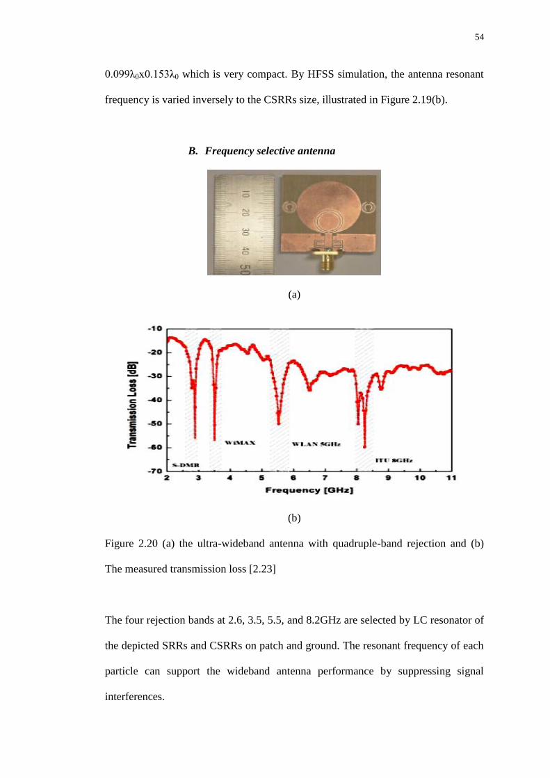
Figure 2.20 (a) the ultra-wideband antenna with quadruple-band rejection and (b)
The measured transmission loss [2.23]
The four rejection bands at 2.6, 3.5, 5.5, and 8.2GHz are selected by LC resonator of
the depicted SRRs and CSRRs on patch and ground. The resonant frequency of each
particle can support the wideband antenna performance by suppressing signal
interferences.
55
2.5 References
[2.1] V. G. Veselago, “The electrodynamics of substances with simultaneously
negative value of ε and μ”, Soviet Physics Uspekhi, vol. 10, pp. 509-514, Jan
1968.
[2.2] W.E. Kock., “Metallic delay lenses”, Bell System Technical Journal, 17:58–
82, Jan1948.
[2.3] J. B. Pendry, A. J. Holden, D. J. Robbins and W. J. Stewart, ”Magnetism
from conductors and enhanced nonlinear phenomena”, IEEE Trans.
Microwave Theory Tech, vol. 47, pp. 2075-2084, Nov 1999.
[2.4] J. B. Pendry, “Negative refraction makes a perfect lens”, Phys. Rev. Lett, vol.
85, pp. 3966-9, Oct 2000.
[2.5] D. R. Smith, W. J. Padilla, and S. Schultz, “Composite medium with
simultaneously negative permeability and permittivity”, Phys. Rev. Lett, vol.
84, pp. 4184-4187, May 2000.
[2.6] R. A. Shelby, D. R. Smith and S. Schultz, “Experimental verification of a
negative index of refraction”, Science, vol. 292, pp. 77-9, Apr 2001.
[2.7] A. F. de Baas, S. Tretyakov, P. Barois, and T. Scharf, Nanostructured
Metamaterials Exchange between experts in electromagnetics and material
science, European Union, 2010 ISBN 978-92-79-07563-6.
[2.8] D. M. Pozar, MICROWAVE ENGINEERING 3rd
edition, J. Wiley &Sons,
2005.
[2.9] R. W. Ziolkowski and E. Heyman, “Wave propagation in media having
negative permittivity and permeability”, Physical Review E, vol. 64, pp.
056625-1, Nov 2001.
56
[2.10] M. C. K. Wiltshire, “Bending of light in the wrong way”, Science 292: pp.
60-61, 2001
[2.11] J. Pendry, “Negative refraction makes perfect lens”, Physical Review Letters
Vol. 85, no. 18, pp. 3966–3969, Oct 2000.
[2.12] T. J. Cui et.al., “Study of Loss Effects on the Propagation of Propagating and
Evanescent Waves in Left-Handed Materials”, Physics Letters, pp. 484-494,
2004
[2.13] C. Caloz and T. Itoh, Electromagnetic Metamaterials Transmission Line
Theory and Microwave Applications, John Wiley & Sons, 2006.
[2.14] J. D. Kraus and R. J. Marhefka, Antennas 3rd
edition, McGraw Hill, 2001
ISBN: 007123201X.
[2.15] J. D. Baena, J. Bonache, F. Martin, and T. Lopetegi, “Equivalent-circuit
models for split-ring resonators and complementary split-ring resonators
coupled to planar transmission lines”, IEEE Trans. Microwave Theory Tech.,
vol. 53, pp. 1451-1460, Apr 2005.
[2.16] J. M. Pitarke, F. J. Garcia-Vidal, J. B. Pendry, “Effective electronic response
of a system of metallic cylinders”, Physical Review B, vol. 57, pp. 15261-5,
Jun 1998.
[2.17] J. B. Pendry, A. J. Holden, D. J. Robbins, and W. J. Stewart, “Low frequency
plasmons in thin wire structures”, J. Phys. Condens. Matter, vol. 10, pp.
4785-4809, 1998.
[2.18] K. Aydin and E. Ozbay ,”Identiying magnetic response of split-ring
resonators at microwave frequencies”, Opto-Electronics Review 14(3), pp.
193-199, DOI: 10.2478/s11772-006-0025-x

57
[2.19] M. Beruete, M. Aznabet, M. Navarro-Cia, and M. Sorolla, “Electroinductive
waves role in left-handed stacked complementary split rings resonators”,
Optics Express, vol. 17, no. 3, Feb 2009.
[2.20] F. Falcone, T. Lopetegi, J. D. Baena, and M. Sorolla, “Effective Negative-ε
Stropband Microstrip Lines Based on Complementary Split Ring
Resonators”, IEEE Microwave and Wireless Components Letters, vol. 14, no.
6, pp. 280-282, Jun 2004.
[2.21] P. Su, X. Q. Lin, R. Zhang, and Y. Fan, “An Improved CRLH wide-band
Filter using CSRRs with High Stop Band Rejection”, Progress In
Electromagnetics Research Letters, Vol. 32, pp. 119-127, 2012.
[2.22] Y. Dong, H. Toyao, and T. Itoh, “Design and Characterization of
Miniaturized Patch Antennas Loaded With Complementary Split-Ring
Resonators”, IEEE Transactions on Antennas and Propagation, vol. 60, no.
2, Feb 2012.
[2.23] N. –I. Jo, C. –Y. Kim, D. –O. Kim, and H. –A. Jang, “Compact Ultra-
Wideband Antenna with Quadruple-Band Rejection Characteristics Using
SRR/CSRR Structure”, Journal of Electromagnetic Waves and Applications,
vol. 26, pp. 583-592, 2012.
58
CHAPTER 3
METAMATERIAL TRANSMISSION LINES
INTRODUCTION
Metamaterial transmission lines (MTM TLs) are artificial lines where Right-Left
Handed composite parts embedded on a host such as microstrip transmission lines or
coplanar waveguides loaded with reactive elements. Their relevant characteristics in
either impedance or phase of these propagating structures can be controlled beyond
what can achieve in conventional transmission lines. These artificial lines, formerly
proposed in the early 2000’s [3.1-3.5], are inspired on MTMs which exhibits similar
properties and, in some cases, fabricated using identical constituent particles [3.6,
3.7].
MTM-TLs are artificial lines with controllable characteristics. Furthermore, these
artificial lines can be designed to exhibit LH wave propagation in certain frequency
bands. Such lines are normally implemented by means of lumped or semi-lumped
reactive elements. Since these elements are electrically small, the conditions to
achieve homogeneity can also be achieved, that is a small period compared to signal
wavelength. Only under these conditions, the terms of effective constitutive
parameters μeff and εeff are studied. However, homogeneity is not a fundamental
requirement in transmission lines. Indeed homogeneity can only be achieved in a
certain region of the allowed band [3.1].

59
From the point of view of microwave circuit design, the advantages of MTM-TLs
rely on miniaturization and on the possibility to control the dispersion diagram and
characteristic impedance, rather than on homogeneity. Thus, MTM-TLs are defined
as artificial lines, consisting on a host line loaded with reactive elements, with
controllable characteristics. Homogeneity is not considered to be a requirement for
such lines [3.8, 3.9]. Notice that according to this, there is no need for a minimum
number of unit cells to implement these artificial lines. Indeed, in most of the cases,
a single cell is considered since this reduces line dimensions, as will be shown later.
With regard to the implementation of MTM-TLs, there are two main approaches:
LC-loaded lines or dual transmission line [3.1-3.5, 3.10], and resonant type
approaches [3.6, 3.7]. In LC-loaded lines, proposed by Eleftheriades [3.2] and Caloz
[3.1], the key element to achieve left-handedness consists of a host line loaded with
series capacitances and shunt inductances. These lines can be implemented by using
lumped loading elements, or, alternatively, by means of semi-lumped planar
components such as series gaps, interdigital capacitors, grounded stubs or vias. The
Resonant type MTM-TLs can be implemented by loading a host line with SRRs and
shunt inductive elements [3.11, 3.12], or, alternatively, by loading a host line with
CSRRs and series capacitances [3.13-3.15]. Both LC-loaded lines and resonant type
MTM-TLs exhibit similar characteristics and dispersion. The simultaneously
negative values of the effective permeability and permittivity of the medium for both
types of the LH approaches occurred in an interval frequency that the reactive
elements dominate over the per-section capacitance and inductance of the line [3.1,
3.13, 3.14, 3.16]. Therefore, both line types are useful for the implementation of the
state-of-the-art microwave and millimeter wave circuits.

60
In this chapter, the CSRRs, a dual counterpart of SRRs, are formed to show a left
handedness in planar transmission media by etching these resonators in the ground
plane of the microstrip transmission line. Due to the presence of CSRRs, the
inhibition of signal propagation is acted at a resonance frequency as a narrow band.
This phenomenon interprets the negative effective permittivity of the medium. The
series capacitive gap is added to the structure in order to obtain the negative
permeability as well as a band pass with left handed wave propagation [3.13-3.15].
Figure 3.1 Topology of (a) SRR and (b) CSRRs with relevant dimensions.
Therefore, SRR and CSRRs based transmission lines act as the frequency selective
structures with electrically small unit-cell dimensions. The concentration of this
chapter is focused on the analyzing of one-dimensional CSRRs on microstrip
transmission line and its equivalent circuits as a specific performance.
(a) (b)
61
3.1 Dual Transmission Line Approach: Equivalent Circuit Model
and Limitations
Based on general transmission line concept, the fundamental electromagnetic
properties of LHMs and the physical realization of these materials are reviewed.
Because of the unavoidable RH properties on transmission line that occur naturally
in practical LHMs, the CRLH TL structure is also analyzed. The study of LH
transmission line is explained in the next topic as well as its characterization. Then
the design and implementation of the CSRRs TL and their applications are
presented.
Analysis for Periodic LH Transmission Line Model
Periodic analysis of the LH TL model was first introduced by Eleftheriades [3.2]. It
assumes that the periodic loaded elements are infinity. In this case, the dispersion
characteristics of the LH TL model can be calculated by applying the standard
periodic structure analysis for microwave periodic networks. ABCD matrix is used to
describe the transmission characteristics of a two port network through its input and
output currents [3.1, 3.17].
1
1
n
n
n
n
I
V
DC
BA
I
V (3.1)
For a wave propagating through a line, the voltage and current at the cells (n+1) and
(n) are also related as
d
nn eVV 1 (3.2)
d
nn eII 1 (3.3)
where γ is the propagation constant and it evaluated as
62
j (3.4)
where α is the attenuation constant and β is the phase propagation constant. From the
previous equations, it can concluded that
0
0
1
1
n
n
d
d
I
V
eDC
BeA
(3.5)
So, for a non-trivial solution, the characteristic equation for (3.5) is
0 BCeDeA dd (3.6)
Making use of the relation of reciprocal for any two- port passive network,
AD-BC=1 (3.7)
Substituting the previous equations, the propagation condition can be written as
DAddjdd 5.0sinsinhcoscosh (3.8)
Then to analyze the propagation of a very short LH TL model, the planar equivalent
circuit of a unit cell is introduced. The LH transmission line model has a section of a
transmission line of length d and loaded with a series impedance Z and a shunt
admittance Y. For a lossless cell the equivalent circuit is shown in Figure 3.2.
63
Figure 3.2 Planar equivalent circuits for a LH transmission line periodic cell [3.1]
In the following analysis, Z, Z0 and Y are the load series impedance, characteristic
impedance and shunt admittance respectively. θ is the propagation angle of the
hosting transmission line. The periodic length of the cells is assumed very small
compared to the guided wavelength; otherwise the effect of the hosting elements
should be compensated [3.2]. The ABCD matrix of the periodic structure is
expressed as cascade of three two port sections as [3.1, 3.17]
102
1
2cos
2sin
2sin
2cos
1
01
2cos
2sin
2sin
2cos
102
1
0
0
0
0
Z
jY
jZ
YjY
jZZ
DC
BA
(3.9)
It can be concluded that
Z/2
Z0, θ/2 Z/2 Z0, θ/2
Y

64
2sin
2
1
2cos
2
1cos 00
2 ZYYZjZYA
(3.10)
sin2
222
1
2sin
2cos
22cos 0
2
00
2
0
2
2
Y
ZZZYZjZ
ZYZB
(3.11)
2sin
2cos 0
2 jYYC
(3.12)
D=A (3.13)
where Z0 and Y0 are the characteristic impedance and admittance of host transmission
respectively, and θ is the propagation angle of the hosting transmission line given as
d (3.14)
where β is the wave constant along the hosting transmission line.
From (3.8) and (3.10) to (3.13), the propagation condition can be written as
2sin
2
1
2cos
2
1cos
sinsinhcoscosh
00
2
LLLL YYZZiYZ
ddjdd
(3.15)
For propagation criterion given when α=0, β≠0, the dispersion equation is

65
2sin
2
1
2cos
2
1coscos 00
2 LLLL YYZZiYZd (3.16)
3.1.1 Left-Handed Transmission Line
3.1.1.1 Principle of Left-Handed Transmission Line
The dual of conventional transmission line is used to analyze the transmission line
approach of LHMs, which the equivalent circuit is shown in Figure 3.3. Comparing
with the RH- transmission line, The LH TL is contained with inductance/capacitance
by inverting the series/parallel arrangements. The RH TL obviously exhibits low-
pass band of frequencies in nature, whereas the LH transmission line exhibits high-
pass band [3.1].
(1/jωC’)dz
(1/G’)dz(1/jωL’)dz
(1/R’)dz
Z
Y
Figure 3.3 The circuit model of a LH TL per unit length [3.1]
The wave number γ(ω) of such a line is derived from per unit length impedance
1/
CjGdzZZ and admittance 1
/
LjRdzYY as
11
LjRCjG
YZj
(3.17)

66
2222
22222
2
1
CRGLCLGR
CLGRCRGLCLGR
(3.18a)
2222
22222
2
1
CRGLCLGR
CLGRCRGLCLGR
(3.18b)
where LRCG ,,, are the values per unit length quantities. The equations (3.18a)
and (3.18b) show the attenuation factor α(ω) and propagation factor β(ω) where the
negative sign in β(ω) indicates a negative phase velocity and its nonlinearity
indicates frequency dispersion. In addition, the characteristic impedance of the line is
given by
CjG
LjRYZZc
/ (3.19)
In the lossless case 0 RG , equations (3.1a) and (3.18b) reduce to
0 (3.20a)
CL
1
(3.20b)
β(ω) exhibits the dispersion diagram shown in Figures 3.4 with the anti-parallel
hyperbolic phase and group velocities which indicate the left-handedness [3.1].
CLv p 2 and CLvg
2 (3.21)
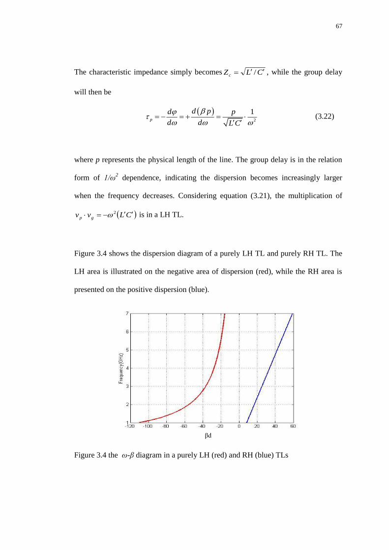
67
The characteristic impedance simply becomes CLZc / , while the group delay
will then be
2
1p
d pd p
d d L C
(3.22)
where p represents the physical length of the line. The group delay is in the relation
form of 1/ω2 dependence, indicating the dispersion becomes increasingly larger
when the frequency decreases. Considering equation (3.21), the multiplication of
CLvv gp 2 is in a LH TL.
Figure 3.4 shows the dispersion diagram of a purely LH TL and purely RH TL. The
LH area is illustrated on the negative area of dispersion (red), while the RH area is
presented on the positive dispersion (blue).
Figure 3.4 the ω-β diagram in a purely LH (red) and RH (blue) TLs
βd
68
In natural, because of unavoidable parasitic series inductance and shunt capacitance,
the dispersion from the PRH contribution is increased with frequency. From
dispersion graph, the backward wave propagation is existed along the LH line as
presenting in negative values (red line). In this range, the line becomes a backward
leaky-wave opposite of the case of conventional RH TL that the dispersion can be
predicted in positive dispersion band (blue line).
3.1.1.2 Equivalent Material Parameters
Both μ(ω) and ε(ω) values in LH material can be derived from the analogy between
the plane wave solution in homogeneous material (Maxwell equations) as well as the
wave along the LH TL (TL equations). In RH TL, the impedance and admittance of
the material are supposed to jZ and jY , respectively, which they have
been changed to CjZ /1 and LjY /1 in the LH TL as shown in
equations (3.23a) and (3.23b)
2
1 10
C C
(3.23a)
2
1 10
L L
(3.23b)
These above equations both demonstrate the negative of μ and ε in a LHM together
with the relative dispersion of the frequency dependence by 1/ω2. Although such a
material does not seem to exist in nature, it might be realized artificially as MTMs
using appropriate implants, as in recent attempts [3.1-3.5]. Only at the occurrence of
frequency dispersion, the simultaneous negative values of ε and μ can be realized. It

69
can be concluded that the LHMs with the dispersive constitutive parameters given by
equations (3.23a) and (3.23b) satisfy the generalized entropy conditions for
dispersive media [3.1], shown in below
0
12
C and
0
12
L (3.24)
Then, the refractive index is derived by taking the square root of the product in
(3.23a) and (3.23b), 0// cjjjYZk rr in plane wave.
For CL /1 , it yields as:
01
2
0
0
CL
c
CLcrr
(3.25)
This last equation confirms the negative value of η(ω) associated with the reversal of
Snell’s law at the interface.
3.1.2 CRLH Theory
In this section, the transmission line approach to CRLH MTMs will be discussed.
The equivalent circuit model of equivalent homogeneous CRLH TL can be shown in
Figure 3.5. For simplicity, only the lossless case of transmission line will be
analyzed. [3.1, 3.17]
70
ΔZ
L’L/ΔZ
C’L/ΔZ
C’RΔZ
L’RΔZ
Figure 3.5 Equivalent circuit model of homogeneous CRLH TL [3.1].
Homogeneous Case
The homogeneous model of a CRLH lossless transmission line shown in Figure 3.5
consists of an inductance L’R in series with a capacitance C'L and a shunt capacitance
C’R in parallel with an inductance L'L. The propagation constant of TL is given
by ''YZj , where Z’ and Y’ are the per-unit length impedance and per-
unit length admittance, respectively. Z’ and Y’ of CRLH TL are defined as
L
R
L
R
LCjY
CLjZ
'
1')('
,'
1')('
(3.26)
Thus, the dispersion relation for a homogenous CRLH TL is
L
R
L
R
LL
RRC
C
L
L
CLCLs
'
'
'
'
''
1'')()(
2
2
(3.27)
Z’
Y’
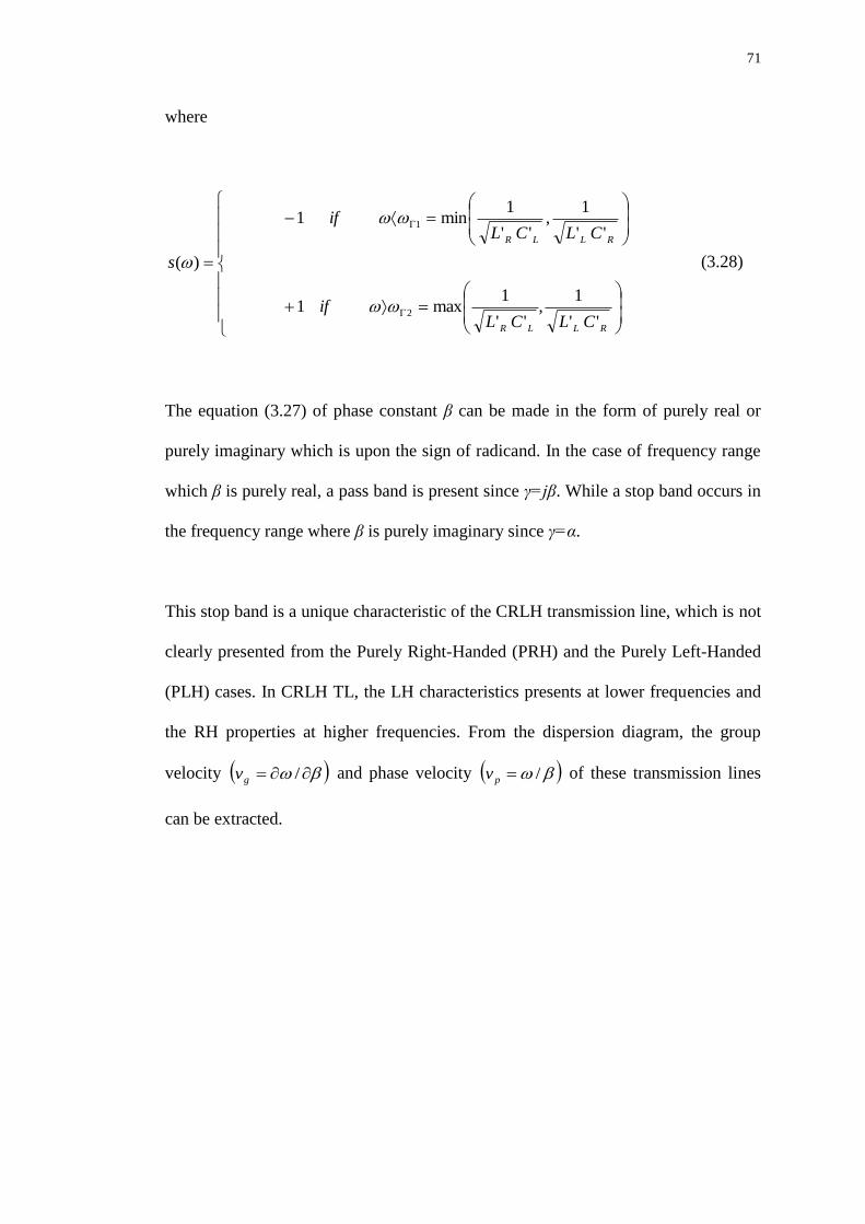
71
where
RLLR
RLLR
CLCLif
CLCLif
s
''
1,
''
1max1
''
1,
''
1min1
)(
2
1
(3.28)
The equation (3.27) of phase constant β can be made in the form of purely real or
purely imaginary which is upon the sign of radicand. In the case of frequency range
which β is purely real, a pass band is present since γ=jβ. While a stop band occurs in
the frequency range where β is purely imaginary since γ=α.
This stop band is a unique characteristic of the CRLH transmission line, which is not
clearly presented from the Purely Right-Handed (PRH) and the Purely Left-Handed
(PLH) cases. In CRLH TL, the LH characteristics presents at lower frequencies and
the RH properties at higher frequencies. From the dispersion diagram, the group
velocity /gv and phase velocity /pv of these transmission lines
can be extracted.
72
Figure 3.6 ω-β or dispersion diagram of a CRLH-TL[3.1].
Considering this diagram, it is found that in a PRH transmission line, vg and vp are
parallel 0pg vv , whereas in PLH transmission line, vg and vp are
antiparallel 0pg vv . In conclusion, the CRLH transmission line has LH
( 0 pg vv ) and RH ( 0 pg vv ) regions. Moreover, Figure 3.6 also illustrates the
stop-band that occurs when γ is purely real for a CRLH transmission line. In the case
of the series and shunt resonances of the CRLH transmission line are equal which is
called the balanced case, which is shown in equation (3.29)
RLLR CLCL (3.29)
This means the LH and RH contribution are exactly balanced, shown in Figure 3.7
The impedance matching is achieved at the frequency where the Bloch impedance
coincides with the reference impedance of the ports; while the phase matching
occurs at those frequencies where the phase shift of the structure is a multiple of π.
β
ωr2
ωr1
ω0
ω

73
2 3 4 5 6 7 8 91 10
-40
-20
-60
0
freq, GHz
dB
(S(2
,1))
7.710G-64.60
m2
Readout
m3
dB
(S(1
,1))
Readout
m4
m2freq=dB(S(2,1))=-64.596
7.710GHz
m3freq=dB(S(2,1))=-81.857
1.310GHzm4freq=dB(S(1,1))=-84.899Valley
3.180GHz
Figure 3.7 Simulated frequency responses of the 30-stage CRLH TL by ADS
simulation, CR=CL=1pF, LR=LL=2.5nH, respectively [3.1].
The ripple occurring in Figure 3.7 is consequence of periodicity and it may limit
filter performance, which means the ripples increase at the edges of the band since
the Bloch impedance takes extreme values. The electrical simulation has been
obtained through ADS. From the example, the 30-cell CRLH TL has the resonate
frequency at f0=3.18GHz. The left handed cut off (fL) is 1.31GHz and the right
handed cut off frequency (fH) is 7.71GHz, respectively
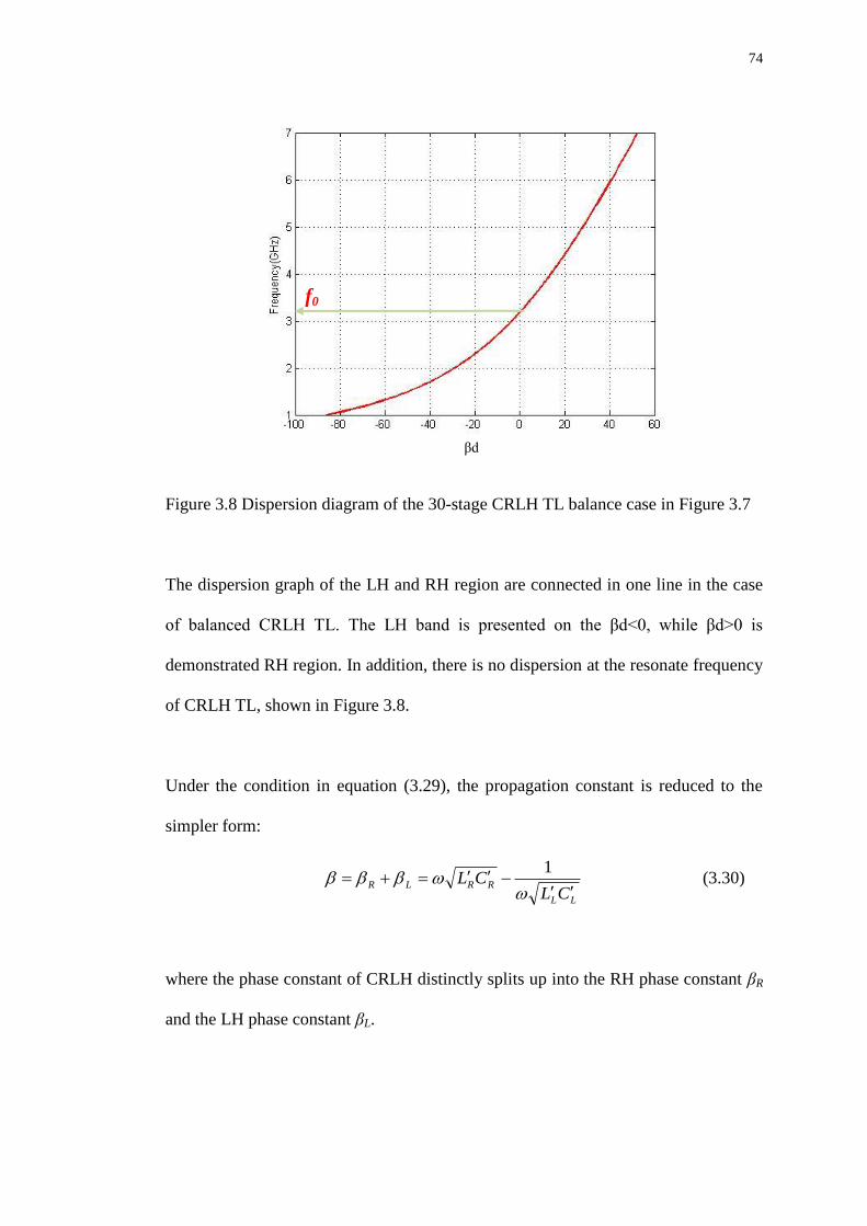
74
Figure 3.8 Dispersion diagram of the 30-stage CRLH TL balance case in Figure 3.7
The dispersion graph of the LH and RH region are connected in one line in the case
of balanced CRLH TL. The LH band is presented on the βd<0, while βd>0 is
demonstrated RH region. In addition, there is no dispersion at the resonate frequency
of CRLH TL, shown in Figure 3.8.
Under the condition in equation (3.29), the propagation constant is reduced to the
simpler form:
LL
RRLRCL
CL
1
(3.30)
where the phase constant of CRLH distinctly splits up into the RH phase constant βR
and the LH phase constant βL.
βd
f0
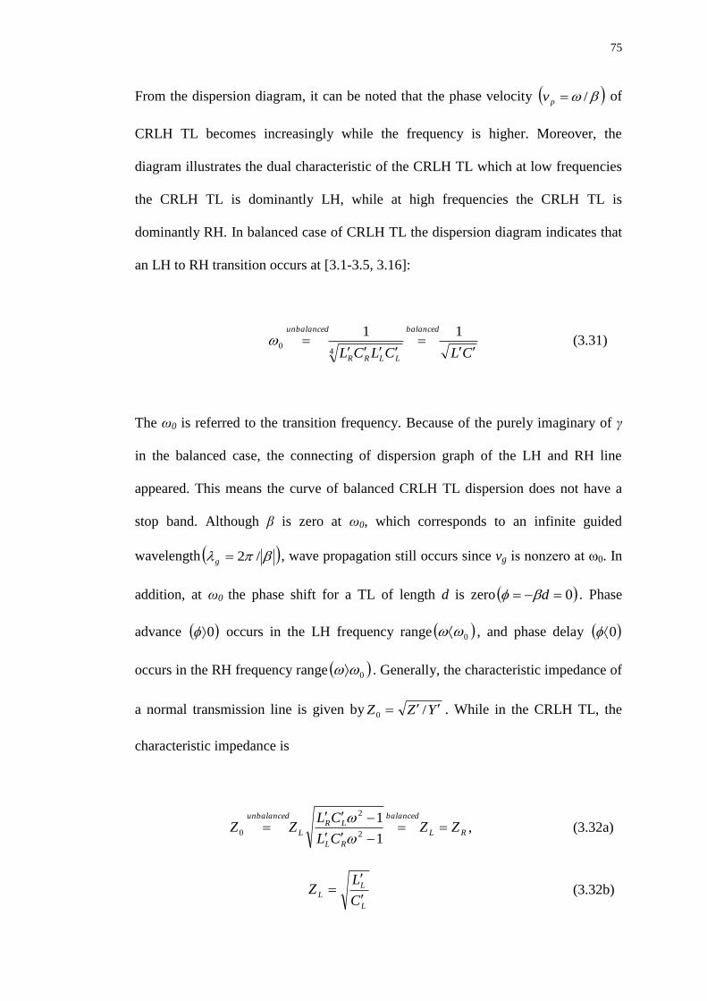
75
From the dispersion diagram, it can be noted that the phase velocity /pv of
CRLH TL becomes increasingly while the frequency is higher. Moreover, the
diagram illustrates the dual characteristic of the CRLH TL which at low frequencies
the CRLH TL is dominantly LH, while at high frequencies the CRLH TL is
dominantly RH. In balanced case of CRLH TL the dispersion diagram indicates that
an LH to RH transition occurs at [3.1-3.5, 3.16]:
CLCLCL
balanced
LLRR
unbalanced
11
40 (3.31)
The ω0 is referred to the transition frequency. Because of the purely imaginary of γ
in the balanced case, the connecting of dispersion graph of the LH and RH line
appeared. This means the curve of balanced CRLH TL dispersion does not have a
stop band. Although β is zero at ω0, which corresponds to an infinite guided
wavelength /2g, wave propagation still occurs since vg is nonzero at ω0. In
addition, at ω0 the phase shift for a TL of length d is zero 0 d . Phase
advance 0 occurs in the LH frequency range 0 , and phase delay 0
occurs in the RH frequency range 0 . Generally, the characteristic impedance of
a normal transmission line is given by YZZ /0. While in the CRLH TL, the
characteristic impedance is
RL
balanced
RL
LRL
unbalanced
ZZCL
CLZZ
1
12
2
0
, (3.32a)
L
LL
C
LZ
(3.32b)
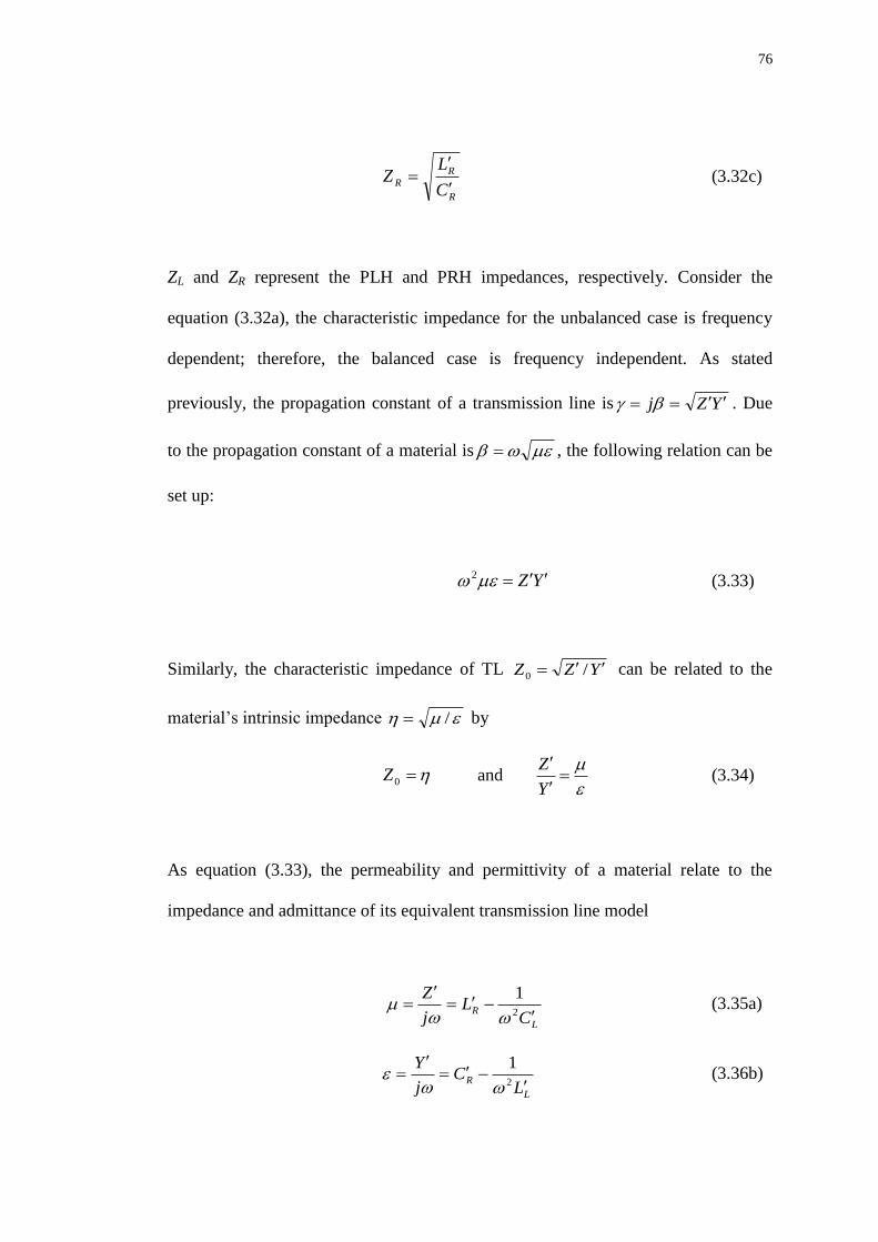
76
R
RR
C
LZ
(3.32c)
ZL and ZR represent the PLH and PRH impedances, respectively. Consider the
equation (3.32a), the characteristic impedance for the unbalanced case is frequency
dependent; therefore, the balanced case is frequency independent. As stated
previously, the propagation constant of a transmission line is YZj . Due
to the propagation constant of a material is , the following relation can be
set up:
YZ 2 (3.33)
Similarly, the characteristic impedance of TL YZZ /0 can be related to the
material’s intrinsic impedance / by
0Z and
Y
Z
(3.34)
As equation (3.33), the permeability and permittivity of a material relate to the
impedance and admittance of its equivalent transmission line model
L
RC
Lj
Z
2
1
(3.35a)
L
RL
Cj
Y
2
1
(3.36b)
77
The refractive index /c for the balanced and unbalanced CRLH TL is
displayed in Figure 3.9.
(a)
(b)
Figure 3.9 (a) Typical index of refraction for the balanced (green) and unbalanced
CRLH TL (red-orange), (b) the refraction index of 30-stage CRLH TL in Figure 3.7
As illustrated in Figure 3.9, a refractive index of the CRLH TL in the LH range is
negative, while it shows the positive values in the RH range (a) [3.1]. In balanced
η
ω
ωr2 ωr1 ω0
f0

78
case CRLH TL, the refractive index is equal to zero on the resonate frequency,
displayed in Figure 3.9(b).
3.2 CSRRs Resonant Type of MTMs TL: Topology, its Equivalent
Circuit and Synthesis
Implementation of resonant type approach can either use CPW or microstrip
transmission line technologies. The CSRRs particles are etched in the ground plane,
underneath the conductor strip so that the CSRRs can be excited by the time varying
electric field of the quasi-TEM signal propagating in the line, while the time varying
magnetic field in CSRRs is applied parallel to the plane of the particle [3.15, 3.18].
The topology of one cell CSRRs can be analyzed by lumped element equivalent T-
circuit model depicted in Figure 3.10 which ignores the losses and inter-resonators
coupling. The model is valid under the condition of small electrical size of CSRRs.
L/2 L/2
LC
C
CC
Cg Cg
(a) (b)
Figure 3.10 Basic cell of CSRRs-based transmission line (a) and equivalent circuit
model, (b) The upper metallization is depicted in black; the slot regions of the
ground plane and depicted in grey [3.19].
ZS ZS
ZP

79
These resonators are extracted to parallel resonant tanks of inductance Lc and
capacitance Cc [3.19-3.24], whereas their coupling to the host line is modeled by the
capacitance C. The series gaps etching above the CSRRs to enhance line-to-CSRRs
coupling are replaced by the capacitance Cg. The series impedance must be
dominated by Cg to achieve the left-handedness condition. In order to simplify the
analysis of the equivalent circuit, the line inductance L is neglected. Normally, L
may not be omitted to describe the accurate structure. These parameters will be used
to model the layout of the CSRRs unit cell to obtain some specific targets.
The study of phase shift of the elemental cell and Bloch impedance; as shown in
equations (3.37) and (3.38), confirms the highly dispersive of the structure:
cos 1
s
p
Z j
Z j
(3.37)
jZjZjZZ pssB 2 (3.38)
where Zs and Zp are the series and shunt impedance of the equivalent T-circuit model
of Figure 3.10, respectively. The ZB and are the key electrical characteristics of
artificial LH lines by CSRRs method, where has to set as the condition of =βl,
β is the phase constant for the Bloch waves, at the operating frequency, while l is the
period of the structure. Therefore, the structure exhibits a band pass behavior with
backward wave propagation in the allowed band from the analysis of equations
(3.37) and (3.38). The flexibility for the artificial lines is dependent on these four
parameters (Zs, Zp, ZB and ).

80
The analysis of the limitation of these circuit parameters are described as follows. In
order to obtain the limit of this LH transmission band, the ZB or have to be forced
to real numbers or positive values and possible for physical implementation
according to:
CC
CL
f
g
cc
L
41
4
1
2
1
(3.39)
cc
HCL
f2
1 (3.40)
fL and fH represent the lower and higher frequency of the interval, respectively. At
these frequencies, both the phase and Bloch impedance take extreme values, for
instance; ZB→∞ and =0 at fH, whereas ZB=0 Ω and =π at fL. In order to wider
the bandwidth, these fL and fH have to be set apart from the cut off frequency (fc) as
much as possible. Analysis of the intrinsic limits of the operative bandwidth is
described as below;
From equations (3.39) and (3.40), the capacitance value of the series gap can be
inferred by
c
c
cc
gZ
C
cos1
cos1
2
1
(3.41)
81
where cc f 2 . Then, the other parameters as follows can be extracted by using
equations (3.37) to (3.40);
22
2222
4cos1
cos1
2Lc
cHLH
H
c
c
cc
c
ZL
(3.42)
2
1
Hc
cL
C
(3.43)
222222
2222
2cos1
cos12
LcHLHcccc
cLcH
ZC
(3.44)
where LL f 2 and HH f 2 . As from equations (3.42) to (3.44), the values of
Cg, Lc, and Cc should be positive to provide the condition of HcL . Since the
angular frequencies which C may be negative, the operative bandwidth is limited by
C which has to force in the real positive number as shown in the condition;
222
222
2cos1LHc
LcH
c
(3.45)
The value of the operating angular frequency, ωc, and phase, øc, only limit the range
of ωL and ωH. At the phase 2/ c , following this rule, by neglecting the L
parameter, the intrinsic limits for ωL and ωH are cLc 2/1 and cH which
might not possible for physical implementation. Thus at the operating frequency, the

82
possibility to control phase and line impedance with a single cell structure will be
analyzed later.
Another interesting point is the transmission zero frequency, fZ, which is extracted
from the simulation or experiment results. At the transmission zero frequency, the
value of phase will be under the condition of 2/ , or 2/2/2/ f , then
after consider the mentioned condition, the latter condition can be demonstrated as;
/ 2 / 22s pZ j Z j (3.46)
Another frequency point, where the second allowed (right handed) band starts up, is
the operating frequency fc. At the operating frequency, the phase variation can be
represented by )( cc f and the image impedance is )( cBc fZZ .These
frequencies are given by the following expressions:
cc
ZCCL
f
2
1 (3.47)
g
cLC
f2
1 (3.48)
In order to extract the parameters at the resonant frequency of the CSRRs, the null
condition of the shunt admittance has been forced, while the impedance from the
input port is set by adding the output impedance (50Ω) and the reactive impedance
of the L and Cg. Using equations (3.40), (3.47), and (3.48), the three elements of the
shunt reactance can be extracted. Because the line inductance, L, cannot be ignored,

83
the Cg must be considered as an effective capacitance by using the simulation of the
equivalent circuit model.
It is noted from all the previous equations that the bandwidth is limited by the
achievable values of C and Cg and it is impossible to simultaneously obtain abrupt
transition bands at the lower and upper edges of the LH band, in addition, the in-
band ripple is expected as consequence of periodicity. While the transmission zero
frequency is forced to be nearer the lower edge of the band, the gap capacitance Cg
have to make highly as comparing to the coupling capacitance C. As a result, the
appearance of a highly selective filter is provided at the lower band edge. As refer to
equations (3.39) and (3.40), it appears that the bandwidth is dependent on the values
of Cg and C, and it is difficult to design wide (or even moderate) band structures
[3.22].
3.3 Electric, Magnetic Coupling and the new Equivalent Circuit
Model
All previously published works of CSRRs have assumed that the coupling between
the rings in adjacent cells is dominated by the electric coupling and magnetic
coupling can be neglected [3.19-3.24]. However, it is revealed that there are strong
magnetic couplings between the adjacent rings, resulting in significant effects on
circuit performance. This section presents a new equivalent circuit model. The model
has been developed and verified both numerically and experimentally to take into
account of the magnetic coupling between the rings in adjacent cells, which has been
neglected so far.

84
To observe this effect, a simple 2-cell CSRRs microstrip TL, shown in Figure 3.11
was designed and analyzed, aiming to understand the coupling effects between the
CSRRs.
(a)
(b)
Figure 3.11 (a) The topology of CSRRs unit cell and (b) 2-cells CSRRs microstrip
TL and its magnetic field distribution at 2.4GHz
The example in Figure 3.11 demonstrates the qualification of the 2-cell CSRRs when
added the series gaps on the strip line. As shown in this figure, the narrow pass band
is occurred and this also generates the left hand wave. The Rogers RO3010 substrate
has been chosen (thickness h=1.27mm, εr=10.2) for this electromagnetic simulation.
Rext
C
d
Cell separation=0.2mm

85
In the design the transmission line strip width is of 3.2mm, the thickness of substrate
1.27mm, the external radius of the ring (Rext) 3.5mm, the metal ring width (c)
0.4mm, and the gap between the inner and outer rings (d) 0.3mm. The total length of
the 2-cell CSRRs line is 15mm. Separation between the two cells is initially set to
0.2mm and finally reaches to 1mm by increasing 0.2mm at each step.
Electric_field
0
5000
10000
15000
20000
25000
30000
0.2 0.4 0.6 0.8 1
distance (mm)
Vol
ts p
er M
etre
(a)
Magnetic-field
0
50
100
150
200
250
0.2 0.4 0.6 0.8 1
distance (mm)
Am
pere
s pe
r M
etre
(b)
Figure 3.12 Field variations with ring separation of the two CSRRs (a) Electric field
and (b) Magnetic field at 2.4GHz
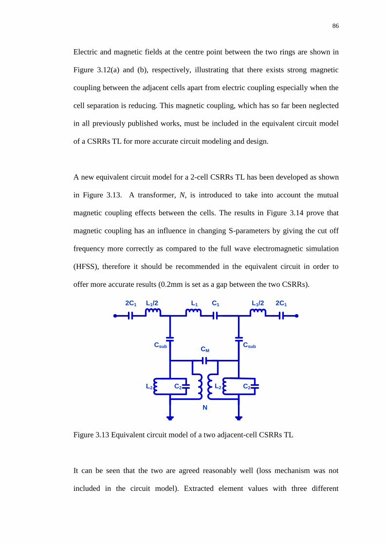
86
Electric and magnetic fields at the centre point between the two rings are shown in
Figure 3.12(a) and (b), respectively, illustrating that there exists strong magnetic
coupling between the adjacent cells apart from electric coupling especially when the
cell separation is reducing. This magnetic coupling, which has so far been neglected
in all previously published works, must be included in the equivalent circuit model
of a CSRRs TL for more accurate circuit modeling and design.
A new equivalent circuit model for a 2-cell CSRRs TL has been developed as shown
in Figure 3.13. A transformer, N, is introduced to take into account the mutual
magnetic coupling effects between the cells. The results in Figure 3.14 prove that
magnetic coupling has an influence in changing S-parameters by giving the cut off
frequency more correctly as compared to the full wave electromagnetic simulation
(HFSS), therefore it should be recommended in the equivalent circuit in order to
offer more accurate results (0.2mm is set as a gap between the two CSRRs).
L1/2 L1
L2
2C1 C1
CsubCM
C2
L1/2
L2
2C1
Csub
C2
N
Figure 3.13 Equivalent circuit model of a two adjacent-cell CSRRs TL
It can be seen that the two are agreed reasonably well (loss mechanism was not
included in the circuit model). Extracted element values with three different
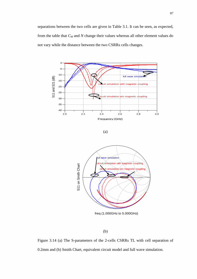
87
separations between the two cells are given in Table 3.1. It can be seen, as expected,
from the table that CM and N change their values whereas all other element values do
not vary while the distance between the two CSRRs cells changes.
2.2 2.4 2.6 2.82.0 3.0
-35
-30
-25
-20
-15
-10
-5
-40
0
Frequency (GHz)
S11
and
S21
(dB
) full wave simulation
circuit simulation w/o magnetic coupling
circuit simulation with magnetic coupling
(a)
freq (1.000GHz to 5.000GHz)
S11 o
n S
mith
Chart
circuit simulation w/o magnetic coupling
circuit simulation with magnetic coupling
full wave simulation
(b)
Figure 3.14 (a) The S-parameters of the 2-cells CSRRs TL with cell separation of
0.2mm and (b) Smith Chart, equivalent circuit model and full wave simulation.

88
It has been found that the magnetic coupling which takes into account in the case of
the two adjacent CSRR cell can provide the S11 graph obviously closer to the S11
from HFSS full wave simulation at 2.27GHz. If considering the circuit simulation
without taking into account of the magnetic coupling, the S11 graph (dash line)
displays the centre frequency at 2.3GHz which is not exposed the precise centre
frequency. On Smith Chart, the S11 of the new equivalent circuit provides a better
match of the graph especially on the passband than the equivalent circuit without
magnetic coupling. The rational of transformer proves that there is strong magnetic
coupling between the rings when they are closely placed.
Table 3.1 Extracted Element Parameters for the 2-cell CSRRs TL
Distance between Cell
(mm) C1(pF) C2(pF) L1(nH) L2(nH) CM(pF) N(turns)
0.1 1.3573 2.5075 0.8092 1.57 5.4 1.36
0.5 1.3573 2.5075 0.8092 1.57 4 1.12
1 1.3573 2.5075 0.8092 1.57 0.6 1.09
3.4 Analyzing the LH operating area of CSRRs TL
As mention at the beginning of this chapter, a CSRRs applied with series gap on host
line exhibits LH properties. In order to verify the Left handed characteristics, the LH
region of CSRRs TL has to be designated. In this section, a 4-unit cell CSRRs
transmission line, shown in Figure 3.15, was represented for consideration. The 4-

89
cell CSRRs TL has been fabricated on the Rogers RO3010 substrate, with a
thickness h of 1.27mm, dielectric constant εr =10.2, rext=3.4mm, c=0.4mm,
d=0.3mm. The width of the TL was designed to achieve 50Ω characteristic
impedance at the operating frequency.
Based on the analysis in magnetic coupling, the geometry of a 4-cells CSRRs TL
placed by cells 1-2 is 1mm, cells 2-3 2mm, cells 3-4 1mm, as shown in Figure 3.15
(a).
(a)
(b)
Figure 3.15 The prototype of 4-cell CSRRs TL, (a) backside view and (b) top view.
N N
4 3 2 1

90
CSRRs TLs has a total physical length of 35 mm and were fabricated The S-
parameters were measured using Agilent E8364A Network Analyzer, shown in
Figure 3.16. The lower passband and higher passband of the CSRRs TL are
measured to be 2.2 and 2.5GHz respectively, displayed as narrow passband on
Figure 3.16(a), the centre of operating area gives highest transmitted signal with
lower loss; however there are some substrate and metal losses. The insertion loss at
this point is approximately 2.49dB. In addition, the phase compression has appeared
within the LH passband (2-3GHz) of the CSRRs TL, shown on Figure 3.16(b).
2 3 4 5 61 7
-50
-40
-30
-20
-10
-60
0
Frequency (GHz)
S11
and
S21
(dB)
S21
S11
(a)
2 3 4 5 61 7
-100
0
100
-200
200
Frequency (GHz)
Phas
e S21
(deg
rees
)
(b)
Figure 3.16 The measured results of (a) S-parameters of 4 CSRRs cells and (b) Phase
of S21.

91
The circuit model as shown in Figure 3.13 is used here again to extract the loading
parameters (C1, Csub, C2, L2, and L1). These parameters were used to model a cell of
CSRRs before cascading them as 4 cells to fit with the measurement. By fitting the
curve with the measurement results, the extracted parameters can be found as
(C1=1.1787pF, Csub=1.4476pF, C2=3.007pF; L2=1.276nH, L1=1.009nH, N=1.08 and
CM=0.59pF), seen in Figure 3.17. The S parameters (S21 and S11) of both
measurement and simulation agree well. The passband has been correctly predicted.
Measurement
Circuit simulation
2 3 4 5 61 7
-40
-20
-60
0
Frequency (GHz)
S1
1 a
nd
S2
1 (
dB
)
Figure 3.17 The S-parameters (S21 and S11) by circuit simulation and measurement
The discrepancies between the simulated and measured data in the stop band are
probably due to the fabrication tolerance in our PCB laboratory, especially the
alignment between the metal strip on the top of the substrate and the CSRRs on
ground plane. However, the new equivalent circuit model that takes into account of
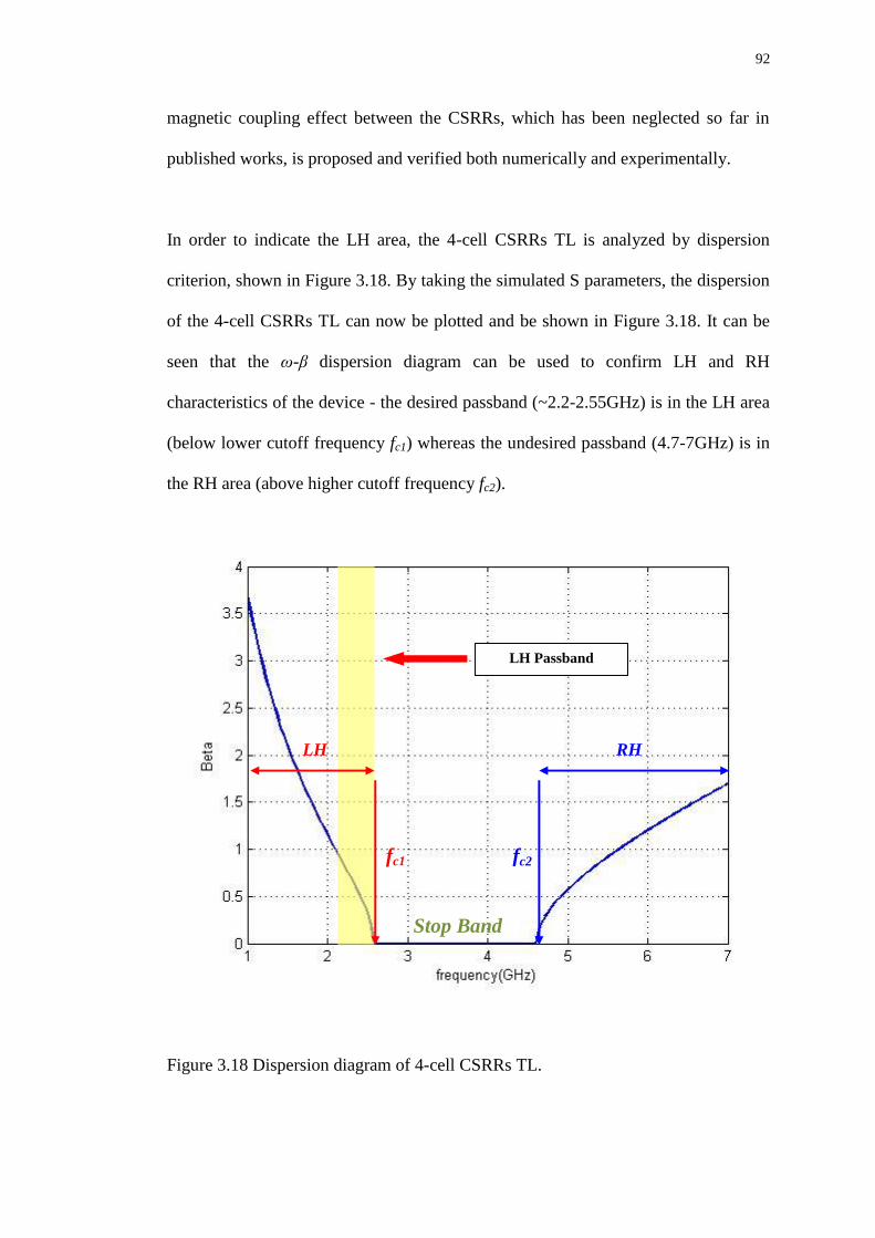
92
magnetic coupling effect between the CSRRs, which has been neglected so far in
published works, is proposed and verified both numerically and experimentally.
In order to indicate the LH area, the 4-cell CSRRs TL is analyzed by dispersion
criterion, shown in Figure 3.18. By taking the simulated S parameters, the dispersion
of the 4-cell CSRRs TL can now be plotted and be shown in Figure 3.18. It can be
seen that the ω-β dispersion diagram can be used to confirm LH and RH
characteristics of the device - the desired passband (~2.2-2.55GHz) is in the LH area
(below lower cutoff frequency fc1) whereas the undesired passband (4.7-7GHz) is in
the RH area (above higher cutoff frequency fc2).
Figure 3.18 Dispersion diagram of 4-cell CSRRs TL.
Stop Band
LH Passband
fc1
LH RH
fc2

93
The dispersion graph exhibits a very different behavior of the CSRRs TL especially
in the LH passband that provides higher dispersion slope comparing to the RH area.
This means when the input wave gets close to the left hand side of the lower cutoff
(fc1), the observed wave is obviously transformed the shape of the original wave
since the high dispersion which cannot be predicted as in the ideal TL case. This
behavior is explained by the fact that the backward wave effect of the periodic
(artificial) MTM transmission line which becomes dominant over the ideal TL. At
the dispersion effect higher than fc1; the dispersion ω-β curve exhibits a zero slope
there, corresponding to vg=0, until reaching the RH area.

94
3.5 Conclusion
In this chapter, we have derived the three-type TL; the purely LH TL, the CRLH TL,
and the CSRRs TL. The dispersion properties versus frequency of them have been
analyzed, including their phase and group velocities. In LH area, the sign of phase
and group velocities in LH TL are opposite, unlikely in RH area owing to the
backward wave propagation. Moreover, it is found that both CRLH and CSRRs TL
provide LH and RH area. In balanced CRLH TL case, the LH and RH area can be
merged to exhibit broader passband. Although the equivalent circuit of CSRRs TL
has been analyzed in many years, the magnetic coupling is still not taken into
account to the equivalent circuit. This chapter also recommends the new equivalent
circuit model of the CSRRs TL under the two more unit cell adjacent. The simulated
scattering parameters are presented in the case of with and without the magnetic
coupling. The results show that the magnetic coupling should be added in the
equivalent circuit model as a good agreement of both simulation and measurement
results as well as the indicating of LH and RH area.
95
3.6 References
[3.1] C. Caloz and T. Itoh, ELECTROMAGNETIC METAMATERIALS:
TRANSMISSION LINE THEORY AND MICROWAVE APPLICATIONS, John
Wiley &Sons, Inc., 2006
[3.2] G. V. Eleftheriades, A. K. Iyer, and P. C. Kremer, “Planar refractive index
media using periodically L-C loaded transmission lines”, IEEE Trans.
Microwave Theory Tech., vol. 50, pp. 2702-2712, Dec 2002
[3.3] C. Caloz and T. Itoh, “Novel microwave devices and structures based on the
transmission line approach of meta-materials”, IEEE-MTT Int’ l Symp., vol.
1, pp. 195-198, Philadelphia, PA, June 2003
[3.4] C. Caloz and T. Itoh, ”Transmission Line Approach of Left-Handed (LH)
Materials and Microstrip Implementation of an Artificial LH Transmission
Line”, IEEE Trans. Antenna and propagation, vol. 52, no.5, pp. 1159-1166,
May 2004
[3.5] A. Lai and T. Itoh, “Composite Right/Left-handed Transmission Line
Metamaterials”, IEEE Microwave magazine, pp. 35-48, Sept 2004
[3.6] J. -Q. Gong and Q. -X. Chu, “Synthesis of Resonant-Type CRLH
Transmission Lines Based on CSRR with Dual Band Behavior”,
ICMMT2008 Proceeding, 2008
[3.7] J. Bonache, M. Gil, I. Gil, J. G. Garcia, and F. Martin, “Limitations and
Solutions of Resonant-Type Metamaterial Transmission Lines for Filter
Applications: the Hybrid Approach”, Microwave Symposium Digest, 2006,
IEEE MTT-S International, US, pp. 939-942, 2006

96
[3.8] W. Wei and H. Li, “Inhomogeneous Composite Right’/Left-Handed
Transmission Line”, ICMMT2008 Proceeding, 978-1-4244-1880-0/08
[3.9] A. F. Abdelaziz, T. M. Abuelfadl, and O. L. Elsayed, “Realization of
composite right/left-handed transmission line using coupled lines”, Progress
In Electromagnetics Research, PIER 92, pp. 299-315, 2009
[3.10] C. Caloz, S. Abielmona, H. V. Nguyen, and A. Rennings, “Dual composite
right/left-handed (D-CRLH) leaky-wave antenna with low beam squinting
and tunable group velocity”, Phys. Stat. sol., no. 4, pp. 1219-1226, Mar 2007
[3.11] S. N. Burokur, M. Latrach, and S. Toutain, “Study of the effect of dielectric
split-ring resonators on microstrip line transmission”, Microwave Opt Techno
Lett, vol. 44, pp. 445-8, Mar 2005
[3.12] M. Kafesaki, T. Koschny, and R. Penciu, “Left-handed metamaterials:
detailed numerical studies of the transmission properties”, J. Optics A: Pure
Applied Optics 7, pp. S12-S22, 2005
[3.13] I. Gil, J. Bonache, M. Gil, J. G. Garcia, and F. Martin, “Accurate circuit
analysis of resonant-type left handed transmission lines with inter-resonator
coupling” Journal of applied physics, vol. 100, Oct 2006
[3.14] I. Gil, J. Bonache, M. Gil, J. G. Garcia, F. Martin, and R. Marques,
“Modeling complementary split rings resonator (CSRR) left-handed lines
with inter-resonator’s coupling”, IEEE Melecon 2006, pp. 225-228, May
2006
[3.15] K. Aydin, K. Guven, M. Kafesaki, L. Zhang, C. M. Soukoulis, and E. Ozbay,
“Experimental observation of true left-handed transmission peaks in
metamaterials”, Optics Letters, vol. 29, no. 22, pp. 2623-2625, Nov 2004
97
[3.16] C. Caloz and T. Itoh, “Transmission Line Approach of Left-Handed (LH)
Materials and Microstrip Implementation of an Artificial LH Transmission
Line”, IEEE Transaction on Antennas and Propagation, vol. 52, no. 5, pp.
1159-1166, May 2004
[3.17] D. M. Pozar, MICROWAVE ENGINEERING 3rd
edition, J. Wiley &Sons,
2005
[3.18] M. Beruete, M. Aznabet & etc., “Electroinductive waves role in left-handed
stacked complementary split rings resonators”, Optics Express, vol. 17, no. 3,
pp. 1274-1281, Feb 2009
[3.19] M. Gil, J. Bonache, I. Gil, J. G. Garcia, and F. Martin, “On the transmission
properties of left-handed microstrip lines implemented by complementary
split rings resonators”, Int. J. Numer. Model, pp. 87-103, John Wiley &Sons,
Ltd., 2006
[3.20] J. Bonache, F. Martin, I. Gil, J. G. Garcia, R. Marques, and M. Sorolla,
“Microstrip Bandpass Filters with Wide Bandwidth and Compact
Dimensions”, Microwave and Optical Technology Letters, Vol.45, No.4, Aug
2005, pp. 343-346.
[3.21] I. Gil, J. Bonache, M. Gil, J. G. Garcia, and F. Martin, “Left-handed and
Right-handed transmission properties of microstrip lines loaded with
complementary split rings resonators”, Microwave and Optical Technology
Letters, Vol.48, No.12, Dec 2006, pp. 2508-2511
[3.22] I. Gil, J. Bonache, M. Gil, J. G. Garcia, and F. Martin, “Accurate circuit
analysis of resonant-type left-handed transmission lines with inter-resonator
coupling”, Journal of Applied Phy., 100, 2006, pp. 07498-1-10.

98
[3.23] J. Bonache, M. Gil, I. Gil, J. G. Garcia, and F. Martin, “Limitations and
Solutions of Resonant-Type Metamaterial Transmission Lines for Filter
Applications: the Hybrid Approach”, IEEE Microwave Symposium Digest,
2006, pp. 939-942
[3.24] G. Siso, M. Gil, J. Bonache, and F. Martin, “On the dispersion characteristics
of metamaterials transmission lines”, Journal of applied physics, vol. 102,
Oct 2007

99
CHAPTER 4
METAMATERIAL DELAY LINE USING COMPLEMENTARY
SPLIT RING RESONATORS
INTRODUCTION
Digital communications have become more and more important in our life; as a
result highly complex data processing is required. Group delay seems to be a main
problem that degrades system performance for frequency selective components.
There have been many works in analyzing and suppressing group delay on signal
distortion [4.1-4.8] such as a loaded transmission line with a varactor diode [4.5], a
surface acoustic wave (SAW) [4.6], and a magneto-static wave (MSW) [4.7, 4.8]. In
communication systems, there are many sources, especially co-channel interference,
leading to interference between communication channels. Recently, a controlled
signal delay has been used in signal processing instead of simply suppressing the
group delay [4.9-4.14].
However, the characteristic of metamaterial CSRRs lines as dispersive transmission
lines in group delay has not been well developed. Due to its compactness and unique
electrical properties, the prototype of the 4-cell CSRRs TL has been investigated as a
passive delay line. The simulated and measured group delay and signal delay results
are well established with the dispersion relation of CSRRs TL. Also, a significantly
larger group delay of the CSRRs TL than the conventional TL is presented.
Furthermore, the active tunable delay line has been studied by embedding the 4-cell
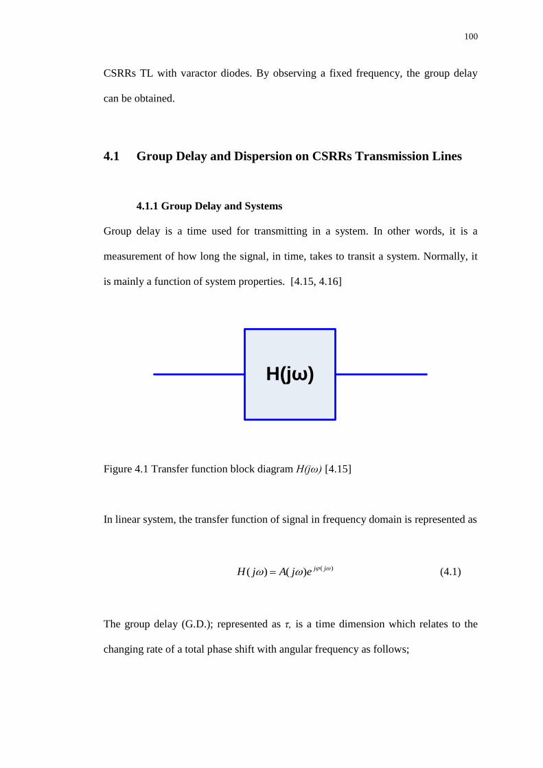
100
CSRRs TL with varactor diodes. By observing a fixed frequency, the group delay
can be obtained.
4.1 Group Delay and Dispersion on CSRRs Transmission Lines
4.1.1 Group Delay and Systems
Group delay is a time used for transmitting in a system. In other words, it is a
measurement of how long the signal, in time, takes to transit a system. Normally, it
is mainly a function of system properties. [4.15, 4.16]
H(jω)
Figure 4.1 Transfer function block diagram H(jω) [4.15]
In linear system, the transfer function of signal in frequency domain is represented as
)()()( jjejAjH (4.1)
The group delay (G.D.); represented as τ, is a time dimension which relates to the
changing rate of a total phase shift with angular frequency as follows;
101
)()(..
DG
(4.2)
where φ and ω are the total phase shift and the angular frequency, respectively.
Group delay; sometimes called “envelope delay”, also can be expressed as the form
of a differential equation of phase variation at the operating frequency. Group delay
can be described as the time delay of the amplitude envelope of a narrow group at
the frequencies around specific frequency.
As shown in equation (4.2), the group delay is negatively proportional to frequency.
The delay signal (τ) represents as a function of
jejH )( (4.3)
Which shows that the envelope of the signal delay is a form of group delay.
4.1.2 The dispersion properties and group delay of a CSRRs TL
Dispersion is the phenomenon where the original wave change of waveform after
propagating through a medium which is dependent upon that wave’s frequency. This
phenomenon also provides a difference in phase velocities due to different
frequencies. However, in some specific materials, the dispersion can be controlled
and functionalized with various phase manipulation effects [4.17-4.19].

102
In order to compare the group delay of CSRRs TL, the fundamental mode of
dispersion with relation to MTMs TL can be analyzed as [4.20];
CSRR RH LH L
R
(4.4)
, with 1/R R RL C and 1/L L LL C
where ωR and ωL are the cut off frequency of right-handed and left-handed
passbands.
The first term is represented as the conventional part of the line, while the last term
is the effect by left-handed wave propagation. Therefore, in a LH passband, the
phase velocity (vp) and the corresponding group velocity (vg) are
2
p
L
v
(4.5)
2
1
/c
cg c
L
v d d
Then, the group delay in a CSRRs TL on a LH area can be given as [4.20, 4.21];
2( )
N Lg c
c
ddN
d d
(4.6)
Where ϕ is the transmission phase, ωc is the observed frequency on the LH passband
and N is the number of CSRRs cells.

103
In the case of a conventional TL, the group delay is given only by the RH effect
which can be presented as;
1
g
R
l
(4.7)
where l is the length of transmission line.
As shown in equation (4.6) and (4.7), the group delay of any signals travelled
through a CSRRs TL can be varied in the LH area which is dependent on the input
signal frequency (ωc) and a number of CSRRs cells (N). Whereas, the delay time of
different signal frequencies through a conventional TL is constant. Hence at a LH
certain frequency band, a CSRRs TL can provide different time delay by frequency
function. Therefore, by fixing the parameter N with 4-cell CSRRs in this chapter, a
signal delay at the another end of the CSRRs TL are observed.
4.2 Passive CSRRs Model and Delay Line Design Procedures
Due to unique dispersion characteristics of MTM TLs, as compared to conventional
TLs, the group delay and their signal delays of the 4-cell CSRRs microstrip TLs are
analyzed by both simulation and measurement. Since the CSRRs loaded
transmission line is fixed, both applied models are called “Passive model delay line”.

104
(a)
(b) (c)
Figure 4.2 (a) The topology of a unit cell CSRRs TL and Photographs of the
designed 4 –cell CSRRs TL ;(b) ground view, (c) microstrip top view
Figure 4.2 illustrates the dimensions of designed 4-cell CSRRs delay line which is
implemented on the Roger (RO3010) substrate with εr = 10.2 and 1.27mm thickness,
In the design the transmission line strip width is adjusted to obtain 50Ω matching
network, the external radius of the ring (Rext) 3.4mm, the metal ring width (c)
0.4mm, and the gap between the inner and outer rings (d) 0.3mm. The total length of
the 4-cells CSRRs TL is 35mm. The equivalent circuit model of this optimized 4-cell
CSRRs delay line is shown in the previous chapter. The S-parameter measurement is
carried out using Network Analyzer (Agilent E8364A).
C d
Rext
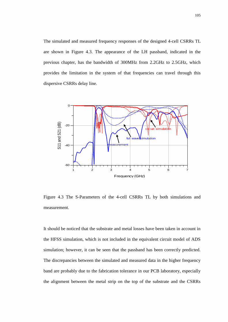
105
The simulated and measured frequency responses of the designed 4-cell CSRRs TL
are shown in Figure 4.3. The appearance of the LH passband, indicated in the
previous chapter, has the bandwidth of 300MHz from 2.2GHz to 2.5GHz, which
provides the limitation in the system of that frequencies can travel through this
dispersive CSRRs delay line.
measurement
full wave simulation
circuit simulation
2 3 4 5 61 7
-40
-20
-60
0
Frequency (GHz)
S11
and
S21
(dB
)
Figure 4.3 The S-Parameters of the 4-cell CSRRs TL by both simulations and
measurement.
It should be noticed that the substrate and metal losses have been taken in account in
the HFSS simulation, which is not included in the equivalent circuit model of ADS
simulation; however, it can be seen that the passband has been correctly predicted.
The discrepancies between the simulated and measured data in the higher frequency
band are probably due to the fabrication tolerance in our PCB laboratory, especially
the alignment between the metal strip on the top of the substrate and the CSRRs
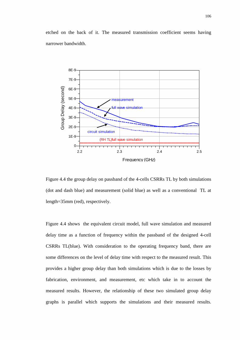
106
etched on the back of it. The measured transmission coefficient seems having
narrower bandwidth.
2.3 2.42.2 2.5
1E-9
2E-9
3E-9
4E-9
5E-9
6E-9
7E-9
0
8E-9
Frequency (GHz)
Gro
up
De
lay (
se
co
nd
)
measurement
full wave simulation
circuit simulation
(RH TL)full wave simulation
Figure 4.4 the group delay on passband of the 4-cells CSRRs TL by both simulations
(dot and dash blue) and measurement (solid blue) as well as a conventional TL at
length=35mm (red), respectively.
Figure 4.4 shows the equivalent circuit model, full wave simulation and measured
delay time as a function of frequency within the passband of the designed 4-cell
CSRRs TL(blue). With consideration to the operating frequency band, there are
some differences on the level of delay time with respect to the measured result. This
provides a higher group delay than both simulations which is due to the losses by
fabrication, environment, and measurement, etc which take in to account the
measured results. However, the relationship of these two simulated group delay
graphs is parallel which supports the simulations and their measured results.

107
Especially, the HFSS full wave simulation results (dash blue), the group delay graph
seems to get closer to the measured group delay result (solid blue).
In both simulated and measured results, the slope of group delay obviously rises at
the frequency near the lower cutoff frequency which is 2.2GHz at 4.6ns, (by
measurement) 2.3GHz at 3ns and 2.4GHz at 2ns, respectively. At 2.4 and 2.5GHz,
the delay can be assumed to be stable at 2ns which supports the analyzed group
delay relation happening in LH area of the delay line that it is inversely proportional
with respect to frequency.
For comparison purpose, the full wave simulated group delay of the conventional TL
with the same length (35mm) is represented as RH TL in Figure 4.4 (solid red). Its
group delay tends to be stable at 0.3ns all frequencies which presents as 10 times of
the CSRRs TL when observing at the mid passband 2.3GHz. These significantly
group delay results are very useful for size and cost reduction in communication
system especially in radar applications.
Delay lines can be very useful in signal processing such as for some radar or
telecommunication applications. It is necessary to multiplex the multiple signals at
the transmitter in the form of a single, complex signal and de-multiplex each
individual signal at the receiver end. The diagram of a simple RF system is shown in
Figure 4.5.
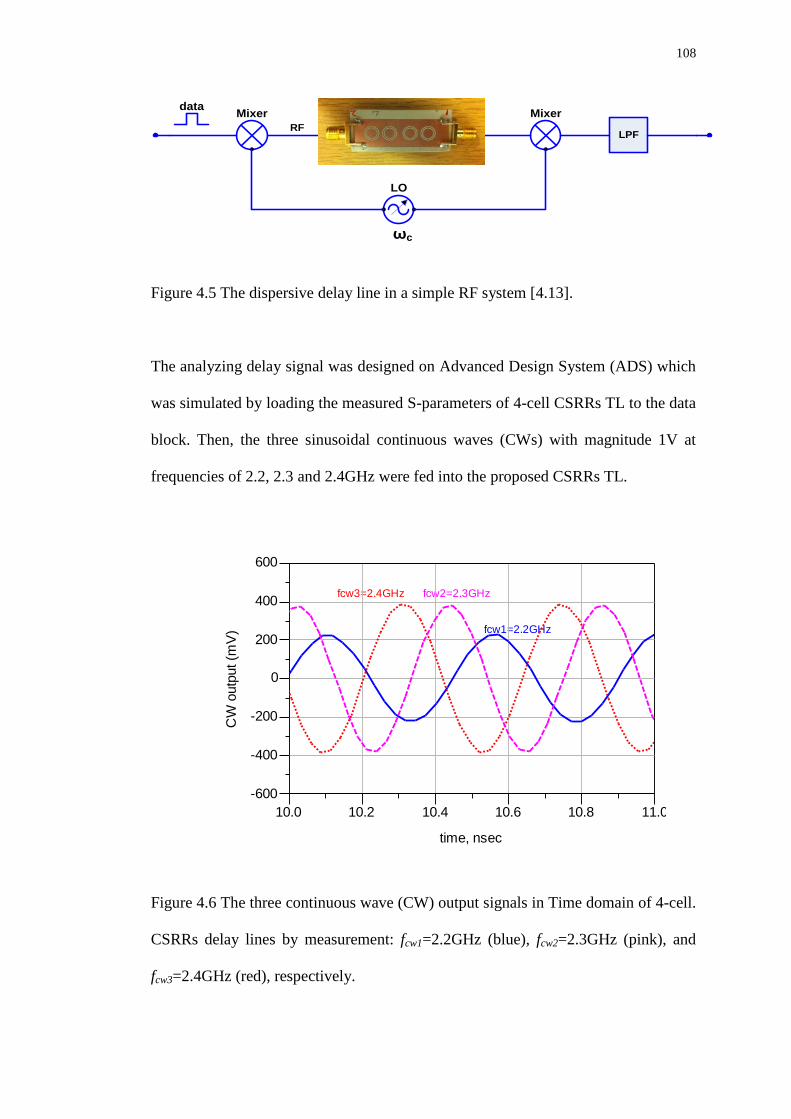
108
ωc
data
CSRRs TL
Mixer Mixer
RF
LO
LPF
Figure 4.5 The dispersive delay line in a simple RF system [4.13].
The analyzing delay signal was designed on Advanced Design System (ADS) which
was simulated by loading the measured S-parameters of 4-cell CSRRs TL to the data
block. Then, the three sinusoidal continuous waves (CWs) with magnitude 1V at
frequencies of 2.2, 2.3 and 2.4GHz were fed into the proposed CSRRs TL.
fcw1=2.2GHz
fcw2=2.3GHzfcw3=2.4GHz
10.2 10.4 10.6 10.810.0 11.0
-400
-200
0
200
400
-600
600
time, nsec
CW
outp
ut (m
V)
Figure 4.6 The three continuous wave (CW) output signals in Time domain of 4-cell.
CSRRs delay lines by measurement: fcw1=2.2GHz (blue), fcw2=2.3GHz (pink), and
fcw3=2.4GHz (red), respectively.

109
At the output end, the different signals in phase and times are extracted and shown in
Figure 4.6. Because the CSRRs TL acts as a narrow bandpass filter, the delay of a
continuous wave cannot obviously be indicated. However, the signal properties and
delays can be analyzed by observing the steady state of the signals.
Due to the relation between dispersion and group delay, the three sinusoidal waves
can clearly be seen both time differences of their amplitudes and phases at the output
port. The CW frequencies that are nearer the higher cutoff frequency (2.3 and
2.4GHz), presents less suffering from dispersion and consume less delay than the
CW frequency (2.2GHz) which is near the lower cutoff frequency.
In order to present the clear view of group delay in CSRRs TL, the pulse signals,
which are represented as digital data in communication systems, are fed in the
system in Figure 4.5. It is shown that the modulated pulse with carrier fc2=2.5GHz
(solid blue) is delayed less as it transmits with the peak propagated time at 5ns,
whereas the modulated pulse with the lower carrier fc1=2.25GHz (dot red) has a
time delay at 6ns which displays the peak voltage, illustrated in Figure 4.7.

110
5 10 15 20 250 30
-150
-100
-50
0
50
100
150
-200
200
time, nsec
Outp
ut dela
y s
ignal1
and 2
(m
V)
Figure 4.7 the modulated output signals with different carriers ( fc1=2.25GHz in dot
red and fc2=2.5GHz in solid blue).
In order to make a clear view of the signal delay and group delay, the envelope
detection of the two input pulses have been considered in the magnitude voltage and
time relation, illustrated in Figure 4.8.
It is obvious that the pulse signal of carrier frequency at 2.25GHz (dash pink)
consumes the time via the 4-cell CSRRs TL more than the pulse signal of the carrier
frequency at 2.5GHz (red) by 1ns delay difference and 3.5ns from the midpoint of
the original pulse. These time differences between the input and output pulses are
matched with the group delay graph in Figure 4.4.
fc2=2.5GHz fc1=2.25GHz

111
5 10 15 20 250 30
0.1
0.2
0.3
0.4
0.5
0.0
0.6
0.05
0.10
0.15
0.00
0.20
time, nsec
Ou
tpu
t Sig
na
l1 a
nd
2 (V
)
Inp
ut
pu
lse
(V
)
Figure 4.8 The Envelopes of RF Pulse fc1 and fc2 in time domain compared to input
after travelling through the 4-cell CSRRs by the measured S-parameters
Therefore, the signals at the output of the delay line can be functioned and extracted
in both CW and Pulse signals. It can be seen clearly that the signals sent through the
CSRRs TL provide different delays for different frequency signals and a much
longer delay with much compact size in comparison with a conventional TL, the
more complex data can be sent at the same time without increasing the system
complexity.
fc2=2.5GHz
fc1=2.25GHz
Input pulse

112
4.3 Active CSRRs Model and Delay Line
There are many reviews that present a varactor diode for a tuning part in
transmission lines. Especially in the recent years, the applied diodes for a large group
delay have been reviewed [4.23, 4.24]. Besides the passive tunable CSRRs delay
line, that is presented previously, the active tunable CSRRs delay line, by embedding
varactor diodes into the 4-cell CSRRs TL is now performed. Because the varactor
diode can act as a small inherence capacitor after changing the applied voltage, the
four varactor diodes (BB833 Infineon Technologies) are placed in the 4-cell CSRRs
TL as demonstrated in Figure 4.9(a). Lchoke, representing a thin wire linked between
the varactor diode and the strip, Rvar and Cvar representing the varactor loss and
junction capacitor, respectively.
The fabricated active tunable CSRRs TL for 4-cascaded cells is depicted in Figure
4.9(b) and (c) by following the dimensions of the 4-cell CSRRs TL. The
measurement is carried out using Agilent E8364A Vector Network Analyzer. The
DC bias voltages vary from 0V to -20V.
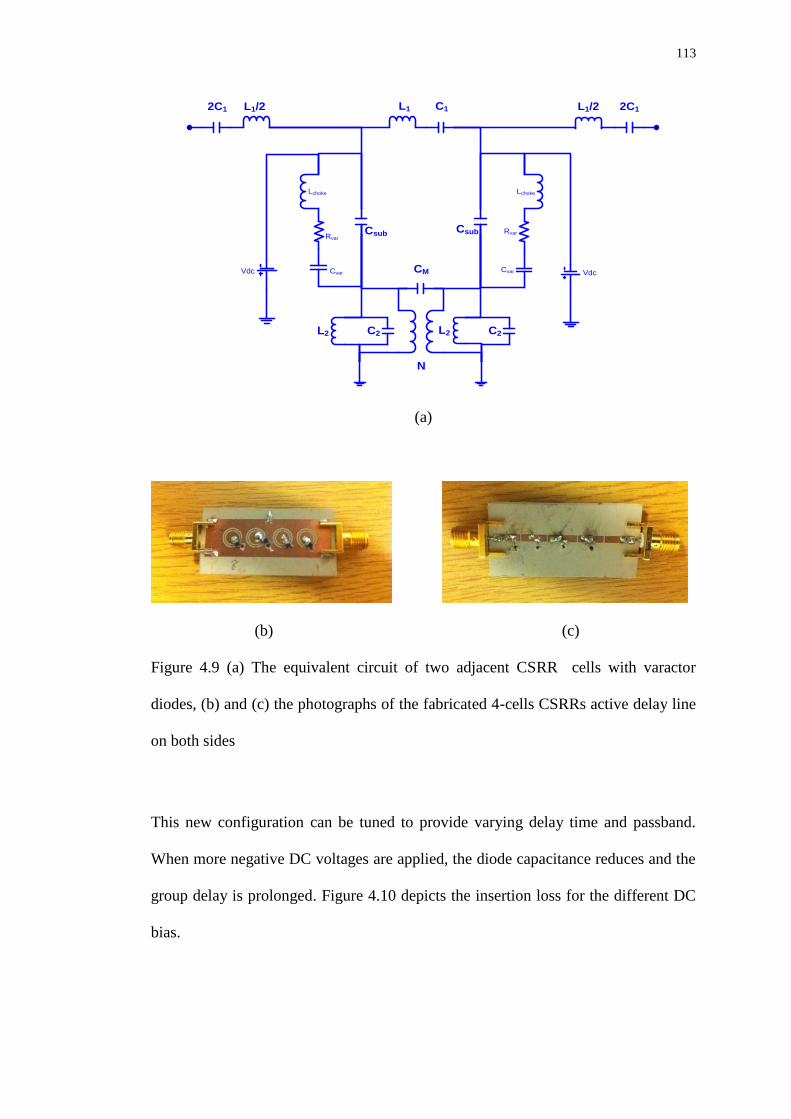
113
L1/2 L1
L2
2C1 C1
Csub
CM
C2
L1/2
L2
2C1
Csub
C2
N
Rvar
Cvar
Lchoke
Vdc
Rvar
Cvar
Lchoke
Vdc
(a)
(b) (c)
Figure 4.9 (a) The equivalent circuit of two adjacent CSRR cells with varactor
diodes, (b) and (c) the photographs of the fabricated 4-cells CSRRs active delay line
on both sides
This new configuration can be tuned to provide varying delay time and passband.
When more negative DC voltages are applied, the diode capacitance reduces and the
group delay is prolonged. Figure 4.10 depicts the insertion loss for the different DC
bias.

114
Figure 4.10 The insertion response (dB) after DC bias voltages of 4-cell CSRRs TL
The measured delay time, of the tunable delay line, for DC bias voltages is illustrated
in Figure 4.11. By observing a specific carrier frequency of 2.03GHz, it can be seen
that the diodes begin to have significant effects as the DC bias varied from -10V to -
20V. The DC changes the delay from 0.6ns to 5.6ns. However, owing to the diode
addition, which leads to the changing of the characteristic impedance, it is also
observed that the passband of CSRRs TL has moved toward higher frequencies and
suffered from addition loss due to the inherit diode properties, as illustrated in Figure
4.10.
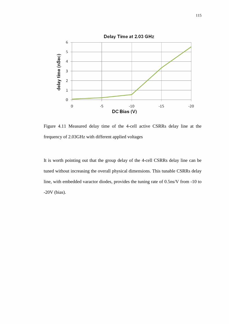
115
Figure 4.11 Measured delay time of the 4-cell active CSRRs delay line at the
frequency of 2.03GHz with different applied voltages
It is worth pointing out that the group delay of the 4-cell CSRRs delay line can be
tuned without increasing the overall physical dimensions. This tunable CSRRs delay
line, with embedded varactor diodes, provides the tuning rate of 0.5ns/V from -10 to
-20V (bias).
116
4.4 Conclusion
In this chapter, the 2 types of CSRRs delay line have been presented; the passive
CSRRs delay lines and the active CSRRs delay line.
In passive CSRRs delay lines, the compact model, consisting of 4-cell CSRRs
particle, has been demonstrated. It is found that the group delay of 4-cell CSRRs TL,
are dependent on the frequencies over the left-handed passband. Then, the two
waveforms, represented as the continuous wave and digital signal, are investigated,
in order, to verify the signal delays in CSRRs TL and group delays. The measured
results confirmed the group delays of LH passband are related as a function of
frequency. The 35mm length of 4-cell CSRRs delay line displays the delay of signal
2.25GHz modulated pulse, at 6ns and 2.5GHz modulated pulse, at 5ns, relating to
the group delay graph, respectively. In addition, the 35mm long 4-cell CSRRs TL is
presented 3ns delay at 2.3GHz which is approximately 10 times higher than those
can be provided by a conventional TL with the same length, which means the shorter
TL can be used in the system to obtain the same delay as in conventional case.
The later remarkable point in this work is the experimental demonstration of the
tunable delay line by embedding varactor diodes into the model of 4-cell CSRRs TL.
When DC bias varies from -10V to -20V, the average tuning rate 0.5ns/V is
presented. Even though, this method leads to the mismatching of characteristic
impedance of transmission line, the loading of varactor diode can make a large
change of group delay with compact size, which can be proved very useful especially
in for various radar and communications.

117
4.5 References
[4.1] A. R. Eskandari, and L. Mohammadi, “Group Delay Variations in Wideband
Transmission Lines: Analysis and Improvenment”, International Journal of
Soft Computing and Engineering (IJSCE), Vol. 1, Issue 4, pp. 122-128, Sept
2011.
[4.2] S. Keser, and M. Mojahedi, “Broadband Negative Group Delay Microstrip
Phase Shifter Design”, Antenna and Propagation Society International
Symposium 2009 (APSURSI’09), 978-1-4244-3647-7/09IEEE.
[4.3] S. Park, H, Choi, and Y. Jeong, ”Microwave Group Delay Time Adjuster”,
IEEE Microwave and Wireless Components Letters, Vol. 17, No. 2, pp. 109-
111, Feb 2007.
[4.4] H. T. Su, Y. Wang, F. Huang, and J. Michael, “Wide-Band Superconducting
Microstrip Delay Line”, IEEE transactions on Microwave Theory and
Techniques, Vol. 52, No. 11, pp. 3482-3487, Nov 2004.
[4.5] S. –K. Park, J. –K. Lee, and C. –D. Kim, “Group Delay Adjuster Using
Resonance Circuit with Varactor Diode”, APMC2005, 0-7803-9433-
X/05IEEE.
[4.6] J. –P. Castera, “State of the art in design and technology of MSW devices”,
Journal of Applied Physics 55(6), pp. 2506-2511, Mar 1984.
[4.7] H. Nakase, T. Kasai, and K. Tsubouchi, “On Chip Demodulator Using RF
Front-End SAW Correlator for 2.4 GHz Asynchronous Spread Spectrum
Modem”, PIMRC’94, EE33, pp. 374-378, E33, IEEE.
118
[4.8] E. R. Hirst, W. L. Xu, J. E. Bronlund ,and Y. J. Yuan, “Surface Acoustic
Wave Delay Line for Biosensor Application”, 15th
International conference
on Mechtronics and Machine Vision in Practice (M2VIPO8), pp. 40-44,
Auckland, NewZealand, Dec 2008.
[4.9] S. Gupta, A. Parsa, and C. Caloz, ”Group-Delay Engineered
Noncommensurate Transmission Line All-Pass Network for Analog Signal
Processing”, IEEE Transactions on Microwave Theory and Techniques, Vol.
58, No. 9, pp. 2392-2407, Sept 2010.
[4.10] C. Caloz and S. Gupta, “Analog Signal Processing in Transmission Line
Metamaterial Structures”, Radioengineering, Vol. 18, No. 2, pp. 155-167,
June 2009.
[4.11] H. V. Nguyen, and C. Caloz, “CRLH Delay Line Pulse Position Modulation
Transmitter”, IEEE Microwave and Wireless Components Letters, Vol. 18,
No. 8, pp. 527-529, Aug 2008.
[4.12] J. S. Diaz, A. A. Meleon, S. Gupta, and C. Caloz, “Impulse regime CRLH
resonator for tunable pulse rate multiplication”, Radio Science, Vol. 44,
RS4001, doi:10.1029/2008RS003991, 2009.
[4.13] S. Abielmona, S. Gupta, and C. Caloz, “Experimental Demonstration and
Characterization of a Tunable CRLH Delay Line System for
Impulse/Continuous Wave”, IEEE Microwave and Wireless Components
Letters, Vol. 17, No. 12, pp. 864-866, Dec 2007.
119
[4.14] S. Abielmona, S. Gupta, and C. Caloz, “Compressive Receiver Using a
CRLH-Based Dispersive Delay Line for Analog Signal Processing”, IEEE
Transaction of Microwave Theory and Techniques, Vol. 57, No. 11, pp.
2617-2626, Nov 2009.
[4.15] S. Haykin and M. Moher, COMMUNICATION SYSTEMS, 5th
edition, J.
Wiley& Sons, Inc., International student version, 2010.
[4.16] F. R. Connor, WAVE TRANSMISSION, 1st edition, Edward Arnold Ltd. 1972.
[4.17] D. M. Pozar, MICROWAVE ENGINEERING, 3rd
edition, J. Wiley& Sons,
Inc. 2005.
[4.18] N. J. Cronin, MICROWAVE AND OPTICAL WAVEGUIDE, IOP Publishing
Ltd. 1995.
[4.19] L. Ibbotson, THE FUNDAMENTALS OF SIGNAL TRANSMISSION: IN
LINE, WAVEGUIDE, FIBRE AND FREE SPACE, London Arnold 1999.
[4.20] PASAKAWEE, S. and HU, Z.: “Left-Handed Delay Line Implemented by
Complementary Split Ring Resonators (CSRRs)”, Asia Pacific Microwave
Conference, 2009.
[4.21] CALOZ, C. and ITOH, T.: “Transmission Line Approach of Left-Handed
(LH) Materials and Microstrip Implementation of an Artificial LH
Transmission Line”, IEEE Transactions on Antennas and Propagation,
Vol.52, No.5, pp. 1159-1166, May 2004.
[4.22] V. Radonic, B. Jokanovic, and V. C. Bengin, “Different Approaches to the
Design of Metamaterials”, Microwave Review, Dec 2007.

120
[4.23] W. Tang, and H. Kim, ”Compact Tunable Large Group Delay Line”,
Microwave and Optical Technology Letters, Vol. 51, No. 12, pp. 2893-2895,
Dec 2009.
[4.24] Y. –M. Park and D. –W. Kim, “Tunable Composite Right/Left-Handed Delay
Line with Large Group Delay for an FMCW Radar Transmitter”, Journal of
Electromagnetic Engineering and Science, vol. 12, No. 2, pp. 166-170, Jun
2012.

121
CHAPTER 5
FILTER THEORY AND ITS APPLICATION WITH CSRRS
INTRODUCTION
Wireless communication has been an important role in human’s life for the last few
decades. Owing to the rapid growth of communication technologies, there have been
many researches to develop devices and circuits for its applications in multiple
frequency bands [5.1-5.5]. In addition, the requirement of reducing interference
between channels must be met for all communication systems. Microwave filter is an
essential part to get rid of unwanted signal from the system and allow the signal in
specific frequency to pass through. Planar filters are widely used because of the
convenience in manufacturing, low profile and ease to apply with microwave
integrated circuits.
It is essential to design compact filters with high frequency selectivity, high rejection
at the band edge as well as wide rejection band. To achieve these demands, many
design techniques have been reported [5.6-5.11, 5.17, 5.18]. Since resonators are the
basic components of planar filters and from the view point of this filter design
section, filters with CSRRs have been introduced to accomplish above requirements
[5.12, 5.13, 5.19-5.22]. Generally, CSRRs with microstrip line presents the narrow
band properties [5.14-5.16]. In addition, CSRRs on microstrip line with a series gap
presents a passband frequency [5.27]. For this reason, a key contribution of this
122
Chapter is to provide microstrip wideband filters in L-Band frequency spectrum
from 0.9-1.9GHz with good frequency selectivity by the aid of rectangular CSRRs
and their coupling properties.
5.1 Definitions and Fundamentals of Filters
As mention above, filters are presented as a very essential component in radio
transmitter/receiver systems for recovery signals. On other words, it can be defined
as “a transducer for separating waves on the basis of their frequencies”. There are 3
main types of filter; Active filter (need external source for operating), passive filter
(no requiring external source for operating), and hybrid filter [5.23]. The two-port
network and lumped elements have been used to distribute filters and their frequency
responses [5.1, 5.23, 5.24].
5.1.1 2-port network analysis
Most RF/microwave components can be represented by a two-port network as shown
in Figure 5.1. The various parameters have been used to analyze the two-port
network, for instance; network variables, scattering parameters(S-parameters), and
short-circuit admittance parameters (Y-parameters), open-circuit impedance
parameters (Z-parameters), and ABCD parameters. These parameters can be
converted to each other. The S-parameters are used to present in this section which
are comprised of:
The Input Reflection Coefficient with the output port terminated by a
matched load or S11 (Return loss)
The Forward Transmission (insertion) gain with the output port terminated in
a matched load or S21 (Insertion loss)

123
The Reverse Transmission (insertion) gain with the input port terminated in a
matched load or S12
The Output Reflection Coefficient with the input terminated by a matched
load or S22
Figure 5.1 Two-port network with the input reflection coefficient and the output
reflection coefficient [5.1].
The 2 port network, shown in Figure 5.1, has the parameters V1, V2 and I1, I2 which
are voltage and current variables in complex amplitudes at port 1 and port 2,
respectively. Z01 and Z02 are the terminal impedances and Vs is the voltage generator.
At port1, the sinusoidal voltage is given by [5.1]
( )
1 1 1( ) cos( ) j tV t V t V e (5.1)
Therefore, the complex amplitude can be given by
1 1
jV V e (5.2)
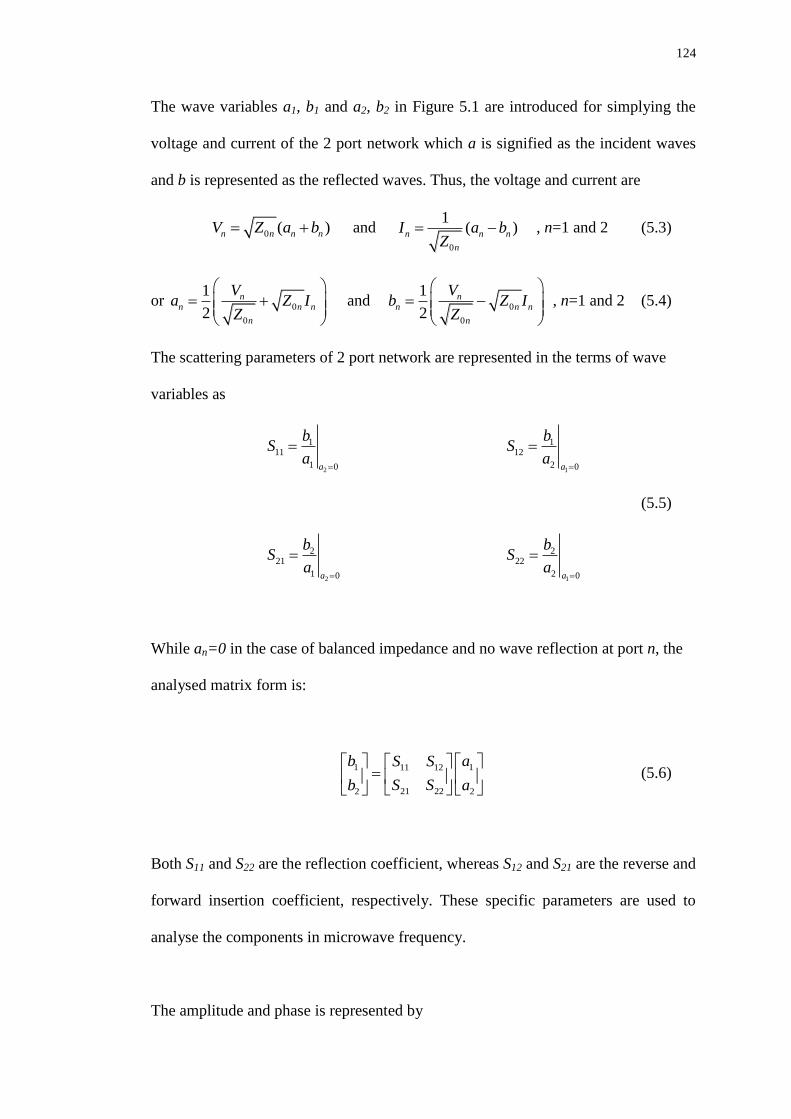
124
The wave variables a1, b1 and a2, b2 in Figure 5.1 are introduced for simplying the
voltage and current of the 2 port network which a is signified as the incident waves
and b is represented as the reflected waves. Thus, the voltage and current are
0 ( )n n n nV Z a b and 0
1( )n n n
n
I a bZ
, n=1 and 2 (5.3)
or 0
0
1
2
nn n n
n
Va Z I
Z
and 0
0
1
2
nn n n
n
Vb Z I
Z
, n=1 and 2 (5.4)
The scattering parameters of 2 port network are represented in the terms of wave
variables as
2
111
1 0a
bS
a
1
112
2 0a
bS
a
(5.5)
2
221
1 0a
bS
a
1
222
2 0a
bS
a
While an=0 in the case of balanced impedance and no wave reflection at port n, the
analysed matrix form is:
1 111 12
21 222 2
b aS S
S Sb a
(5.6)
Both S11 and S22 are the reflection coefficient, whereas S12 and S21 are the reverse and
forward insertion coefficient, respectively. These specific parameters are used to
analyse the components in microwave frequency.
The amplitude and phase is represented by
125
mnj
mn mnS S e
while m and n are the integer 1,2,… (5.7)
The amplitude is normally consider in dB from 20log mnS
While the insertion loss between port n and m (LA) and return loss at the port n (LR)
are
20log ...A mnL S m n (5.8)
20logR mnL S (5.9)
Which the return loss is related to the proportion of the Voltage Standing Wave
Ratio (VSWR) by
1
1
mn
mn
SVSWR
S
(5.10)
Beside the scattering parameters are used for microwave filter design, there are other
two paramters that use for analyzing the design. First, the Phase Delay (τp) represents
the difference phase of the wave between the input and output port in 2-port
network:
21p
(5.11)
Another one is the Group Delay (τd) which is considered the difference phase of the
baseband wave on the input port and output port:

126
21d
d
d
(5.12)
In 2-port network, The reflection parameter (S11) can be analized in the term of
terminal impedance (Z01) by replacing with Zin1=V1/I1. Zin1 is called the input
impedance by looking into port1, then
2
1 01 1 01111
1 1 01 1 010
/
/a
V Z I ZbS
a V Z I Z
(5.13)
V1 is replaced by Zin1I1, therefore
1 0111
1 01
in
in
Z ZS
Z Z
(5.14)
In the same means, if consider the port 2 as the input and Zin2=V2/I2, Zin2 is the input
impedance looking into port2.
2 0222
2 02
in
in
Z ZS
Z Z
(5.15)
In balanced network, The relation of S-parameters are
S12=S21 and S11=S22 (5.16)
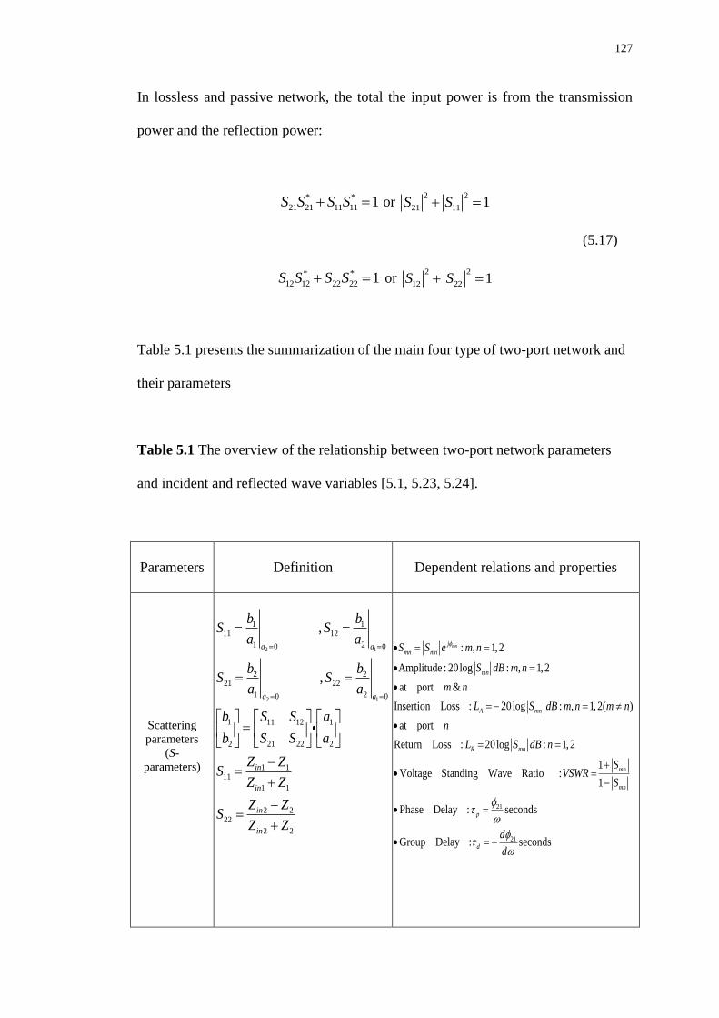
127
In lossless and passive network, the total the input power is from the transmission
power and the reflection power:
* *
21 21 11 11 1S S S S or 2 2
21 11 1S S
(5.17)
* *
12 12 22 22 1S S S S or 2 2
12 22 1S S
Table 5.1 presents the summarization of the main four type of two-port network and
their parameters
Table 5.1 The overview of the relationship between two-port network parameters
and incident and reflected wave variables [5.1, 5.23, 5.24].
Parameters
Definition
Dependent relations and properties
Scattering
parameters
(S-
parameters)
2 1
2 1
1 111 12
1 20 0
2 221 22
1 20 0
1 11 12 1
21 22 22
1 111
1 1
2 222
2 2
,
,
a a
a a
in
in
in
in
b bS S
a a
b bS S
a a
b S S a
S S ab
Z ZS
Z Z
Z ZS
Z Z
21
: , 1, 2
Amplitude : 20log : , 1,2
at port &
Insertion Loss : 20log : , 1,2( )
at port
Return Loss : 20log : 1,2
1Voltage Standing Wave Ratio :
1
Phase Delay : s
mnj
mn mn
mn
A mn
R mn
mn
mn
p
S S e m n
S dB m n
m n
L S dB m n m n
n
L S dB n
SVSWR
S
21
econds
Group Delay : secondsd
d
d
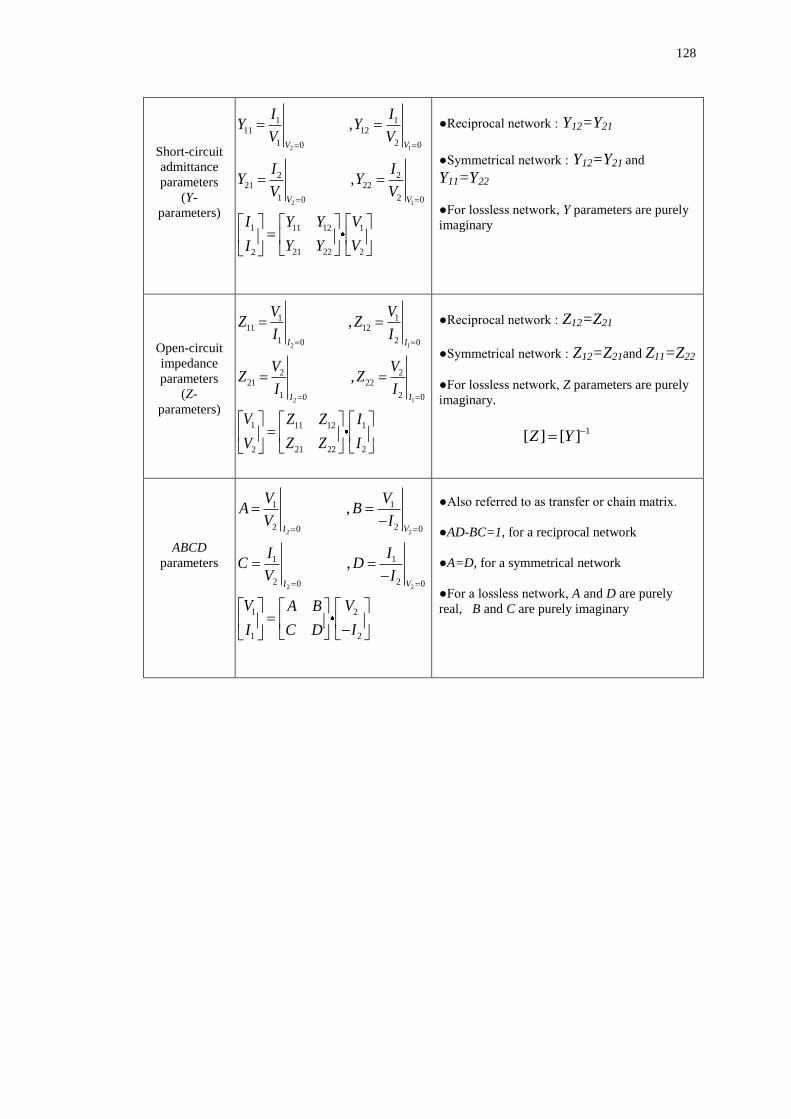
128
Short-circuit
admittance
parameters
(Y-
parameters)
Reciprocal network : Y12=Y21
Symmetrical network : Y12=Y21 and
Y11=Y22
For lossless network, Y parameters are purely
imaginary
Open-circuit
impedance
parameters
(Z-
parameters)
Reciprocal network : Z12=Z21
Symmetrical network : Z12=Z21and Z11=Z22
For lossless network, Z parameters are purely
imaginary.
ABCD
parameters
Also referred to as transfer or chain matrix.
AD-BC=1, for a reciprocal network
A=D, for a symmetrical network
For a lossless network, A and D are purely
real, B and C are purely imaginary
1[ ] [ ]Z Y
2 1
2 1
1 111 12
1 20 0
2 221 22
1 20 0
1 11 12 1
21 22 22
,
,
I I
I I
V VZ Z
I I
V VZ Z
I I
V Z Z I
Z Z IV
2 2
2 2
1 1
2 20 0
1 1
2 20 0
1 2
21
,
,
I V
I V
V VA B
V I
I IC D
V I
V VA B
II C D
2 1
2 1
1 111 12
1 20 0
2 221 22
1 20 0
1 11 12 1
21 22 22
,
,
V V
V V
I IY Y
V V
I IY Y
V V
I Y Y V
Y Y VI
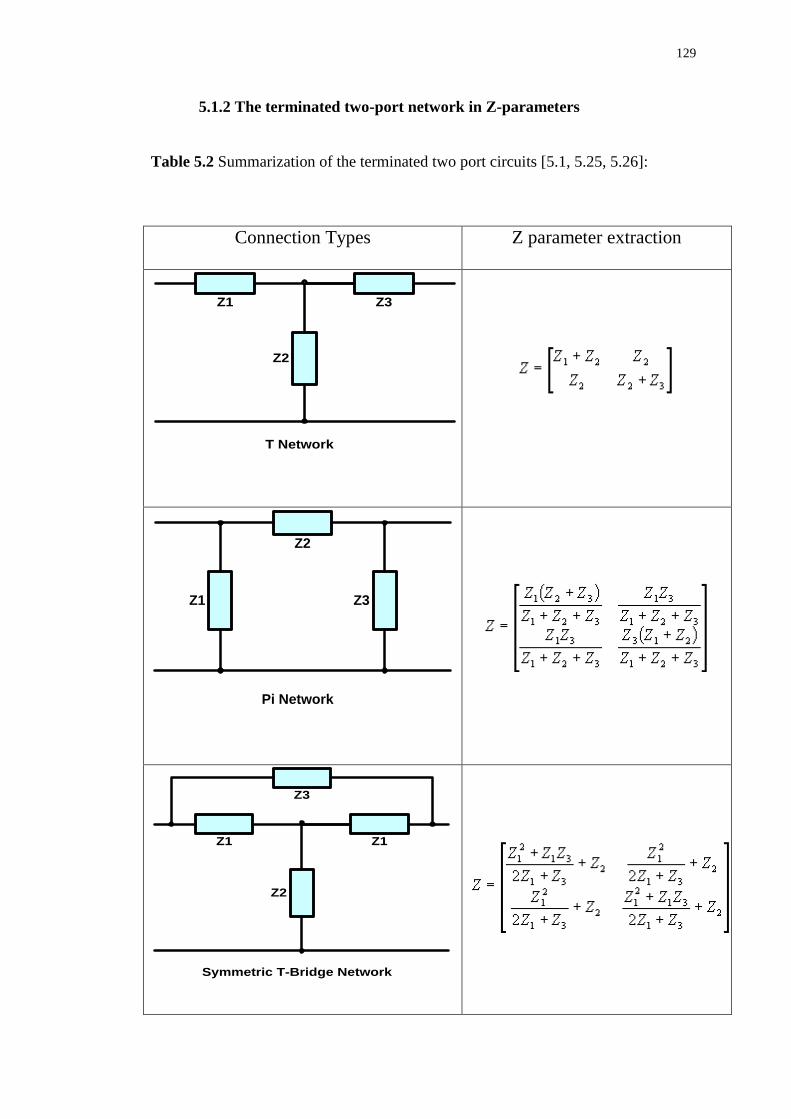
129
5.1.2 The terminated two-port network in Z-parameters
Table 5.2 Summarization of the terminated two port circuits [5.1, 5.25, 5.26]:
Connection Types Z parameter extraction
Z3Z1
Z2
T Network
Z2
Z1
Pi Network
Z3
Z3
Z1Z1
Z2
Symmetric T-Bridge Network

130
Z2
Z1
Symmetric Lattice Network or
Symmetric X Network
Z1
Z2
5.1.3 The interconnection of two-port circuits
The 2 port networks can be connected as in Figure 5.2 [5.26]:
Z1
Z2
I1
V2
I2
V1
(a) Series connection of two 2-port networks: Z=Z1+Z2
Y1
Y2
I1
V1
I2
V2
(b) Parallel connection of two 2-port networks: Y=Y1+Y2

131
A1 A2
I1
V1
I2
V2
(c) Cascade connection of two 2-port networks: A=A1A2
Figure 5.2 Interconnection of two-port network (a) Series, (b) Parallel, and (c)
Cascade [5.26]
If the 2 port networks with Z-parameters are connected in series, the equivalent port
is given by
[Z]eq=[Z]1+[Z]2+[Z]3…+[Z]n , n is the number of 2 port network with Z-parameters
If the 2 port networks with Y-parameters are connected in parallel, the equivalent
port is
[Y]eq=[Y]1+[Y]2+[Y]3…+[Y]n , n is the number of 2 port network with Y-parameters
If the 2 port networks are connected in cascade which each individual networks have
transmission parameters [A]1, [A]2, [A]3,…,[A]n, the total equivalent 2 port
parameter will have a transmission parameter by
[A]eq= [A]1*[A]2* [A]3*…*[A]n, n is the number of each individual network
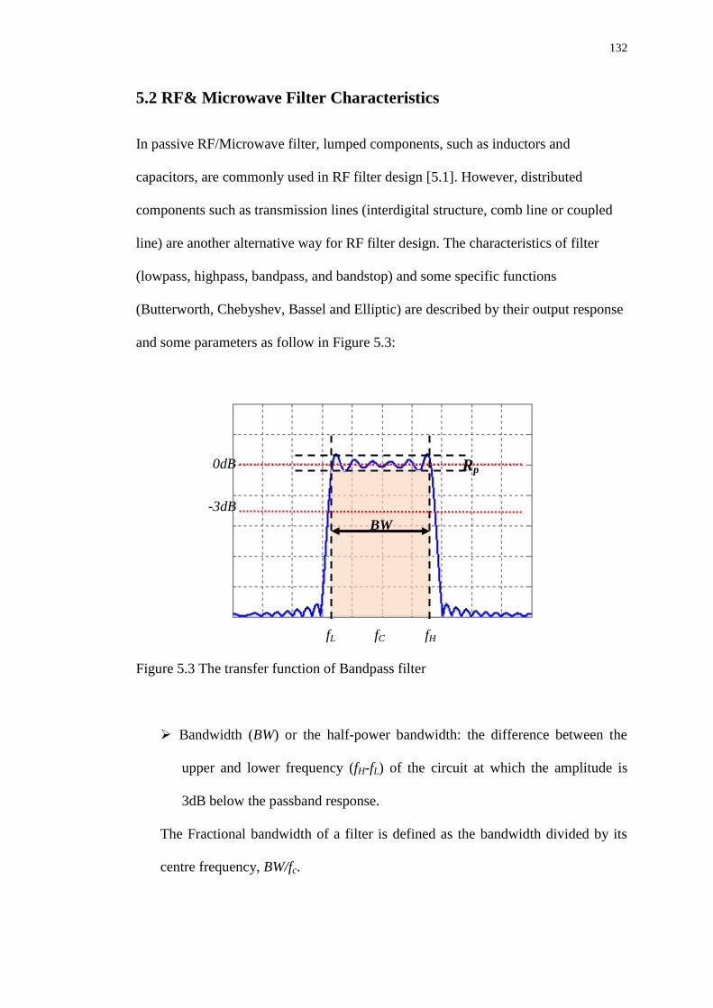
132
5.2 RF& Microwave Filter Characteristics
In passive RF/Microwave filter, lumped components, such as inductors and
capacitors, are commonly used in RF filter design [5.1]. However, distributed
components such as transmission lines (interdigital structure, comb line or coupled
line) are another alternative way for RF filter design. The characteristics of filter
(lowpass, highpass, bandpass, and bandstop) and some specific functions
(Butterworth, Chebyshev, Bassel and Elliptic) are described by their output response
and some parameters as follow in Figure 5.3:
Figure 5.3 The transfer function of Bandpass filter
Bandwidth (BW) or the half-power bandwidth: the difference between the
upper and lower frequency (fH-fL) of the circuit at which the amplitude is
3dB below the passband response.
The Fractional bandwidth of a filter is defined as the bandwidth divided by its
centre frequency, BW/fc.
fL fC fH
0dB
-3dB
BW
Rp

133
Ripple (RP): in frequency domain is the periodic variation of insertion loss,
normally knows as the difference between the maximum and minimum of
the insertion loss in passband.
Insertion loss (IL): the loss of signal in power after transmitted to device,
normally presented in dB as 10log (PT/PR), where as PT is the beginning
power transmitted in to the load and PR is the power received by load. In
scattering parameter, the insertion loss ( ) is defined as
:
20log 21IL S dB
Return loss (RL): the difference in dB between the forward and reflected
power measured at the output point of filter.
Selectivity: the desired attenuation of the unwanted frequencies. In filter
design, filter’s selectivity defines how much the filter will reject unwanted
frequencies.
Q factor: The inverse fractional bandwidth defined as cfQBW
; a high Q
filter gives narrow passband, while a low Q filter will have a wide passband.
Group delay: is the amount of time for signal to pass through the filter, most
types of filter the group delay is defined as dϕ/df varied with frequency.
5.3 Overview of the Design Filter
There are many methods to design RF/microwave filters. Because of the high
efficiency, easy manufacture, the coupling techniques are recommended, especially
in planar filters [5.4-5.11]. In this chapter, a high rejection in the lower band and
improved wideband pass filters are designed using CSRRs and coupling stub
arrangement. The two main parts of this design are
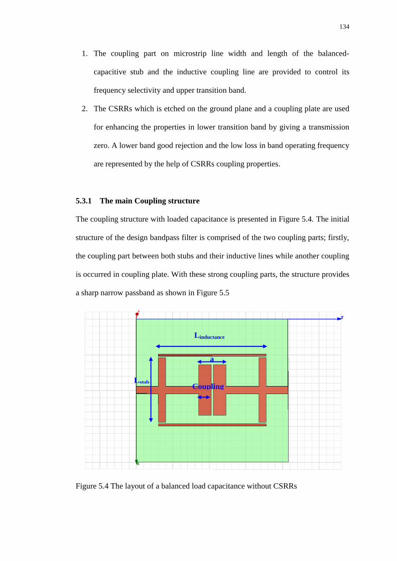
134
1. The coupling part on microstrip line width and length of the balanced-
capacitive stub and the inductive coupling line are provided to control its
frequency selectivity and upper transition band.
2. The CSRRs which is etched on the ground plane and a coupling plate are used
for enhancing the properties in lower transition band by giving a transmission
zero. A lower band good rejection and the low loss in band operating frequency
are represented by the help of CSRRs coupling properties.
5.3.1 The main Coupling structure
The coupling structure with loaded capacitance is presented in Figure 5.4. The initial
structure of the design bandpass filter is comprised of the two coupling parts; firstly,
the coupling part between both stubs and their inductive lines while another coupling
is occurred in coupling plate. With these strong coupling parts, the structure provides
a sharp narrow passband as shown in Figure 5.5
Figure 5.4 The layout of a balanced load capacitance without CSRRs
a
Lstub
Linductance
Coupling
plate
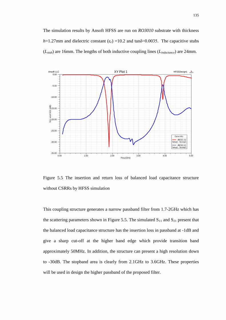
135
The simulation results by Ansoft HFSS are run on RO3010 substrate with thickness
h=1.27mm and dielectric constant (εr) =10.2 and tanδ=0.0035. The capacitive stubs
(Lstub) are 16mm. The lengths of both inductive coupling lines (Linductance) are 24mm.
0.00 1.00 2.00 3.00 4.00 5.00Freq [GHz]
-35.00
-30.00
-25.00
-20.00
-15.00
-10.00
-5.00
0.00
S1
1 a
nd
S2
1 (
dB
)
Ansoft LLC HFSSDesign1XY Plot 1 ANSOFT
Curve Info
dB(S(1,1))Setup1 : Sw eep1
dB(S(2,1))Setup1 : Sw eep1
Figure 5.5 The insertion and return loss of balanced load capacitance structure
without CSRRs by HFSS simulation
This coupling structure generates a narrow passband filter from 1.7-2GHz which has
the scattering parameters shown in Figure 5.5. The simulated S11 and S21 present that
the balanced load capacitance structure has the insertion loss in passband at -1dB and
give a sharp cut-off at the higher band edge which provide transition band
approximately 50MHz. In addition, the structure can present a high resolution down
to -30dB. The stopband area is clearly from 2.1GHz to 3.6GHz. These properties
will be used in design the higher passband of the proposed filter.

136
5.3.2 Electromagnetic Properties of CSRRs
The rectangular CSRRs loaded transmission line and its equivalent circuit model
have been present [5.14-5.16], shown on Figure 5.6(a) and (b).
(a)
L/2 L/2
Lr
Cc
Cr
2Cg 2Cg
(b)
Figure 5.6 (b) The unit cell of CSRRs loaded with transmission line topology and (b)
its equivalent circuit [5.14-5.16]
Figure 5.6(a) represents the topology of rectangular CSRRs which is composed of
the three factor as following air slot on ground plane (d), its conductance (c), and the
dimension length (a), respectively. Owing to the behavior of CSRRs which acts as
LC resonator, the equivalent circuit can be modeled by these following parameters:
CSRRs is formed by the parallel combination of Lr and Cr and its coupling to the
host line is represented by the capacitance Cc. The series gap on transmission line is
represented by Cg.

137
As a result of input port at the resonant frequency, the parameter L and Cg can be
ignored. Therefore, the intrinsic resonant frequency of CSRRs is given by [14-16]
1
2r
r r
fL C
(5.18)
The transmission zero is given by
1
2 ( )Z
r c r
fL C C
(5.19)
From equation (5.18) and (5.19), CSRRs has been applied in this design model for
selecting the passband of filter and controlling the transmission zero which is related
to a high rejection in the lower band.
5.3.3 Combination model of the microstrip coupling structure and CSRRs
As previous mentioned, this research presents a new configuration of wideband filter
under the perspective of metamaterials in microstrip configuration by using the
rectangular complementary split-ring resonators (CSRRs). The design technique of
this filter is based on combining of rectangular CSRRs on ground plane and the
coupling structure formed by microstrip line on Figure 5.4. The layout of proposed
filter is shown in Figure 5.7.

138
(a)
(b)
Figure 5.7 The layout of proposed filter. (a) Basic cell, (b) Topology of rectangular
CSRRs
The width of strip (W) and stubs (Wstub) are 2mm while the lengths of balanced
inductive stubs (Lstub) are 14mm which is the same length as coupling plate,
respectively. The width of coupling plate is 4mm. The length of both inductance
lines (Linductance) is 29.5mm, whereas their width (Winductance) is 0.3mm and all gaps
are maintained at 0.3mm, respectively. The rectangular CSRRs size (a) is 10mm.
a
Lstub
Linductance
Coupling plate
a

139
(a) at frequency 0.72GHz (b) at frequency 1.4GHz
Figure 5.8 The current distributions of the proposed bandpass filter at (a) 0.72GHz
(no transmission) (b) 1.4GHz (centre frequency), respectively
As shown in Figure 5.8(a), the unwanted signal is reflected, hence no current is
transferred to port2 on the transmission zero frequency at 0.72GHz. At 1.4GHz
which is in the passband of the proposed filter, the wanted signal has been
propagated to port2, illustrated in Figure 5.8(b).
(a) at frequency 0.72GHz (b) at frequency 1.4GHz
Figure 5.9 The magnetic field distribution on ground plane at (a) 0.72GHz and (b)
1.4GHz, respectively
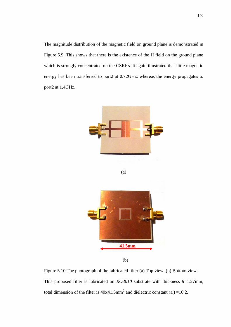
140
The magnitude distribution of the magnetic field on ground plane is demonstrated in
Figure 5.9. This shows that there is the existence of the H field on the ground plane
which is strongly concentrated on the CSRRs. It again illustrated that little magnetic
energy has been transferred to port2 at 0.72GHz, whereas the energy propagates to
port2 at 1.4GHz.
(a)
(b)
Figure 5.10 The photograph of the fabricated filter (a) Top view, (b) Bottom view.
This proposed filter is fabricated on RO3010 substrate with thickness h=1.27mm,
total dimension of the filter is 40x41.5mm2 and dielectric constant (εr) =10.2.
41.5mm
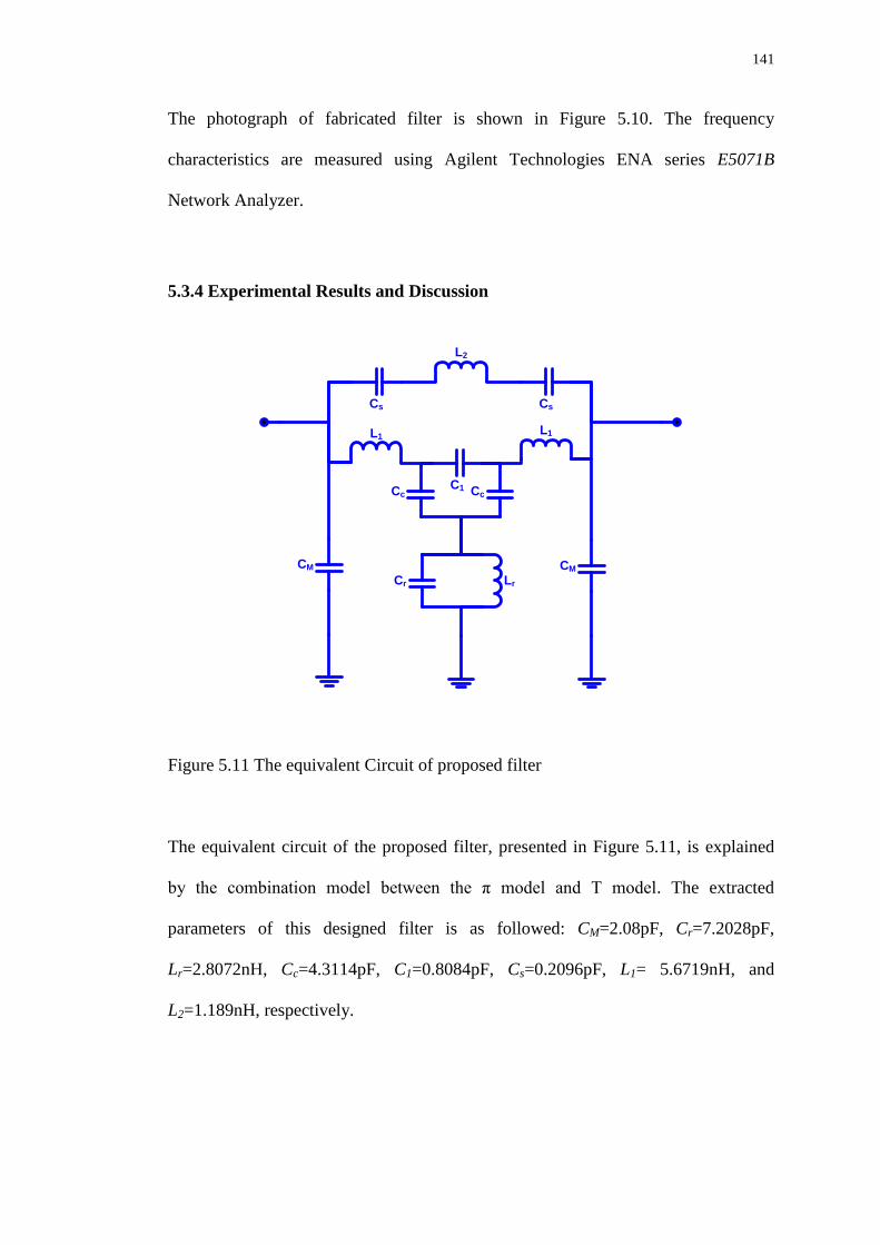
141
The photograph of fabricated filter is shown in Figure 5.10. The frequency
characteristics are measured using Agilent Technologies ENA series E5071B
Network Analyzer.
5.3.4 Experimental Results and Discussion
L2
Cs Cs
C1Cc Cc
L1L1
CM CM
Cr Lr
Figure 5.11 The equivalent Circuit of proposed filter
The equivalent circuit of the proposed filter, presented in Figure 5.11, is explained
by the combination model between the π model and T model. The extracted
parameters of this designed filter is as followed: CM=2.08pF, Cr=7.2028pF,
Lr=2.8072nH, Cc=4.3114pF, C1=0.8084pF, Cs=0.2096pF, L1= 5.6719nH, and
L2=1.189nH, respectively.

142
(a).
(b)
Figure 5.12 The ADS simulated S-parameters (a), and (b) comparison of ADS and
HFSS simulated frequency responses on the designed filter at 0.9-1.9GHz.
The equivalent circuit simulated results of the proposed filter is shown in Figure
5.12(a). In Figure 5.12(b), the comparison of the two simulated results by ADS
equivalent circuit and HFSS are illustrated. Reasonably good agreements can be
found in the two simulated results. However, there are some discrepancies. The

143
equivalent circuit analysis provides wider band and lower transmission zero. This is
because the equivalent circuit analysis cannot provide the total effects from magnetic
loss tangents, substrate loss, and measurement loss, etc.
Figure 5.13 shows the simulated and measured results of the return loss S11 and
insertion loss S21 in wideband. The results of the frequency response measured on
the fabricated band pass filter substrate show satisfactory agreement with the
simulated frequency responses by the HFSS in the region of interest.
Figure 5.13 Measured and HFSS simulated frequency response on the designed filter
at 0.9-1.9GHz.
The measured insertion loss is about 0.9dB at the centre frequency and the passband
return loss is less than -10dB. The filter presents wideband properties which covers
the frequencies from 0.9 to 1.9GHz. The 3dB FBW is approximately 77%. These

144
values are adequate enough to be used in communication channel filtering.
Moreover, it is noticed that the excellent characteristic of the out-of-band rejection
can be achieved due to the induced between a parallel inductive line coupling and the
rectangular CSRRs by obtaining up to 3.4GHz. This results show the effect of
applied CSRR on conventional filter that can be modified the filter properties
without changing a fundamental dimension. Owing to the CSRR properties, a sharp
transition band with transmission zero deep down to -60dB by measurement at the
lower cut-off edge is presented.
5.4 Conclusion
In this chapter, the design and fabrication of the wideband pass filter with the
bandwidth 1GHz based on the complementary split-ring resonators (CSRRs) have
been presented. It was found that the presence of CSRRs on conventional coupling
filter can modify the filter properties from 300MHz narrowband filter to 1GHz
wideband filter without changing any profile. In this work, the measured insertion
loss of this design filter at operation band is very low which presents <1dB at the
centre frequency as well as the passband return loss is less than -10dB. With CSRR
properties, the transmission zero and a sharp transition band on the lower cut-off
frequency has been demonstrated. At the out of band on higher frequency, this
proposed filter exhibits a frequency suppression which is occurred on the
conventional coupling filter at 3.9GHz. This design filter provides the excellent
characteristic of both in band and out of band.

145
5.5 References
[5.1] J. –S. Hong and M.J. Lancaster, Microstrip Filters for RF/Microwave
Applications, Wiley, New York, 2001.
[5.2] L. Zhang, Z. –Y. Yu, and S. –G. Mo, ”Novel Planar Multimode Bandpass
Filters with Radial-Line Stubs”, Progress In Electromagnetics Research,
PIER 101, 33-42, 2010.
[5.3] C. –Y Huang, Y. –X. Yu, and R. –Y. Yang, ”High Selective Dual-Band
Bandpass Filter design with Novel Feed Scheme”, Proceedings of the World
Congress on Engineering 2010 (WCE2010), Vol. II, London, Uk.
[5.4] P. Sarkar, R. Ghatak, and D. R. Poddar,”A Dual-Band Bandpass Filter Using
SIR Suitable for WiMAX Band”, 2011 International Conference on
Information and Electronic Engineering, IPCSIT press, Vol. 6, 2011.
[5.5] B. Xia, L. S. Wu, and J. F. Mao,”An Ultra-Wideband Balanced Bandpass
Filter Based on Defected Ground Structures”, Progress In Electromagnetics
Research C, Vol. 25, 133-144, 2012.
[5.6] J. S. Hong and M. J.,”Theory and Experiment of Novel Microstrip Slow-
Wave Open-Loop Resonator Filters”, IEEE Transactions on Microwave
Theory and Techniques, Vol. 45, No. 12, pp. 2358-2365, December 1997.
[5.7] S. S. Karthikeyan and R. S. Kshetrimayum, ”Compact, Deep, and Wide
Rejection Bandwidth Low-pass Filter using Open Complementary Split Ring
Resonator”, Microwave and Optical Technology Letters, Vol. 53, No.4, April
2011.
[5.8] A. Hasan and A. E. Nadeem,”Novel Microstrip Hairpinline Narrowband
Bandpass Filter Using Via Ground Holes”, Progress In Electromagnetics
Research, PIER 78, 393-419, 2008.

146
[5.9] M. N. Moghadasi and M. Alamolhoda,”Spurious Response Suppression in
Hairpin Filter using DMS Integrated in Filter Structure”, Progress In
Electromagnetics Research C, Vol. 18, 221-229, 2011.
[5.10] S. M. Wang, C. H. Chi, M. Y. Hsieh, and C. Y. Chang,”Miniaturized
Spurious Passband Suppression Microstrip Filter Using Meandered Parallel
Coupled Lines”, IEEE Transactions on Microwave Theory and Techniques,
Vol. 53, No. 2, pp. 747-753, February 2005
[5.11] R. Lerdwanittip, A. Namsang, and P. Akkaraektalin,”Bandpass Filters using
T-shape Stepped Impedance Resonators for Wide Harmonics Suppression
and their Application for a Diplexer”, Journal of Semiconductor Technology
and Science, Vol. 11, No. 1, March 2011.
[5.12] M. Keshvari and M. Tayarani, “A Novel Miniaturized Bandpass Filter Based
on Complementary Split Ring Resonators (CSRRs) and Open-Loop
Resonators”, Progress In Electromagnetics Research Letters, Vol.23, 165-
172, 2011.
[5.13] D. M. Choi, D. O. Kim, and C. Y. Kim,”Design of a Compact Narrow Band
Pass Filter Using the Rectangular CSRRs”, PIERS Online, Vol. 5, No.5,
2009.
[5.14] M. Gil, J. Bonache and F. Martin, ”On the transmission properties of left-
handed microstrip lines implemented by complementary split rings
resonators”, Int. J. Numer. Model, 19:87-103, 2006.
[5.15] J. C. Liu, H. C. Line, and D. C. Chang,”An Improved Equivalent Circuit
Model for CSRR-Based Bandpass Filter Design With Even and Odd Modes”,
IEEE Microwave and Wireless components letters, Vo. 20, No.4, April, 2010

147
[5.16] M. Gill, I. Gill, J. Bonache, and F. Martin,”Metamaterial transmission lines
with extreme impedance values”, Microwave and Optical Technology letters,
Vol. 48, No. 12, pp. 2500-2505, December 2006.
[5.17] S. Y. Lee and C. M. Tsai,”Design of microstrip filter using multiple
capacitively loaded coupled lines”, IET Microwave Antennas Propagation,
Vol. 1, pp. 651-657, June 2007.
[5.18] M. Chen, Y. C. Lin, and M. H. Ho,”Quasi-Lumped Design of Bandpass Filter
Using Combined CPW and Microstrip”, Progress In Electromagnetics
Research Letters, Vol. 9, 59-66, 2009.
[5.19] X. Lai, Q. Li, P. Y. Qin, B. Wu, and C. H. Liang,”A Novel Wideband
Bandpass Filter Based on Complementary Split-Ring Resonator”, Progress
In Electromagnetics Research C. Vol. 1, 177-184, 2008.
[5.20] A. Ali and Z. Hu,”Negative permittivity meta-material microstrip binomial
low-pass filter with sharper cut-off and reduced size”, IET Microwave &
Antenna Propagation, Vol. 2, No. 1, pp. 15-18, February 2008.
[5.21] J. Zhang, B. Cui, S. Lin, and X. W. Sun,”Sharp-Rejection Low-pass Filter
with Controllable Transmission Zero Using Complementary Split Ring
Resonators (CSRRs)”, Progress In Electromagnetics Research, PIER 69,
219-226, 2007.
[5.22] M. Keshvari and M. Tayarani,”A Novel Miniaturized Bandpass Filter based
on Complementary Split Ring Resonators (CSRRs) and Open-Loop
Resonators”, Progress In Electromagnetics Research Letters, Vol. 23, 165-
172, 2011.
[5.23] P. A. Rizzi, Microwave Engineering: Passive Circuits, Prentice Hall, 1988.
148
[5.24] D. M. Pozar, Microwave Engineering, John Wiley and Sons, Inc., 2nd
edition
1998.
[5.25] L. Zhu, S. Sun, and R. Li, Microwave Bandpass Filters for Wideband
Communications, John Wiley & Sons, 28 Dec 2011.
[5.26] A. Grebennikov, RF and Microwave Transmitter Design, John Wiley &
Sons, 21 Feb 2011.
[5.27] C. Li, K.-Y. Liu and F. Li,”Design of microstrip highpass filters with
complementary split ring resonators”, Electronics Letters, Vol.43, No.1, 4th
Jan 2007.
149
CHAPTER 6
ANTENNA THEORY AND APPLICATIONS WITH CSRRS
INTRODUCTION
The specific-electromagnetic properties of metamaterials, which give the negative
permeability and negative permittivity, have led to the first Split Ring Resonators
(SRRs) been reported by Pendry [6.1, 6.2]. There are many applications of
metamaterials, which have been applied in the last decade, including antennas, in
order to enhance their performance [6.3, 6.4]. Due to the properties of metamaterials
that can manipulate the electromagnetic field, the higher impedance substrate can be
generated. This can be used to reduce the size as well as maintain its efficiency.
This chapter mainly consists of three parts. The first part will briefly mention about
the basic microstrip patch antennas and its properties. The second part will present a
new technique of antenna size reduction, by etching CSRRs on the ground plane as
well as the inductively meander line loaded patch. By this method, the size reduction
of the proposed antenna can reach 74% of the conventional rectangular patch
antenna. In last part, the technique of tunable CSRRs antenna has been introduced by
reversely biasing the varactor diode between its patch and ground side. The wide
tuning range has been achieved to 350 MHz without changing any dimension. The
tunable CSRR microstrip antenna still remains compact.
150
6.1 Antenna Theory and its Definition
Antenna is one of the most crucial components in wireless communication systems.
The IEEE defines antenna as “The part of a transmitting or receiving system that is
designed to radiate or receive electromagnetic waves”. Webster’s Dictionary defines
antenna as “a usually metallic device (as a rod or wire) for radiating or receiving
radio waves”. In other words, antenna is a structure used to transit the signal between
free space and a guiding device e.g. transmission line. Then, transmission line will
transport electromagnetic energy from the antenna to the receiver or from the
transmitting source to the antenna [6.5].
Generally, there are two categories of antennas according to their application [6.5]:
Omnidirectional antennas are called the group that radiate or receive in all
directions. It is normally used when the relative position of the other station
is arbitrary or unknown.
Directional or beam antennas are used to specially receive or radiate in a
certain direction or directional pattern.
If consider in terms of type, antennas can be divided into various types such as wire
antennas, aperture antennas, lens antennas, reflector antennas, and microstrip patch
antennas [6.5].
151
6.1.1 Antenna Radiation and its Characteristic
An antenna radiates its signal which is occurred basically due to the time varying
(AC) current or acceleration of charge. It is simply said that without motion of
charges in a wire (no current), no radiation happens. The antenna radiation can be
explained in Figure 6.1 [6.5].
A voltage source, connected to a two conductor transmission line, applies a
sinusoidal voltage wave across the transmission line. A sinusoidal electric field is
generated which causes the appearance of electric lines of force which are tangential
of the electric field.
The electric field’s magnitude is shown by the high concentration of the electric line
of force. The movement of the free electrons on the conductors under the electric
lines of force leads to the appearance of current flow which forms a magnetic field.
The time varies of magnetic and electric fields will then create the electromagnetic
waves traveled between the conductors. The free space waves are appeared at the
open ends of the electric lines which is connected to the open space. Because the
electromagnetic waves are continuously generated by the sinusoidal wave from the
source, its electric disturbance is constant which leads to these waves can propagate
through the transmission line and the antenna as well as the free space radiating.
Owing to the charges, inside the transmission line and antenna part, the
electromagnetic waves are continuing upheld. While in the free space; they are
radiated after creating closed loops [6.5].
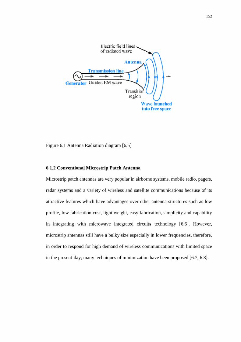
152
Figure 6.1 Antenna Radiation diagram [6.5]
6.1.2 Conventional Microstrip Patch Antenna
Microstrip patch antennas are very popular in airborne systems, mobile radio, pagers,
radar systems and a variety of wireless and satellite communications because of its
attractive features which have advantages over other antenna structures such as low
profile, low fabrication cost, light weight, easy fabrication, simplicity and capability
in integrating with microwave integrated circuits technology [6.6]. However,
microstrip antennas still have a bulky size especially in lower frequencies, therefore,
in order to respond for high demand of wireless communications with limited space
in the present-day; many techniques of minimization have been proposed [6.7, 6.8].

153
Figure 6.2 Microstrip Patch Antenna structure.
Generally, a microstrip patch antenna comprises of the feed lines and a radiating
patch, made of conducting material such as copper, on one side of a dielectric
substrate and has a ground plane on the other side. The example of a rectangular
microstrip patch antenna, shown in Figure 6.2, has the length L, width W placing on
a substrate of height h. The radiating patch can be of many shapes and size, for
example, rectangular, circular, elliptical, triangular or square etc. For a rectangular
patch, the length L of the patch is usually 2/3/ 00 L , where λ0 is the free-
space wavelength. The patch thickness (t) is chosen to be quite thin by t<< λ0. The
height h of the dielectric substrate is typically 0 00.003 0.05h . The dielectric
constants (εr) of substrate of the design microstrip antennas can be ranging from 2.2
to 12 [6.5].
The feeding method is an important factor which can affect the performance of the
design patch antenna. In the other words, the different feeding methods exhibit
Patch antenna
substrate
Feeding point
W
L
h
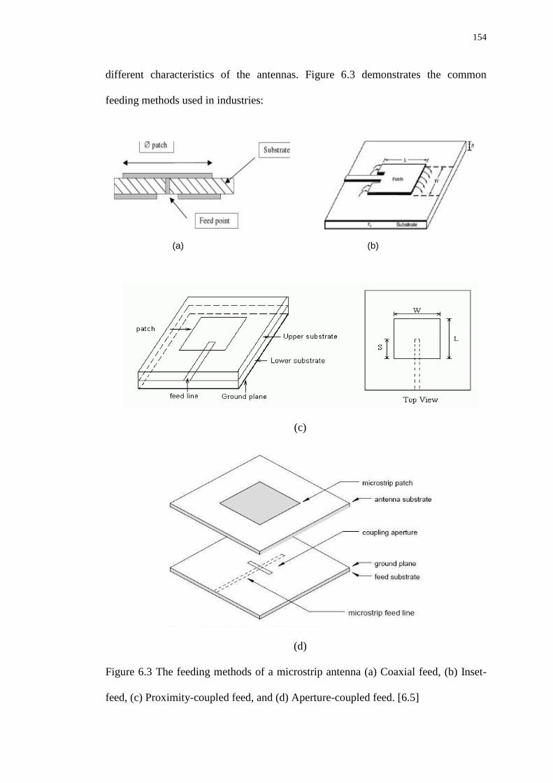
154
different characteristics of the antennas. Figure 6.3 demonstrates the common
feeding methods used in industries:
(a) (b)
(c)
(d)
Figure 6.3 The feeding methods of a microstrip antenna (a) Coaxial feed, (b) Inset-
feed, (c) Proximity-coupled feed, and (d) Aperture-coupled feed. [6.5]

155
The most common and easiest feed is coaxial type, while inset feed is widely used
for array antennas. The proximity-coupled feed is recommended to use for reducing
spurious radiation from the feed line in multilayer fabrication. The aperture-coupled
feed type, used in thick substrate, can eliminate feed line radiation [6.5, 6.6].
Patch antennas radiate mainly because of the fringing fields between the ground
plane and the edge of the patch. The antenna that has a thick dielectric substrate with
a low dielectric constant is desirable because it provides better efficiency, larger
bandwidth and better radiation; however, it has a larger size [6.5]. In order to design
a compact patch antenna, higher dielectric constants must be used which are less
efficient and result in narrower bandwidth. Compensation must be made between
antenna performance and dimensions while design an antenna.
6.1.3 The Advantages and Disadvantages of Microstrip Patch Antennas
Since 1950s, microstrip antennas have been widely used, as compared as the
conventional microwave antennas. Table 6.1 illustrates the gain of microstrip
antennas over the conventional microwave antennas [6.6];

156
Table 6.1 Comparison of microstrip antennas and conventional microwave antennas
Advantages
Disadvantages and limitations
Light weight, low volume and thin profile configurations
Low fabrication cost (readily amenable to mass production)
Compatible with printed-circuit technology (easy to manufacture as standalone elements or as arrays elements)
In case of very thin substrate, they may also be conformable such as bending that leads to unobtrusive antenna
Linear and circular polarizations can be applied with simple feed
Dual frequency and dual polarization antennas can be easily made
No cavity backing is required
Easily integrated with microwave integrated circuits
Feed lines and matching networks can be fabricated simultaneously with the antenna structure
Narrow bandwidth and associated tolerance problems
Some, lower gain (-6dB)
Larger ohmic loss in the feed structure of arrays
Most radiate into half-space
Complex feed structures required for high-performance arrays
Polarization purity is difficult to achieve
Poor end-fire radiator, except tapered slot antennas
Extraneous radiation from feeds and junctions
Lower power handing capability (approx. 100W)
Reduced gain and efficiency as well as unacceptably high levels of cross-polarization and mutual coupling within an array environment at high frequencies
Excitation of surface waves
Most fabricated on a high dielectric constant of substrate, leads to poor efficiency and narrow bandwidth
Lower radiation efficiency
Although microstrip antennas have these limitations, most can be minimized.
Several techniques have been proposed to overcome these limitations such as array
configuration techniques with power handling [6.9] and choke structure to gain the
limitation of surface-waves [6.10, 6.11], etc.
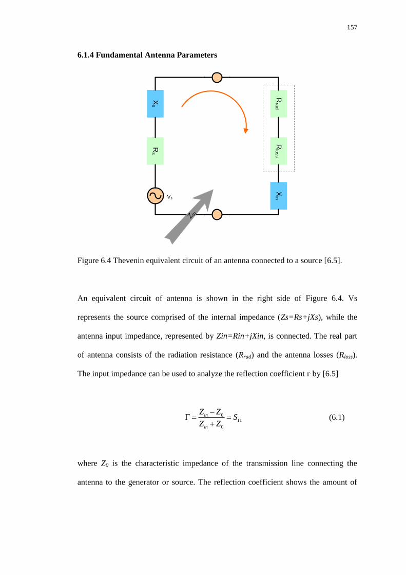
157
6.1.4 Fundamental Antenna Parameters
Vs
Xs
Rs
Rra
dR
loss
Xin
Z in
Figure 6.4 Thevenin equivalent circuit of an antenna connected to a source [6.5].
An equivalent circuit of antenna is shown in the right side of Figure 6.4. Vs
represents the source comprised of the internal impedance (Zs=Rs+jXs), while the
antenna input impedance, represented by Zin=Rin+jXin, is connected. The real part
of antenna consists of the radiation resistance (Rrad) and the antenna losses (Rloss).
The input impedance can be used to analyze the reflection coefficient г by [6.5]
011
0
in
in
Z ZS
Z Z
(6.1)
where Z0 is the characteristic impedance of the transmission line connecting the
antenna to the generator or source. The reflection coefficient shows the amount of

158
power reflected to the source. In ideal case, г should be zero. Therefore, the voltage
standing wave ratio is
1
1VSWR
(6.2)
The return loss is given by
20logRL (6.3)
Moreover, the input impedance is used to determine the antenna’s resonant
frequencies on Smith Chart with less reflection to the source by matching with the
feed line. In order to receive the maximum power transfer to antenna, the input
impedance, ideally, contains only a resistive real part which is the same value as the
internal resistance of the signal source.
6.1.5 Analysis of patch antenna
The basic formulation and relationship between dimensions of rectangular patch
antennas as well as the resonant frequency can be analyzed as follow [6.5]:
The substrate used for this case is RO3010 with a dielectric constant=10.2
and a height of 1.27mm.
The initial given values of the width (W) of the patch is calculated by using
the following formula. c is the speed of light in vacuum =3x10⁸m/s, fr is the
design resonant frequency.
0
0 0
1 2 2
1 2 12 r r rr
vW
ff
(6.4)
159
The effective dielectric constant of the conventional patch antenna is
calculated by
1/ 21 1
1 122 2
r rreff
h
W
(6.5)
Then, calculate the extended incremental length of the patch by
( 0.3) 0.264
0.412
( 0.258) 0.8
reff
reff
W
L h
Wh
h
(6.6)
The value of the effective length of the patch is calculated by
reff
efff
cL
02 (6.7)
The actual length of the patch is then provided by
2effL L L (6.8)
Finally, the resonant frequency is calculated by using the formula:
reff
rL
cf
2 (6.9)
6.2 CSRRs Properties and Antenna Design
The CSRRs loaded transmission line, and its equivalent circuit model, have been
proposed [6.12, 6.13], shown in Figure 6.5 (a) and (b). Figure 6.5 (a) represents the
topology of CSRRs which is composed of three parameters: air slot on ground plane

160
(d), its conductance (c), and the average ring dimension (r0), respectively. Owing to
the behavior of a CSRRs which acts as LC resonator, the equivalent circuit can be
modeled by Figure 6.5 (b). It can be seen that CSRRs are formed by the parallel
combination of Lr and Cr and its coupling to the host line, which are represented by
the capacitance Cc. The series gap on transmission line is represented by Cg
(a)
L/2 L/2
Lr
Cc
Cr
2Cg 2Cg
(b)
Figure 6.5 (a) The unit cell of CSRRs TL and (b) its T-equivalent circuit.
The intrinsic parallel resonant frequency (fc) of the CSRRs can be given by [6.12,
6.13].
To obtain fc, the shunt patch to the ground is opened. This gives directly the value of
L from the negative permittivity line. Then, the additional condition is,
Zs/2
Zp
d
c
r0

161
/ 2 / 2( ) ( )s pZ j Z j (6.10)
Zs and Zp are the series and shunt impedance of the T-equivalent circuit model of the
structure, respectively. Thus, the first factor to design is the radius of inner and outer
ring which mainly controls the resonant frequency of antenna. In this proposed
antenna, there is another factor which has been used to control the resonant
frequency. That is the meander line which will be explained in later.
6.2.1 Meander line antenna concept
Generally, a conventional microstrip patch antenna consists of a radiating patch
printed on one side of a dielectric substrate which has a ground plane on the other
side. The patch is normally made of conducting material such as copper. The
radiating patch and feed lines are usually etched on the dielectric substrate. In this
paper, the efforts on miniaturization were achieved mainly by focusing on etching
CSRRs on the ground plane with inductively meander line and capacitive gap on the
patch.
The idea of introducing a CSRRs particle on the ground plane of antenna structure is
to generate the negative permittivity at the design frequency which this coupling on
CSRRs is the first main key used to control the resonant frequency of antenna. Then,
the meandered line patch, acts as inductance, is applied for further controlling the
resonant frequency. The proposed rectangular microstrip patch antenna was designed

162
by using Ansoft HFSS simulation programme and validated experimentally using
Vector Network Analyzer (HP8510).
6.2.2 Design procedures
The antenna in this research was designed and adjusted to obtain a proper compact
dimension on Roger/RO3010 substrate and operates at 1.73GHz by Ansoft HFSS
simulation programme.
Figure 6.6 Antenna model by HFSS simulation programme
The antennas in three different meander line turns, as shown in Table 6.2, have been
studied and designed. The layout of the meander line and its geometrical parameters
are given in Figure 6.6 and 6.7. The introduced meander line with the capacitive gap,
acting as a series of inductors, by using the equation (6.10) to (6.12), helps to finely
match and tune the resonant frequency lower with maintain the patch size as
electrical small.
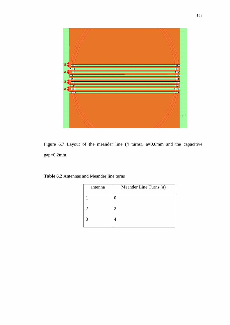
163
Figure 6.7 Layout of the meander line (4 turns), a=0.6mm and the capacitive
gap=0.2mm.
Table 6.2 Antennas and Meander line turns
antenna Meander Line Turns (a)
1 0
2 2
3 4
a
a
a
a

164
Figure 6.8 The simulated return loss (S11) of each CSRRs patch antenna.
The simulated antenna return losses are illustrated in Figure 6.8. The meander line
turns can move the resonant frequency lower and achieve better matching. However,
the CSRRs on the ground plane are a sensitive model, a few limited meander line
turn, as a fine tuning, can be accepted. The Bandwidth of antenna3 (dash blue line) is
narrow approximately 35MHz, reaching about 2% fractional bandwidth.
After applied the voltage source to antenna, the electric field has been generated as
well as fringing zone polarizing through the patch. Figure 6.9(a) and (b) show the
electric field distribution on the patch surface of the proposed antenna1 and antenna3
(x-y plane), respectively. Moreover, there is another electric field occurred by the
coupling between the inner and outer of the two rings of CSRRs which is opposite
direction to the original one. As a result, the electric field distributions on the
coupling area on patch have been created which provides a new resonant frequency.
The magnetic field distributions, illustrated by Figure 6.9(c) and (d), are
perpendicular to the electric field distribution.

165
(a) (b)
(c) (d)
Figure 6.9 The simulated field distributions at resonant frequencies (a) E field of
antenna1 at 1.8GHz and (b) E field of antenna3 at 1.73GHz, while (c) H field of
antenna1 at 1.8GHz and (d) H field of antenna3 at 1.73GHz, respectively.
Figure 6.10(a) and (b) demonstrate the surface’s current distributions cover all on
patch and ground of antenna3. At the resonate frequency of CSRRs, the current
direction was dominated by rearranging the direction on patch as well as happening
on ground. In addition, the inductive meander line on patch is also used to give better
coupling with CSRRs as tuning to get an optimum matching the antenna resonant
frequency.

166
(a)
(b)
Figure 6.10 The surface’s current distribution at 1.73GHz of antenna3 (a) on patch
(b) on ground, respectively.
6.2.3 Experimental results
The photos of the fabricated antenna are shown in Figure 6.11. The antenna was
fabricated on the RO3010 substrate, whose dielectric constant (εr) is 10.2, loss
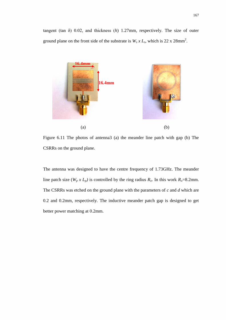
167
tangent (tan δ) 0.02, and thickness (h) 1.27mm, respectively. The size of outer
ground plane on the front side of the substrate is Ws x Ls, which is 22 x 28mm2.
(a) (b)
Figure 6.11 The photos of antenna3 (a) the meander line patch with gap (b) The
CSRRs on the ground plane.
The antenna was designed to have the centre frequency of 1.73GHz. The meander
line patch size (Wp x Lp) is controlled by the ring radius Ro. In this work Ro=8.2mm.
The CSRRs was etched on the ground plane with the parameters of c and d which are
0.2 and 0.2mm, respectively. The inductive meander patch gap is designed to get
better power matching at 0.2mm.
16.4mm
16.4mm

168
Figure 6.12 The return loss in dB by full wave HFSS simulation and VNA
measurement of meander line loaded patch antenna with CSRRs etched on the
ground.
Figure 6.12 shows the simulated and measured return losses for the proposed
antenna3 which has a meander line of 4 turns. It can be seen that the measured
results are well agreed with the simulated one. As mentioned in the previous section,
the size of this proposed CSRRs resonant antenna with meander line can be reduced
to reach the patch size of 0.095λ0 x 0.095λ0. This is much smaller compared to the
conventional patch antenna which has the patch size of 0.21λ0 x 0.16λ0. The size of
the proposed antenna can be reduced dramatically because the resonant frequency
can be controlled by the reaction of inner and outer coupling of the CSRRs instead of
the physical length of conventional patch. Moreover, with the help of meander line
and the capacitive cap, acting as inductive and capacitive loadings, the antenna can
reduce the size further.

169
6.3 A compact and tunable antenna
This section introduces a novel tunable compact antenna loaded with CSRRs. The
varactor diode (Infineon BB535) is used to tune the operation frequency. The
dimension of antenna is maintained the same as the previous section. The operation
frequency of a CSRRs loaded antenna without meander line as in the previous
section is 1.8GHz. The proposed varactor loaded CSRRs antenna can be tuned by
changing the DC bias.
Vs
Zso
urc
e
Zlo
ad
Varactor
Diode
DC bias
Figure 6.13 The simple structure of the proposed antenna with varactor diode.
Varactor diode can vary its inherit capacitance by reverse bias. The low reversed bias
voltage provides high inherit capacitance, while higher the reversed bias voltage will
decrease the diode capacitance, respectively. The equivalent circuit of the tunable
antenna is illustrated in Figure 6.13.

170
(a) (b)
Figure 6.14 The layout of tunable patch antenna (a) ground view and (b) patch view.
Figure 6.14(a) is the photograph of the varactor diode connecting on ground plane
via the second patch, whereas Figure 6.14(b) shows the patch view and the
connecting point of the varactor diode to the ground plane which is placed on the
second half of the patch in order to allow the constant electric wave pass through the
total patch size.
The bias can control the resonant frequency, shown in Figure 6.15. Without DC bias,
the antenna resonates at 1.15GHz with return loss of 33dB. After applied reversed
DC bias, the junction capacitance inside varactor diode decreases, resulting in
moving the resonate frequency higher. In the other words, the tunable antenna
provides the resonant frequency under the condition of the lower diode capacitance,
the higher resonant frequency. Moreover, in the frequency ranges of the working
antenna, the operated bandwidths are stable at 35MHz. After biasing DC to +12V,
there is no radiation from antenna (antenna is off) that because the completed

171
connecting of the depletion region inside diode presents a completed circuit loop and
is shorted to ground which is no diode capacitance at this frequency.
Figure 6.15 The measured return loss of the tunable CSRRs patch antenna with
different DC bias voltages.
As a result of diode applied CSRRs patch antenna, a fine tuning range is covered
350MHz from 1.15 to 1.5GHz with maintaining bandwidth at 35MHz. This is the
first shown the co-operation of CSRRs as mention before as well as the work of
diode application to fulfill the aim to minimize and tuning antenna.

172
6.4 Conclusion
Novel compact CSRRs loaded patch antennas with tunability have been studied,
designed, fabricated and characterized.
Microstrip patch antenna using CSRRs and capacitive loaded meander line can
reduce size by 74% in comparison with conventional rectangular patch antenna. The
size reduction was achieved by effectively manipulating the electromagnetic field
distributions within and between the meander line patch and CSRRs. More turns of
the meander line can move the operating frequency lower without changing any
dimension of patch which is maintained at 16.4x16.4mm2. In tunable antenna, the
size of antenna is still compact by keeping the previous dimension of without diode
case. The operation frequency of CSRRs antenna with diode is at 1.15GHz which is
lower than CSRRs antenna without diode at 1.8GHz in same dimension. After
applied DC voltage, the inherit capacitance of diode changes, leading to the change
of the overall impedances of the antenna. Therefore, the tunable CSRRs antenna can
be achieved. In this research, the operation frequency tunable range is 350MHz
cover the frequencies from 1.15 to 1.5GHz with stable 35MHz narrow bandwidth.

173
6.5 References
[6.1] J.B. Pendry, A.J. Holden, D.J. Robbins,”Magnetism from Conductors and
Enhanced Nonlinear Phenomena”, IEEE Trans. Microwave Theory and
Techniques, vol.47, no.11, p.2075-2084, 1999.
[6.2] D.R. Smith, W.J. Padilla,”Composite Medium with Simultaneously Negative
Permeability and Permittivity, Physical Review Lett., vol. 84, p. 4184-4187,
2000.
[6.3] D.-O. Kim, N.-I. Jo, D.-M. Choi, ”Design of The Ultra-Wideband Antenna
with 5.2 GHz/5.8 GHz Band Rejection using Rectangular Split-Ring
Resonators (SRRs) Loading”, J. of Electromagn. Waves and Appl., Vol. 23,
2503- 2512, 2009
[6.4] U. Lee and Y. Hao, ”Characterization of Microstrip Patch Antennas on
Metamaterial Substrates Loaded with Complementary Split-Ring
Resonators”, Microwave an Optical Technology Letters. Vol. 50, No.8,
August 2008
[6.5] C. A. Balanis, Antenna Theory: Analysis and Design, 3rd
ed. John
Wiley&Son, Inc, 2005. ISBN: 9780471714620
[6.6] W.L. Stutzman and G.A. Thiele, Antenna Theory and Design, 2nd
ed. New
York: Wiley, 1998.
[6.7] A. Kordzadeh and F. Hojat Kashani, “A New Reduced Size Microstrip Patch
Antenna with Fractal Shaped Defects,” Progress In Electromagnetic
Research B, Vol. 11, 29-37, 2009
[6.8] J. G. Joshi, S. S. Pattnaik, S. Devi, “Bandwidth Enhancement and Size
Reduction of Microstrip Patch Antenna by magneto inductive Waveguide
Loading”, Wireless Engineering and Technology, 2011, 2, 37-44
174
[6.9] H. F. Lee and W. Chen, Advances in Microstrip and Printed Antennas, John
Wiley&Son, Inc, 1997
[6.10] L. I. Basilio, J. T. Williams, D. R. Jackson, and M. A. Khayat, “A
Comparative study of a New GPS Reduced-Surface-Wave Antenna”, IEEE
Antenna and Wireless Propagation Letters, pp. 233-236, Vol.4, 2005
[6.11] W. G. Lim, H. S. Jang, and J. W. Yu, ”New Method for Back Lobe
Suppression of Microstrip Patch Antenna for GPS”, Proceeding of the 40th
European Microwave Conference, pp.679-682, 28-30 September 2010, Paris,
France
[6.12] J.D. Baena, J. Bonache, F. Martin, R. Marqués, F. Falcone, T. Lopetegi,
M.A.G. Laso, J. Garcia-Garcia, I. Gil, M. Flores, and M. Sorolla,”Equivalent
circuit models for split ring resonators and complementary split ring
resonators coupled to planar transmission lines”, IEEE Trans Microwave
Theory Tech 53 (2005), 1451-1461
[6.13] I. Gil, J. Bonache, M. Gil, J. Garcia-Garcia, and F. Martin,”Accurate circuit
analysis of resonant-type left handed transmission lines with inter-resonator
coupling”, Journal of Applied Physics 100, 074908 (2006).

175
CHAPTER 7
CONCLUSIONS AND FUTURE WORK
7.1 Conclusions
The aim of this research was to propose and examine a novel approach of CSRRs
and microstrip in communication components. In microstrip planar structure, the
left-handed band of the resonant-type metamaterial structure is formed by CSRRs
particle etched onto the ground plane. This CSRRs exhibit negative effective
permittivity, whereas the negative effective permeability can be obtained by etching
series gaps on the conductor strip, shown in Chapter 2.
The equivalent circuit and the left-handed area of CSRRs TL were analyzed in
Chapter 3. It was found that the magnetic coupling component should be added in
the lumped-element equivalent circuit model in the case of more than two adjacent
CSRRs cells. The analysis of the magnetic coupling effect was carried on by HFSS
full-wave electromagnetic simulation. The 2-unit cell of CSRRs TL was modeled
and placed. By varying the distance between these two CSRRs, the detected
magnetic couplings were captured and analyzed. The graph result of magnetic
coupling presented that there were some currents that appeared from 200A/m to
50A/m between 0.2mm to 1mm distances of these two rings, respectively. By using
ADS extracted the parameters of the 0.2mm distance case, the S11 graph of the
proposed equivalent circuit can present the resonant frequency (fc) at 2.27GHz
matching the S11 from full wave simulation, which was better than the old equivalent
circuit, which provides fc at 2.3GHz. The S11s on smith chart also agreed with the

176
new equivalent circuit. Another noticeable outcome in this chapter was the indicating
LH operating area of CSRRs TL. The 4-cell CSRRs TL was fabricated. It was
noticed that there were two passbands that appeared (≈2.2-2.5GHz and 4.7-6.5GHz).
The dispersion graph clearly indicated the left-handed area (<2.55GHz) and right-
hand area (>4.7GHz) of this fabricated 4-cell CSRRs TL. This left-handed area was
then further analyzed in chapter 4.
Because metamaterials present a specific dispersion property, under these dispersion
conditions, the first application in this thesis was to study the delay property in
CSRRs applied to microstrip TLs (chapter 4). Initially, the group delay relation of
both LH and RH areas were analyzed. It was found that in LH areas the group delay
is inversely proportional to frequency. Then, the group delays of these two cases
were investigated, which are passive delay line and active delay line. The group
delay of the previous 4-cell CSRRs TL of 35mm length was measured and referred
to passive delay line. The group delay graph results of both simulations and
measurement agreed with the previous analyzed theory, whereas in 35mm long
normal TL the group delay remained the same overall frequency at 0.3ns. In
comparison, at 2.3GHz the group delay of this 4-cell CSRRs TL displayed 3ns which
was 10 times that of a conventional TL. Then, the signal delays on a simple RF
system were examined. The two waveforms, CWs and pulses, were studied. By
loading the measured S-parameters to the data block in ADS, the three different
sinusoidal waves of 2.2, 2.3 and 2.4GHz were fed in the 4-cell CSRRs TL
simultaneously. The results showed that these three signals perform differently in
times, phases, and amplitudes at the port end, relating to the group delay graph.
Next, the two modulated different pulses with carrier 2.25 and 2.5GHz were fed in
177
simultaneously. At the output port, the delayed pulses consumed the time in CSRRs
TL at 6 and 5ns of the carrier wave at 2.25 and 2.5GHz, respectively. In active delay
line, the 4 diodes were embedded in the 4-cell CSRRs TL. Because of the change of
characteristic impedance resulting from diode addition, the operating frequency was
shifted. The group delays were detected by monitoring one frequency. For example,
after applied the DC bias to diodes from -10 to -20V, the group delay displayed the
tuning rate of 0.5ns/V at 2.03GHz.
Both simulation and measurement results in this chapter prove that the group delay
can be varied, and controlled, without changing the transmission line length, which
is not found in normal microstrip structure.
The later application was to develop a wideband passband filter, by using rectangular
CSRRs (chapter 5). The new filter configuration was achieved by the modified
structure of a narrow passband filter. A rectangular CSRRs was placed on ground
plane in the prototype model. The coupling between CSRRs and the coupling plate
of the host line generated a passband on the lower frequency side of the proposed
filter; as a result a high rejection in the lower band and the transmission zero were
presented. The novel filter exhibited a wide bandpass with a passband up to 77% of
the bandwidth covering the range from 0.9 to 1.9GHz. The insertion loss is less than
-1dB. Furthermore, the proposed filter presented the better performance in frequency
suppression on spurious frequency at 3.9GHz which appeared in the prototype filter.
The validated results were agreed through both equivalent circuit simulation and
measurement.

178
The last application is to minimize the size of planar antenna, which was done by
etching a CSRRs on the ground side of the patch antenna. A capacitive gap was also
etched on patch side. The originated frequency of the initial antenna was controlled
by the LC resonator of CSRRs, then it was applied the meander line part on the
middle of the patch to 2 and 4 turns. The simulated results showed that the operating
frequency was lower when applying more meander turns from 1.75GHz to 1.73GHz,
respectively. The measured S11 of the antenna with 4 turns of meander line agreed
with the HFSS full wave simulation. This novel planar antenna has shown 35MHz
bandwidth and significantly reduced the size to 74% of a conventional microstrip
patch antenna. In addition, inserting a diode from patch to ground can change the
proposed antenna to be active in selecting the operation frequency. After DC bias
was applied from 0V to 8V, the antenna provided the tuning range to 350MHz
covering the frequency 1.15GHz to 1.5GHz and maintaining its physical dimensions.
This proposed antenna maintained 35MHz bandwidth over all tuning ranges.
In summary, this thesis presents three areas of work, one showing that the
transmission line can control signal delay and reduce size, which means more data
can be multiplexed simultaneously. This thesis also shows the development of
enhanced bandwidth of a filter, from narrowband to wideband, by introducing only
the CSRRs particle. Finally the development of an antenna of a smaller size is also
demonstrated in this thesis. This thesis shows that introducing CSRRs in
RF/microwave components that can serve both miniaturization and performance
enhancement purposes.

179
7.2 Future works
This thesis provides the most fundamental part of communication systems. However,
there are some details that should be applied for more quality results. The future
works in this subject are provided in the list below;
In CSRRs applied microstrip transmission lines, the requirement of system
analysis is needed. This simple system is includes the signal and carrier
generator, mixer, and filter. Each part has to be placed on the same board.
Therefore, the more correct delay in the real system should be analyzed.
Because of the low gain appearance in electrically small antenna, in this
work, it is hard to get the radiation pattern. Placing the antenna in the form of
array antennas can support the gain enhancement. The further
implementation is very useful in analyzing the radiation.

180
LIST OF PUBLICATIONS
[1] S. Pasakawee and Z. Hu, “Compact Passive and Active Tunable Delay Lines
Using Complementary Split-Ring Resonators (CSRRs)”, Proceeding to IET
Microwaves, Antennas & Propagation. Manuscript ID: MAP-2012-0112.R1.
Accepted.
[2] S. Pasakawee and Z. Hu, “A Novel Wideband Filter Using Rectangular
CSRRs”, Advanced Electromagnetics Symposium (AES2012), April 16-19,
2012.
[3] S. Pasakawee and Z. Hu, “Electrical Small Meander Line Patch Antenna”, 6th
European Conference on Antennas and Propagation (EuCAP2012), March 26-
30, 2012.
[4] S. Pasakawee, M. A. Abdalla and Z. Hu , “"Microstrip Delay Line Implemented
by Complementary Split Ring Resonators (CSRRs)", 2nd International
Conference on Metamaterials, Photonic Crystals and Plasmonics (META
Conference, META'10), February 22-25, 2010.
[5] S. Pasakawee and Z. Hu, "Left-Handed Microstrip Delay Line Implemented by
Complementary Split Ring Resonators (CSRRs)", Asia Pacific Microwave
Conference (APMC 2009), December 7-10, 2009 P.60.
[6] S. Pasakawee and Z. Hu, "Left-handed Microstrip delay line implemented by
complementary split ring resonators", Loughborough Antennas & Propagation
Conference(LAPC 2009), Monday 16th November 2009.
[7] S. Pasakawee and Z. Hu, "The Delay Line of Left-Handed Microstrip
Implemented by Complementary Split Ring Resonators", the 2009
International Symposium on Antennas and Propagation (ISAP 2009), October
20-23, 2009.

181
Appendix
Figure 5.11 can be simplified as the equivalent circuits as follow:
L1 L12C1 2C1
C
Lr Cr
Cs CsL2
CM CM
The proposed filter is composed of network N1 and N2. N1 is in T-model, while N2
is in Pi-model, respectively.
L1 L12C1 2C1
C
Lr Cr
Z1 Z3
Z2
N1
Cs CsL2
CM CM
N2
Z5
Z4 Z6
The Z parameters of network N1 (T-model) are [5.1]

182
1 2 2
2 2 3
[ ]T
Z Z ZZ
Z Z Z
Then, convert the Z parameters to Y parameters by
2 311
1 2 1 3 2 3
T
Z ZY
Z Z Z Z Z Z
, 2
12
1 2 1 3 2 3
T
ZY
Z Z Z Z Z Z
221
1 2 1 3 2 3
T
ZY
Z Z Z Z Z Z
, 1 2
22
1 2 1 3 2 3
T
Z ZY
Z Z Z Z Z Z
The Z parameters of network N2 (Pi-model) are [5.1, 5.25, 5.26]
4 5 6 4 6
4 5 6 4 5 6
4 6 6 4 5
4 5 6 4 5 6
( )
( )
Z Z Z Z Z
Z Z Z Z Z ZZ
Z Z Z Z Z
Z Z Z Z Z Z
Change the Z parameter to Y parameters by
6 4 511
4 5 6
( )Z Z ZY
Z Z Z
, 12
5
1Y
Z
21
5
1Y
Z , 4 5 6
22
4 5 6
( )Z Z ZY
Z Z Z
N1 and N2 are in parallel connection. Therefore, the proposed filter can be derived in
Y parameters as
2 3 6 4 511
1 2 1 3 2 3 4 5 6
( )Z Z Z Z ZY
Z Z Z Z Z Z Z Z Z
212 21
1 2 1 3 2 3 5
1ZY Y
Z Z Z Z Z Z Z
4 5 61 222
1 2 1 3 2 3 4 5 6
( )Z Z ZZ ZY
Z Z Z Z Z Z Z Z Z