lesson9-rf oscillators
TRANSCRIPT

8/3/2019 lesson9-RF Oscillators
http://slidepdf.com/reader/full/lesson9-rf-oscillators 1/38
1
April 08 © 2006 by Fabian Kung Wai Lee 1
9 - RF Oscillator
The information in this work has been obtained from sources believed to be reliable.The author does not guarantee the accuracy or completeness of any informationpresented herein, and shall not be responsible for any errors, omissions or damagesas a result of the use of this information.
April 08 © 2006 by Fabian Kung Wai Lee 2
References
• [1]* D.M. Pozar, “Microwave engineering”, 2nd Edition, 1998 John-Wiley& Sons.
• [2] R. Ludwig, P. Bretchko, “RF circuit design - theory and applications”,2000 Prentice-Hall.
• [3] B. Razavi, “RF microelectronics”, 1998 Prentice-Hall, TK6560.
• [4] J. R. Smith,”Modern communication circuits”,1998 McGraw-Hill.
• [5] P. H. Young, “Electronics communication techniques”, 5th edition,2004 Prentice-Hall.
• [6] Gilmore R., Besser L.,”Practical RF circuit design for modern wirelesssystems”, Vol. 1 & 2, 2003, Artech House

8/3/2019 lesson9-RF Oscillators
http://slidepdf.com/reader/full/lesson9-rf-oscillators 2/38
2
April 08 © 2006 by Fabian Kung Wai Lee 3
Agenda
• Positive feedback oscillator concepts.
• Negative resistance oscillator concepts (typically employed for RFoscillator).
• Equivalence between positive feedback and negative resistanceoscillator theory.
• Oscillator start-up requirement and transient.
• Making an amplifier circuit unstable.
• Constant |Γ 1| circle.
• Fixed frequency oscillator design.
• Voltage-controlled oscillator design.
April 08 © 2006 by Fabian Kung Wai Lee 4
1.0 Oscillation Concepts

8/3/2019 lesson9-RF Oscillators
http://slidepdf.com/reader/full/lesson9-rf-oscillators 3/38
3
April 08 © 2006 by Fabian Kung Wai Lee 5
Classical Positive Feedback
Perspective on Oscillator (1)• Consider the classical feedback system with non-inverting amplifier:
• The system becomes unstable and oscillates when the following
condition occurs:
+
+
E(s) So(s)Si(s)
A(s)
F(s)
( )( )
( ) ( )sF s A
s A
iSoS s
−=
1
( ) ( ) ( )sF s AsT =PositiveFeedback Loop gain
( ) ( ) 01 =− sF s A
( ) ( ) 1>sF s A ( ) ( )( ) 0arg =sF s A
For sustained oscillation
For oscillation to startup
Barkhausen Criterion
Non-inverting amplifier
(1.1a)
(1.1b)
(1.2)
April 08 © 2006 by Fabian Kung Wai Lee 6
Classical Positive FeedbackPerspective on Oscillator (2)
• Possible feedback system can also be achieved with invertingamplifier:
+
-
E(s) So(s)Si(s)
-A(s)
F(s)
( )( )
( ) ( )sF s A
s A
iSoS s
−=
1
Inverting amplifier
Inversion

8/3/2019 lesson9-RF Oscillators
http://slidepdf.com/reader/full/lesson9-rf-oscillators 4/38
4
April 08 © 2006 by Fabian Kung Wai Lee 7
Example of Tuned Feedback Oscillator
(1)A 48 MHz Transistor Common-Emitter Colpitt Oscillator
0.2 0. 4 0. 6 0.8 1.0 1.2 1.4 1.6 1.80.0 2.0
-1.0
-0.5
0.0
0.5
1.0
1.5
-1.5
2.0
time, usec
V L ,
V
V B ,
V
+
-
E(s) So(s)Si(s)-A(s)
F(s)
VL
VB
VC
L
L1
R=
L=2.2 uH
V_DC
SRC1
Vdc=3.3 V
C
CD1
C=0.1 uF
C
Cc1
C=0.01 uF
C
Cc2
C=0.01 uF
C
CE
C=0.01 uF
C
C2
C=22.0 pF
C
C1
C=22.0 pF
R
RL
R=220 Ohmpb_mot_2N3904_19921211
Q1
R
RE
R=220 Ohm
R
RC
R=330 Ohm
R
RB2
R=10 kOhm
R
RB1
R=10 kOhm
April 08 © 2006 by Fabian Kung Wai Lee 8
Example of Tuned Feedback Oscillator(2)
A 27 MHz Transistor Common-BaseColpitt Oscilator
0.2 0.4 0. 6 0.8 1.0 1. 2 1.4 1.6 1. 80.0 2.0
-400
-200
0
200
400
-600
600
time, usec
V L , m V
V
E , m V
+
+
E(s) So(s)Si(s)
A(s)
F(s)
VL
VE
VB
VC
R
R1
R=1000 Ohm
C
C1
C=100.0 pF
C
C2
C=100.0 pF
L
L1
R=
L=1.0 uHC
C3
C=4.7 pF
R
RB2
R=4.7 kOhmR
RE
R=100 Ohm
R
RC
R=470 Ohm
V_DC
SRC1
Vdc=3.3 V
C
Cc1
C=0.1 uF
C
Cc2
C=0.1 uF
C
CD1
C=0.1 uF
pb_mot_2N3904_19921211
Q1
R
RB1
R=10 kOhm

8/3/2019 lesson9-RF Oscillators
http://slidepdf.com/reader/full/lesson9-rf-oscillators 5/38
5
April 08 © 2006 by Fabian Kung Wai Lee 9
Example of Tuned Feedback Oscillator
(3)
VLVC
VB
C
Cc2
C=0.1 uF
C
Cc1
C=0.1 uFC
CE
C=0.1 uF
sx_stk_CX-1HG-SM_A_19930601
XTL1
Fres=16 MHz
C
C2
C=22.0 pF
C
C1
C=22.0 pF
V_DC
SRC1
Vdc=3.3 V
C
CD1
C=0.1 uF
R
RL
R=220 Ohmpb_mot_2N3904_19921211
Q1
R
RE
R=220 Ohm
R
RC
R=330 Ohm
R
RB2
R=10 kOhm
R
RB1
R=10 kOhm
A 16 MHz Transistor Common-EmitterCrystal Oscillator
April 08 © 2006 by Fabian Kung Wai Lee 10
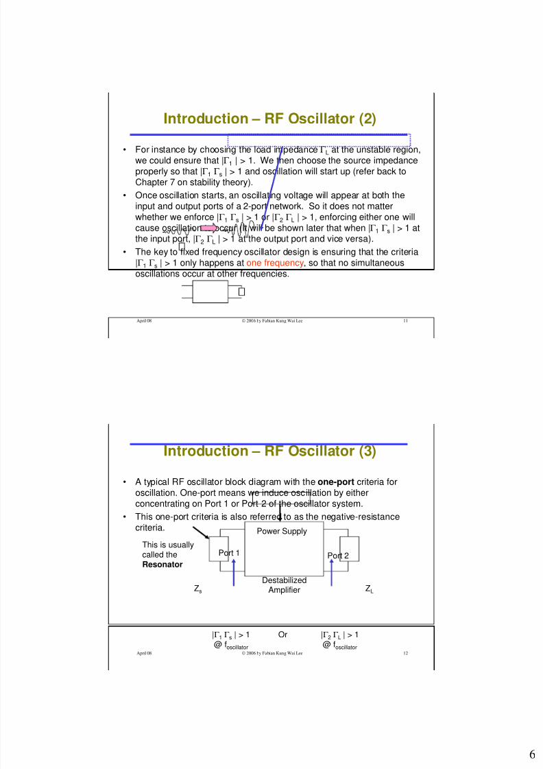
Introduction – RF Oscillator (1)
• In RF oscillator (foscillator > 300 MHz) , feedback method to induceoscillation can also employed. However it is difficult to distinguishbetween the amplifier and the feedback path, owing to the couplingbetween components and conductive structures on the printed circuitboard (PCB).
• An alternative perspective is to use the 1-port approach.• We can view an oscillator as an amplifier that produces an output
when there is no input,
• Thus it is an unstable amplifier that becomes an oscillator!
• The concept of stability analysis of small signal amplifier using stabilitycircles can be applied to RF oscillator design.
• Here instead of choosing load or source impedance in the stableregion of the Smith Chart, we purposely choose load or sourceimpedance in the unstable region. This will result in either |Γ 1 | > 1 or|Γ 2 | > 1 .
8/3/2019 lesson9-RF Oscillators
http://slidepdf.com/reader/full/lesson9-rf-oscillators 6/38
6
April 08 © 2006 by Fabian Kung Wai Lee 11
Introduction – RF Oscillator (2)
• For instance by choosing the load impedance Γ L at the unstable region,we could ensure that |Γ 1 | > 1. We then choose the source impedanceproperly so that |Γ 1 Γ s | > 1 and oscillation will start up (refer back toChapter 7 on stability theory).
• Once oscillation starts, an oscillating voltage will appear at both theinput and output ports of a 2-port network. So it does not matterwhether we enforce |Γ 1 Γ s | > 1 or |Γ 2 Γ L | > 1, enforcing either one willcause oscillation to occur (It will be shown later that when |Γ 1 Γ s | > 1 atthe input port, |Γ 2 Γ L | > 1 at the output port and vice versa).
• The key to fixed frequency oscillator design is ensuring that the criteria|Γ 1 Γ s | > 1 only happens at one frequency, so that no simultaneousoscillations occur at other frequencies.
April 08 © 2006 by Fabian Kung Wai Lee 12
Introduction – RF Oscillator (3)
• A typical RF oscillator block diagram with the one-port criteria foroscillation. One-port means we induce oscillation by eitherconcentrating on Port 1 or Port 2 of the oscillator system.
• This one-port criteria is also referred to as the negative-resistancecriteria. Power Supply
Zs ZL
DestabilizedAmplifier
|Γ 1 Γ s | > 1@ foscillator
|Γ 2 Γ L | > 1@ foscillator
Port 1 Port 2
Or
This is usuallycalled theResonator

8/3/2019 lesson9-RF Oscillators
http://slidepdf.com/reader/full/lesson9-rf-oscillators 7/38
7
April 08 © 2006 by Fabian Kung Wai Lee 13
Wave Propagation Stability Perspective (1)
• From our discussion of stability from wave propagation in Chapter 7…
Z1 or Γ 1
bs
bsΓ 1
bsΓ sΓ 1b
sΓ
sΓ
1
2
bsΓ s2Γ 1
2
bsΓ s2Γ 1
3
Source 2-portNetwork
Zs or Γ sPort 1 Port 2
s
s
sssss
ba
bbba
Γ Γ −=⇒
+Γ Γ +Γ Γ +=
11
22111
1
...
bsΓ s3Γ 1
3
bsΓ s3Γ 1
4
a1b1
Compare withequation (1.1a)
ssb
b
s
s
sssss
bb
bbbb
Γ Γ −
Γ =⇒
Γ Γ −
Γ =⇒
+Γ Γ +Γ Γ +Γ =
1
11
1
11
231
2111
1
1
...
( )( )
( ) ( )sF s A
s A
iSoS s
−=
1
Feedback is
provided by the
reflection due tosource mismatch
April 08 © 2006 by Fabian Kung Wai Lee 14
Wave Propagation Stability Perspective (2)
• Thus oscillation will occur when |Γ sΓ 1 | > 1.
• Similar argument can be applied to port 2, and we see that thecondition for oscillation is |Γ LΓ 2 | > 1.
• It is easier to work with impedance (admittance) in circuit design, sincethis can be related to lumped passive components.
• The following slides, with are adapted from Chapter 7, shows how theabove requirements can be cast into impedance form.

8/3/2019 lesson9-RF Oscillators
http://slidepdf.com/reader/full/lesson9-rf-oscillators 8/38
8
April 08 © 2006 by Fabian Kung Wai Lee 15
Source Network Port 1
Zs Z1
( ) ss
sss
V Z Z
Z V
X X j R R
jX RV
1
1
11
11
+=⋅
+++
+=
Oscillation Start-Up Requirements (1)
• We will derive the oscillation start-up requirement in terms of impedancefor Port. Assume Port 2 of the unstable amplifier is terminated with asuitable load impedance.
(1.3)
( )( ) sos
soss
jX Z R
jX Z R
++
+−=Γ
( )( ) 11
111
jX Z R
jX Z R
o
o
++
+−=Γ
Rs
jXs
R1
jX1
V ZL
Z2
Vamp
Port 2
April 08 © 2006 by Fabian Kung Wai Lee 16
Oscillation Start-Up Requirements (2)
From: ( )
( ) jX Z R
jX Z R
o
o
++
+−=Γ
( )
( )
( )
( )
( ) ( )( )
( ) ( )( )sosssosos
sosssosos
sos
sos
o
os
X X Z X R X R j X X Z R R Z R R
X X Z X R X R j X X Z R R Z R R
jX Z R
jX Z R
jX Z R
jX Z R
o
++++−+++
+−++−++−=
++
+−⋅
++
+−=Γ Γ
11112
11
11112
11
11
111 ω
( )( ) ( )( )
( )( ) ( )( )2111
2
12
11
2111
2
12
111
sosssosos
sosssososs
X X Z X R X R X X Z R R Z R R
X X Z X R X R X X Z R R Z R R
o
++++−+++
+−++−++−=Γ Γ
ω
Let ωo be the desired oscillation frequency
(1.4)
8/3/2019 lesson9-RF Oscillators
http://slidepdf.com/reader/full/lesson9-rf-oscillators 9/38
9
April 08 © 2006 by Fabian Kung Wai Lee 17
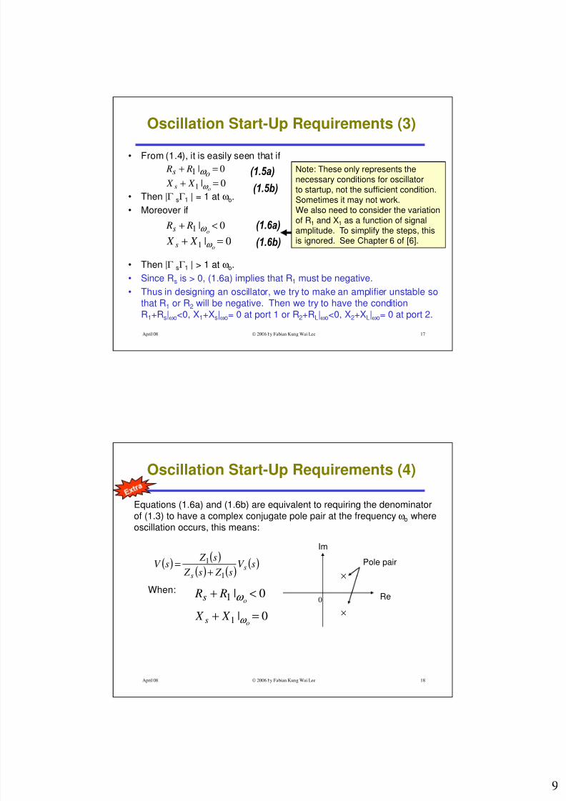
Oscillation Start-Up Requirements (3)
• From (1.4), it is easily seen that if
• Then |Γ sΓ 1 | = 1 at ωo.
• Moreover if
• Then |Γ sΓ 1 | > 1 at ωo.
• Since Rs is > 0, (1.6a) implies that R1 must be negative.• Thus in designing an oscillator, we try to make an amplifier unstable so
that R1 or R2 will be negative. Then we try to have the conditionR1+Rs|ωo<0, X1+Xs|ωo= 0 at port 1 or R2+RL|ωo<0, X2+XL|ωo= 0 at port 2.
0|1 =+os R R ω
0|1 =+o
X X s ω
(1.5a)
(1.5b)
0|1 <+o
R Rs ω
0|1 =+o
X X s ω
(1.6a)
(1.6b)
Note: These only represents thenecessary conditions for oscillatorto startup, not the sufficient condition.Sometimes it may not work.We also need to consider the variationof R1 and X1 as a function of signalamplitude. To simplify the steps, thisis ignored. See Chapter 6 of [6].
April 08 © 2006 by Fabian Kung Wai Lee 18
Oscillation Start-Up Requirements (4)
( ) ( )( ) ( ) ( )sV s Z s Z
s Z sV ss 1
1+
=
When: 0|1 <+o
R Rs ω
0|1 =+o
X X s ω
×
×
Re
Im
0
Equations (1.6a) and (1.6b) are equivalent to requiring the denominatorof (1.3) to have a complex conjugate pole pair at the frequency ωo whereoscillation occurs, this means:
Pole pair
8/3/2019 lesson9-RF Oscillators
http://slidepdf.com/reader/full/lesson9-rf-oscillators 10/38
10
April 08 © 2006 by Fabian Kung Wai Lee 19
What Happens During OscillationStart-Up?
• Usually the transient signal or noise signal from the environment willcontain a small component at the oscillation frequency. This forms the‘seed’ in which the oscillation built up.
• As the voltage amplitude in the two-port network increases, theassumption of small signal operation become invalid.
• For instance in BJT, nonlinear effects such as transistor saturation andcut-off will happen, this limits the beta of the transistor and finally limitsthe amplitude of the oscillating signal.
• Therefore, the design of oscillator in a nutshell is: Use linear analysis todesign an unstable system which would let any small transient signal tobuilt up gradually. As the transient signal increases, let the nonlinearity
of the circuit limits the final oscillation amplitude.
April 08 © 2006 by Fabian Kung Wai Lee 20
2.0 Fixed Frequency
Oscillator Design

8/3/2019 lesson9-RF Oscillators
http://slidepdf.com/reader/full/lesson9-rf-oscillators 11/38
11
April 08 © 2006 by Fabian Kung Wai Lee 21
Procedures of Designing Fixed
Frequency Oscillator (1)• Step 1 - Design a transistor/FET amplifier circuit.
• Step 2 - Make the circuit unstable by adding positive feedback at radiofrequency, for instance, adding series inductor at the base for common-base configuration.
• Step 3 - Determine the frequency of oscillation ωo and extract S-parameters at that frequency.
• Step 4 - With the aid of Smith Chart and Load Stability Circle, make R1
< 0 by selecting Γ L in the unstable region.
• Step 5 - Find Z1 = R1 + jX1.
April 08 © 2006 by Fabian Kung Wai Lee 22
Procedures of Designing FixedFrequency Oscillator (2)
• Step 6 - Find Rs and Xs so that R1 + Rs<0, X1 + Xs=0 (in order for | Γ 1Γ s |>1) at ωo. The rule of thumb is to make Rs=(1/3)|R1| .
• Step 7 - Design the impedance transformation network for Zs and ZL.
• Step 8 - Built the circuit or run a computer simulation to verify that thecircuit can indeed starts oscillating when power is connected.
• Note: Alternatively we may begin Step 4 using Source Stability Circleand work on | Γ 2 Γ L |> 1 at ωo .

8/3/2019 lesson9-RF Oscillators
http://slidepdf.com/reader/full/lesson9-rf-oscillators 12/38
12
April 08 © 2006 by Fabian Kung Wai Lee 23
Making an Amplifier Unstable (1)
• An amplifier can be made unstable by providing some kind offeedback.
• Two favorite transistor amplifier configurations used for oscillatordesign are the Common-Base configuration with Base feedback andCommon-Emitter configuration with Emitter degeneration.
April 08 © 2006 by Fabian Kung Wai Lee 24
Making an Amplifier Unstable (2)
Vout
Vin
L_StabCircleL_StabCircle1
LSC=l_stab_circle(S,51)
LStabCircle
S_StabCircle
S_StabCircle1SSC=s_stab_circle(S,51)
SStabCircle
StabFactStabFact1
K=stab_fact(S)
StabFact
RRe
R=100 Ohm
S_Param
SP1
Step=2.0 MHz
Stop=410.0 MHzStart=410.0 MHz
S-PARA METERS
DC
DC1
DC
CCLB
C=0.17 pF
C
CbC=10.0 nF
L
LB
R=L=22 nH
R
RLB
R=0.77 Ohm
C
Cc2C=10.0 nF
CCc1
C=10.0 nF TermTerm1
Z=50 Ohm
Num=1
LLC
R=
L=330.0 nH
LLE
R=
L=330.0 nH
V_DC
SRC1Vdc=4.5 V
TermTerm2
Z=50 OhmNum=2
RRb1R=10 kOhm
R
Rb2R=4.7 kOhm
pb_phl_BFR92A_19921214Q1
Positive feedbackhere
Common BaseConfiguration
This is a practical modelof an inductor
An inductor is addedin series with the bypasscapacitor on the baseterminal of the BJT.This is a form of positiveseries feedback.
Base bypasscapacitor
At 410MHz

8/3/2019 lesson9-RF Oscillators
http://slidepdf.com/reader/full/lesson9-rf-oscillators 13/38
13
April 08 © 2006 by Fabian Kung Wai Lee 25
Making an Amplifier Unstable (3)
freq410.0MHz
K-0.987
freq410.0MHz
S(1,1)1.118 / 165.6...
S(1,2)0.162 / 166.9...
S(2,1)2.068 / -12.723
S(2,2)1.154 / -3.535
Unstable Regions
s22 and s11 have magnitude > 1
Γ L PlaneΓ s Plane
April 08 © 2006 by Fabian Kung Wai Lee 26
Making an Amplifier Unstable (4)
Vout
pb_phl_BFR92A_19921214
Q1
C
Ce1
C=15.0 pF
C
Ce2
C=10.0 pF
R
Rb1
R=10 kOhm
R
Rb2
R=4.7 kOhm
Term
Term1
Z=50 Ohm
Num=1
C
Cc1
C=1.0 nF
R
Re
R=100 Ohm
C
Cc2
C=1.0 nF
L_StabCircle
L_StabCircle1
LSC=l_stab_circle(S,51)
LStabCircle
S_StabCircle
S_StabCircle1
SSC=s_stab_circle(S,51)
SStabCircle
StabFact
StabFact1K=stab_fact(S)
StabFact
S_Param
SP1
Step=2.0 MHz
Stop=410.0 MHz
Start=410.0 MHz
S-PARAMETERS
DC
DC1
DC
L
LC
R=
L=330.0 nH
V_DC
SRC1
Vdc=4.5 V
Term
Term2
Z=50 Ohm
Num=2
Positive feedback here
Common EmitterConfiguration
Feedback

8/3/2019 lesson9-RF Oscillators
http://slidepdf.com/reader/full/lesson9-rf-oscillators 14/38
14
April 08 © 2006 by Fabian Kung Wai Lee 27
Making an Amplifier Unstable (5)
freq410.0MHz
K-0.516
freq
410.0MHz
S(1,1)
3.067 / -47.641
S(1,2)
0.251 / 62.636
S(2,1)
6.149 / 176.803
S(2,2)
1.157 / -21.427
UnstableRegions
S22 and S11 have magnitude > 1
Γ L Plane Γ s Plane
April 08 © 2006 by Fabian Kung Wai Lee 28
Precautions
• The requirement Rs= (1/3)|R1| is a rule of thumb to provide the excessgain to start up oscillation.
• Rs that is too large (near |R1| ) runs the risk of oscillator fails to start updue to component characteristic deviation.
• While Rs that is too small (smaller than (1/3)|R1|) causes too much non-linearity in the circuit, this will result in large harmonic distortion of theoutput waveform.
V 2
Clipping, a sign oftoo much nonlinearity
t
Rs too small
t
V 2
Rs too large
For more discussion about the Rs = (1/3)|R1| rule,and on the sufficient condition for oscillation, see[6], which list further requirement.

8/3/2019 lesson9-RF Oscillators
http://slidepdf.com/reader/full/lesson9-rf-oscillators 15/38
15
April 08 © 2006 by Fabian Kung Wai Lee 29
Aid for Oscillator Design - Constant
|Γ ΓΓ Γ 1| Circle (1)• In choosing a suitable Γ L to make |Γ L | > 1, we would like to know the
range of Γ L that would result in a specific |Γ 1 |.
• It turns out that if we fix |Γ 1 |, the range of load reflection coefficient thatresult in this value falls on a circle in the Smith chart for Γ L .
• The radius and center of this circle can be derived from:
• Assuming ρ = |Γ 1 |:
L
L
S
DS
Γ −
Γ −=Γ
22
111
1
222
2211
**22
2
centerTS D
S DS
ρ
ρ
−+−=
222
22
2112Radius
S D
SS
ρ
ρ
−=
By fixing |Γ 1 | and changing Γ L .
(2.1a) (2.1b)
April 08 © 2006 by Fabian Kung Wai Lee 30
Aid for Oscillator Design - Constant|Γ ΓΓ Γ 1| Circle (2)
• The Constant |Γ 1 | Circle is extremely useful in helping us to choose asuitable load reflection coefficient. Usually we would choose Γ L thatwould result in |Γ 1 | = 1.5 or larger.
• Similarly Constant |Γ 2 | Circle can also be plotted for the sourcereflection coefficient. The expressions for center and radius is similar
to the case for Constant |Γ 1 | Circle except we interchange s11 and s22,Γ L and Γ s . See Ref [1] and [2] for details of derivation.

8/3/2019 lesson9-RF Oscillators
http://slidepdf.com/reader/full/lesson9-rf-oscillators 16/38
16
April 08 © 2006 by Fabian Kung Wai Lee 31
Example 2.1
• In this example, the design of a fixed frequency oscillator operating at410MHz will be demonstrated using BFR92A transistor in SOT23package. The transistor will be biased in Common-Base configuration.It is assumed that a 50Ω load will be connected to the output of theoscillator. The schematic of the basic amplifier circuit is as shown inthe following slide.
• The design is performed using Agilent’s ADS software, but the authorwould like to stress that virtually any RF CAD package is suitable forthis exercise.
April 08 © 2006 by Fabian Kung Wai Lee 32
Example 2.1 Cont...
• Step 1 - DC biasing circuit design and S-parameter extraction.
DC
DC1
DC
S_Param
SP1
Step=2.0 MHz
Stop=410.0 MHz
Start=410.0 MHz
S-PARAMETERS
StabFact
StabFact1
K=stab_f act(S)
StabFac t
L
LC
R=
L=330.0 nH
L
LE
R=
L=220.0 nH
L
LB
R=
L=12.0 nH
S_StabCircle
S_StabCircle1
source_stabcir=s_stab_circle(S,51)
SStabCircle
L_StabCircle
L_StabCircle1
load_stabcir=l_stab_circle(S,51)
LSt abCircle
Term
Term1
Z=50 OhmNum=1
C
Cc 1
C=1.0 nF
Term
Term2
Z=50 Ohm
Num=2
C
Cc 2
C=1.0 nF
R
Re
R=100 Ohm
C
C b
C=1.0 nF
V_DC
SRC1Vdc=4.5 V R
Rb1
R=10 kOhm
R
Rb2
R=4.7 kOhm
pb_phl_BFR 92A_19921214Q1
Port 1 - Input
Port 2 - Output
AmplifierPort 1 Port 2
L3 is chosen care-fully so that theunstable regionsin both Γ L and Γ splanes are largeenough.
8/3/2019 lesson9-RF Oscillators
http://slidepdf.com/reader/full/lesson9-rf-oscillators 17/38
17
April 08 © 2006 by Fabian Kung Wai Lee 33
Example 2.1 Cont...
freq410.0MHz
K-0.987
freq410.0MHz
S(1,1)1.118 / 165.6...
S(1,2)0.162 / 166.9...
S(2,1)2.068 / -12.723
S(2,2)1.154 / -3.535
Unstable Regions
Load impedance here will resultin |Γ 1| > 1
Source impedance here will resultin |Γ 2| > 1
April 08 © 2006 by Fabian Kung Wai Lee 34
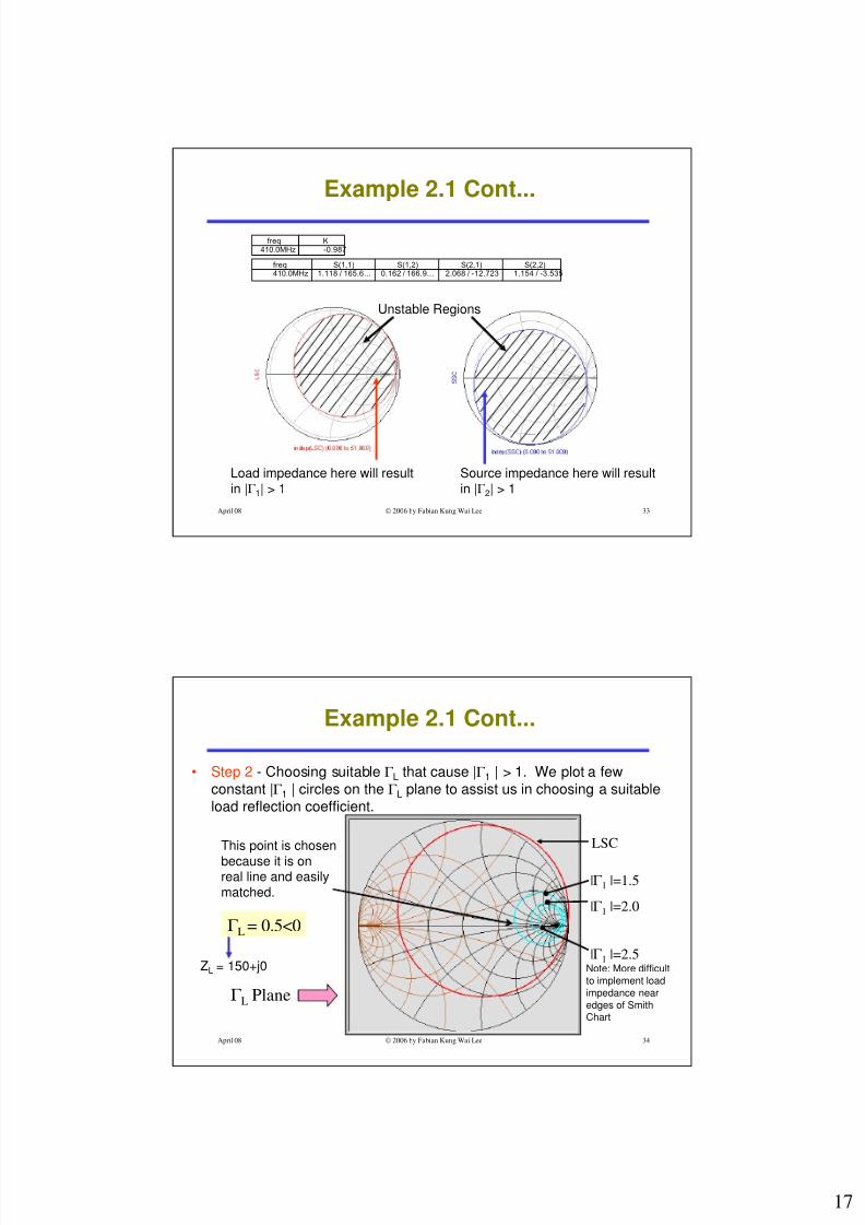
Example 2.1 Cont...
• Step 2 - Choosing suitable Γ L that cause |Γ 1 | > 1. We plot a fewconstant |Γ 1 | circles on the Γ L plane to assist us in choosing a suitableload reflection coefficient.
LSC
|Γ 1 |=1.5
|Γ 1 |=2.0
|Γ 1 |=2.5
Γ L = 0.5<0
This point is chosen
because it is onreal line and easilymatched.
Γ L Plane
Note: More difficult
to implement load
impedance near
edges of SmithChart
ZL = 150+j0

8/3/2019 lesson9-RF Oscillators
http://slidepdf.com/reader/full/lesson9-rf-oscillators 18/38
18
April 08 © 2006 by Fabian Kung Wai Lee 35
Example 2.1 Cont...
• Step 3 - Now we find the input impedance Z1 at 410MHz:
• Step 4 - Finding the suitable source impedance to fulfill R1 + Rs<0, X1
+ Xs=0:
851.7257.101
1
479.0422.11
1
11
22
111
j Z Z
jS
DS
o
L
L
+−=Γ −
Γ +=
+−=Γ −
Γ −=Γ
851.7
42.33
1
1
1
−≅−=
≅=
X X
R R
s
s
R1X1
April 08 © 2006 by Fabian Kung Wai Lee 36
Example 2.1 Cont...
Common-Base (CB)Amplifier
with feedback
Port 1 Port 2Zs = 3.42-j7.851
ZL = 150
• The system block diagram:

8/3/2019 lesson9-RF Oscillators
http://slidepdf.com/reader/full/lesson9-rf-oscillators 19/38
19
April 08 © 2006 by Fabian Kung Wai Lee 37
Example 2.1 Cont...
pF C
C
44.49851.7
1
1851.7
==
=
ω
ω
CB Amplifier3.42
27.27nH49.44pF
50
Zs= 3.42-j7.851 ZL=150
@ 410MHz3.49pF
• Step 5 - Realization of the source and load impedance at 410MHz.
April 08 © 2006 by Fabian Kung Wai Lee 38
Example 2.1 Cont... - Verification ThruSimulation
Vpp = 0.9VV = 0.45V
Power dissipated in the load:
mW
R
V P
L L
025.250
45.05.0
2
1
2
2
==
=
BFR92A
Vpp
8/3/2019 lesson9-RF Oscillators
http://slidepdf.com/reader/full/lesson9-rf-oscillators 20/38
20
April 08 © 2006 by Fabian Kung Wai Lee 39
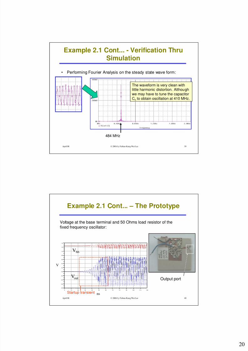
Example 2.1 Cont... - Verification Thru
Simulation• Performing Fourier Analysis on the steady state wave form:
484 MHz
The waveform is very clean withlittle harmonic distortion. Althoughwe may have to tune the capacitorCs to obtain oscillation at 410 MHz.
April 08 © 2006 by Fabian Kung Wai Lee 40
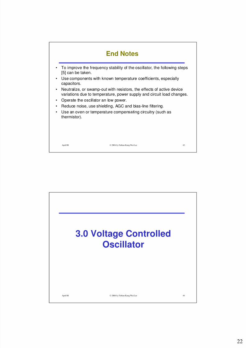
Example 2.1 Cont... – The Prototype
0 10 20 30 40 50 60 70 80 90 100 110 120
-0.8
-0.6
-0.4
-0.2
0.0
0.2
0.4
0.6
0.8
1.0
1.2
1.4
Voltage at the base terminal and 50 Ohms load resistor of thefixed frequency oscillator:
Output portVout
Vbb
V
nsStartup transient

8/3/2019 lesson9-RF Oscillators
http://slidepdf.com/reader/full/lesson9-rf-oscillators 21/38
21
April 08 © 2006 by Fabian Kung Wai Lee 41
Example 2.2 - Sample Oscillator
Design 2 Using Agilent’s ADS Software
R
RL
R=Rload
ParamSweep
Sweep1
Step=100
Stop=700
Start=100
SimInstanceName[6]=
SimInstanceName[5]=
SimInstanceName[4]=
SimInstanceName[3]=
SimInstanceName[2]=
SimInstanc eName[1] ="Tran1"
SweepVar="Rload"
PARAMET ER SWEEP
VAR
VAR1
Rload=100
X=1.0
EqnVar
Tran
Tran1
MaxTimeStep=1.2 nsec
StopTime=100.0 nsec
TRANSIENT
DC
DC 1
DC
C
Cb4
C=4.7 pF
V_DC
SRC1
Vdc=-1.5 V
C
Cb3
C=4.7 pF
di_sms_bas40_19930908
D1
L
L2
R=
L=47.0 nH
C
Cb2
C=10.0 pF
R
R1
R=4700 Ohm
C
Cb1
C=2.2 pF
R
Rb
R=47 kOhm
pb_phl_BFR92A_19921214
Q1
R
Re
R=220 Ohm
L
Lc
R=
L=220.0 nH
R
Rout
R=50 Ohm
CCc2
C=330.0 pF
V_DC
Vcc
Vdc=3.0 V
VtPWLVtrig
V_Tran=pwl(time, 0ns,0V, 1ns,0.01V, 2ns,0V)t
A UHF Voltage Controlled Oscillator:
April 08 © 2006 by Fabian Kung Wai Lee 42
Example 2.2 - Oscillator Start-upWaveform and Hardware 2
0 10 20 30 40 50 60 70 80 90 100
-1.5
-1.0
-0.5
0.0
0.5
1.0
Voltage across the load resistor RL:
Vout
ns
V
Output port
Auxiliarytriggersignal
Power splitter
8/3/2019 lesson9-RF Oscillators
http://slidepdf.com/reader/full/lesson9-rf-oscillators 22/38
22
April 08 © 2006 by Fabian Kung Wai Lee 43
End Notes
• To improve the frequency stability of the oscillator, the following steps[5] can be taken.
• Use components with known temperature coefficients, especiallycapacitors.
• Neutralize, or swamp-out with resistors, the effects of active devicevariations due to temperature, power supply and circuit load changes.
• Operate the oscillator an low power.
• Reduce noise, use shielding, AGC and bias-line filtering.
• Use an oven or temperature compensating circuitry (such asthermistor).
April 08 © 2006 by Fabian Kung Wai Lee 44
3.0 Voltage Controlled
Oscillator
8/3/2019 lesson9-RF Oscillators
http://slidepdf.com/reader/full/lesson9-rf-oscillators 23/38
23
April 08 © 2006 by Fabian Kung Wai Lee 45
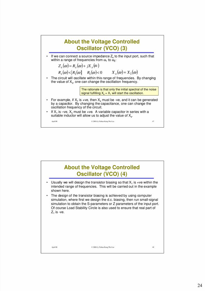
About the Voltage Controlled
Oscillator (VCO) (1)• A simple VCO using Clapp-Gouriet configuration.
• The transistor chosen for the job is BFR92A, a wide-band NPNtransistor which comes in SOT-23 package.
• Similar concepts as in the design of fixed frequency oscillator areemployed. Where we design the biasing of the transistor and carefullychoose a load so that from the input port (Port 1), the oscillator circuithas an impedance:
• Of which R1 is negative, for a range of frequencies from ω1 to ω2.
( ) ( ) ( )111 jX R Z +=
April 08 © 2006 by Fabian Kung Wai Lee 46
About the Voltage ControlledOscillator (VCO) (2)
Clapp-GourietOscillator Circuitwith Load
Zs
Z1 = R1 + jX1
ZL
8/3/2019 lesson9-RF Oscillators
http://slidepdf.com/reader/full/lesson9-rf-oscillators 24/38
24
April 08 © 2006 by Fabian Kung Wai Lee 47
About the Voltage Controlled
Oscillator (VCO) (3)• If we can connect a source impedance Zs to the input port, such that
within a range of frequencies from ω1 to ω2:
• The circuit will oscillate within this range of frequencies. By changingthe value of Xs, one can change the oscillation frequency.
• For example, if X1
is +ve, then Xs
must be -ve, and it can be generatedby a capacitor. By changing the capacitance, one can change theoscillation frequency of the circuit.
• If X1 is –ve, Xs must be +ve. A variable capacitor in series with asuitable inductor will allow us to adjust the value of Xs.
( ) ( ) ( )ω ω sss jX R Z +=
( ) ( ) ( ) 0 11 << ω ω ω R R Rs ( ) ( ) 1 ω ω X X s =
The rationale is that only the initial spectral of the noisesignal fulfilling Xs = X1 will start the oscillation.
April 08 © 2006 by Fabian Kung Wai Lee 48
About the Voltage ControlledOscillator (VCO) (4)
• Usually we will design the transistor biasing so that X1 is +ve within theintended range of frequencies. This will be carried out in the exampleshown here.
• The design of the transistor biasing is achieved by using computersimulation, where first we design the d.c. biasing, then run small-signal
simulation to obtain the S-parameters or Z parameters of the input port.Of course Load Stability Circle is also used to ensure that real part ofZ1 is -ve.

8/3/2019 lesson9-RF Oscillators
http://slidepdf.com/reader/full/lesson9-rf-oscillators 25/38
25
April 08 © 2006 by Fabian Kung Wai Lee 49
Schematic of the VCO
R
RL
R=Rload
ParamSweep
Sweep1
Step=100
Stop=700
Start=100
SimInstanceName[6]=
SimInstanceName[5]=
SimInstanceName[4]=
SimInstanceName[3]=
SimInstanceName[2]=
SimInstanceName[1]="Tran1"
SweepVar="Rlo ad"
PARAMET ER SWEEP
VAR
VAR1
Rload=100
X=1.0
EqnVar
Tran
Tran1
MaxTimeStep=1.2 nsec
StopTime=1 00.0 nsec
TRANSIENT
DCDC1
DC
C
Cb4
C=4.7 pF
V_DC
SRC1
Vdc=-1.5 V
C
Cb3
C=4.7 pF
di_sms_bas40_19930908
D1
L
L2
R=
L=47.0 nH
C
Cb2C=10.0 pF
R
R1R=4700 Ohm
C
Cb1
C=2.2 pF
R
Rb
R=47 kOhm
pb_phl_BFR92A_19921214
Q1
R
Re
R=220 Ohm
L
Lc
R=
L=220.0 nH
R
Rout
R=50 Ohm
C
Cc2
C=330.0 pF
V_DC
Vcc
Vdc=3.0 V
VtPWL
Vtrig
V_Tran=pwl(time, 0ns,0V, 1ns,0.01V, 2ns,0V)t
2-port network
Variablecapacitancetuning network
Initial noisesource to startthe oscillation
April 08 © 2006 by Fabian Kung Wai Lee 50
More on the Schematic
• L2 together with Cb3, Cb4 and the junction capacitance of D1 canproduce a range of reactance value, from -ve to +ve. Together thesecomponents form the frequency determining network.
• Cb4 is optional, it is used to limit the effect of the junction capacitanceof D1.
• R1 is used to isolate the control voltage Vdc from the frequencydetermining network. It must be a high quality SMD resistor. Theeffectiveness of isolation can be improved by adding a RF choke inseries with R1.
• Notice that the frequency determining network has no actualresistance to counter the effect of |R1(ω)|. This is provided by the lossresistance of L2 and the junction resistance of D1.

8/3/2019 lesson9-RF Oscillators
http://slidepdf.com/reader/full/lesson9-rf-oscillators 26/38
26
April 08 © 2006 by Fabian Kung Wai Lee 51
Time Domain Result
0 10 20 30 40 50 60 70 80 90 100
-1.5
-1.0
-0.5
0.0
0.5
1.0
Vout when Vdc = -1.5V
April 08 © 2006 by Fabian Kung Wai Lee 52
Load-Pull Experiment
100 200 300 400 500 600 700 800
1
2
3
4
5
• Peak-to-peak output voltage versus Rload for Vdc = -1.5V.
Vout(pp)
RLoad

8/3/2019 lesson9-RF Oscillators
http://slidepdf.com/reader/full/lesson9-rf-oscillators 27/38
27
April 08 © 2006 by Fabian Kung Wai Lee 53
Vout
Controlling Harmonic Distortion (1)
• Since the resistance in the frequency determining network is too small,large amount of non-linearity is needed to limit the output voltagewaveform, as shown below there is a lot of distortion.
April 08 © 2006 by Fabian Kung Wai Lee 54
Controlling Harmonic Distortion (2)
• The distortion generates substantial amount of higher harmonics.
• This can be reduced by decreasing the positive feedback, by adding asmall capacitance across the collector and base of transistor Q1. Thisis shown in the next slide.

8/3/2019 lesson9-RF Oscillators
http://slidepdf.com/reader/full/lesson9-rf-oscillators 28/38
28
April 08 © 2006 by Fabian Kung Wai Lee 55
Controlling Harmonic Distortion (3)
Capacitor to controlpositive feedback
CCcbC=1.0 pF
R
RLR=50 Ohm
RRoutR=50 Ohm
RReR=220 Ohm
LLc
R=L=220.0 nH
I_ProbeIC
pb_phl_BFR92A_19921214Q1
TranTran1
MaxTimeStep=1.2 nsecStopTime=280.0 nsec
TRANSIENT
DCDC1
DC
I_ProbeIload C
Cc2C=330.0 pF
LL2
R=L=47.0 nH
RRbR=47 kOhm
CCb1C=6.8 pF
CCb2C=10.0 pF
V_DCSRC1
Vdc=0.5 V
CCb4C=0.7 pF
CCb3C=4.7 pF
di_sms_bas40_19930908D1
RR1R=4700 Ohm
V_DCVccVdc=3.0 V
VtPWLVtrigV_Tran=pwl(time, 0ns, 0V, 1ns,0.01V, 2ns,0V)
t
The observantperson wouldprobably noticethat we can alsoreduce the harmonicdistortion by introducinga series resistance inthe tuning network.However this is notadvisable as the phasenoise at the oscillator’soutput will increase (more about this later).
April 08 © 2006 by Fabian Kung Wai Lee 56
Controlling Harmonic Distortion (4)
• The output waveform Vout after this modification is shown below:
Vout
8/3/2019 lesson9-RF Oscillators
http://slidepdf.com/reader/full/lesson9-rf-oscillators 29/38
29
April 08 © 2006 by Fabian Kung Wai Lee 57
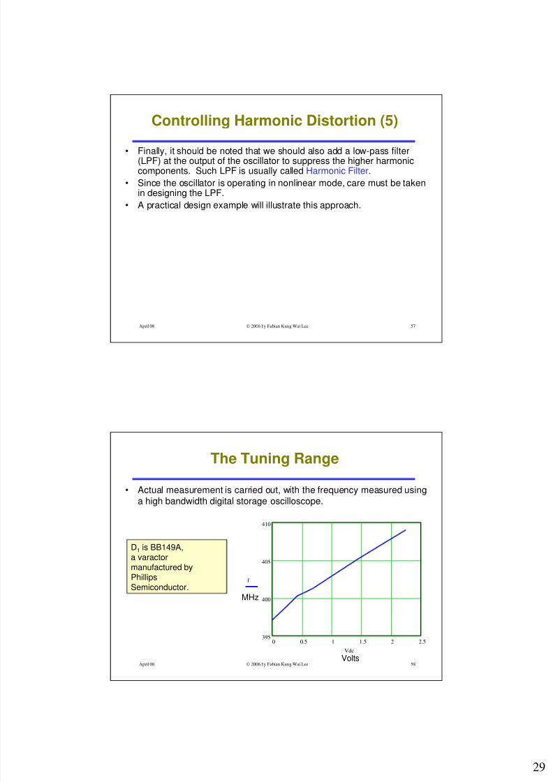
Controlling Harmonic Distortion (5)
• Finally, it should be noted that we should also add a low-pass filter(LPF) at the output of the oscillator to suppress the higher harmoniccomponents. Such LPF is usually called Harmonic Filter.
• Since the oscillator is operating in nonlinear mode, care must be takenin designing the LPF.
• A practical design example will illustrate this approach.
April 08 © 2006 by Fabian Kung Wai Lee 58
The Tuning Range
• Actual measurement is carried out, with the frequency measured usinga high bandwidth digital storage oscilloscope.
0 0.5 1 1.5 2 2.5395
400
405
410
f
Vdc
MHz
Volts
D1 is BB149A,a varactormanufactured byPhillipsSemiconductor.
8/3/2019 lesson9-RF Oscillators
http://slidepdf.com/reader/full/lesson9-rf-oscillators 30/38
30
April 08 © 2006 by Fabian Kung Wai Lee 59
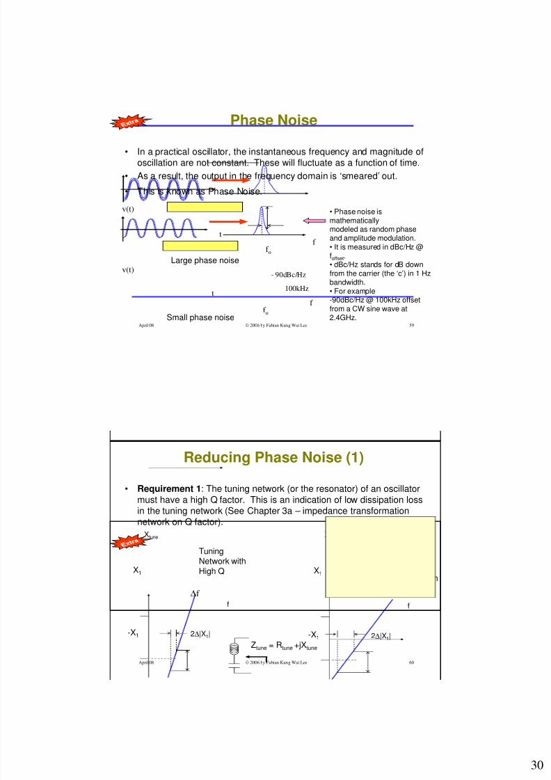
Phase Noise
• In a practical oscillator, the instantaneous frequency and magnitude ofoscillation are not constant. These will fluctuate as a function of time.
• As a result, the output in the frequency domain is ‘smeared’ out.
• This is known as Phase Noise.
t
v(t)
t
v(t)
f f o
f f o
- 90dBc/Hz
100kHz
Large phase noise
Small phase noise
• Phase noise ismathematicallymodeled as random phaseand amplitude modulation.• It is measured in dBc/Hz @foffset.• dBc/Hz stands for dB down
from the carrier (the ‘c’) in 1 Hzbandwidth.• For example-90dBc/Hz @ 100kHz offsetfrom a CW sine wave at2.4GHz.
April 08 © 2006 by Fabian Kung Wai Lee 60
Reducing Phase Noise (1)
• Requirement 1: The tuning network (or the resonator) of an oscillatormust have a high Q factor. This is an indication of low dissipation lossin the tuning network (See Chapter 3a – impedance transformationnetwork on Q factor).
X1
Xtune
-X1
∆f
f
2∆|X1|
TuningNetwork withHigh Q X1
Xtune
-X1
∆f
f
2∆|X1|
TuningNetwork withLow Q
Ztune = Rtune +jXtune

8/3/2019 lesson9-RF Oscillators
http://slidepdf.com/reader/full/lesson9-rf-oscillators 31/38
31
April 08 © 2006 by Fabian Kung Wai Lee 61
Reducing Phase Noise (2)
• A Q factor in the tuning network of at least 20 is needed for mediumperformance oscillator circuits at UHF. For highly stable oscillator, Qfactor of the tuning network must be in excess or 1000.
• We have looked at LC tuning networks, which can give Q factor of upto 40. Ceramic resonator can provide Q factor greater than 500, whilepiezoelectric crystal can provide Q factor > 10000.
• At microwave frequency, the LC tuning networks can be substitutedwith transmission line sections.
• See R. W. Rhea, “Oscillator design & computer simulation”, 2nd edition1995, McGraw-Hill, or the book by R.E. Collin for more discussions on
Q factor.• Requirement 2: The power supply to the oscillator circuit should also
be very stable to prevent unwanted amplitude modulation at theoscillator’s output.
April 08 © 2006 by Fabian Kung Wai Lee 62
More on Varactor
• The varactor diode is basically a PN junction optimized for its linear junction capacitance.
• It is always operated in the reverse-biased mode to preventnonlinearity, which generate harmonics.
• As we increase the biasing voltageVDC , C j decreases, hence theoscillation frequency increases.• The abrupt junction varactor has highQ, but low sensitivity (e.g. C j varieslittle over large voltage change).• The hyperabrupt junction varactorhas low Q, but higher sensitivity.
V j
V j0
C j
Linear region
Reverse biased
Forward biasedC jo
8/3/2019 lesson9-RF Oscillators
http://slidepdf.com/reader/full/lesson9-rf-oscillators 32/38
32
April 08 © 2006 by Fabian Kung Wai Lee 63
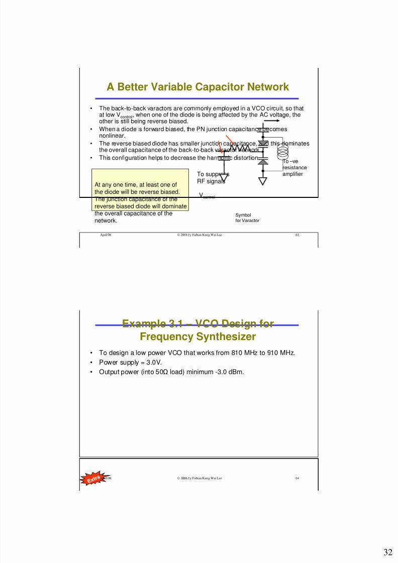
A Better Variable Capacitor Network
• The back-to-back varactors are commonly employed in a VCO circuit, so thatat low Vcontrol, when one of the diode is being affected by the AC voltage, theother is still being reverse biased.
• When a diode is forward biased, the PN junction capacitance becomesnonlinear.
• The reverse biased diode has smaller junction capacitance, and this dominatesthe overall capacitance of the back-to-back varactor network.
• This configuration helps to decrease the harmonic distortion.
At any one time, at least one ofthe diode will be reverse biased.
The junction capacitance of thereverse biased diode will dominatethe overall capacitance of thenetwork.
Vcontrol
Symbolfor Varactor
To suppressRF signals
To –veresistanceamplifier
April 08 © 2006 by Fabian Kung Wai Lee 64
Example 3.1 – VCO Design forFrequency Synthesizer
• To design a low power VCO that works from 810 MHz to 910 MHz.
• Power supply = 3.0V.
• Output power (into 50 load) minimum -3.0 dBm.

8/3/2019 lesson9-RF Oscillators
http://slidepdf.com/reader/full/lesson9-rf-oscillators 33/38
33
April 08 © 2006 by Fabian Kung Wai Lee 65
Example 3.1 Cont…
• Checking the d.c. biasing and AC simulation.
S_ParamSP1
Step=1.0 MHz
Stop=1.0 GHz
Start=0.7 GHz
S-PARAMETERS
DCDC1
DC
b82496c3120j000LCparam=SIMID 0603-C (12 nH +-5%)
4_7pF_NPO_0603
Cc1
100pF_NPO_0603
Cc2
2_2pF_NPO_0603C1
R
RER=100 Ohm
3_3pF_NPO_0603C2
RRL
R=100 Ohm
TermTerm1
Z=50 Ohm
Num=1
V_DC
SRC1Vdc=3.3 V
R
RBR=33 kOhm
pb_phl_BFR92A_19921214Q1
Z11
April 08 © 2006 by Fabian Kung Wai Lee 66
Example 3.1 Cont…
• Checking the results – real and imaginary portion of Z1 when output isterminated with ZL = 100.
m2freq=m2=-84.412
809.0MHzm1freq=m1=-89.579
775.0MHz
0.72 0.74 0.76 0.78 0.80 0.82 0.84 0.86 0.88 0.90 0.92 0.94 0.96 0.980.70 1.00
-110
-100
-90
-80
-70
-60
-50
-120
-40
freq, GHz
r e a l ( Z ( 1 , 1
) )
m2
i m a g ( Z ( 1 , 1
) )
m1

8/3/2019 lesson9-RF Oscillators
http://slidepdf.com/reader/full/lesson9-rf-oscillators 34/38
34
April 08 © 2006 by Fabian Kung Wai Lee 67
Example 3.1 Cont…
• The resonator design.
Vvar
VAR
VAR1
Vcontrol=0.2
EqnVar
C
C3
C=0.68 pF
L
L1
R=
L=10.0 nH
ParamSweep
Sweep1
Step=0.5
Stop=3
Start=0.0
SimInstanceName[6]=
SimInstanceName[5]=
SimInstanceName[4]=
SimInstanceName[3]=SimInstanceName[2]=
SimInstanceName[1]="SP1"
SweepVar="Vcontrol"
PARAMETER SWEEP
L
L2
R=L=33.0 nH
100pF_NPO_0603
C2
V_DC
SRC1
Vdc=Vcontrol V
S_Param
SP1
Step=1.0 MHz
Stop=1.0 GHz
Start=0.7 GHz
S-PARAMETERS
BB833_SOD323
D1
Term
Term1
Z=50 Ohm
Num=1
April 08 © 2006 by Fabian Kung Wai Lee 68
Example 3.1 Cont…
• The resonator reactance.
m1freq=m1=64.725Vcontrol=0.00000
882.0MHz
0.75 0.80 0.85 0.90 0.950.70 1.00
20
40
60
80
100
0
120
freq, GHz
i m a g ( Z ( 1 , 1
) )m1
- i m a g ( V C O_
a c . .
Z ( 1 , 1 ) )
Resonatorreactanceas a function ofcontrol voltage
The theoretical tuningrange
-X1 of the destabilized amplifier

8/3/2019 lesson9-RF Oscillators
http://slidepdf.com/reader/full/lesson9-rf-oscillators 35/38
35
April 08 © 2006 by Fabian Kung Wai Lee 69
Example 3.1 Cont…
• The complete schematic with the harmonic suppression filter.
Vvar
b82496c3120j000L3param=SIMID 0603-C (12 nH +-5%)
b82496c3100j000L1param=SIMID 0603-C (10 nH +-5%)
b82496c3330j000L2
param=SIMID 0603-C (33 nH +-5%)
RR1
R=100 Ohm
100pF_NPO_0603C4
b82496c3150j000L4param=SIMID 0603-C (15 nH +-5%)
0_47pF_NPO_0603C9
RRLR=100 Ohm2_7pF_NPO_0603
C8
100pF_NPO_0603Cc2
pb_phl_BFR92A_19921214Q1
TranTran1
MaxTimeStep=1.0 nsec
StopTime=1000.0 nsec
TRANSIENT
DCDC1
DC
CC7
C=3.3 pF
CC6C=2.2 pF
V_DC
SRC2Vdc=1.2 V
C
C5C=0.68 pF
BB833_SOD323D1
VtPWLSrc_trigger V_Tran=pwl(time, 0ns,0V, 1ns,0.1V, 2ns,0V)
t
4_7pF_NPO_0603Cc1
R
RER=100 Ohm
V_DCSRC1Vdc=3.3 V
R
RBR=33 kOhm
Low-pass filter
April 08 © 2006 by Fabian Kung Wai Lee 70
Example 3.1 Cont…
• The prototype and the result captured from a spectrum analyzer (9 kHzto 3 GHz).
VCOHarmonic
suppression filterFundamental-1.5 dBm
- 30 dBm

8/3/2019 lesson9-RF Oscillators
http://slidepdf.com/reader/full/lesson9-rf-oscillators 36/38
36
April 08 © 2006 by Fabian Kung Wai Lee 71
Example 3.1 Cont…
• Examining the phase noise of the oscillator (of course the accuracy islimited by the stability of the spectrum analyzer used).
300Hz
Span = 500 kHzRBW = 300 HzVBW = 300 Hz
-0.42 dBm
April 08 © 2006 by Fabian Kung Wai Lee 72
Example 3.1 Cont…
• VCO gain (ko) measurement setup:
SpectrumAnalyzer
Vvar
PortVout
Num=2
PortVcontrol
Num=1
RRcontrolR=1000Ohm
RRattnR=50Ohm
b82496c3120j000L3
param=SIMID 0603-C (12nH +-5%)
b82496c3100j000
L1param=SIMID 0603-C (10nH +-5%)
b82496c3150j000L4
param=SIMID 0603-C (15nH +-5%)
0_47pF_NPO_0603
C92_7pF_NPO_0603
C8
100pF_NPO_0603
Cc2
pb_phl_BFR92A_19921214
Q1
C
C7C=3.3pF
C
C6C=2.2pF
CC5
C=0.68pF
BB833_SOD323D1
4_7pF_NPO_0603
Cc1
RRER=100Ohm
V_DC
SRC1Vdc=3.3V
R
RBR=33 kOhm
Variable
powersupply
8/3/2019 lesson9-RF Oscillators
http://slidepdf.com/reader/full/lesson9-rf-oscillators 37/38
37
April 08 © 2006 by Fabian Kung Wai Lee 73
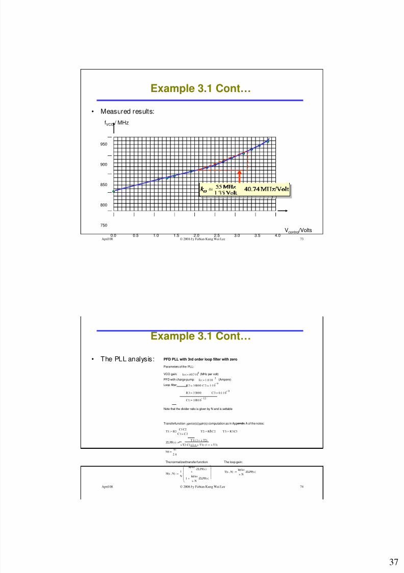
Example 3.1 Cont…
• Measured results:
0.0 0.5 1.0 1.5 2.0 2.5 3.0 3.5 4.0
750
800
850
900
950
fVCO / MHz
Vcontrol /Volts
April 08 © 2006 by Fabian Kung Wai Lee 74
Example 3.1 Cont…
• The PLL analysis:
H s N,( )1
N
k φ ko⋅
sZLPF s( )⋅
1k φ ko⋅
s N⋅ZLPF s( )⋅+
⋅:=T s N,( )
k φ ko⋅
s N⋅ZLPF s( )⋅:=
The loop gain:The normalized transfer function:
k φIo
2 π⋅:=
ZLPF s( )T 1 1 s T2⋅+( )⋅
s T2⋅ C1⋅ 1 s T1⋅+( )⋅ 1 s T3⋅+( )⋅:=
T3 R3C3⋅:=T2 R2 C2⋅:=T1 R2C1 C2⋅
C1 C2+⋅:=
Transfer function ∆θvco(s)/ ∆θin(s) computation as in Appendix A of the notes:
Note that the divider ratio is given by N and is settable
C1 10010
12−
⋅:=
C3 0.1 109−
⋅:=R3 33000:=
C2 1 109−
⋅:=R2 10000:=Loop filter:
(Ampere)Io 1.0 103−
⋅:=PFD with charge pump:
(MHz per volt)ko 40.7106
⋅:=VCO gain:
Parameters of the PLL:
PFD PLL with 3rd order loop filter with zero
8/3/2019 lesson9-RF Oscillators
http://slidepdf.com/reader/full/lesson9-rf-oscillators 38/38
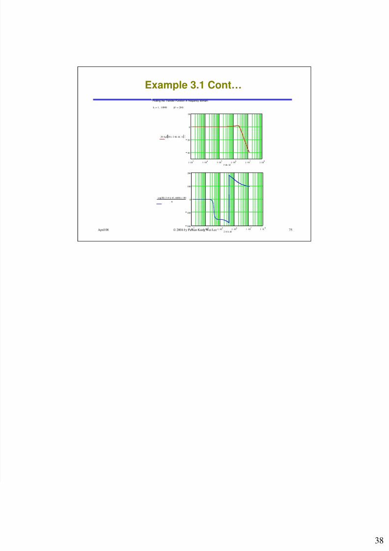
April 08 © 2006 by Fabian Kung Wai Lee 75
Example 3.1 Cont…
Plotting the Transfer Function in frequency domain:
k 1 10000..:= ∆f 20 0:=
1 .103
1 .104
1 .105
1 .106
1 .107
1 .108
40
20
0
20
20 log H i 2⋅ π⋅ k ∆f ⋅ 1,( )( )⋅
2 π⋅ k ∆f ⋅
1 .103
1 .104
1 .105
1 .106
1 .107
1 .108
200
100
0
100
200
arg H i 2⋅ π⋅ k ⋅ ∆f ⋅ 4400,( )( ) 180⋅
π
2 π⋅ k ⋅ ∆f ⋅