letter from the ceo 2 - maxim integrated - analog ... (in columns), hide and show columns, and...
TRANSCRIPT

Volume Sixty-Four
By simulating the behavior of a single Li+ cell under charge, this circuit lets you test Li+ battery chargers without using real batteries (see page 18).
MAX4163
1µFFILM
BATTERY VOLTAGESIGNAL OUTPUT
1V/V
DISCHARGE BATTERYINPUT SIGNAL
+5V0
1ms TO 10ms
BATTERY CURRENTSIGNAL OUTPUT
1V/A
DISCHARGE BATTERYPUSHBUTTONSPST, NO PB
0.22µF100kΩ
1%100kΩ
1%
10kΩ1%
10kΩ1%
10kΩ1%
121kΩ1%
100kΩ
SIGNAL COMMON
10kΩ
BATT+
BATT-
1kΩ
100mΩ5W
50kΩVAR
36kΩ
NDS0605
5.1kΩ 470Ω
10µF
1N4148
TIP32
TIP35
MAX8515
FB
PGND GND
IN OUT
61.9kΩ1%
A
B
LETTER FROM THE CEO 2
IN-DEPTH ARTICLES Unbalanced Twisted Pairs Can Give You the Jitters! 3
Negative Charge Pumps Achieve Inductor-Like Efficiency for WLED Backlights 13
Simplified Li+ Battery-Charger Testing 16

Letter from the CEOMaking Your Life Easier
For over 25 years, Maxim has been simplifying the lives of design engineers worldwide. Our highly integrated
engineering solutions reduce the complexity of designs, minimize system costs, and speed your time to market. And, with
over 5700 ICs in 28 product categories, we offer a broad range of solutions for your many design challenges.
Yet, we do more than provide integrated circuits. As fellow engineers, we also know that you have to make difficult
choices throughout the design process, and that time to market can frequently determine the success or failure of a design.
Thus, we have made it easier for you to find the right IC, evaluate potential solutions, and get technical support if you
encounter an obstacle in your design.
Maxim recently introduced a much-improved, web-based parametric search system to help you find exactly the right
part for your application. Designed by engineers for engineers, the revamped parametric tool offers the functionality you
need, while delivering extremely fast search responses.
For rapid navigation, all functions (such as searching and sorting) are executed locally by the user's browser. Thus,
once a product family page has loaded, there are no more calls back to Maxim’s server. Because it is so fast, the search
system can automatically update the list of matching products and the remaining available choices the instant you make a
selection. Additionally, the intelligent search algorithm only shows valid criteria, ensuring that you do not waste time
making selections that eliminate all products.
The parametric system also offers powerful filtering and sorting tools. You can sort hierarchically on any number of
parameters (in columns), hide and show columns, and select and compare any shortlist of products from the current results.
Again, all of this happens on your computer, so the search system is faster and more responsive than our competitors’ tools.
As ever, almost all of Maxim’s products are available as free samples upon request. To speed your evaluations, we
have increased the availability of samples and evaluation kits. We now ship over 55% of samples the same day, and over
95% the same week.
Should you encounter an obstacle in your design, Maxim’s dedicated technical support team is available to help you
find a solution. Internally, we have updated our request tracking system so that it monitors customer traffic on our website’s
Maxim Support Center. Requests are now entered into a database and tracked online, with replies and follow-ups threaded
and visible to our staff so that nothing falls through the proverbial cracks.
Whether through engineering solutions or up-to-date resources, Maxim continues to search for ways to make your
life easier. Stay tuned for simulation tools and more. And if there is anything else that we can do to better serve you, please
let me know at [email protected].
We are always at your service,
Tunç DolucaPresident and Chief Executive Officer
The Maxim logo is a registered trademark of Maxim Integrated Products, Inc. © 2008 Maxim Integrated Products, Inc. All rights reserved.

3
Unbalanced TwistedPairs Can Give Youthe Jitters! By Ron Olisar, Principal Member of Technical Staff
The transmission of serial-digital video above 1Gbps (asrequired by the DVI™, HDMI™, and DisplayPort™video-interface standards) has elevated the performancerequirements for the cables that connect PC and HDTVmonitors. Consequently, the traditional suppliers of analogaudio/video cable must now learn the same lessons thatmakers of datacom serial-digital differential cables learnedfor InfiniBand® and PCI Express® at 2.5Gbps, CX4 at3.125Gbps, and Fibre Channel at 4.25Gbps.
This article highlights the phenomenon of data jitter causedby conversions between differential- and common-modecomponents of the video signal. It also exposes mythsabout intrapair skew, and proposes cable tests for thepurpose of predicting jitter. The article demonstrates thatdifferential cables with good performance need not beexpensive, just well balanced.
The most common type of differential cable for digital-video signaling in the 0.25Gbps to 3.40Gbps range requiredby DVI/HDMI systems is 100Ω shielded twisted pair(STP). One-hundred-ohm twin-axial (twinax) cable is analternative, and is a mainstay of datacom applications.
Keeping Your BalanceDVI, HDMI, and DisplayPort systems each include fourlanes of differential interconnect for digital-video signaling.The signal can be recovered with inexpensive receiveelectronics, if two provisions are met: 1) the differentialpaths maintain the transmitted signals in differential mode,with little or no conversion to common mode; 2) thedifferential paths are balanced, which means that the twolines have symmetrical effects on the signal.
A cable that maintains signal energy in differential modeproduces predictable phase delays and skin-effect lossesacross the frequency spectrum. Both effects are easilycompensated. Otherwise, the signal may not be recoverableby an ordinary receiver. Indeed, conversion betweendifferential and common modes in a coupled differentialcable (STP or twinax) is an aberration that destroys theability to predict phase delay and signal loss.
A related measurement of signal corruption is intrapairskew, which results from different propagation delays onthe two lines of a differential pair. To illustrate, consider apair of twin-coax cables cut into different lengths (Figure1). The input is differential; that is, no common-modevoltage is present. The output, however, contains intrapairskew equal to the difference in propagation delays. Alongwith intrapair skew you find common-mode energy, as wellas reduced differential-mode energy.
The stimulus used in this example is sinusoidal, rather thana digital nonreturn-to-zero (NRZ) waveform. Skew delay
Figure 1. Simple intrapair skew converts some differential signal to common-mode (CM) energy.
CM
DIFF
Tx
Z
Z
+
-
+
-
DIFFERENTIAL INPUTOUTPUT WITH INTRAPAIR SKEW AND
COMMON-MODE ENERGY
TWIN COAX
SKEW
SKEW = ∆ DISTANCEPROPAGATION VELOCITY
CM
+
-
DIFF

4
for the simple twin-coax cable in Figure 1 is constant overfrequency. In STP or twinax cables, however, eachsinusoidal (Fourier) component of a digital NRZ waveformsuffers a different amount of skew.
Myths of Intrapair SkewA commonly measured symptom of conversion betweendifferential- and common-mode energy, intrapair skew isfrequently used by cable manufacturers as a QA test forcables. However, the conventional methods for measuringintrapair skew provide misleading results that are notpredictive of jitter.
Myth 1: Intrapair skew has a fixed value vs. frequency.
This statement is true for uncoupled differential pairs liketwin coax, but it is not true for coupled cables such as STPand twinax. Figure 2 illustrates this effect for 28AWGtwinax. Intrapair skew can actually reverse its polarity atdifferent frequencies.
Myth 2: Intrapair skew scales with cable length.
This characteristic is true at very low frequencies(wavelength long compared to the cable length), but it isnot true at high frequencies for coupled cables such as STPand twinax. Figure 2 shows the intrapair skew for variouslengths of 28AWG twinax. Note that between 300MHz and1500MHz, the 10-foot length has the worst intrapair skew.
Myth 3: Intrapair skew can be predicted using the step-stimulus test method.
This test launches a differential or single-ended voltage stepinto one end of a cable, and measures the time difference(skew) between (+) and (-) edges at the other end.Unfortunately, the cable itself lowpass-filters these outputedges, and that effect is dramatic in long cables. Thus, themethod demonstrates low-frequency intrapair skew, butsays nothing about the high-frequency intrapair skew thatmatters most for serial-digital video!
Again, intrapair skew is a function of frequency in STP andtwinax cables. Figure 3, for instance, shows measurementson a 50m 22AWG STP cable for DVI systems. Note thatthe step method predicts intrapair skew of 300ps, which isabout one half period (0.5UI) at the 1.65Gbps video ratenecessary for WUXGA displays. The cable, therefore, failsintrapair skew requirements for the DVI/HDMI standards.Yet, the receiver’s equalized eye diagram looks great,because the high-frequency intrapair skew is very low inthis cable, allowing excellent performance at 1.65Gbps.The step method only examines low-frequency intrapairskew. So, do not throw that cable away!
Figure 3. Step method fails to predict serial data jitter.
SKEW
(ps O
R m
UI)
FREQUENCY (MHz)
MAX3815 EQ OUTPUT 100ps/div
1000900800700600500400300200100
00 250 500 750 1000 1250 1500 1750 2000
1ns/div
OUTPUTS WITHDIFFERENTIAL STEP INPUT
SKEW (ps)SKEW (mUI)
INTRAPAIR SKEW vs. FREQUENCY
JITTER = 70ps210 - 1 PRBS AT1.65Gbps
NEGATIVE-POLARITY SIGNAL IS INVERTED FOR COMPARISON TOPOSITIVE-POLARITY SIGNAL. THEMEASUREMENT IS AT 50% LEVEL.
APPROX. 300ps50m, 22AWGDVI STP CABLE
Figure 2. Intrapair skew vs. frequency for 28AWG twinax.
FREQUENCY (MHz)
SKEW
(ps)
600
500
400
300
200
100
00 250 500 750 1000 1250 1500 1750 2000
90ft
50ft
30ft
10ft
INTRAPAIR SKEW (ps) FROM DC TO 2GHz

5
Coupled Differential PairsAs shown in Figure 4, coupled cables (STP, UTP, twinax)derive their differential characteristic impedance both fromcoupling between the (+) and (-) lines of a pair (Z1), andcoupling of each side to ground (Z2, Z3). Any imbalancein a differential pair, such as asymmetry of length, or twist,or dielectric environment (in which Z2 ≠ Z3), causes adifferential-to-common-mode conversion with measurablesymptoms, such as intrapair skew.
As a further complication in coupled cables, thedifferential- and common-mode signals have differentpropagation velocities, which can amount to severalnanoseconds of difference over the length of a long cable.As the differential energy converts to common-mode andback again, it returns with arbitrary phase. This effect isone source of differential-mode jitter. When the signal isable to convert freely between the two modes, the cablefrequency and phase responses are no longer predictable.
Differential- and common-mode signals also have differentloss rates (in dB/m) due to the skin effect. This behavior isnot all bad, because it can be used to advantage: a cablewhose common-mode loss is significantly higher than itsdifferential-mode loss has little intrapair skew. A cablewith no common-mode energy at the output end has nointrapair skew at all. As an extreme example, any high-frequency common-mode energy in a CAT5 UTP cabledissipates as EMI (because it has no shield), leaving onlydifferential-mode energy. Again, there is no intrapair skew.
Predicting Jitter from Differential-to-Common-Mode ConversionThe simple model of double conversion (differential modeto common mode and back) serves well here, though it isclearly a lumped approximation of a continuous process.Mode conversion is progressive and can be partial ormultigenerational, depending on the cable length relative towavelength (Figure 5).
Note that common-mode energy by itself does not imparttiming jitter to differential signaling. Rather, modeconversions corrupt the signal by permitting a return ofincoherent signals back into the differential mode. So, themeasurement of common-mode energy (given adifferential stimulus) provides evidence for modeconversion, from which we can then estimate thedifferential-mode jitter.
A measurement of cable quality should be predictive ofdigital-video signaling quality. For instance, it shouldpredict zero-crossing jitter in the data, which is the residualjitter that remains due to cable imbalances after an idealequalization of skin-effect and dielectric losses in thereceiver. Intrapair skew measurements using the stepstimulus are inadequate for predicting jitter.
We therefore propose the measurement of differential-to-common-mode conversion as a better predictor of data-jitter contribution from cable imbalance. Ideally, onlydifferential-mode, and not common-mode, energy remainsat the cable output. If common-mode energy is present, thecable has some imbalance and has converted somedifferential energy to common mode.
As a heuristic justification, we can use a simple model thathas a sine-wave differential source at the cable input.
1) Assume that a fraction of the sine-wave energy isconverted from differential to common mode in the cable,and by symmetry the same fraction is converted back todifferential mode. Using S-parameter naming conventions,the two conversion factors are SCD21 and SDC21,respectively (note that output ports are named first):
• SCD21 is differential-mode to common-modeconversion from Port 1 to Port 2
• SDC21 is common-mode to differential-modeconversion from Port 1 to Port 2
• SCD21(magnitude) = SDC21(magnitude) is a goodapproximation in real-world cables
• SDD21 is differential-mode transfer from Port 1 to Port 2
Figure 4. Uncoupled (twin coax) and coupled (twinax, STP) 100Ωdifferential pairs.
Z = 50Ω
+ + +
Z = 50Ω
-
100Ω TWIN COAX100Ω TWISTED-PAIR
OR TWINAX
Z1
Z2 Z3
Z1 (Z2 + Z3) = 100Ω
Figure 5. Illustration of mode conversion along cable length.
DIFFERENTIALSTIMULUS
DIFFERENTIAL-MODEOUTPUT
COMMON-MODEOUTPUT
MODE CONVERSION (IF ANY)
DIFFERENTIAL-MODE PROPAGATION VELOCITY
COMMON-MODE PROPAGATION VELOCITY

6
2) Assume that the energy making the full conversion(from differential to common mode and back) returns witharbitrary phase. This behavior results from differences inthe propagation velocity between differential and commonmodes, which is typical in STP and twinax. It also assumesa cable of sufficient length to exhibit a delay differencegreater than the sine period.
The zero crossing of a differential sinusoidal componentcan be shifted by TJ(pk), due to a returning version of itselfthrough SCD21 and SDC21 (Figure 6). Note the returneddifferential component, whose maximum amplitude at thezero crossing of the differential output signal causes theworst-case skew. The returned amplitude, A(dB), requiredto introduce TJ(pk) jitter relative to the total differentialoutput level (SDD21) is:
Eq. 1
A(dB) = [SCD21(dB) - SDD21(dB)] + [SDC21(dB)
- SDD21(dB)]
= 20 x LOGsin[2π x TJ(pk) x Frequency]
Because a good approximation for real-world cables isSCD21(magnitude) = SDC21(magnitude), the differencebetween common-mode and differential-mode levels at thecable output lets you measure the quality of a cable thatimparts less than TJ(pk-to-pk) jitter due to imbalance:
Eq. 2
SCD21(dB) - SDD21(dB) = A(dB)/2
< 10 x LOGsin[π x TJ(pk-to-pk) x Frequency]
Where added jitter due to imbalance is:
TJ(pk-to-pk) = 2 x TJ(pk)
Figure 7 shows the common- and differential-moderesponses of a cable, and Figure 8 plots their difference,showing common-mode relative to differential-modeoutputs. Figure 8 also includes templates for 0.1UI and0.2UI (lines of constant error in the differential zero-crossing TJ[pk]), where UI is the unit interval for the bitperiod at the given data rate. For example, the 0.1UI jitterline calculated for 1.65Gbps (WUXGA) represents aconstant maximum zero-crossing error of 60psP-P.
Template Interpretation and Simplification If the cable measurement in Figure 8 (SCD21 - SDD21)reaches the 0.1UI line at any point, cable imbalance createsa potential for 0.1UIP-P jitter. That is, if a spectralcomponent in the data-signaling sequence coincides with afrequency at which the cable measurement touches the0.1UIP-P template, the zero-crossing error (phase-shift range)for that spectral component is 0.1UIP-P (60psP-P).
DVI and HDMI TMDS® signaling is not scrambled, so theharmonic content of its frequency spectrum changesaccording to data content. It is, therefore, reasonable toassume that the entire spectrum will get “exercised” overtime, with dominant components falling roughly between(data rate)/20 and (data rate) x 0.8. (Note that the sinc2
power function of an NRZ data signal goes to zero atfrequency = data rate.)
Figure 6. Offset in the zero-crossing time TJ(pk) is caused by SCD21 and SDC21. All waveforms shown are differential signaling (single ended not shown).
1.0
0.8
0.6
0.4
0.2
-0.2
-0.4
-0.6
-0.8
-1.0
00 0.2 0.4 0.6 0.8 1.2 1.4 1.6 1.8 2
DIFFERENTIAL RETURNINGCOMPONENT THROUGH
SCD21 AND SDC21
DIFFERENTIAL OUTPUT
DIFFERENTIAL SOURCE
Tj(pk)
NORMALIZED UNIT INTERVAL
NORM
ALIZ
ED A
MPL
ITUD
E

7
Figure 7. Frequency response of a 60m cable, showing common-mode output (SCD21) and differential-mode output (SDD21). Data is gathered on the MAX3815 TMDS digital-video equalizer.
0
-10
-20
-30
-40
-50
-60
-70
FREQUENCY (MHz)
SKEW
(ps)
0 250 500 750 1000 15001250 1750 2000
AAATAAOUTPOUTPOUTPUT OF MAMMMMM X381XX 5 E55 QQQ
TESTSS PPPAAAPPPPP TTEREE N: PNNNN RBS RRAA 222 10 -1
THROUGH RESPONSE: SDD21 AND SCD21
SDD21
SCD21
Figure 8. Plot of (SCD21 – SDD21) difference, with pass/fail template superimposed.
0
-3
-6
-9
-12
-15
-18
-21
-24
-27
-30
SCD2
1 - S
DD21
(dB)
FREQUENCY (MHz)
0 250 500 750 1000 1250 1500 1750 2000
≥ FAIL 0.2UIP-P JITTERAT 1.65Gbps
≥ PASS 0.1UIP-P JITTERAT 1.65Gbps
SCD21 - SDD21
CRITERIA FOR 0.2UIP-P ADDEDJITTER AT 1.65Gbps DUE TO CABLEDIFF-TO-CM MEASURED FROM 5%TO 80% OF BIT RATE
CRITERIA FOR 0.1UIP-P ADDEDJITTER AT 1.65Gbps DUE TO CABLEDIFF-TO-CM MEASURED FROM 5%TO 80% OF BIT RATE
COMMON-MODE RELATIVE TO DIFFERENTIAL OUTPUT
8
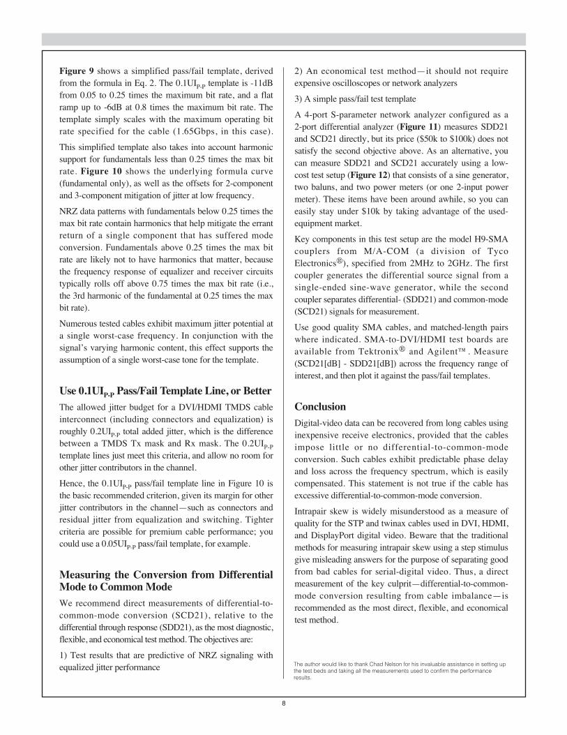
Figure 9 shows a simplified pass/fail template, derivedfrom the formula in Eq. 2. The 0.1UIP-P template is -11dBfrom 0.05 to 0.25 times the maximum bit rate, and a flatramp up to -6dB at 0.8 times the maximum bit rate. Thetemplate simply scales with the maximum operating bitrate specified for the cable (1.65Gbps, in this case).
This simplified template also takes into account harmonicsupport for fundamentals less than 0.25 times the max bitrate. Figure 10 shows the underlying formula curve(fundamental only), as well as the offsets for 2-componentand 3-component mitigation of jitter at low frequency.
NRZ data patterns with fundamentals below 0.25 times themax bit rate contain harmonics that help mitigate the errantreturn of a single component that has suffered modeconversion. Fundamentals above 0.25 times the max bitrate are likely not to have harmonics that matter, becausethe frequency response of equalizer and receiver circuitstypically rolls off above 0.75 times the max bit rate (i.e.,the 3rd harmonic of the fundamental at 0.25 times the maxbit rate).
Numerous tested cables exhibit maximum jitter potential ata single worst-case frequency. In conjunction with thesignal’s varying harmonic content, this effect supports theassumption of a single worst-case tone for the template.
Use 0.1UIP-P Pass/Fail Template Line, or BetterThe allowed jitter budget for a DVI/HDMI TMDS cableinterconnect (including connectors and equalization) isroughly 0.2UIP-P total added jitter, which is the differencebetween a TMDS Tx mask and Rx mask. The 0.2UIP-P
template lines just meet this criteria, and allow no room forother jitter contributors in the channel.
Hence, the 0.1UIP-P pass/fail template line in Figure 10 isthe basic recommended criterion, given its margin for otherjitter contributors in the channel—such as connectors andresidual jitter from equalization and switching. Tightercriteria are possible for premium cable performance; youcould use a 0.05UIP-P pass/fail template, for example.
Measuring the Conversion from DifferentialMode to Common ModeWe recommend direct measurements of differential-to-common-mode conversion (SCD21), relative to thedifferential through response (SDD21), as the most diagnostic,flexible, and economical test method. The objectives are:
1) Test results that are predictive of NRZ signaling withequalized jitter performance
2) An economical test method—it should not requireexpensive oscilloscopes or network analyzers
3) A simple pass/fail test template
A 4-port S-parameter network analyzer configured as a 2-port differential analyzer (Figure 11) measures SDD21and SCD21 directly, but its price ($50k to $100k) does notsatisfy the second objective above. As an alternative, youcan measure SDD21 and SCD21 accurately using a low-cost test setup (Figure 12) that consists of a sine generator,two baluns, and two power meters (or one 2-input powermeter). These items have been around awhile, so you caneasily stay under $10k by taking advantage of the used-equipment market.
Key components in this test setup are the model H9-SMAcouplers from M/A-COM (a division of TycoElectronics®), specified from 2MHz to 2GHz. The firstcoupler generates the differential source signal from asingle-ended sine-wave generator, while the secondcoupler separates differential- (SDD21) and common-mode(SCD21) signals for measurement.
Use good quality SMA cables, and matched-length pairswhere indicated. SMA-to-DVI/HDMI test boards areavailable from Tektronix® and Agilent™. Measure(SCD21[dB] - SDD21[dB]) across the frequency range ofinterest, and then plot it against the pass/fail templates.
ConclusionDigital-video data can be recovered from long cables usinginexpensive receive electronics, provided that the cablesimpose little or no differential-to-common-modeconversion. Such cables exhibit predictable phase delayand loss across the frequency spectrum, which is easilycompensated. This statement is not true if the cable hasexcessive differential-to-common-mode conversion.
Intrapair skew is widely misunderstood as a measure ofquality for the STP and twinax cables used in DVI, HDMI,and DisplayPort digital video. Beware that the traditionalmethods for measuring intrapair skew using a step stimulusgive misleading answers for the purpose of separating goodfrom bad cables for serial-digital video. Thus, a directmeasurement of the key culprit—differential-to-common-mode conversion resulting from cable imbalance—isrecommended as the most direct, flexible, and economicaltest method.
The author would like to thank Chad Nelson for his invaluable assistance in setting upthe test beds and taking all the measurements used to confirm the performanceresults.

9
Figure 9. Simplified test template, for which 0.1UIP-P pass/fail criteria are recommended.
0
200
300
400
500
600
700
800
900
1000
1100
1200
1300
1400
1500
160010
0
PASS
FAIL
0
-3
-6
-9
-12
-15
-18
-21
-8dB
-11dB
DIFF
-TO-
CM C
ONVE
RSIO
N (d
B)
= DI
FF-T
O-CM
(SCD
21) -
DIF
F-TO
-DIF
F (S
DD21
)
TEST FREQUENCY (MHz)
TEMPLATE FOR DIFF-TO-CM CONVERSION TEST
= 0.2UIP-P
= 0.1UIP-P
ADDITIVEDIFFERENTIALAT 1.65Gbps
82.5
MHz
= 0.
05 x
max
bit
rate
412M
Hz=
0.25
x m
ax b
it ra
te
1320
MHz
= 0.
80 x
max
bit
rate
TEST FREQUENCY (MHz)
200
300
400
500
600
700
800
900
1000
1100
1200
1300
1400
160010
0
PASS
= 0.2UIP-P
= 0.1UIP-P
0
-3
-6
-9
-12
-15
-18
-21
TEMPLATE FOR CABLE DIFF-TO-CM CONVERSION TEST
DIFF
-TO-
CM C
ONVE
RSIO
N (d
B)=
DIFF
-TO-
CM (S
CD21
) - D
IFF-
TO-D
IFF
(SDD
21)
0
1500
-8dB
-11dB
3-COMPONENT
FAIL
1237
MHz
= 0.
75 x
max
bit
rate
ADDITIVEDIFFERENTIAL JITTER
AT 1.65Gbps
FUNDAMENTALONLY
2-COMPONENT
82.5
MHz
= 0.
05 x
max
bit
rate
412M
Hz=
0.25
x m
ax b
it ra
te
825M
Hz=
0.5
x m
ax b
it ra
te
1320MHz= 0.80 x max bit rate
Figure 10. Simplified test template, with underlying family of curves shown for fundamental-only and multiple-harmonic cases.

10
Appendix: Real Cables Tell the Story
BALANCED 2-PORTS-PARAMETER
ANALYZER
MEASUREMENTS:
SDD21 =PORT 2 DIFFERENTIAL
RESPONSE RESULTING FROMPORT 1 DIFFERENTIAL STIMULUS
SCD21 =PORT 2 COMMON-MODERESPONSE RESULTING
FROM PORT 1 DIFFERENTIALSTIMULUS
PORT1
PORT2
MATCHED-PAIRSMA COAX CABLES:
PROP DELAYMISMATCH < 20ps
SMA-TO-DVI, ORSMA-TO-HDMITEST BOARDS
DVI OR HDMICABLE:
1 STP CHANNELUNDER TEST
+
-
+
-
MATCHED-PAIRSMA COAX CABLES:
PROP DELAYMISMATCH < 20ps
M/A-COM H-9HYBRID JUNCTION
COUPLER
SMACOAX
DIFFERENTIAL-MODE
LEVEL (DM)
COMMON-MODE
LEVEL (CM)
SMACOAX
SMA-TO-DVI, ORSMA-TO-HDMITEST BOARDS
DVI OR HDMICABLE:
1 STP CHANNELUNDER TEST
10MHz TO 2000MHzSINE-WAVEGENERATOR
2-CHANNEL RF POWER METER(MEASURES dB DIFFERENCE)
+
-
+
-
Figure 12. This test setup features a low-cost generator, couplers, andpower meters.
Figure 11. This 4-port S-parameter network analyzer is configured as a balanced 2-port analyzer.
FAIL
PASS
35m TWINAX28AWG, D0
SAMPLE: 1.65Gbps DVI35m 28AWG TWINAX CABLE
SKEW
(ps O
R m
UI)
S k e w ( p )
S k e w ( m U I)
EYE DIAGRAM AFTER MAX3815 RECEIVE EQ
1000
900
800
700
600
500
400
300
200
100
00 250 500 750 1000 1250 1500 1750 2000
INTRAPAIR SKEW FROM DC TO 2GHz
FREQUENCY (MHz)
SKEW (ps)
SKEW (mUI)
0
100
200
300
400
500
600
700
800
900
1000
1100
1200
1300
0
-3
-6
-9
-12
-15
-18
-21
> 0.2UIP-P ADDITIVE DIFFERENTIAL JITTER
< 0.1UIP-P ADDITIVE DIFFERENTIAL JITTER
TEST FREQUENCY (MHz)
DIFF
-TO-
CM C
ONVE
RSIO
N (d
B)=
DIFF
-TO-
CM (S
CD21
) - D
IFF-
TO-D
IFF
(SDD
21)
100ps/div
MAX3815 OUTPUT AT 1.65Gbps
JITTER = 45ps210 - 1 PRBSAT 1.65Gbps
165M
Hz=
0.1
x m
ax b
it ra
te
330
MHz
= 0.
2 x
max
bit
rate
660
MHz
= 0.
4 x
max
bit
rate
990
MHz
= 0.
6 x
max
bit
rate
12.5
MHz
= 0
.05
x m
in b
it ra
te
82.
5MHz
= 0
.05
x m
ax b
it ra
te

11
SAMPLE: 1.65Gbps DVI50m 22AWG STP CABLE
EYE DIAGRAM AFTER MAX3815 RECEIVE EQ
0
100
200
300
400
500
600
700
800
900
1000
1100
1200
1300
0
-3
-6
-9
-12
-15
-18
-21
> 0.2UIP-PADDITIVE DIFFERENTIAL JITTER
FAIL
PASS
< 0.1UIP-PADDITIVE DIFFERENTIAL JITTER
TEST FREQUENCY (MHz)SK
EW IN
(ps O
R m
UI)
1000
900
800
700
600
500
400
300
200
100
00 250 500 750 1000 1250 1500 1750 2000
INTRAPAIR SKEW FROM DC TO 2GHz
FREQUENCY (MHz)
SKEW (ps)
SKEW (mUI)
DIFF
-TO-
CM C
ONVE
RSIO
N (d
B)=
DIFF
-TO-
CM (S
CD21
) - D
IFF-
TO-D
IFF
(SDD
21)
MAX3815 OUTPUT AT 1.65Gbps
100ps/div
JITTER = 70ps210 - 1 PRBSAT 1.65Gbps
50m STP22AWG, D2
12.5
MHz
= 0
.05
x m
in b
it ra
te
82.
5MHz
= 0
.05
x m
ax b
it ra
te
165M
Hz=
0.1
x m
ax b
it ra
te
330
MHz
= 0.
2 x
max
bit
rate
660
MHz
= 0.
4 x
max
bit
rate
990
MHz
= 0.
6 x
max
bit
rate
132
0MHz
= 0.
8 x
max
bit
rate
1400 1500 1600
SAMPLE: 1.65Gbps DVI35m 22AWG STP CABLE
EYE DIAGRAM AFTER MAX3815 RECEIVE EQ
TEST FREQUENCY (MHz)
INTRAPAIR SKEW FROM DC TO 2GHz
FREQUENCY (MHz)
SKEW
IN (p
s OR
mUI
)
1000
900
800
700
600
500
400
300
200
100
00 250 500 750 1000 1250 1500 1750 2000
SKEW (ps)
SKEW (mUI)
0
100
200
300
400
500
600
700
800
900
1000
1100
1200
1300
0
-3
-6
-9
-12
-15
-18
-21
DIFF
-TO-
CM C
ONVE
RSIO
N (d
B)
= DI
FF-T
O-CM
(SCD
21) -
DIF
F-TO
-DIF
F (S
DD21
)
JITTER = 190ps210 - 1 PRBSAT 1.65Gbps
100ps/div
MAX3815 OUTPUT AT 1.65Gbps
> 0.2UIP-PADDITIVE DIFFERENTIAL JITTER
< 0.1UIP-PADDITIVE DIFFERENTIAL
JITTER
990
MHz
= 0.
6 x
max
bit
rate
132
0MHz
= 0.
8 x
max
bit
rate
165M
Hz=
0.1
x m
ax b
it ra
te
330
MHz
= 0.
2 x
max
bit
rate
660
MHz
= 0.
4 x
max
bit
rate
12.5
MHz
= 0
.05
x m
in b
it ra
te
82.
5MHz
= 0
.05
x m
ax b
it ra
te
35m STP22AWG, D2
FAIL
PASS

High-Frequency Losses in Long CablesSkin-effect and dielectric loss are the dominant high-frequency loss mechanisms in a cable. Fortunately,commercial DVI/HDMI equalizer ICs (such as theMAX3815) are available to extend cable reach byeconomically compensating these losses.
Skin-effect loss (in dB) is proportional to cable length andto the square root of frequency. Dielectric loss (in dB) isproportional to cable length and frequency. Skin-effect lossdominates from low to mid frequencies, and dielectric lossdominates at high frequencies.
Such losses introduce jitter due to ISI (inter-symbolinterference). An uncompensated loss of 6dB to 8dB at halfthe bit rate increases jitter, and lowers amplitude, to fullclosure of the eye diagram displayed on an oscilloscope. Bycompensating these losses, economical equalization canremove the ISI-related jitter and restore signal amplitude.
M/A-COM H9-SMA Hybrid Junction CouplerFrequency Range: 2MHz to 2000MHz
Impedance: 50Ω
Transmission Through-Loss: 3.4dB to 4.8dB (see graphbelow)
Mode Isolation: 30dB (min, see graph below)
Application 1: Single-ended-to-differential converter
Port A: Single-ended stimulus input
Port B: Connect 50Ω termination
Port C: Differential (+) output
Port D: Differential (-) output
Application 2: Mode splitter (separate differential andcommon modes)
Port C: Differential (+) input
Port D: Differential (-) input
Port A: Differential level output (single ended)
Port B: Common-mode level output (single ended)
The plot below shows Application 2, with the outputs ofports A and B in response to inputs at ports C and D. Theupper line (port A) is the differential stimulus at ports C andD, and the lower line (port B) is the common-modestimulus at ports C and D.
A B
C
D
0º
HYBRIDMAGIC
TEE
0º
0º180º
12
0
-10
-20
-30
-40
-50
-60
-70
FREQUENCY (Hz)
THRO
UGH
RESP
ONSE
(dB)
0 5.00E+08 1.00E+09 1.50E+09 2.00E+09
M/A-COM H9 COUPLER RESPONSEAT OUTPUT PORT A FROMCOMMON-MODE STIMULUSINTO PORTS C AND D
M/A-COM H9 COUPLER RESPONSEAT OUTPUT PORT A FROM DIFFERENTIAL-MODE STIMULUS INTO PORTS C AND D
Agilent is a trademark of Agilent Technologies, Inc.DisplayPort is a trademark of Video Electronics Standards Association (VESA).DVI is a trademark of Digital Display Working Group (DDWG).HDMI is a trademark of HDMI Licensing, LLC.InfiniBand is a registered trademark of System I/O, Inc., DBA InfiniBand TradeAssociation.PCI Express is a registered trademark of PCI-SIG Corp.Tektronix is a registered trademark of Tektronix, Inc.TMDS is a registered trademark of Silicon Image, Inc.Tyco Electronics is a registered trademark of Tyco International Services, GmbH.

Negative ChargePumps AchieveInductor-LikeEfficiency forWLED BacklightsBy Jay Kim, Senior Scientist
Offering a small footprint and high light output, whiteLEDs (WLEDs) provide an ideal backlight solution forsmall color displays in cellular phones and other portabledevices. WLEDs, however, do present one difficulty indevices powered from a single-cell lithium-ion (Li+)battery. The operating voltage from most Li+ cells is 3V to4.2V, while a WLED’s forward voltage is typically 3.5V to3.8V (at 20mA). Consequently, the voltage output at thelower end of a Li+ battery’s operating range is not enoughto bias WLEDs.
Two approaches are commonly used to generate adequateforward bias for WLEDs: capacitor-charge-pump andinductor-based boost circuits. Inductor-based circuits aregenerally the best choice for efficiency and battery life.However, they require the addition of that costly inductor,and necessitate careful layout and design to avoidelectromagnetic and radio-frequency interference issues. Incontrast, charge-pump solutions are simpler to implementand cost less, but they have also typically been lessefficient, which can reduce battery runtime.
With the advent of negative-charge-pump designs, newWLED driver ICs achieve inductor-like efficiencies(averaging 85%) while still retaining the simplicity and lowcost of an inductorless design.
Efficiency Improvements Among Fractional-Ratio Charge PumpsThe first generation of WLED charge-pump solutions useda basic doubler topology (or 2x mode) at its core. Theefficiency of a 2x charge pump is:
PLED/PIN = (VLED x ILED)/[(2 x VIN x ILED) + (IQ x VIN)]
Where IQ is the circuit’s quiescent operating current.
Because the IQ is usually small when compared to theWLEDs’ load current, the efficiency can be closelyapproximated by:
PLED/PIN ≈ VLED/(2VIN)
To improve efficiency, second-generation WLED chargepumps did not always drive the output to a whole multipleof the input. If the battery voltage was sufficient, anadequate WLED drive voltage could be generated with a1.5x charge pump. The conversion efficiency of a 1.5xpump is:
PLED/PIN = (VLED x ILED)/[(1.5 x VIN x ILED) + (IQ x VIN)]
≈ VLED/(1.5VIN)
As can be seen, the 1.5x pump substantially improvesefficiency. With a 3.6V battery voltage and a 3.7V WLED,efficiency jumps from 51% with a 2x pump to 69% with a1.5x pump.
Third-generation WLED drivers maximize efficiency evenmore. They employ a 1x transfer mode to connect thebattery directly to the WLEDs through low-dropout currentregulators when the battery voltage is high enough to drivethe WLEDs. The efficiency of a 1x transfer mode is:
PLED/PIN = (VLED x ILED)/[(VIN x ILED) + (IQ x VIN)]
≈ VLED/(VIN)
When the battery voltage is sufficient to directly driveWLEDs, 1x mode efficiency can be over 90%. With a 4Vbattery and a 3.7V WLED, efficiency is 92%.
Maximizing Efficiency at Each Battery VoltageAn optimum WLED driver design employs the mostefficient power-transfer mode possible for a given batteryand LED voltage. The design also changes modes as thebattery (or WLED) voltage changes. However, switchlosses can force the circuit into a less efficient mode at ahigher battery voltage than might otherwise be necessary. Itis always best for the driver to stay in a high-efficiencymode as long as possible while the battery voltage falls.However, this performance requires minimum loss in thepower switches and, consequently, more space and cost.
As noted above, the best conversion efficiency is offered bya 1x transfer mode, but this mode can only be used whenthe battery voltage is more than the WLEDs’ forwardvoltage (VF). The key to utilizing 1x mode for the lowestpossible battery voltage has usually focused on loweringboth the voltage drop of the 1x mode bypass FET and thatof the current regulator. These voltage drops determine theseries losses and minimum input voltage that can sustain 1xmode. The minimum battery voltage required by 1x mode is:
VIN(MIN_1x) = (VLED + Bypass pFET RDS(ON)) x (ILED
+ VDROPOUT of the current regulator)
A traditional positive-charge-pump WLED solution uses apFET bypass switch to connect the battery voltage to the
13

WLEDs, as shown in Figure 1. This FET’s RDS(ON) istypically 1Ω to 2Ω. Further resistance reductions arelimited since lower resistances typically would necessitatea larger FET, increasing the cost of the power device.
A positive charge pump generates 1.5x VIN or 2x VIN todrive the WLED anodes when VIN is insufficient to drive a1x transfer mode. To implement the 1x mode in a positive-charge-pump architecture, we must use an additionalinternal switch to route VIN directly to the WLEDs’ anodes,thereby bypassing the charge pump.
A negative-charge-pump architecture also generates -0.5xVIN to drive WLED cathodes when VIN is insufficient forthe task. This architecture, however, does not require thatyou bypass the -0.5x VIN charge-pump output to ground in1x mode because current regulators control the WLEDs’current directly from VIN to ground. As a result, thenegative-charge-pump architecture extends 1x mode all theway down to:
VIN(MIN_1x) = VLED + VDROPOUT of the current regulator
Figure 2 shows the current path of 1x mode with anegative charge pump. The circuit does not require apMOS bypass switch, and it directly regulates WLEDcurrent from VIN to ground. If ILED is 100mA total (i.e., 5WLEDs x 20mA), a 2Ω pMOS bypass switch’s voltagedrop would be 200mV. As it discharges, the Li+ batteryvoltage holds relatively stable around the 3.6V to 3.8V(typical) voltage range. Assuming a typical Li+ battery-discharge curve, the 200mV increase in operating voltageenabled by 1x mode dramatically improves efficiency.
Maximizing Efficiency at Each LED ForwardVoltageIn a traditional 1x/1.5x positive-charge-pump WLEDdriver, the WLED anodes connect to the charge pump’soutput. If the WLEDs are mismatched, the driver mustswitch to 1.5x mode when there is not enough (VIN - VLED)headroom to support the worst forward-voltage WLED.
With the negative-charge-pump architecture, it is no longernecessary to abandon the efficient 1x mode due to the badforward voltage of only one WLED. As Figure 2illustrates, the Mode Mux circuit individually selects 1xmode or -0.5x mode for each WLED, thereby maximizingoverall efficiency.
The MAX8647/MAX8648 charge-pump drivers, forexample, turn on the -0.5x charge pump when the inputvoltage is insufficient to drive the highest forward-voltageWLED. In this situation, the devices drive only the highestVF WLED through the -0.5x negative rail (instead ofground), while the WLEDs with lower forward voltagesremain in 1x mode.
To further improve efficiency, the MAX8647/MAX8648provide individual mode switching for the WLEDs. Thistechnology adaptively switches the WLEDs to -0.5x modeat different times and at different VIN levels due to VF
mismatches or temperature changes (Figure 3).
14
1.5x POSITIVECHARGE PUMP
CONTROLCIRCUITRY
CURRENT-SINK
REGULATORS
LED1
VDROPOUT
LED2
LED3
LED4
ENLEDON/OFFAND
DIMMINGCONTROL
IN
1.5x1x
C+CIN
C- C+Li+
BATTERYPOS
GND
CPOS
CF CF
RDS(ON)
C-
Figure 1. In 1x mode, the positive charge pump uses an internal switch to bypass VIN to the WLEDs’ anodes.
Figure 2. Individual switchover for each WLED is possible when the driver switches to its negative-charge-pump mode, which improves overall efficiency.
C+ C- C+ C-
Li+BATTERY
CNEG
NEG
CF CF
CONTROLCIRCUITRY
-0.5x NEGATIVECHARGE PUMP
CURRENT-SINK
REGULATORS
LED1
LED2
LED3
LED4
MODE MUX
ENLEDON/OFFAND
DIMMINGCONTROL
IN
IN
1x-0.5x
CIN
GND

15
SummaryTraditionally, WLED backlight designs that employ chargepumps have been less efficient than inductor-based designs.A positive-charge-pump architecture switches from itshighest efficiency mode (1x) when any single WLEDcurrent falls below a predetermined level. Thus, systemswith a large number of WLEDs and large forward-voltagemismatch waste a significant amount of power.
A negative-charge-pump architecture overcomes theinefficiencies typically encountered in positive-charge-pump designs. Devices such as the MAX8647/MAX8648use this negative-charge-pump architecture, as well asindividual mode switching for each LED, to dramaticallyimprove efficiency and extend battery runtime. TheseWLED drivers enable designers to achieve inductor-likeefficiencies while benefiting from the simplicity and costsavings offered by charge-pump solutions.
EFFICIENCY vs. INPUT VOLTAGE
INPUT VOLTAGE TIMEWEIGHTED (V)
100
MAX8648 VF LED = 3.2V TO 3.45V
1x/1.5x POSITIVE-CHARGE-PUMP VF LED = 3.2V TO 3.45V
EFFICIENCY GAINED BYNEGATIVE-CHARGE-PUMP
TECHNOLOGY
80
90
70
EFFI
CIEN
CY (%
)
60
50
404.20 3.89 3.81 3.75 3.69 3.63 3.56 3.50 3.32
EFFICIENCY GAINED BYINDIVIDUAL MODE
SWITCHING
Figure 3. The efficiency of the MAX8647/MAX8648 charge-pump WLED drivers can be extended by switching to a negative-charge-pump mode and to individual mode switching for each WLED.

Simplified Li+Battery-ChargerTesting By Alfredo H. Saab, Applications Engineering Manager,and Shasta Thomas, Applications Engineer
Lithium-ion (Li+) batteries are more delicate than otherbattery chemistries and have little tolerance for abuse.Consequently, Li+ battery chargers are complex circuits,requiring highly accurate current and voltage settings. Ifthese accuracy requirements are not met, the charger mayfail to completely charge the battery, severely reducebattery life, or otherwise degrade battery performance.
Given the demands imposed on Li+ chargers, it is criticalthat charger designs be tested thoroughly and steppedthrough their entire operating range. However, testing a Li+charger with its natural load (i.e., a Li+ battery) can be timeconsuming and impractical in laboratory and productionenvironments. To simplify the process, this article presentsa battery-emulation circuit for accelerated, realistic testingof Li+ battery chargers without actual batteries.
CC-CV ChargingThe Li+ battery-charging process requires medium-accuracy constant-current (CC) charging in a first phase,transitioning to high-accuracy constant-voltage (CV)charging in a second phase.
Figure 1 illustrates the V-I characteristics of a modernCC-CV integrated circuit (the MAX1737) used for a Li+battery charger. This type of IC is at the heart of all Li+
battery chargers in consumer products. The CC (between2.6V and 4.2V battery voltage) and the CV (4.2V) regionsare clearly shown.
The region below 2.6V requires a different chargingtechnique. If charging is attempted on a battery dischargedbelow 2.6V, the charger applies a low-value (“conditioningcurrent”) charging current until the battery reaches the 2.6Vlevel. This is a safety mechanism made necessary by thebehavior of Li+ batteries when overdischarged. Forcing afast-charge current when VBATT < 2.6V can cause thebattery to go into an irreversible short-circuit condition.
The transition point from the CC to the CV phase has acritical tolerance of ±40mV. The reason for the narrowtolerance is that a lower CV will not allow the battery toacquire its full charge, and a higher one will reduce itsuseful life.
Charge-process termination involves sensing that thebattery has reached its full charge and that the charger mustbe disconnected or shut down. This is accomplished bydetecting, while in the CV phase, the point where thecharge current is reduced to a fraction (usually < 10%) ofthe so-called fast-charge or maximum charge current.
Testing Parameters for Li+ ChargersLi+ battery-charger designs usually have two basic buildingblocks: a digital block (control state machine) and ananalog block, composed of a well-regulated current/voltagepower supply with an accurate (better than 1%) reference.A complete test of a Li+ charger product (not just the IC) isa more involved and time-consuming task than justverifying a few current or voltage values.
Testing should step the charger through its entire operatingrange: through the CC phase, up to the transition from CCto CV, and on to charge termination. Recall that the mostrealistic condition for such a test is to use the natural loadfor the charger: a Li+ battery. However, using a Li+ batteryto test a Li+ charger is time consuming because thecharging process can take an hour or more. The test timevaries widely, according to whether you combine a higher-capacity battery with a slow charger, a lower-capacitybattery with a fast charger, or something in between.
The charging process cannot, moreover, be acceleratedbeyond a limit imposed by the battery’s maximum chargerate (the so-called fast-charge current) without damagingthe battery. For normal batteries used in consumerproducts, this current is rarely specified above 1C (thecurrent needed to fully discharge the battery in one hour).Therefore, the time required to carry the charger throughthe full cycle will be longer than two hours, in most cases.
0
1.0
0.5
2.5
2.0
1.5
4.0
3.5
3.0
4.5
0 1.00.5 1.5 2.0 2.5CHARGING CURRENT (A)
BATT
ERY
VOLT
AGE
(V)
R18 = 0.1Ω
Figure 1. This V-I curve from the MAX1737 is typical for Li+ cell chargers.
16

If the test needs to be repeated, you must discharge thebattery in full—a process only slightly shorter thancharging. Or, you must have available a supply ofconsistently discharged batteries.
An alternative to load testing with a real battery is to testthe charger using a simulated but realistic load. Thissimulation should verify the circuit’s DC response anddynamic stability. Battery simulation, however, is difficultto implement with the standard loads used in power testing.Unlike most bench loads for power-supply testing, batteriesdo not behave as resistances or constant-current sinks. Asnoted above, testing must also step the charger through itsentire operating range. The Li+ charger test circuit outlinedbelow satisfies all of these requirements.
Choosing a Battery-Modeled LoadLet us digress to discuss two modeling approaches thatshould be considered, but will then be discarded.
One approach to modeling a battery load is to use a voltagesource capable of current sourcing (discharge) and sinking(charge) in series with a resistor that represents the battery’sinternal resistance. Because Li+ batteries demand precisionlimits for voltage termination and charge current, all Li+chargers today are, in effect, regulated power converters.
Moreover, because the stability of a regulated powerconverter (the charger) depends on dynamic properties inthe attached load (the battery), you must choose a load thatclosely resembles the characteristics of the model.Otherwise, testing may only verify the V-I limits in thecharger itself.
Using a shunt voltage regulator with a resistor in series tosimulate the battery’s internal resistance may be adequate,if the test is a one-time task and the simplest of batterymodels satisfies the test requirements. This approach alsooffers the advantage of being powered by the charger itself.
More rigorous testing, however, requires a more elaboratemodel. This model uses an internal voltage source whosevalue is a function of the total electrical charge supplied tothe battery during the charging process.
The voltage between the terminals of a battery beingcharged at constant current varies continuously and with apositive slope. This behavior is caused by the progressivereduction of depolarizing ions accumulated around thebattery’s cathode during discharge and other chemicalprocesses internal to the battery. As a result, the charger’soperating point depends on the length of time that it hasbeen connected to the battery, as well as the battery’s pasthistory. A load that simulates this more complex model is
harder to set up using the general-purpose instrumentsfound in most electronics labs.
When charging circuits must be tested often, or whencircuit performance must be characterized in detail, acircuit that closely simulates the battery under charge is auseful bench accessory. The simulation should sweepcontinuously through all DC operating points possible forthe charger. The circuit should also display the results sothat operators can search for problems, glitches, andoscillations. If the simulator provides outputs for the batteryvoltage and signal, these results can be presented directly asa scope shot.
The test can be accelerated (from hours to tens of seconds)and repeated as many times as necessary, making it muchmore convenient than tests with a real battery. Acceleratedtests are not adequate, however, for determining thethermal effects of power stress on the charger circuits.Therefore, you may need to conduct additional tests over alonger period to accommodate thermal time constants in thecharger’s power and regulation circuits.
Building the Battery-Modeled LoadThe circuit in Figure 2 simulates a single-cell Li+ battery.Both the termination voltage and the fast-charge currentsourced during the charger’s CC phase are commanded bysettings on the charger. The internal battery voltage is set at3V when the simulator is initialized to the fully dischargedcondition, but that level can be raised to 4.3V for testing anovercharge condition. The 3V initialization is typical forthe low-battery shutdown circuits used to terminate thedischarge of Li+ batteries. This design is intended for usewith standard, CC-CV type Li+ battery chargers thatterminate the charge at 4.2V. The design can easily beadjusted to accommodate nonstandard levels of terminationvoltage and fully discharged voltage.
The charger under test drives the simulator with chargingcurrents as high as 3A, subject to a limit set by dissipationin the power transistor. The battery-voltage increasesimulated by the Figure 2 circuit is a function of all thecharging current integrated by the circuit from the momentthe simulator is set to the fully discharged state.
With the values shown and a 1A charging current, theintegrating time constant allows the simulator to reach thecharger’s 4.2V limit in six to seven seconds. Thissimulation of current range, internal resistance, charge-termination voltage, and fully discharged voltage is basedon the specifications of a typical Li+ cell—in this case, theSony® US18650G3. The simulated battery voltage doesnot include a simulation of ambient-temperature effects.
17

The shunt voltage regulator is designed around aMAX8515 shunt regulator and a pair of bipolar powertransistors. (This regulator was selected for the accuracy ofits internal voltage reference.) The high-current TIP35transistor is attached to a heatsink capable of dissipatingabout 25W.
One half of the MAX4163 dual operational amplifierintegrates the charge current, while the other half amplifiesand level shifts the current-measurement signal. Theoperational amplifiers’ high PSRR and rail-to-rail input andoutput ranges simplify the circuit design for both functions.Note that the 0.100Ω current-sense resistor, in series withthe positive side of the battery simulator, also serves as thebattery’s internal resistance.
The simulator can be reset to the fully discharged state byan external signal when operating in a system withautomated test-data acquisition. Alternately, it can be resetby a pushbutton when the test setup is manually operated.
A single-pole, single-throw switch lets you choose fromtwo modes of operation for the simulator. In position A, theswitch operates as an integrating charge simulator asdescribed. In position B, it assumes a set output voltage andsinks current as necessary for spot-testing a charger at afixed DC operating point. For that purpose, the “set”voltage can be manually adjusted between 2.75V and5.75V by the 50kΩ variable resistor. These set-voltagevalues refer to the internal sinking source. The voltage
actually measured between the simulator terminals (VBATT)equals the set voltage plus a drop caused by the sinkcurrent flowing in the simulator’s internal resistance (the0.100Ω resistor). All the power necessary for operating thesimulator comes from the battery charger’s output.
Simulator PerformanceFigure 3 shows the typical V-I waveforms obtained whilesimulating the charging of a Li+ battery up to 4.2V. Twotest runs are shown: one with an initial fast-charge currentof 1A (traces B and D), and one with a fast-charge currentof 2A (traces A and C). In both cases, the CC phasecontinues until the termination voltage reaches 4.2V. Afterthat point, current decays exponentially while the simulatedbattery voltage remains constant. The shorter time totermination for the 2A run is just what you would expectafter doubling the charging current for a real battery.Notice, however, that doubling the current does not halvethe total charge time; it only halves the time required toreach CV mode, as is the case with a real battery.
Figure 4 shows the V-I curves obtained when sinkingcurrent at two different set voltages: 3V and 4.1V. For bothcurves, the dynamic resistance (indicated by slope) issimply the internal resistance simulated by the 0.100Ω resistor.
Figure 2. By simulating the behavior of a single Li+ cell under charge, this circuit lets you test Li+ battery chargers without using real batteries.
MAX4163
1µFFILM
BATTERY VOLTAGESIGNAL OUTPUT
1V/V
DISCHARGE BATTERYINPUT SIGNAL
+5V0
1ms TO 10ms
BATTERY CURRENTSIGNAL OUTPUT
1V/A
DISCHARGE BATTERYPUSHBUTTONSPST, NO PB
0.22µF100kΩ
1%100kΩ
1%
10kΩ1%
10kΩ1%
10kΩ1%
121kΩ1%
100kΩ
SIGNAL COMMON
10kΩ
BATT+
BATT-
1kΩ
100mΩ5W
50kΩVAR
36kΩ
NDS0605
5.1kΩ 470Ω
10µF
1N4148
TIP32
TIP35
MAX8515
FB
PGND GND
IN OUT
61.9kΩ1%
A
B
18

19
SummaryBecause the charging process for Li+ batteries can take anhour or longer, testing a Li+ battery charger using itsnatural load is time consuming and frequently impractical.To speed battery-charger testing, this article presents asimple circuit for simulating the behavior of a Li+ battery.This circuit provides an efficient means of testing Li+chargers without using real batteries.
A similar article appeared in the May 2008 issue of PowerElectronics Technology.
ReferencesLinden, D., and Reddy, T.B., Handbook of Batteries, 3rded. (New York: McGraw-Hill, 2002).
Cromptom, T.R., Battery Reference Book, 3rd ed. (Boston:Newnes, 2000).
Van Schalkwijk, W.A., and Scrosati, B., Advances inLithium Ion Batteries (New York: Kluwer Academic,2002).
MAX8515, MAX4163, and MAX1737 data sheets atwww.maxim-ic.com.
Figure 4. The slope of these plots, which represent the Figure 2 circuit sinking current at 4.1V (top trace) and 3V (bottom trace), shows the 0.1Ω internal resistance in both cases.
4.6
4.4
4.2
4.0
3.8
3.6
3.4
3.2
3.0
2.80 0.5 1.0 1.5
IBATT (A)
V BAT
T (V)
2.0 2.5 3.0
Sony is a registered trademark of Kabushiki Kaisha TA Sony Corporation
Figure 3. Taken from the Figure 2 cell-simulator circuit, these fast-charge waveforms show the behavior of a battery charger delivering 1A during the CC phase (traces B and D) and then 2A (traces A and C).

Maxim has one of the broadest and deepest analog and mixed-signal portfolios, with over 5700 ICsin 28 categories. We average more than one product introduction per day! For 25 years, we havedelivered innovative engineering solutions that add value to our customers' products.
223159
221149
106655
1886
3261769
64131
740215
88297
311140
492113
433
246
517461
1195700 ICs in 28 Product Categories
Wireless, RF, and CableVoltage References
Video
241Clock Generation and Distribution
Temperature SensorsT/E Carrier and Packetized Comms
Supervisors, Voltage MonitorsStorage ProductsReal-Time Clocks
Protection and IsolationPower and Battery Management
MicrocontrollersMemories: Volatile, NV, Multifunction
Interface and InterconnectHot-Swap and Power Switching
Filters (Analog)Display Drivers and Display Power
Digital-to-Analog ConvertersDigital Potentiometers
AutomotiveAudio
Analog-to-Digital ConvertersAnalog Switches and Multiplexers
Amplifiers and Comparators
Military/Aerospace
1-Wire® and iButton® Devices
127Optoelectronics
www.maxim-ic.com/everydayEJ-64 US 9/08
A new IC every day
Maxim Integrated Products, Inc.120 San Gabriel DriveSunnyvale, CA 94086
www.maxim-ic.com
To manage your postal mail account, please visit: www.maxim-ic.com/mymail
1-Wire and iButton are registered trademarks of Maxim Integrated Products, Inc.