level 54 bsim4
TRANSCRIPT

LEVEL 54 BSIM4.0 Model
UC Berkeley BSIM4.0 model is developed to explicitly address many issues in modeling sub-0.13 micron CMOS technology and RF high-speed CMOS circuit simulation. The BSIM4.0.0 MOS model for UC Berkeley is available as the LEVEL 54 Star-Hspice model.
BSIM4.0 has the following major improvements and additions over BSIM3v3:
• An accurate new model of the intrinsic input resistance (Rii) for both RF, high-frequency analog, and high-speed digital applications
• A flexible substrate resistance network for RF modeling • A new accurate channel thermal noise model and a noise partition model for
the induced gate noise • A non-quasi-static (NQS) model consistent with the Rii-based RF model and a
consistent AC model that accounts for the NQS effect in both transconductances and capacitances
• An accurate gate direct tunneling model • A comprehensive and versatile geometry-dependent parasitics model for
various source/drain connections and multi-finger devices • An improved model for steep vertical retrograde doping profiles • A better model for pocket-implanted devices in Vth, bulk charge effect model,
and Rout • An asymmetrical and bias-dependent source/drain resistance, either internal or
external to the intrinsic MOSFET, at the user's discretion • An acceptance of either the electrical or physical gate oxide thickness as the
model input (at the user's choice) in a physically accurate manner • The quantum mechanical charge-layer-thickness model for both IV and CV • A more accurate mobility model for predictive modeling • A gate-induced drain leakage (GIDL) current model, available in BSIM for the
first time • An improved unified flicker (1/f) noise model, which is smooth over all bias
regions and considers the bulk charge effect • Different diode IV and CV characteristics for source and drain junctions • A junction diode breakdown with or without current limiting • A dielectric constant of the gate dielectric as a model parameter
LEVEL 54 Model Parameters
Model Selectors/Controllers
Parameter Default Binnable Description
VERSION 4.0.0 NA Model version number
BINUNIT 1 NA Binning unit selector
PARAMCHK 1 NA Switch for parameter value check

MOBMOD 1 NA Mobility model selector
RDSMOD 0 NA Bias-dependent source/drain resistance model selector
IGCMOD 0 NA Gate-to-channel tunneling current model selector
IGBMOD 0 NA Gate-to-substrate tunneling current model selector
CAPMOD 2 NA Capacitance model selector
RGATEMOD 0 (no gate resistance)
Gate resistance model selector
RBODYMOD 0 (network off) NA Substrate resistance network model selector
TRNQSMOD 0 NA Transient NQS model selector
ACNQSMOD 0 NA AC small-signal NQS model selector
FNOIMOD 1 NA Flicker noise model selector
TNOIMOD 0 NA Thermal noise model selector
DIOMOD 1 NA Source/drain junction diode IV model selector
PERMOD 1 NA Whether PS/PD includes the gate-edge perimeter
GEOMOD 0 (isolated) NA Geometry-dependent parasitics model selector
RGEOMOD 0 NA Source/drain diffusion resistance and contact model selector
Process Parameters
Parameter Default Binnable Description
EPSROX 3.9 (SiO2) No Gate dielectric constant relative to vacuum
TOXE 3.0e-9m No Electrical gate equivalent oxide thickness
TOXP TOXE No Physical gate equivalent oxide thickness
TOXM TOXE No Tox at which parameters are extracted
DTOX 0.0m No Defined as (TOXE-TOXP)
XJ 1.5e-7m Yes S/D junction depth
GAMMA1 ( 1 in equation)
calculated (V 1/2 )
Yes Body-effect coefficient near the surface
GAMMA2 ( 2 in equation)
calculated (V 1/2 )
Yes Body-effect coefficient in the bulk
NDEP 1.7e17cm-3 Yes Channel doping concentration at
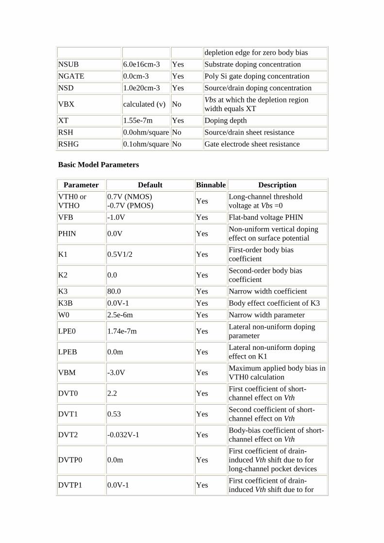
depletion edge for zero body bias
NSUB 6.0e16cm-3 Yes Substrate doping concentration
NGATE 0.0cm-3 Yes Poly Si gate doping concentration
NSD 1.0e20cm-3 Yes Source/drain doping concentration
VBX calculated (v) No Vbs at which the depletion region width equals XT
XT 1.55e-7m Yes Doping depth
RSH 0.0ohm/square No Source/drain sheet resistance
RSHG 0.1ohm/square No Gate electrode sheet resistance
Basic Model Parameters
Parameter Default Binnable Description
VTH0 or VTHO
0.7V (NMOS) -0.7V (PMOS)
Yes Long-channel threshold voltage at Vbs =0
VFB -1.0V Yes Flat-band voltage PHIN
PHIN 0.0V Yes Non-uniform vertical doping effect on surface potential
K1 0.5V1/2 Yes First-order body bias coefficient
K2 0.0 Yes Second-order body bias coefficient
K3 80.0 Yes Narrow width coefficient
K3B 0.0V-1 Yes Body effect coefficient of K3
W0 2.5e-6m Yes Narrow width parameter
LPE0 1.74e-7m Yes Lateral non-uniform doping parameter
LPEB 0.0m Yes Lateral non-uniform doping effect on K1
VBM -3.0V Yes Maximum applied body bias in VTH0 calculation
DVT0 2.2 Yes First coefficient of short-channel effect on Vth
DVT1 0.53 Yes Second coefficient of short-channel effect on Vth
DVT2 -0.032V-1 Yes Body-bias coefficient of short-channel effect on Vth
DVTP0 0.0m Yes First coefficient of drain-induced Vth shift due to for long-channel pocket devices
DVTP1 0.0V-1 Yes First coefficient of drain-induced Vth shift due to for

long-channel pocket devices
DVT0W 0.0 Yes First coefficient of narrow width effect on Vth for small channel length
DVT1W 5.3e6m-1 Yes Second coefficient of narrow width effect on Vth for small channel length
DVT2W -0.032V-1 Yes Body-bias coefficient of narrow width effect for small channel length
U0 0.067m2/(Vs) (NMOS); 0.025 m2/(Vs) (PMOS)
Yes Low-field mobility
UA 1.0e-9m/V for MOBMOD=0 and 1; 1.0e-15m/V for MOBMOD=2
Yes Coefficient of first-order mobility degradation due to vertical field
UB 1.0e-19m2/V2 Yes Coefficient of second-order mobility degradation due to vertical field
UC
-0.0465V-1 for MOB-MOD=1; -0.0465e-9 m/V2 for MOBMOD=0 and 2
Yes Coefficient of mobility degradation due to body-bias effect
EU 1.67 (NMOS); 1.0 (PMOS) No Exponent for mobility degradation of MOBMOD=2
VSAT 8.0e4m/s Yes Saturation velocity
A0 1.0 Yes Coefficient of channel-length dependence of bulk charge effect
AGS 0.0V-1 Yes Coefficient of Vgs dependence of bulk charge effect
B0 0.0m Yes Bulk charge effect coefficient for channel width
B1 0.0m Yes Bulk charge effect width offset
KETA -0.047V-1 Yes Body-bias coefficient of bulk charge effect
A1 0.0V-1 Yes First non-saturation effect parameter
A2 1.0 Yes Second non-saturation factor
WINT 0.0m No Channel-width offset parameter
LINT 0.0m No Channel-length offset parameter

DWG 0.0m/V Yes Coefficient of gate bias dependence of Weff
DWB 0.0m/V1/2 Yes Coefficient of body bias dependence of Weff bias dependence
VOFF -0.08V Yes Offset voltage in subthreshold region for large W and L
VOFFL 0.0mV No Channel-length dependence of VOFF
MINV 0.0 Yes Vgsteff fitting parameter for moderate inversion condition
NFACTOR 1.0 Yes Subthreshold swing factor
ETA0 0.08 Yes DIBL coefficient in subthreshold region
ETAB -0.07V -1 Yes Body-bias coefficient for the subthreshold DIBL effect
DSUB DROUT Yes DIBL coefficient exponent in subthreshold region
CIT 0.0F/m2 Yes Interface trap capacitance
CDSC 2.4e-4F/m2 Yes Coupling capacitance between source/drain and channel
CDSCB 0.0F/(Vm2) Yes Body-bias sensitivity of CDSC
CDSCD 0.0(F/Vm2) Yes Drain-bias sensitivity of DCSC
PCLM 1.3 Yes Channel-length modulation parameter
PDIBLC1 0.39 Yes Parameter for DIBL effect on Rout
PDIBLC2 0.0086 Yes Parameter for DIBL effect on Rout
PDIBLCB 0.0V-1 Yes Body bias coefficient of DIBL effect on Rout
DROUT 0.56 Yes Channel-length dependence of DIBL effect on Rout
PSCBE1 4.24e8V/m Yes First substrate current induced body-effect parameter
PSCBE2 1.0e-5m/V Yes Second substrate current induced body-effect parameter
PVAG 0.0 Yes Gate-bias dependence of Early voltage
DELTA ( in equation)
0.01V Yes Parameter for DC Vdseff
FPROUT 0.0V/m 0.5 Yes Effect of pocket implant on

Rout degradation
PDITS 0.0V-1 Yes Impact of drain-induced Vth shift on Rout.
PDITSL 0.0m-1 No Channel-length dependence of drain-induced Vth shift for Rout.
PDITSD 0.0V-1 Yes Vds dependence of drain-induced Vth shift for Rout
Parameters for Asymmetric and Bias-Dependent Rds Model
Parameter Default Binnable Description
RDSW 200.0 ohm( µ m)WR
Yes Zero bias LLD resistance per unit width for RDSMOD=0
RDSWMIN 0.0 ohm( µ m)WR
No LDD resistance per unit width at high Vgs and zero Vbs for RDSMOD=0
RDW 100.0 ohm( µ m)WR
Yes Zero bias lightly-doped drain resistance Rd(v) per unit width for RDSMOD=1
RDWMIN 0.0 ohm( µ m)WR
No Lightly-doped drain resistance per unit width at high Vgs and zero Vbs for RDSMOD=1
RSW 100.0 ohm( µ m)WR
Yes Zero bias lightly-doped source resistance Rs(V) per unit width for RDSMOD=1
RSWMIN 0.0 ohm( µ m)WR
No Lightly-doped source resistance per unit width at high Vgs and zero Vbs for RDSMOD=1
PRWG 1.0V-1 Yes Gate-bias dependence of LDD resistance
PRWB 0.0V-0.5 Yes Body-bias dependence of LDD resistance
WR 1.0 Yes Channel-width dependence parameter of LDD resistance
NRS 1.0 No Number of source diffusion squares
NRD 1.0 No Number of drain diffusion squares
Impact Ionization Current Model Parameters
Parameter Default Binnable Description
ALPHA0 0.0Am/V Yes First parameter of impact ionization current
ALPHA1 0.0A/V Yes Isub parameter for length scaling
BETA0 30.0V Yes The second parameter for impact ionization current
Gate-Induced Drain Leakage Model Parameters
Parameter Default Binnable Description
AGIDL 0.0ohm Yes Pre-exponential coefficient for GIDL

BGIDL 2.3e9V/m Yes Exponential coefficient for GIDL
CGIDL 0.5V3 Yes Parameter for body-bias effect on GIDL
DGIDL 0.8V Yes Fitting parameter for band bending for GIDL
Gate Dielectric Tunneling Current Model Parameters
Parameter Default Binnable Description
AIGBACC 0.43 (F s 2/ g )0.5m-1 Yes Parameter for Igb in accumulation
BIGBACC 0.054 (F s 2/ g )0.5 m-1V-1
Yes Parameter for Igb in accumulation
CIGBACC 0.075V-1 Yes Parameter for Igb in accumulation
NIGBACC 1.0 Yes Parameter for Igb in accumulation
AIGBINV 0.35 (F s 2/ g )0.5m-1 Yes Parameter for Igb in inversion
BIGBINV 0.03 (F s 2/ g )0.5m-1V-1 Yes Parameter for Igb in inversion
CIGBINV 0.0006V-1 Yes Parameter for Igb in inversion
EIGBINV 1.1V Yes Parameter for Igb in inversion
NIGBINV 3.0 Yes Parameter for Igb in inversion
AIGC 0.054 (NMOS) and 0.31 (PMOS) (F s 2/ g )0.5m-1
Yes Parameter for Igcs and Igc d
BIGC 0.054 (NMOS) and 0.024 (PMOS) (F s 2/ g )0.5 m-1V-1
Yes Parameter for Igcs and Igcd
CIGC 0.075 (NMOS) and 0.03(PMOS) V-1
Yes Parameter for Igcs and Igcd
AIGSD 0.43 (NMOS) and 0.31 (PMOS) (F s 2/ g )0.5 m-1
Yes Parameter for Igs and Igd
BIGSD 0.054 (NMOS) 0.024 (PMOS) (F s 2/ g )0.5 m-1V-1
Yes Parameter for Igs and Igd
CIGSD 0.075 (NMOS) and 0.03 (PMOS) V-1
Yes Parameter for Igs and Igd
DLCIG LINT Yes Source/drain overlap length for Igs and Igd
NIGC 1.0 Yes Parameter for Igcs , Igcd , Igs and Igd
POXEDGE 1.0 Yes Factor for the gate oxide thickness in source/drain overlap regions
PIGCD 1.0 Yes Vds dependence of Igcs and Igcd
NTOX 1.0 Yes Exponent for the gate oxide ratio
TOXREF 3.0e-9m No Nominal gate oxide thickness for gate dielectric tunneling current model only

Charge and Capacitance Model Parameters
Parameter Default Binnable Description
XPART 0.0 No Charge partition parameter
CGSO calculated (F/m)
No Non LDD region source-gate overlap capacitance per unit channel width
CGDO calculated (F/m)
No Non LDD region drain-gate overlap capacitance per unit channel width
CGBO 0.0 (F/m) No Gate-bulk overlap capacitance per unit channel length
CGSL 0.0F/m Yes Overlap capacitance between gate and lightly-doped source region
CGDL 0.0F/m Yes Overlap capacitance between gate and lightly-doped source region
CKAPPAS 0.6V Yes Coefficient of bias-dependent overlap capacitance for the source side
CKAPPAD CKAPPAS Yes Coefficient of bias-dependent overlap capacitance for the drain side
CF calculated (F/m)
Yes Fringing field capacitance
CLC 1.0e-7m Yes Constant term for the short channel model
CLE 0.6 Yes Exponential term for the short channel model
DLC LINT (m) No Channel-length offset parameter for CV model
DWC WINT (m) No Channel-width offset parameter for CV model
VFBCV -1.0V Yes Flat-band voltage parameter (for CAPMOD=0 only)
NOFF 1.0 Yes CV parameter in Vgsteff,CV for week to strong inversion
VOFFCV 0.0V Yes CV parameter in Vgsteff,CV for week to strong inversion
ACDE 1.0m/V Yes Exponential coefficient for charge thickness in CAPMOD=2 for accumulation and depletion regions
MOIN 15.0 Yes Coefficient for the gate-bias dependent surface potential
High-Speed/RF Model Parameters
Parameter Default Binnable Description
XRCRG1 12.0 Yes Parameter for distributed channel-resistance effect for both intrinsic-input resistance and charge-deficit NQS models

XRCRG2 1.0 Yes Parameter to account for the excess channel diffusion resistance for both intrinsic input resistance and charge-deficit NQS models
RBPB 50.0ohm No Resistance connected between bNodePrime and bNode
RBPD 50.0ohm No Resistance connected between bNodePrime and dbNode
RBPS 50.0ohm No Resistance connected between bNodePrime and sbNode
RBDB 50.0ohm No Resistance connected between dbNode and dbNode
RBSB 50.0ohm No Resistance connected between sbNode and bNode
GBMIN 1.0e-12mho
No
Conductance in parallel with each of the five substrate resistances to avoid potential numerical instability due to unreasonably too large a substrate resistance
Flicker and Thermal Noise Model Parameters
Parameter Default Binnable Description
NOIA 6.25e41 (eV)-1s1-EFm-3 for NMOS; 6.188e40 (eV)-1s1-EFm-3 for PMOS
No Flicker noise parameter A
NOIB 3.125e26 (eV)-1s1-EFm-1 for NMOS; 1.5e25 (eV)-1s1-EFm-1 for PMOS
No Flicker noise parameter B
NOIC 8.75 (eV)-1S1-EFm No Flicker noise parameter C
EM 4.1e7V/m No Saturation field
AF 1.0 No Flicker noise exponent
EF 1.0 No Flicker noise frequency exponent
KF 0.0 A2-EFs1-EFF No Flicker noise coefficient
NTNOI 1.0 No Noise factor for short-channel devices for TNOIMOD=0 only
TNOIA 1.5 No Coefficient of channel-length dependence of total channel thermal noise
TNOIB 3.5 No Channel-length dependence parameter for channel thermal noise partitioning
Layout-Dependent Parasitics Model Parameters
Parameter Default Binnable Description

DMCG 0.0m No Distance from S/D contact center to the gate edge
DMCI DMCG No Distance from S/D contact center to the isolation edge in the channel-length direction
DMDG 0.0m No Same as DMCG but for merged device only
DMCGT 0.0m No DMCG of test structures
NF 1 No Number of device figures
DWJ DWC (in CVmodel)
No Offset of the S/D junction width
MIN 0 No Whether to minimize the number of drain or source diffusions for even-number fingered device
XGW 0.0m No Distance from the gate contact to the channel edge
XGL 0.0m No Offset of the gate length due to variations in patterning
NGCON 1 No Number of gate contacts
Asymmetric Source/Drain Junction Diode Model Parameters
Parameter Default Binnable Description
IJTHSREV IJTHSREV=0.1A No Limiting current in reverse bias region
IJTHDREV IJTHDREV= IJTHSREV
No Limiting current in reverse bias region
IJTHSFWD IJTHSFWD=0.1A No Limiting current in forward bias region
IJTHDFWD IJTHDFWD= IJTHSFWD
No Limiting current in forward bias region
XJBVS XJBVS=1.0 No Fitting parameter for diode breakdown
XJBVD XJBVD=XJBVS No Fitting parameter for diode breakdown
BVS BVS=10.0V No Breakdown voltage
BVD BVD=BVS No Breakdown voltage
JSS JSS=1.0e-4A/m2 No Bottom junction reverse saturation current density
JSD JSD=JSS No Bottom junction reverse saturation current density
JSWS JSWS=0.0A/m No Isolation-edge sidewall reverse saturation current density
JSWD JSWD=JSWS No Isolation-edge sidewall reverse saturation current density
JSWGS JSWGS=0.0A/m No Gate-edge sidewall reverse saturation current density
JSWGD JSWGD=JSWGS No Gate-edge sidewall reverse saturation

current density
CJS CJS=5.0e-4 F/m2 No Bottom junction capacitance per unit area at zero bias
CJD CJD=CJS No Bottom junction capacitance per unit area at zero bias
MJS MJS=0.5 No Bottom junction capacitance grading coefficient
MJD MJD=MJS No Bottom junction capacitance grading coefficient
MJSWS MJSWS=0.33 No Isolation-edge sidewall junction capacitance grading coefficient
MJSWD MJSWD=MJSWS No Isolation-edge sidewall junction capacitance grading coefficient
CJSWS CJSWS=5.0e-10 F/m
No Isolation-edge sidewall junction capacitance per unit area
CJSWD CJSWD=CJSWS No Isolation-edge sidewall junction capacitance per unit area
CJSWGS CJSWGS=CJSWS No Gate-edge sidewall junction capacitance per unit length
CJSWGD CJSWGD=CJSWS No Gate-edge sidewall junction capacitance per unit length
MJSWGS MJSWGS=MJSWS No Gate-edge sidewall junction capacitance grading coefficient
MJSWGD MJSWGD=MJSWS No Gate-edge sidewall junction capacitance grading coefficient
PBS PBS=1.0V No Bottom junction built-in potential
PBD PBD=PBS No Bottom junction built-in potential
PBSWS PBSWS=1.0V No Isolation-edge sidewall junction built-in potential
PBSWD PBSWD=PBSWS No Isolation-edge sidewall junction built-in potential
PBSWGS PBSWGS=PBSWS No Gate-edge sidewall junction built-in potential
PBSWGD PBSWGD=PBSWS No Gate-edge sidewall junction built-in potential
Temperature Dependence Parameters
Parameter Default Binnable Description
TNOM 27° C No Temperature at which parameters are extracted
UTE -1.5 Yes Mobility temperature exponent

KT1 -0.11V Yes Temperature coefficient for threshold voltage
KT1L 0.0Vm Yes Channel length dependence of the temperature coefficient for threshold voltage
KT2 0.022 Yes Body-bias coefficient of Vth temperature effect
UA1 1.0e-9m/V Yes Temperature coefficient for UA
UB1 -1.0e-18 (m/V 2 ) Yes Temperature coefficient for UB
UC1 0.067V-1 for MOBMOD=1; 0.025m/V2 for MOBMOD=0 and 2
Yes Temperature coefficient for UC
AT 3.3e4m/s Yes Temperature coefficient for saturation velocity
PRT 0.0ohm-m Yes Temperature coefficient for Rdsw
NJS, NJD NJS=1.0; NJD=NJS No Emission coefficients of junction for source and drain junctions, respectively
XTIS, XTID
XTIS=3.0; XTID=XTIS No Junction current temperature exponents for source and drain junction, respectively
TPB 0.0V/K No Temperature coefficient of PB
TPBSW 0.0V/K No Temperature coefficient of PBSW
TPBSWG 0.0V/K No Temperature coefficient of PBSWG
TCJ 0.0K-1 No Temperature coefficient of CJ
TCJSW 0.0K-1 No Temperature coefficient of CJSW
TCJSWG 0.0K-1 No Temperature coefficient of CJSWG
dW and dL Parameters
Parameter Default Binnable Description
WL 0.0mWLN No Coefficient of length dependence for width offset
WLN 1.0 No Power of length dependence of width offset
WW 0.0mWWN No Coefficient of width dependence for width offset
WWN 1.0 No Power of width dependence of width offset
WWL 0.0 No Coefficient of length and width cross term

mWWN+WLN dependence for width offset
LL 0.0mLLN No Coefficient of length dependence for length offset
LLN 1.0 No Power of length dependence for length offset
LW 0.0mLWN No Coefficient of width dependence for length offset
LWN 1.0 No Power of width dependence for length offset
LWL 0.0 mLWN+LLN
No Coefficient of length and width cross term dependence for length offset
LLC LL No Coefficient of length dependence for CV channel length offset
LWC LW No Coefficient of width dependence for CV channel length offset
LWLC LWL No Coefficient of length and width cross-term dependence for CV channel length offset
WLC WL No Coefficient of length dependence for CV channel width offset
WWC WW No Coefficient of width dependence for CV channel width offset
WWLC WWL No Coefficient of length and width cross-term dependence for CV channel width offset
Range Parameters for Model Application
Parameter Default Binnable Description
LMIN 0.0m No Minimum channel length
LMAX 1.0m No Maximum channel length
WMIN 0.0m No Minimum channel width
WMAX 1.0m No Maximum channel width
Star-Hspice Manual - Release 2001.2 - June 2001