lh351b - amazon s3 · the lh351b suitable use in a broad range of applications features &...
TRANSCRIPT

1#
Product Family Data Sheet Rev. 13a 2018. 01. 17
High Power LED Series 3535 Ceramic Hot Binning
LH351B For Korean Market
High efficacy and high quality color rendering makes the LH351B suitable use in a broad range of applications
Features & Benefits
Operates at a maximum current of up to 1.5 A
Uniform light distribution under any beam angle
80 CRI makes it well suited for most applications
Hot binning @ 85 ºC
Completed 10,000 hours of LM-80 testing @ 1 A, 105 ºC
Applications
Indoor Lighting: Spotlight, Downlight
Outdoor Lighting: Street Light, Tunnel Light, Security Light, Parking Lot Light
Industrial Lighting: High Bay Light, Low Bay Light
Consumer Lighting: Torch Light

2
Table of Contents
1. Characteristics ----------------------- 3
2. Product Code Information ----------------------- 6
3. Typical Characteristics Graphs ----------------------- 11
4. Outline Drawing & Dimension ----------------------- 13
5. Reliability Test Items & Conditions ----------------------- 14
6. Soldering Conditions ----------------------- 15
7. Tape & Reel ----------------------- 16
8. Label Structure ----------------------- 18
9. Packing Structure ----------------------- 19
10. Precautions in Handling & Use ----------------------- 21

3
1. Characteristics
a) Absolute Maximum Rating
Item Symbol Rating Unit Condition
Operating Temperature Topr -40 ~ +105 ºC Note 1)*
Storage Temperature Tstg -40 ~ +120 ºC -
LED Junction Temperature Tj 150 ºC -
Forward Current IF 1500 mA -
Peak Pulse Forward Current IFP 2000 mA Duty 1/10 pulse width 10ms
Assembly Process Temperature
260 <10
ºC s
-
ESD (HBM) - ±5 kV -
Notes:
1) Refer to the derating curve, ‘3. Typical Characteristics Graph’, for proper driving current that maintained below maximum
junction temperature.

4
b) Electro-optical Characteristics
Item Unit Nominal CCT
(K)
Condition Value Typ. IF (mA) Tj (°C)
Luminous Flux (Φv) lm 5000
(75 CRI)
350 25 175
350 85 160
700 85 292
1000 85 391
1500 85 525
Forward Voltage (VF) V
350 25 2.86
350 85 2.75
700 85 2.89
1000 85 2.99
1500 85 3.12
Reverse Voltage (@ 5 mA)
V 350 25 14~19.5
Thermal Resistance (junction to solder point)
ºC/W 350 25 4
Beam Angle º 350 25 120
Notes:
1) Samsung maintains measurement tolerance of: luminous flux = ±7 %, forward voltage = ±0.1 V
2) Characteristics @ 25 °C are for reference only

5
c) Luminous Flux Characteristics (Tj = 85 ºC)
Nominal CCT (K)
CRI (Ra)
Min.1)
Sorting @ 350 mA (lm) Calculated Minimum Flux2)
(lm)
Flux Rank Flux Min.1)
@ 700 mA @ 1000 mA @ 1500 mA
5000
75
M3
(N3)
140 (153)
252
(276)
335
(366)
457
(499)
N3
(P3)
150 (164)
270
(295)
359
(392)
489
(534)
P3
(Q3)
160 (174)
288
(312)
382
(415)
518
(562)
80
K3
(M3)
130
(142)
234
(256)
311
(340)
424
(463)
M3
(N3)
140
(153)
252
(276)
335
(366)
457
(499)
N3
(P3)
150
(164)
270
(295)
359
(392)
489
(534)
5700
75
M3
(N3)
140 (153)
252
(276)
335
(366)
457
(499)
N3
(P3)
150 (164)
270
(295)
359
(392)
489
(534)
P3
(Q3)
160 (174)
288
(312)
382
(415)
518
(562)
80
K3
(M3)
130
(142)
234
(256)
311
(340)
424
(463)
M3
(N3)
140
(153)
252
(276)
335
(366)
457
(499)
N3
(P3)
150
(164)
270
(295)
359
(392)
489
(534)
(value in bracket): Minimum luminous flux @ 25 °C, for reference only
Notes:
1) Samsung maintains measurement tolerance of: luminous flux = ±7 %, CRI = ±3
2) Calculated minimum flux values are for reference only

6
2. Product Code Information
1 2 3 4 5 6 7 8 9 10 11 12 13 14 15 16 17 18
S P H W H 1 L 3 D 3 0 D D 4 R T M 3
Digit PKG Information Code Specification
1 2 3 Samsung Package High Power SPH
4 5 Color WH White
6 Product Version 1
7 8 Product L3 LH351 Series
9 Lens Type D Dome lens
10 Internal Code 3
11 Not Defined 0 Default
12 CRI & Sorting Temperature D Min. 75 85℃
13 14 Forward Voltage (V) D 4 2.6~3.0 Bin
Code:
D2 2.6~2.8
F2 2.8~3.0
15 16 CCT (K)
R T 5000 Bin
Code:
R1, R2, R3, R4
Q T 5700 Q1, Q2, Q3, Q4
K 3 130-160 K1 130-140
M 3 140~170 M1 140~150 K3
N 3 150~180 N1 150~160 M3
P 3 160-190 P1 160~170 N3
Q1 170~180 P3
R1 180-190
Digit 17: Min. spec.
Digit 18: The number of higher bin(s) from min. spec.
e.g.: M1 = 140~150 lm, M3 = 140~170 lm

7
a) Luminous Flux Bins (IF = 350 mA, Tj = 85 ºC)
Nominal CCT (K)
CRI (Ra) Min.
Product Code Flux Rank Flux Bin Flux Range
(Φv, lm)
5000
75
SPHWH1L3D30DD4RTM3 M3
M1 140 ~ 150
N1 150 ~ 160
P1 160 ~ 170
SPHWH1L3D30DD4RTN3 N3
N1 150 ~ 160
P1 160 ~ 170
Q1 170 ~ 180
SPHWH1L3D30DD4RTP3 P3
P1 160 ~ 170
Q1 170 ~ 180
R1 180 ~ 190
80
SPHWH2L3D30ED4RTK3 K3
K1 130 ~ 140
M1 140 ~ 150
N1 150 ~ 160
SPHWH2L3D30ED4RTM3 M3
M1 140 ~ 150
N1 150 ~ 160
P1 160 ~ 170
SPHWH2L3D30ED4RTN3 N3
N1 150 ~ 160
P1 160 ~ 170
Q1 170 ~ 180

8
a) Luminous Flux Bins (IF = 350 mA, Tj = 85 ºC)
Nominal CCT (K)
CRI (Ra) Min.
Product Code Flux Rank Flux Bin Flux Range
(Φv, lm)
5700
75
SPHWH1L3D30DD4QTM3 M3
M1 140 ~ 150
N1 150 ~ 160
P1 160 ~ 170
SPHWH1L3D30DD4QTN3 N3
N1 150 ~ 160
P1 160 ~ 170
Q1 170 ~ 180
SPHWH1L3D30DD4QTP3 P3
P1 160 ~ 170
Q1 170 ~ 180
R1 180 ~ 190
80
SPHWH2L3D30ED4QTK3 K3
K1 130 ~ 140
M1 140 ~ 150
N1 150 ~ 160
SPHWH2L3D30ED4QTM3 M3
M1 140 ~ 150
N1 150 ~ 160
P1 180 ~ 190
SPHWH2L3D30ED4QTN3 N3
N1 150 ~ 160
P1 160 ~ 170
Q1 170 ~ 180
b) Color Bins (IF = 350 mA, Tj = 85 ºC)

9
Nominal CCT (K)
CRI (Ra) Min.
Product Code Color Rank Chromaticity Bins
5000 75
SPHWH1L3D30DD4RTM3
RT (ANSI Bin)
R1, R2, R3, R4 SPHWH1L3D30DD4RTN3
SPHWH1L3D30DD4RTP3
5700 75
SPHWH1L3D30DD4QTM3
QT (ANSI Bin)
Q1, Q2, Q3, Q4 SPHWH1L3D30DD4QTN3
SPHWH1L3D30DD4QTP3
c) Voltage Bins (IF = 350 mA, Tj = 85 ºC)
Nominal CCT (K)
CRI (Ra) Min.
Product Code Voltage Rank Voltage Bin Voltage Range
(V)
- - - D4
D2 2.6 ~ 2.8
F2 2.8 ~ 3.0

10
d) Chromaticity Region & Coordinates (IF = 350 mA, Tj = 85 ºC)
Region CIE x CIE y Region CIE x CIE y Region CIE x CIE y Region CIE x CIE y
R rank (5000 K) Q rank (5700 K)
R1
0.3371 0.3490
R2
0.3451 0.3554
Q1
0.3215 0.3350
Q2
0.3290 0.3417
0.3451 0.3554 0.3533 0.3620 0.3290 0.3417 0.3371 0.3490
0.3440 0.3427 0.3515 0.3487 0.3290 0.3300 0.3366 0.3369
0.3366 0.3369 0.3440 0.3427 0.3222 0.3243 0.3290 0.3300
R3
0.3376 0.3616
R4
0.3463 0.3687
Q3
0.3207 0.3462
Q4
0.3290 0.3538
0.3463 0.3687 0.3551 0.3760 0.3290 0.3538 0.3376 0.3616
0.3451 0.3554 0.3533 0.3620 0.3290 0.3417 0.3371 0.3490
0.3371 0.3490 0.3451 0.3554 0.3215 0.3350 0.3290 0.3417
Note:
Samsung maintains measurement tolerance of: Cx, Cy = ±0.005

11
3. Typical Characteristics Graphs
a) Spectrum Distribution (IF = 350 mA, Tj = 85 ºC)
b) Forward Current Characteristics (Tj = 85 ºC)
c) Temperature Characteristics (IF = 350 mA)

12
d) Color Shift Characteristics (IF = 350 mA, Tj = 85 ºC)
e) Derating Curve and Beam Angle Characteristics (IF = 350 mA, Tj = 25 ºC)

13
4. Outline Drawing & Dimension
Notes:
1) This LED has built-in ESD protection device(s) connected in parallel to LED chip(s).
2) The thermal pad is electrically isolated from the anode and cathode contact pads.
3) Ts point and measurement method:
① Measure the nearest point to thermal pad as shown above. If necessary, remove PSR of PCB to reach Ts point.
② All pads must be soldered to the PCB to dissipate heat properly, otherwise the LED can be damaged.
Precautions:
1) Pressure on the LEDs will influence to the reliability of the LEDs. Precautions should be taken to avoid strong pressure on
the LEDs. Do not put stress on the LEDs during heating.
2) Re-soldering should not be done after the LEDs have been soldered. If re-soldering is unavoidable, LED`s characteristics
should be carefully checked before and after such repair.
3) Do not stack assembled PCBs together. Since materials of LEDs is soft, abrasion between two PCB assembled with LED
might cause catastrophic failure of the LEDs.
Measurement unit: mm
Tolerance: ±0.13 mm
Recommended Soldering Pattern
Anode
Cathode

14
5. Reliability Test Items & Conditions
a) Test Items
Test Item Test Condition Test
Hour / Cycle Sample Size
Room Temperature Life Test
25 ºC, DC Derating IF 1000 h 22
High Temperature Life Test
85 ºC, DC Derating IF 1000 h 22
High Temperature Humidity Life Test
85 ºC, 85 % RH, DC Derating IF 1000 h 22
Low Temperature Life Test
-40 ºC, DC Derating IF 1000 h 22
Damp Heat Cycling -10 ºC ↔ 25 ºC 95 % RH ↔ 65 ºC 95 % RH
DC Derating IF, 24 h / 1 cycle 10 cycles 11
Powered Temperature Cycle -40 ºC / 85 ºC each 20 min, 100 min transfer
power on/off each 5 min, DC Derating IF 100 cycles 11
Temperature Cycling -45 ºC / 15 min ↔ 125 ºC / 15 min temperature change within 5 min
500 cycles 100
High Temperature Storage
120 ºC 1000 h 11
Low Temperature Storage
-40 ºC 1000 h 11
ESD (HBM)
R1: 10 MΩ
R2: 1.5 kΩ
C: 100 pF
V: ±5 kV
5 times 30
ESD (MM)
R1: 10 MΩ
R2: 0
C: 200 pF
V: ±0.5 kV
5 times 30
Vibration Test 20~2000~20 Hz, 200 m/s
2, sweep 4 min
X, Y, Z 3 direction, each 1 cycle 4 cycles 11
Mechanical Shock Test 1500 g, 0.5 ms
3 shocks each X-Y-Z axis 5 cycles 11
b) Criteria for Judging the Damage
Item Symbol Test Condition
(Tj = 25 ºC)
Limit
Min. Max.
Forward Voltage VF IF = 350 mA Init. Value * 0.9 Init. Value * 1.1
Luminous Flux Φv IF = 350 mA Init. Value * 0.7 Init. Value * 1.1

15
6. Soldering Conditions
a) Reflow Conditions (Pb free)
Reflow frequency: 2 times max.
b) Manual Soldering Conditions
Not more than 5 seconds @ max. 300 ºC, under soldering iron.

16
7. Tape & Reel
a) Taping Dimension
(unit: mm)
Taping Direction

17
b) Reel Dimension
(unit: mm)
Notes:
1) Quantity: The quantity/reel is 1,000 pcs
2) Cumulative tolerance: Cumulative tolerance / 10 pitches is ±0.2 mm
3) Adhesion strength of cover tape: Adhesion strength is 0.1-0.7 N when the cover tape is turned off from the carrier tape at
10° angle to the carrier tape
4) Packaging: P/N, Manufacturing data code no. and quantity are indicated on the aluminum packing bag

18
Bin Code
D2R1M1
SPHWH2L3D30DD4RTM3 D2R1M1 IIIIIIIIIIIIIIIIIIIIIIIIIIIIIIIIIIIIIIIIIIIIIIIII GLAY94001 / I001 / 1,000 pcs
IIIIIIIIIIIIIIIIIIIIIIIIIIIIIIIIIIIIIIIIII
D2R1M1
SPHWH2L3D30DD4RTM3 D2R1M1 IIIIIIIIIIIIIIIIIIIIIIIIIIIIIIIIIIIIIIIIIIIIIIIII ①②③④⑤⑥⑦⑧⑨/Iⓐⓑⓒ/ 1,000 pcs
IIIIIIIIIIIIIIIIIIIIIIIIIIIIIIIIIIIIIIIIII
Lot Number
Product Code
8. Label Structure
a) Label Structure
Note: Denoted bin code and product code above is only an example (see description on page 7)
Bin Code:
ⓐⓑ: Forward Voltage bin (refer to page 8
ⓒⓓ: Chromaticity bin (refer to page 9)
ⓔⓕ: Luminous Flux bin (refer to page 7)
b) Lot Number
The lot number is composed of the following characters:
①②③④⑤⑥⑦⑧⑨ / Iⓐⓑⓒ / 1,000 pcs
①, ② : Production site (G3: Shenzhen, China, G4: Guangzhou, China, GB : Nanchang, China)
③ : Product state (A: Normal, B: Bulk, C: First Production, R: Reproduction, S: Sample)
④ : Year (Y: 2014, Z: 2015, A: 2016, …)
⑤ : Month (1~9, A, B, C)
⑥ : Day (1~9, A, B~V)
⑦⑧⑨ : Product serial number (001 ~ 999)
ⓐⓑⓒ : Reel number (001 ~ 999)
ⓐⓑⓒⓓⓔⓕ
19
D2R1M1
SPHWH2L3D30DD4RTM3 D2R1M1 IIIIIIIIIIIIIIIIIIIIIIIIIIIIIIIIIIIIIIIIIIIIIIIII GLAY94001 / I001 / 1,000 pcs
IIIIIIIIIIIIIIIIIIIIIIIIIIIIIIIIIIIIIIIIII
D2R1M1
SPHWH2L3D30DD4RTM3 D2R1M1 IIIIIIIIIIIIIIIIIIIIIIIIIIIIIIIIIIIIIIIIIIIIIIIII GLAY94001 / I001 / 7,000 pcs
IIIIIIIIIIIIIIIIIIIIIIIIIIIIIIIIIIIIIIIIII
D2R1M1
SPHWH2L3D30DD4RTM3 D2R1M1 IIIIIIIIIIIIIIIIIIIIIIIIIIIIIIIIIIIIIIIIIIIIIIIII GLAY94001 / I001 / 1,000 pcs
IIIIIIIIIIIIIIIIIIIIIIIIIIIIIIIIIIIIIIIIII
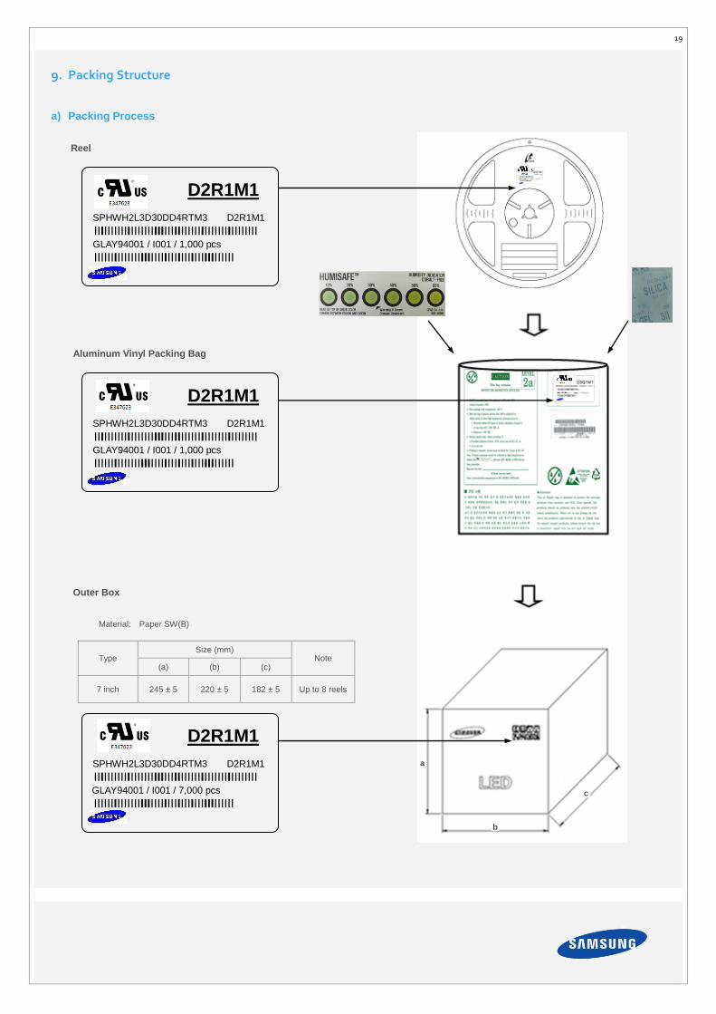
9. Packing Structure
a) Packing Process
Material: Paper SW(B)
Type Size (mm)
Note (a) (b) (c)
7 inch 245 ± 5 220 ± 5 182 ± 5 Up to 8 reels
Reel
Outer Box
Aluminum Vinyl Packing Bag
a
b
c

20
b) Aluminum Vinyl Packing Bag
c) Silica Gel & Humidity Indicator Card inside Aluminum Vinyl Bag
D2R1M1
SPHWH2L3D30DD4RTM3 D2R1M1 IIIIIIIIIIIIIIIIIIIIIIIIIIIIIIIIIIIIIIIIIIIIIIIII GLAY94001 / I001 / 1,000 pcs
IIIIIIIIIIIIIIIIIIIIIIIIIIIIIIIIIIIIIIIIII

21
10. Precautions in Handling & Use
1) For over-current protection, users are recommended to apply resistors connected in series with the LEDs to mitigate
sudden change of the forward current caused by shift of forward voltage.
2) This device should not be used in any type of fluid such as water, oil, organic solvent, etc. When cleaning is required, IPA
is recommended as the cleaning agent. Some solvent-based cleaning agent may damage the silicone resins used in the
device.
3) When the device is in operation, the forward current should be carefully determined considering the maximum ambient
temperature and corresponding junction temperature.
4) LEDs must be stored in a clean environment. If the LEDs are to be stored for three months or more after being shipped
from Samsung, they should be packed with a nitrogen-filled container (shelf life of sealed bags is 12 months at
temperature 0~40 ºC, 0~90 % RH).
5) After storage bag is opened, device subjected to soldering, solder reflow, or other high temperature processes must be:
a. Mounted within 672 hours (28 days) at an assembly line with a condition of no more than 30 ºC / 60 % RH, or
b. Stored at <10 % RH
6) Repack unused devices with anti-moisture packing, fold to close any opening and then store in a dry place.
7) Devices require baking before mounting, if humidity card reading is >60 % at 23 ± 5 ºC.
8) Devices must be baked for 1 hour at 60 ± 5 ºC, if baking is required.
9) The LEDs are sensitive to the static electricity and surge current. It is recommended to use a wrist band or anti-
electrostatic glove when handling the LEDs. If voltage exceeding the absolute maximum rating is applied to LEDs, it may
cause damage or even destruction to LED devices. Damaged LEDs may show some unusual characteristics such as
increase in leakage current, lowered turn-on voltage, or abnormal lighting of LEDs at low current.
10) VOCs (Volatile Organic Compounds) can be generated from adhesives, flux, hardener or organic additives used in
luminaires (fixtures). Transparent LED silicone encapsulant is permeable to those chemicals and they may lead to a
discoloration of encapsulant when they exposed to heat or light. This phenomenon can cause a significant loss of light
emitted (output) from the luminaires. In order to prevent these problems, we recommend users to know the physical
properties of materials used in luminaires and they must be carefully selected.

Legal and additional information.
About Samsung Electronics Co., Ltd.
Samsung Electronics Co., Ltd. inspires the world and shapes the future
with transformative ideas and technologies, redefining the worlds of TVs,
smartphones, wearable devices, tablets, cameras, digital appliances,
printers, medical equipment, network systems and semiconductors.
We are also leading in the Internet of Things space through, among others,
our Digital Health and Smart Home initiatives. We employ 307,000 people
across 84 countries. To discover more, please visit our official website at
www.samsung.com and our official blog at global.samsungtomorrow.com.
Copyright © 2016 Samsung Electronics Co., Ltd. All rights reserved.
Samsung is a registered trademark of Samsung Electronics Co., Ltd.
Specifications and designs are subject to change without notice. Non-metric
weights and measurements are approximate. All data were deemed correct
at time of creation. Samsung is not liable for errors or omissions. All brand,
product, service names and logos are trademarks and/or registered trademarks
of their respective owners and are hereby recognized and acknowledged.
Samsung Electronics Co., Ltd.
1, Samsung ro
Giheung-gu
Yongin-si, Gyeonggi-do, 17113
KOREA
www.samsungled.com