light emitting diodes and optically stimulated ...maajournal.com/issues/2015/vol15-2/full20.pdf ·...
TRANSCRIPT
Mediterranean Archaeology and Archaeometry, Vol. 15, No 2,(2015), pp. 277-291 Copyright © 2015 MAA
Open Access. Printed in Greece. All rights reserved.
DOI: 10.5281/zenodo.18058
LIGHT EMITTING DIODES AND OPTICALLY STIMULATED LUMINESCENCE DATING
IN ARCHAEOLOGY: AN OVERVIEW
Ioannis Liritzis 1, Nikolaos Droseros 2
1Laboratory of Archaeometry, University of the Aegean, Dept of Mediterranean Studies, 1 Demokratias Str, Rhodes 85100, Greece
2University of Patras, Dept of Physics, Rion 26500, Greece
Received: 15/03/2015 Accepted: 30/05/2015 Corresponding author: Ioannis Liritzis ([email protected])
ABSTRACT
Among the multiple applications of Light emitting diodes (LEDs), archaeology and earth sciences have benefited too concerning the determination of time (chronology) based on the thermoluminescene (TL) and optically stimulated luminescence (OSL) method of dating artifacts, material culture of archaeological and geoarchaeological significance. Blue Light emitting diodes (LED) is mostly used for stimulation and bleaching of luminescence, in lieu of green and IR LEDs. Ancient inorganic materials made of geological rocks (carving, knapping, mixing, firing) are either fired in antiquity above 450o C or sun exposed for a short time (surface luminescence dating) and thus the electron traps are completely bleached for the “zero time” clock to set up. The importance of blue LEDs in archaeology was the research product of 2014 Nobel Prize in Physics. On the occasion of blue LED invention and Nobel Prize we offer an extended overview of the development of semiconductor physics focused on LEDs (blue, green, IR) and linked to the principles of OSL dating in archaeology.
KEYWORDS: Luminescence, LED, chronology, semiconductors, dopants, archaeology, nobel prize, blue green IR light.
278 LIRITZIS & DROSEROS
Mediterranean Archaeology and Archaeometry, Vol. 15, No 2, (2015), pp. 277-291
1. INTRODUCTION
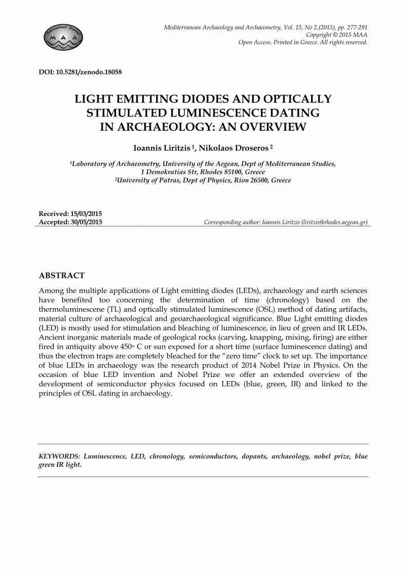
The Nobel Prize in Physics 2014 was awarded jointly to Isamu Akasaki, Hiroshi Amano and Shuji Nakamura "for the invention of efficient blue light-emitting diodes which has enabled bright and energy-saving white light sources". When they produced bright blue light beams from their semi-conductors in the early 1990s (Akasaki et al., 1992, 1993a, 1993b) they trig-gered a fundamental transformation of lighting technology. Red and green diodes had been around for a long time but without blue light, white lamps could not be created. Despite con-siderable efforts, both in the scientific communi-ty and in industry, the blue LED had remained a challenge for three decades. Thus, this devel-opment allowed for the creation of the white LED light sources that are inching toward ubiq-uity across the globe. Though LEDs of other colors have been around since the mid 1900s, the blue LED proved far more difficult to create as researchers struggled to find a material that would produce blue light. The three researchers recognized that gallium nitride would lead to a blue color and discovered a way to produce the light in an efficient way by adding in aluminum and indium. Figure 1 shows the structure of a modern LED. In the inset of the same Figure, the LT-buffer which enabled the growth of the GaN pure crystal is also shown.
Figure 1. Basic parts of a modern LED structure, in the insets are shown the recombination process between the p and n layers, the elements that consist the layers. In the
insets of the p-n junction and the additional LT-buffer layer, the use of which enabled the development of the
blue LED (based on Johan Jarnestad, The Royal Swedish Academy of Sciences)
Blue, green and red light needs to be com-bined to create white light, so the work of Akasaki, Amano, and Nakamura provided the final piece to a long-running puzzle. Since then, white LED lights have increased in effi-ciency and are slowly becoming more preva-lent. "The LED lamp holds great promise for in-creasing the quality of life for over 1.5 billion people around the world who lack access to electricity grids", The Royal Swedish Academy of Sciences explains, "due to low power requirements it can be powered by cheap local solar power".
Taking into account that about 25 ± 5% of the world's electricity is consumed by lighting, the wide and protracted adoption of LEDs signifi-cantly reduces the world's energy consumption and, with it, its emission of CO2 into the atmos-phere. In device physics and materials science the production of light-emitting diodes that could shine blue light was an expected follow-up of red and green, IR LEDs that were availa-ble by late 1960s. The advent of the first lumi-nous blue LED, which took place in 1993, com-pleted the visual spectrum.
A wide range of potential applications, from domestic, industrial lighting to optical storage, have emerged.
Below we give a brief account of the physics of LEDs and link their application as light stim-ulated sources in the luminescence (TL, OSL) method of chronology for reconstructing the past human evolution. This review is also initi-ated for the celebration of the current interna-tional year of light.
2. THE PHYSICS OF LEDS: A TUTORIAL
Following the course of the time since the be-ginnings of the 20th century, when electrolumi-nescence from a solid state material, namely a silicon carbide (SiC) crystal, was first observed by Henry Joseph Round (Round, 1907), until nowadays, a whole revolution in production and manipulation of light has been held. Silicon Carbide was just one of the many solid state materials that would play a key role both to the development of a whole new source of light and also to the development of computers. This new source of light, which was named as Light Emit-ting Diode or LED, with applications in many fields such as Technology, Communications,
LIGHT EMITTING DIODES AND OSL DATING IN ARCHAEOLOGY: AN OVERVIEW 279
Mediterranean Archaeology and Archaeometry, Vol. 15, No 2, (2015), pp. 277-291
Biology, Medicine, Culture, Archaeometry and everyday life, spurred many scientists to find the physical phenomenon which underlies the production of monochromatic light from solid state materials, and opened a new field in Phys-ics, named Optoelectronics or Photonics.
The main difference between conventional light sources and LEDs is the way by which the light is produced. Conventional materials, such as wolfram, need to be thermally activated in order to emit light. The production of light in these materials comes from thermal excitation and ionization of the electrons of their atoms, having random velocities and so they act like black bodies (see below).
The main characteristic of this type of radia-tion is the dependence of the maximum wave-length of the emitted radiation by the tempera-ture of the material. This is a characteristic that comes from the fact that black body’s radiation obeys to Planck’s distribution (Serway, 2005) (equation 1):
1
8),(
3
2
Tkhf Be
hf
c
fTfu
(1)
where h is the Planck’s constant, c is the speed of light, f is the frequency of the emitted radia-tion, T is the temperature of the material and kB is the Boltzmann’s constant. All materials, even the human body, obey to this law. The disad-vantages of the radiation which obeys the Planck’s distribution is the high energy needed for the heating of the material, the energy loss-es, which come from the fact that a high per-centage of the energy given to the material is consumed in ohmic heating of the material, the broad spectrum of the emitted radiation which forbids the production of monochromatic light, their large response time, the disability of fur-ther manipulation of the characteristics of the emitted light and finally their short lifetime (Li et al.,2014). So all these facts consider to the need to exempt from the conventional thermal techniques and seek for another way of produc-ing almost monochromatic, wave guided light, with tunable emission wavelength and power, as well as with high efficiency of energy con-version into light.
A type of materials, with properties different from liquids, gases, metals and dielectrics which enable the emission of light with all the desirable properties is needed. These materials are named semiconductors and their character-istic which makes them different from the con-ventional materials is the existence of two types of charge carriers, electrons and holes, as well as the statistics which governs their distribu-tion. Because of the importance of these materi-als, it was considered essential to mention some of their physical properties which enable their use in LEDs.
About 20 years after Round’s discovery, a new theory for the statistics of the fermions, and consequently of the carriers in solid state, was developed. It was Fermi-Dirac’s statistics which resulted to a new distribution for the probabil-ity of occupation of energy states of the charge carriers in these materials (equation 2).
)1(
1)(
/)(
TkEEFD
BFeEf (2)
where fFD(E) is the probability of occupation of a certain state with energy E, T is the tempera-ture, kB is the Boltzmann’s constant and EF is the energy of the Fermi level of the material.
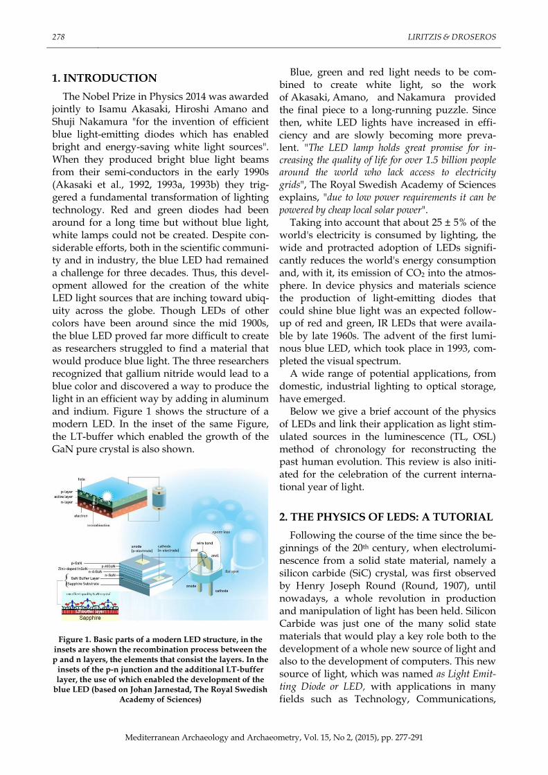
The impact of this distribution is the for-mation of two energy bands, one for the holes and one for the electrons, which are called the valence and the conduction band respectively. These bands are separated by an energy gap, Eg, which is a region that cannot be occupied by carriers. At T=0 K the valence band is filled and the conduction band is empty of electrons. Due to the Pauli’s principle these bands are further separated into zones, while these zones are fur-ther split because of the spin-orbit interaction. The conduction band remains unaffected, be-cause the total angular momentum (J) of its states is zero, while, as can be seen in Figure 2, the valence band gets splitted into two states, one with J=3/2 and one with J=1/2, correspond-ing to the heavy and light holes (Dyakonov, 2008). Additionally the presence of a relativistic phenomenon, which provokes the interaction of total angular momentum with the nuclear spin, results to the formation of a third zone which is called the split-off zone (Yu and Cardona, 1999).
280 LIRITZIS & DROSEROS
Mediterranean Archaeology and Archaeometry, Vol. 15, No 2, (2015), pp. 277-291
Figure 2. Band structure of semiconductors, donors and acceptors energy levels the energy band gap Eg=h.f, and the splitting of the valence band (based on (Li et al.,2014)
Depending on which type of carriers is in ma-jority, semiconductors are characterized as n-type, when electrons dominate, or p-type, when holes dominate (Sze, 1985).
An interesting characteristic of semiconduc-tors is the ability to change their type from n to p and vice versa according to a process which is known as doping. During this process the semi-conductor is injected with positive or negative ions which act as acceptors or donors of elec-trons. Acceptors trap the electrons which ther-mally escape from the valence band resulting to a minority of electrons in the conduction band, while donors replenish the conduction band with more electrons resulting to a majority of electrons in the conduction band compared to the holes of the valence band. Donors and ac-ceptors occupy energy states into the band gap. The states of the donors lie below the conduc-tion band and the states of the acceptors above the valence band (Shklovskii, and Efros, 1984; Redfield and Bube, 1996). The presence of other atoms in the semiconductor or other lattice im-perfections results to the deflection of the crys-tal from its perfect structure and the loss of the desirable properties (in analogy to natural min-erals used for luminescence, see below). Every deflection from the perfect structure of the crys-tal is characterized as a defect. There are many types of defects that can be formed depending on the technique of the crystal growth and the process of doping. These defects form addition-al energy states into the band gap in similar
ways with the donors and acceptors while they can act as traps reducing the quantum yield of the radiative recombination (Redfield et al., 1996).
Thanks to the huge progress of technology, it is possible to interfere and change the types and concentration of dopants and defects on will, giving to the materials the desirable properties according to the needs of every application. The finding of the right combination of materials as well as the proper dopants is a difficult proce-dure and this is the reason that the discovery of LEDs emitting in the blue spectral region took place almost a century after H. J. Round’s dis-covery.
After this short introduction to semiconduc-tors Physics it is easier to take a deeper look to the function of LEDs. The basic element behind LEDs function is a contact of two semiconduc-tors, each one with different majority carriers, named p-n junction. Actually the p-n junction is not formed by simply bringing the two materi-als in touch, but it is a more complicated pro-cess. Some of the available techniques are mo-lecular beam epitaxy, chemical vapor deposi-tion, wafer bonding, metal-organic vapor phase epitaxy, pulsed laser deposition and liquid phase epitaxy (Grundmann, 2006). Molecular beam epitaxy technique was invented by Cho and Arthur in 1975 (Cho et al., 1975; Joyce, 1990)
and it is the most popular technique for the manufacturing of solid state heterostructures because it allows the control of crystal growth at the atomic level and the manipulation of the surface composition and morphology. During this process, heating coils made of the desirable elements are placed into effusion cells. The heating coils get thermally ionized and the ions are guided by a mass spectrometer until they impinge on a heated substrate film, while the whole process takes place under high vacuum (Schubert, 1993).
As soon as the p-n junction is formed, and with absence of external field, electrons start flowing from the n-type towards the p-type semiconductor until the Fermi levels of the two materials equalize and finally the carriers are at equilibrium. The final result of this procedure is the bending of the conduction and valence bands of both materials, as it is shown in Figure 3a. The formation of the p-n junction results to

LIGHT EMITTING DIODES AND OSL DATING IN ARCHAEOLOGY: AN OVERVIEW 281
Mediterranean Archaeology and Archaeometry, Vol. 15, No 2, (2015), pp. 277-291
the formation of a depletion region between the two semiconductors, by the same way that a depletion region is formed when a metal comes in touch with an insulator. In order to exempt from this equilibrium state, so as to keep the electrons flowing and recombining with holes,
an external voltage needs to be applied on the edges of the junction. Figure 3b shows the fur-ther bending of the zones of the two materials when current flows through the junction (Li et al.,2014).
Figure 3: Energy diagram showing the orientation of the band zones when (a) there is no current flow and (b) when currents flow through the p-n junction e-and positive carriers h+ in opposite direction
Voltage is another important parameter by which the characteristics of the output light can be manipulated and this fact was already known by the experiments of H. J. Round, who had observed the change at the emission wave-length of the silicon carbide crystal, which was provoked by changing the voltage on its edges from ten to one hundred Volts (Round, 1907). Of course the magnitude of the voltage needed has been reduced over the years and nowadays a few Volts are enough for the junction to start emitting light. The relation which connects the applied voltage and the current which flows through an ideal p-n junction is Shockley’s equation (Blanc et al., 1964) (equation 3).
1exp
Tk
eVII
B
o (3)
where Io is the saturation current, e is the elec-tronic scharge, V is the applied voltage, kB is the Boltzmann’s constant and T is the temperature.
The initial generation of LEDs was made of SiC and ZnS semiconductors, and emission from SiC in the blue region was possible with an efficiency of less than 0.005%. The following generation of LEDs was mainly based on GaAs and included III–V compound semiconductors (Blanc et al., 1964; Hall et al., 1962; Cusano,
1964). The latter were constructed by vapour or liquid phase epitaxy, and their emission wave-length was in the infrared region (870 – 980 nm) (Schubert, 1993). It has taken a lot of research effort on the combination of materials and do-pants to reach the development of the first Al-GaAs (Rupprecht, 1967) and GaAsP (Holonyak et al., 1963) LEDs emitting in the red spectral region. During the same period, green and red emitting LEDs that were made of nitrogen doped GaP and oxygen doped GaP, respective-ly, were developed. Thus, the first demonstra-tion of a yellow emitting LED took place in 1972 (Craford, et al., 1972). In this way a large part of the visible and infrared spectrum was covered, but the blue spectral region remained inaccessi-ble disabling the production of white light, as its production needs the mixing of red, green and blue colors, as shown in Fig. 4.
Figure 4: The production of white light by the mixing of the basic colors
The basic difficulty in the development of a blue emitting LED was the finding of the suita-

282 LIRITZIS & DROSEROS
Mediterranean Archaeology and Archaeometry, Vol. 15, No 2, (2015), pp. 277-291
ble technique by which the p-type material of the junction would be formed. GaN had already been selected as the suitable material since 1973 by the teams of Akasaki and Amano of Nagoya University (Ohki, 1974) and Nakamura of Nichia Chemicals, because of its large energy band gap which corresponds to the ultraviolet spectral region but at that time the growth of single crystals of this material was too difficult. Another difficult task was to turn GaN, which is an n-type material, into p-type. In 1979, it was decided that the most suitable technique for the development of GaN single crystal was Metalorganic Vapor Phase Epitaxy (MOVPE). Finally, after a lot of research the first perfect GaN crystal was grown in 1985 at Nagoya Uni-versity, thanks to H. Amano (Koide et al., 1986). Thus, the development of the p-type crystals AlGaN and GaInN (Akasaki et al., 1992; Khan et al. 1986; Amano et al., 1988; Akasaki et al., 1981; Murakami et al., 1991) and the further im-provement of the growth technique of GaN by S. Nakamura (Nakamura et al., 1992, 1993; Nakamura, Mukai et al., 1993) culminated with the efficient blue emitting LEDs with its distinct spectrum in comparison to green, yellow and red/IR spectra and in contrast to blackbody spectra (Fig. 5). The photons of the emitted light have higher energies than the excitation pho-tons in order to avoid measurement of ordinary photoluminescence (according to Stokes law or shift, see Fig.11 below).
Figure 5: (a) Radiation from a black body and (b)
Spectral output from LEDs with different emission wavelengths, the central wavelength of the output of
each LED is shown in the inset.
The unlimited applications of LEDs in Tech-nology have provoked a need for simplified models in order to be easy for the non experts to understand the basic principles of their Physics, operation, maintenance and safe usage and there are many technical handbooks written and simplified models developed for this pur-pose.
Amongst the multiple applications of LEDs is the use as stimulated agent for the determina-tion of time of rock minerals by luminescence techniques.
Below we give a short chronicle of LEDs used in OSL dating, the rationale of luminescence dating that indeed results to a hallmark of LEDs in quite accurate quantitative archaeological dating, and preceding basics of luminescence mechanism based on the lattice defects.
3. LATTICE DEFECTS IN MINERALS
The basics of luminescence light phenomenon are based on the energy gaps and associated point defects and competition between traps and holes (luminescent centers) in natural min-eral insulators such as quartz (SiO2 + impuri-ties), feldspar, zircon, calcite. Excitation of at-oms that are responsible for luminescence in mineral crystals is made by heat or monochro-matic radiation of LEDs. The presence of defects in the silica matrix can dramatically change its structural, electrical, and optical proper-ties(Curie, 1963; Kittel, 2005; McKeever, 1985).
The emission of light happens when an excit-ed electron derived from the conduction band, with a discrete energy state transition, falls into the valence band and recombines with a hole. The frequency of the emitted light is deter-mined by the energy band gap Eg=E2-E1 (Fig.2). In fact, the photon will have an angular fre-quency ω and energy (= hv, where h is the Planck constant and v is the frequency (equa-tion 4).
(4) where is the reduced Planck constant (=h/2π) (Williams and Hall, 1978).
According to Randall-Wilkins model the TL intensity I(t) is given (equation 5):
I(t) = - (dn/dt) = n Sexp(-E/kT) (5) where n(cm-3) the electron concentration trapped at time t(s), k (eVK-1) is the Boltzmann’s constant, S(sec-1) is the frequency factor and T(K) is the temperature. If the sample is heated up so that T rises at a linear heating rate β=dT/dt (Ks-1), then (equation 6)
dn/n = -(S/β)exp(-E/kT)dT (6)
The relevant mathematical expressions for thermoluminescence (TL) are derived for differ-ent models (e.g. Rnadall-Wilkins, May-Partridge, Garlic-Gibson) with transitions that
LIGHT EMITTING DIODES AND OSL DATING IN ARCHAEOLOGY: AN OVERVIEW 283
Mediterranean Archaeology and Archaeometry, Vol. 15, No 2, (2015), pp. 277-291
are strictly localized, where transitions are via a band; and where transitions are by overlap transfer. Analytical expressions follow from as-sumptions about the relative densities of trap-ping states, filled trapping states, and empty recombination states; and from assumptions about the relative values of the different transi-tion probabilities. Various types of lumines-cence are often identified according to the source of the energy which excites the emission.
The formation of defects (that may lead to the transformation of the existing defects to other types of defect) are caused by many parameters, such as the manufacturing processes, mechani-cal stress, change of temperature, the presence of impurities and irradiation. Usually, defects can be grouped according to their structure and size as point defects, plane defects and disloca-tions (linear defects) (Stevens-Kalceff et al., 1995; Kofstad, 1988). We consider two types of point defects; intrinsic or extrinsic. The Intrinsic point defects involve atoms of only the host ma-trix, i.e. vacancies (the host atoms are missing, Schottky defects or Frenkel pairs) and self-interstitials (additional host atoms at an intersti-tial position). The Extrinsic point defects in-volve atoms chemically different from the host crystal, such as those used for electrical doping. At any rate, in a perfect silica glass matrix the present defects could include silicon or oxygen vacancies and their interstitials, O−O or Si−Si homobonds or under-coordinated silicons or oxygens.
Since ancient times, the quartz (silicon diox-ide, SiO2) is the initial starter material for the production of silicate glasses and ceramics. It is distributed on a wide range in the natural envi-ronment, and is present in the form of sand on all rocks (sedimentary, metamorphic and vol-canic) in the lakes, coasts, deserts and Pleisto-cene age deposits. Quartz may occur in crystal-line or amorphous forms (e.g. obsidian), and is found in nature in impure forms, such as sand-stone, silica sand or quartz. The ceramic fabric result to a most frequently artifact unearthed from archaeological excavations and its typolo-gy offers a relative cultural stage to archaeolo-gists that study past cultures and relative chronological frames. The quantitative age cal-culation is obtained by TL or OSL with errors around ±3-7%. Quartz specific gravity and melt-
ing point depend on the crystalline structure. The silica is known to occur in many crystalline phases or modes (alpha-quartz, beta-quartz, al-pha-cristobalite, and others) besides some amorphous phases (opal, hyalite, natural silica glass etc.) (Fanderlik, 1991).
4. OSL DATING IN ARCHAEOLOGY & GEOSCIENCES
4.1 Basic principles
The luminescence from mineral insulators that are measured is usually derived from either quartz or feldspar sand-sized grains, or unsepa-rated silt-sized grains. There are advantages and disadvantages to using each. Quartz is the most abundant in rocks and lithic artifacts. For quartz one normally uses blue or green excita-tion and measures the near ultra-violet emis-sion, though these probe also feldspars too (Liritzis et al., 2008). For feldspar or silt-sized grains one normally uses near infra-red excita-tion and measures the violet emission.
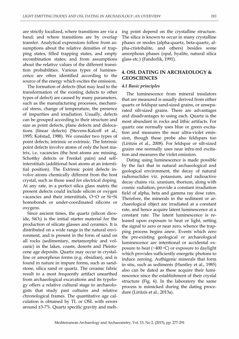
Dating using luminescence is made possible by the fact that in natural archaeological and geological environment, the decay of natural radionuclides viz. potassium, and radioactive decay chains viz. uranium, thorium, along with cosmic radiation, provide a constant irradiation field of alpha, beta and gamma ray dose rates. Therefore, the minerals in the sediment or ar-chaeological object are irradiated at a constant rate, and hence acquire latent luminescence at a constant rate. The latent luminescence is re-leased upon exposure to heat or light, setting the signal to zero or near zero, whence the trap-ping process begins anew. Events which zero the pre-existing geological or archaeological luminescence are intentional or accidental ex-posure to heat (~400 oC) or exposure to daylight which provides sufficiently energetic photons to induce zeroing. Authigenic minerals that form in situ, such as sediments (Huntley et al., 1985) also can be dated as these acquire their lumi-nescence since the establishment of their crystal structure (Fig. 6). In the laboratory the same process is mimicked during the dating proce-dure (Liritzis et al., 2013a).
284 LIRITZIS & DROSEROS
Mediterranean Archaeology and Archaeometry, Vol. 15, No 2, (2015), pp. 277-291
Figure 6a: Schematic diagram. Growth and resetting of the latent luminescence signal for dated (Liritzis et al.,
2013a).
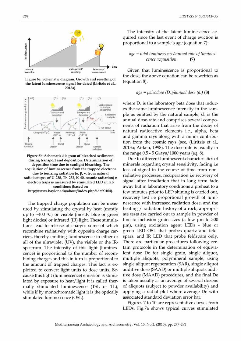
Figure 6b: Schematic diagram of bleached sediments during transport and deposition. Determination of
deposition time due to sunlight bleaching. The acquisition of luminescence from the trapped electrons
due to ionizing radiation (α, β, γ, from natural radioisotopes of U-238, Th-232, K-40, cosmic radiation) n
electron traps is measured by stimulated LED in lab conditions (based on
http://www.baylor.edu/about/index.php?id=90104).
The trapped charge population can be meas-ured by stimulating the crystal by heat (mostly up to ~400 oC) or visible (mostly blue or green light diodes) or infrared (IR) light. These stimula-tions lead to release of charges some of which recombine radiatively with opposite charge car-riers, thereby emitting luminescence in either or all of the ultraviolet (UV), the visible or the IR-spectrum. The intensity of this light (lumines-cence) is proportional to the number of recom-bining charges and this in turn is proportional to the amount of trapped charges. This fact is ex-ploited to convert light units to dose units. Be-cause this light (luminescence) emission is stimu-lated by exposure to heat/light it is called ther-mally stimulated luminescence (TSL or TL), while if by monochromatic light it is the optically stimulated luminescence (OSL).
The intensity of the latent luminescence ac-quired since the last event of charge eviction is proportional to a sample’s age (equation 7):
age = total luminescence/annual rate of lumines-
cence acquisition (7)
Given that luminescence is proportional to
the dose, the above equation can be rewritten as (equation 8),
age = paleodose (De)/annual dose (da) (8)
where De is the laboratory beta dose that induc-es the same luminescence intensity in the sam-ple as emitted by the natural sample, da is the annual dose-rate and comprises several compo-nents of radiation that arise from the decay of natural radioactive elements i.e., alpha, beta and gamma rays along with a minor contribu-tion from the cosmic rays (see, (Liritzis et al., 2013a; Aitken, 1998). The dose rate is usually in the range 0.5 - 5 Grays/1000 years (eq. 8).
Due to different luminescent characteristics of minerals regarding crystal sensitivity, fading i.e loss of signal in the course of time from non-radiative processes, recuperation i.e recovery of signal after irradiation that in long term fade away but in laboratory conditions a preheat to a few minutes prior to LED shining is carried out, recovery test i.e proportional growth of lumi-nescence with increased radiation dose, and the heating / radiation history of a rock, appropri-ate tests are carried out to sample in powder of fine to inclusion grain sizes (a few μm to 300 μm), using excitation agent LEDs - blue or green LED OSL that probes quartz and feld-spars, and IR LED that probe feldspars only. There are particular procedures following cer-tain protocols in the determination of equiva-lent dose De for single grain, single aliquot, multiple aliquots, polymineral sample, using single aliquot regeneration (SAR), single aliquot additive dose (SAAD) or multiple aliquots addi-tive dose (MAAD) procedures, and the final De is taken usually as an average of several dozens of aliquots (subject to powder availability) and applying a radial plot where average De with associated standard deviation error bar.
Figures 7 to 10 are representative curves from LEDs. Fig.7a shows typical curves stimulated

LIGHT EMITTING DIODES AND OSL DATING IN ARCHAEOLOGY: AN OVERVIEW 285
Mediterranean Archaeology and Archaeometry, Vol. 15, No 2, (2015), pp. 277-291
by blue of natural sample and irradiated with various beta particles doses, the recuperated signal and the determination of De with SAR, and Fig.7b another natural signal. The Fig.8 is typical curve by IR LEDs, and Fig.9 for green LED. Another De determination following the additive dose procedure in single aliquot pro-cedure, following standard protocol, is given in Fig.10 for granite comprised by 40% quartz, 25% biotite and phlogopite, 25% albite, 5% mi-crocline (K felsdpar) and 5% amphibole (Liritzis et al., 2013a).
Figure 7: a) OSL decay curves of quartz from limestones derived from a prehistoric settlement in Delphi, Greece, stimulated by blue LEDs for the natural signal (A), the
three incremental regenerative doses, (C to E respective-ly), the repeat dose point (B) and the recuperation after-wards (F), for the first 20 s of stimulation. Inset: Single
Aliquot Regeneration (SAR) growth curve, measured for an aliquot from the sample D4 after preheating at 220oC. Equivalent dose value is provided by interpolation of the natural normalised OSL signal (filled triangle) onto the
growth curve (line) resulting from the fit to the results of the measurement sequence (filled squares). Filled dot represents the recycle point value; the SAR ED value
yielded (line) is 18.9 G (Liritzis et al., 2014a).
Figure 7b: Natural luminescence of sample from Temple
SETI IV Abydos Egypt, with blue LED (Liritzis et al., 2013b).
Figure 8. Bleaching of granite powder from Mykerinus
pyramid. IR LED bleaching of prior irradiation with beta
dose of 23 Gray and preheating at 220C (Liritzis et al., 2014b).
Figure 9. Green LED of quartz. Number of photons per
shining time [Galloway et al., 1998].
Figure 10. Determination of equivalent dose for sample of granite from Osirion Temple at Abydos, Egypt, with
single aliquot blue OSLfor 0,1s after preheat at 220C for 60s.The corrected (due to crystal sensitivity change) De
(solid curve) is12.01.5Gy (Liritzis et al., 2014b).
Artifacts that can be dated include ceramics, burned lithics, burnt bricks and soil (e.g., from hearths), and potentially unburnt stone surfaces that were exposed to light and then buried. Ge-oarchaeological materials such as sediments that can be dated using luminescence include aeolian deposits (dune sands or loessic dust),

286 LIRITZIS & DROSEROS
Mediterranean Archaeology and Archaeometry, Vol. 15, No 2, (2015), pp. 277-291
paleosols, colluvial deposits, and water- and ice lain deposits (e.g. marine, fluvial, lacustrine) (Aitken, 1998; Roberts, 1997; Murray et al., 2002; Liritzis at al., 2000; Liritzis, 2002; Preusser et al., 2008; Fuchs et al., 2009). For all these annealed or bleached geoachaeological materials the ‘lu-minescence clock’ is set up that starts counting the time (Fig.6). Applications of luminescence methods for various geological domains were reviewed in a special issue of BOREAS (2008).
Application of luminescence in archaeology and anthropology were reviewed (Roberts, 1997; Galbraith et. al., 1999; Feathers, 2003; Rich-ter, 2007; Liritzis et al., 1999). These include da-ting of the burial context in archaeological de-posits, artifacts, such as ceramics, pot boilers, fireplaces, rock art, and wasp nests in caves, monuments and statues (Liritzis et al., 1999; Roberts et al., 1997) and an overview is present-ed in (Liritzis et al., 2013a). In all cases the “zero time” event represents either a incidental / de-liberate firing or sun exposure from some sec-onds to several hours and immediately overlaid by material that blocks sunlight to illuminate the original surface (surface dating) (Liritzis, 2010). Thereafter electrons are constantly filling traps, their quantity is a measure of lumines-cence or time elapsed since the ancient event. This way certain material culture and geoar-chaeological materials connected with human activities or other environmental events con-nected with human presence are chronological markers.
Sampling such materials follows sample preparation under laboratory conditions and extraction of fine grain (with diameter up to 30 μm) or inclusion grain sizes (several dozens of μm). Those are stimulated be monochromatic light. A sample in which the mineral grains have all been exposed to sufficient daylight (seconds for quartz; hundreds of seconds for feldspar) the bleaching is fast, electron-hole re-combination is made resulting to the emission of minute luminescence, and it can be said to be of zero age. As long as the electrons are kept trapped in deep energy levels, the older the sample is, the more electrons are trapped and more light it emits, up to a saturation limit. One may metaphorically see this phenomenon as a trapped light in the dark for thousands of years that is revealed in the lab.
5. HISTORICAL DEVELOPMENT OF LED IN OSL DATING
The LEDs used for OSL stimulation in lumi-nescence dating are usually blue, green, and IR with most use of blue LEDs.
Optical stimulation of luminescence is usual-ly achieved using an array of LEDs, which are compact, fast and enables electronic control of the illumination power density. The standard Riso system at Denmark (http://osl.risoe.dk) incorporates continuous wave (CW), as well as, linear modulation (LM)-OSL or pulsed OSL stimulation. The array of LEDs is equipped with an optical feedback servo-system to ensure the stability of the stimulation power. The LEDs are arranged in 7 clusters each containing 7 LEDs (i.e. a total of 49 LEDs). The distance between the diodes and the sample is approximately 20 mm.
Thus, for example, an array of blue light emitting diodes (LEDs, 470±30 nm), has been used for stimulation, emitting 40-50mW/cm2at the position of the sample, accompanied by fil-ters of UV Schott BG39 + Hoya 340 nm and transmitting window 280-340 nm, FWHM of 20 nm, or a green pass filter (GG-420). For IRSL, the stimulation wavelength of diode is 875 (±40) nm and the maximum power of ~135-145 mW/cm2 with filters Blue Schott BG39 + Corn-ing 7-59, and transmitting window 340-480 nm.
The OSL detection measurement systems have been considerably improved over the past two decades (Botter-Jensen, 2003). In fact most OSL systems have been constructed from TL readers adapted to OSL (Galloway, 1991). At any rate the desire to develop a reader system for OSL measurement is due to the fact that OSL technology has advantages over TL im-posed by the high heating temperatures and has become the preferred mode of dosimetry, espe-cially with the advent of blue LEDS. The scat-tered stimulating photons from OSL by LEDs are excluded from the photomultiplier (PM) de-tecting the luminescence by using proper filters in front of the PM. The concept of OSL for da-ting application was firstly introduced by Hunt-ley et al. (1985) (Huntley et al., 1985), who used the green light from an argon ion laser as a light source. (Alternatives include xenon arc lamp and a halogen lamp employing optical filters to
LIGHT EMITTING DIODES AND OSL DATING IN ARCHAEOLOGY: AN OVERVIEW 287
Mediterranean Archaeology and Archaeometry, Vol. 15, No 2, (2015), pp. 277-291
select suitable stimulation wavelengths from a broad-band light source (Spooner et al., 1989; Botter-Jensen et al., 1992).
The blue LED system has also been devel-oped by Botter-Jensen et al. (1999)(Botter-Jensen et al., 1999) and Hong and Galloway (2000). In fact the former introduced an arrangement us-ing a phototransistor to detect the brightness of the light emitted by the diodes for providing feedback control to ensure a constant level of illumination of the sample. The latter offered a new assembly where the constancy of the level of illumination depended on the light intensity from the LEDs as determined by the current flowing through them, which is provided by a constant current supply. Chithambo (2011) de-scribed a somehow economical pulsed OSL sys-tem based on the blue and green LEDs.
Galloway (1992) introduced a compact ar-rangement of 16 green light emitting diodes (LEDs) for luminescence stimulation. The low power was compensated by increasing the measuring times, i.e., the duration of exposure to light from the LEDs, that as a result was a low ratio of luminescence signal to background, as well as a subsequent limitation on the threshold of detectable absorbed radiation dose from quartz or feldspar crystals. Galloway et al. (1997) reported a substantially improved green LED system for luminescence stimulation, which provides sensitivity comparable to that of the conventional argon ion laser system. In the luminescence dating process the samples in powder form to be dated must be exposed to ionizing radiation in order to plot the lumines-cence against the laboratory administered radia-tion dose, which enables the luminescence from the natural sample material to be interpreted as an equivalent dose. The radionuclide 90Sr/90Y is usually employed as a reference for the labora-tory radiation dose, though alternative radioac-tive source a small X-ray irradiator has been in-troduced by Hashimoto et al. (2002) [Hashimoto et al., 2002] with some advantages regarding choice of grain size penetration.
Recently a novel compact and economical OSL system comprising a precision x-y-z stage for loading 12 samples, a small X-ray generator for radiation dosing, and two high-density blue LEDs for optical stimulation equipped with VIS liquid light guides (VIS-LLGs), was developed
by Choi et al. (2014) (Choi et al., 2014), where emphasis is placed on aspects of the system’s design and performance that are novel or of particular importance, rather than on detailed comparisons with previously introduced sys-tems. Two high-density blue LEDs (model: LXHL-PB02) with forced air convection were used that have a power density of 15–25 mW/cm2 with a peak in the emission spectrum at 470 nm (full width at half maximum (FWHM) 20 nm). The 20 nm of FWHM is a half value of that of the Nichia green (NSPG-500) and blue (NSPB-500) LED previously intro-duced (Hong et al., 2000; Galloway et al, 1997; Jain et al., 2007). Each green long pass filter (Schott GG-420) was placed in front of the VIS LLGs combined with LEDs in order to remove the meddlesome tail of blue light (<400 nm), which can cause interference between the lumi-nescence and the stimulating light. In this sys-tem luminescence was detected through two 3 mm Hoya U-340 filters, one of which was coat-ed with metal oxide to attenuate the stray light from the transmission window found in the red region of a normal U-340 filter. The lumines-cence detection was achieved using an EMI 9235QB PM.
On the other hand, the OSL from green LEDs of different types produced by companies (Nichia, Toshiba, III-V) have been used, with λ between 525-565 nm and filters Red Komar IU and transmission window 650-750 nm (Liritzis et al., 2013a; Botter-Jensen et al., 1999a; 1999b), or a combination of HA3 and DUG11 optical filters (pass band about 310-380 nm and detect-ed by an EMI type 9635QA photomultiplier, with approx. power at sample 0.2 mW/cm2 (Galloway et al, 1997; 1993). Typical conditions used for OSL measurements after blue and oth-er LED bleaching are given elsewhere (Botter-Jensen, 2000; Yukihara and Mckeever, 2011; Liritzis et al. 2013a). It has been noticed that blue LEDs are more fre-quently used in quartz because they give higher accuracy in De and larger light output due to excitation wavelength.

288 LIRITZIS & DROSEROS
Mediterranean Archaeology and Archaeometry, Vol. 15, No 2, (2015), pp. 277-291
Figure 11. Excitation and emission spectral profiles that
indicate the principle of wavelength involved.
6. CONCLUSION
LEDs have played a major role in the lumi-nescence dating with most applications made
by blue LED. Though the luminescence mecha-nism is still developed, the basic solid state is-sues involved that refer to the quality properties of minerals (defects, irradiation and heating his-tories) are known at a satisfactory level, while the use of LEDs have replaced laser beams and due to their advantages (economic, light, little heating on sample) has revolutionized the ad-vent of OSL dating. Chronology of past human cultures has gained a great deal from the appli-cation of LEDs especially the blue LEDs. Thanks to the invention of blue LEDs their application to archaeological and geoarchaeological dating, of at least the past half a million years, has been significant.
ACKNOWLEDGEMENTS We thank the two anonymous referees for constructive comments.
REFERENCES
Aitken, M. J. (1985) Thermoluminescence Dating, Oxford Academic Press. Aitken, M. J., (1998) An introduction to Optical Dating, Oxford University Press, Oxford, UK. Akasaki, I., Amano, H., Koide, N., Kotaki, M. and Manabe, K. (1993a) Conductivity control of GaN
and fabrication of UV/blue GaN light emitting devices. Physica B, Vol. 185, 428. Akasaki, I., and Amano, H. (1992) Room temperature ultraviolet/blue light emitting devices based
on AlGaN/GaN multi-layered structure. Conference on Solid State Devices and Materials, Vol. 327.
Akasaki, I., Amano, H., Kito, M., and Hiramatsu, K. (1991) Photoluminescence of Mg-doped p-type GaN and electroluminescence of GaN p-n junction LED. Journal of Luminescence, Vol. 48 & 49, 666.
Akasaki, I., Amano, H., Murakami, H., Sassa, M., Kato, H. and Manabe, K. (1993b) Growth of GaN and AlGaN for UV/blue p-n junction diodes. Journal of Crystal Growth Journal of Crystal Growth, Vol. 128, 379.
Amano, H., Akasaki, I., Kozawa, T., Hiramatsu, K., Sawaki, N., Ikeda, K., and Ishii, Y. (1988) Elec-tron beam effect on blue luminescence of Zinc – doped GaN. Journal of Luminescence, Vol. 40&41, 121.
Blanc, J., Bube, R. H., and Weisberg, L. R. (1964) Behaviour of lattice defects in GaAs. J. Phys. Chem. Solids, Pergamon Press 25, Vol. 225.
Boreas. Special Issue: Luminescence dating of Quaternary sediments. Volume 37, Issue 4 Botter-Jensen, L., and Duller, G.A.T., Murray, A.S., and Banerjee, D. (1999a) Blue light emitting di-
odes for optical stimulation of quartz in retrospective dosimetry and dating. Radiat. Prot. Dosim., Vol. 84, 335-340.
Botter-Jensen, (2000) Development of optically stimulated luminescence techniques using natural minerals and ceramics, and their application to retrospective dosimetry. Riso-R-1211 (EN), 74–85.
Botter-Jensen, L., Andersen, C.E., Duller, G.A.T., Murray, A.S. (2003) Developments in radiation, stimulation, and observation facilities in luminescence measurements. Radiat. Meas., Vol. 37, p. 535.
LIGHT EMITTING DIODES AND OSL DATING IN ARCHAEOLOGY: AN OVERVIEW 289
Mediterranean Archaeology and Archaeometry, Vol. 15, No 2, (2015), pp. 277-291
Botter-Jensen, L., and Duller, G.A.T. (1992) A new system for measuring optically stimulated lu-minescence from quartz samples. Nucl. Tracks Radiat. Meas.,Vol. 20, 549.
Botter-Jensen, L., Mejdahl, V., and Murray, A.S. (1999) New light on OSL. Quat. Geochron., Vol. 18, 303.
Botter-Jensen, L., Mejdahl, V., and Murray, A.S. (1999b) New light on OSL. Quat. Sci. Rev., Vol. 18, 303.
Cho, A. Y., and Arthur, J. R. (1975) Molecular Beam Epitaxy. Progress in Solid-State Chemistry, Vol. 10, Part 3, 157-191.
Choi, J.H., Kim, M.J., Cheong, C.S., and Hong, D.G. (2014) Development of OSL system using two high-density blue LEDs equipped with liquid light guides. Nuclear Instruments and Meth-ods in Physics Research B, Vol. 323, 19.
Chithambo, M.L. (2011) A time-correlated photon counting system for measurement of pulsed op-tically stimulated luminescence. J. Lumin., Vol. 131, 92.
Craford, M. G., Shaw, R. W., Herzog, A. H., and Groves, W.O. (1972) Radiative recombination mechanisms in GaAsP diodes with and without nitrogen doping. J. Appl. Phys., Vol. 43, 4075.
Curie, J.D., (1963) Luminescence in Crystals. John Wiley Sons Inc., New York. Cusano, D.A. (1964) Radiative recombination from GaAs directly excited by electron beams. Solid
State Communications, Vol. 2, 353. Dyakonov, M.I. (2008), Spin Physics in Semiconductors. Springer Series in Solid-State Sciences, Vol.
157. Fanderlik, I., (1991) Silica Glass and its Application. Glass Science and Technology 11, ELSEVIER,
Amsterdam. Feathers, J. K. (2003) Use of luminescence dating in archaeology. Measurement Science and Technolo-
gy, Vol. 14, 1493. Fuchs, M., Lang, A. (2009) Luminescence dating of hillslope deposits – a review. Geomorphology,
Vol. 109, 17. Galbraith, R.F., Roberts, R.G., Laslett, G.M., Yoshida, H., and Olley, J.M. (1999) Optical dating of
single and multiple grains of quartz from Jinmium rock shelter, northern Australia: Part I, Experimental design and statistical models. Archaeometry, Vol. 41, 339.
Galloway, R.B. (1991) A versatile 40-sample system for TL and OSL investigations. Nucl. Tracks Ra-diat. Meas., Vol. 18, 265.
Galloway, R.B. (1992) Towards the use of green light emitting diodes for the optically stimulated luminescence dating of quartz and feldspar. Meas. Sci. Technol., Vol. 3, 330.
Galloway, R.B. (1993) Stimulation of luminescence using green light emitting diodes. Radiat. Prot. Dosim., Vol. 47, 679.
Galloway, R.B., Hong, D.G., and Napier, N.J. (1997) A substantially improved green-light-emitting diode system for luminescence determination. Meas. Sci. Technol., Vol. 8, 267.
Galloway, R.B., and Neal, M.A. (1998) Green light emitting diodes used in Luminescence. Ancient TL, Vol. 6, p. 1.
Grundmann, M., (2006) The Physics of Semiconductors. Springer-Verlag Berlin Heidelberg. Hall, R.N., Fenner, G. E., Kingsley, J. D., Soltys, T.J. and Carlson, R.O. (1962) Coherent light emis-
sion from GaAs junctions. Phys. Rev. Lett., Vol. 9, 366. Hashimoto, T., Nakagawa, T., Hong, D.G., and Takano, M. (2002) An automated system for both
red/blue thermoluminescence (TL) and optically stimulated luminescence (OSL) meas-urement. J. Nucl. Sci. Technol., Vol. 39, 108.
Holonyak, N. Jr., Bevacqua, S.F., Bielan, C.V., Carranti, F.A., Hess, B.G., and Lubowski, S.J. (1963) Electrical properties of Ga(As1-xPx) p-n junctions. Proceedings of the IEEE, Vol. 51, 2.
Hong, D.G., and Galloway, R.B. (2000) Comparison of equivalent dose values determined by lu-minescence stimulation using blue and green light. Nucl. Instr. Meth. Phys.Res. B, Vol. 160, 59.

290 LIRITZIS & DROSEROS
Mediterranean Archaeology and Archaeometry, Vol. 15, No 2, (2015), pp. 277-291
Huntley, D.J. , Godfrey-Smith, D.I., and Thewalt, M.L.W. (1985) Optical dating of sediments. Na-ture, Vol. 313, 105.
Jain, M., and Lindvold, L.R. (2007) Blue light stimulation and Linearly Modulated Optically Stimu-lated Luminescence. Ancient TL, Vol. 25, 2.
Joyce, B.A. (1990) Molecular beam epitaxy - fundamentals and current status. Contemporary Physics, Vol. 31, No 3, 195-197.
Khan, M. R. H., Koide, Y., Sawaki, N., and Akasaki, I. (1986) Behaviour of Zn as dopant in the pho-toluminescence of AlxGa1-xN. Solid State Communications, Vol. 57, 17.
Kittel, C. , (2005) Introduction to solid state physics 8th edition, John Wiley & Sons, Inc, NJ. Kofstad, P., (1988) High Temperature Corrosion. ELSEVIER, London and New York. Koide, Y., Itoh, H., Sawaki, N., Akasaki, I., and Hashimoto, M. (1986) Epitaxy growth of
AlxGa1−xN by MOVPE. Journal of the Electrochemical Society, Vol. 133, (9), 1956. Li, J., Wang, J., Liu, Z., and Poppe, A. (2014) Solid-State Physics Fundamentals of LED Thermal Behav-
io. In Lesance, C.J.M & Poppe, A (eds), Thermal management for LED applications. Ch.2, 15-52, Springer New York.
Liritzis, I., and Galloway, R.B. (1999) Dating implications from solar bleaching of thermolumines-cente of ancient marble. J Radioanal. Nucl. Chem., Vol. 241, 361.
Liritzis, I. (2000) Advances in thermo- and opto- luminescence dating of environmental materials (sedimentary deposits): part I: techniques. GLOBAL-NEST, vol.2, No 1, 3-27, also, part II: applications. GLOBAL-NEST, Vol.2, No 1, 29-49.
Liritzis, I., Galloway, R.B., Hong, D., and Kyparissi-Apostolika, N. (2002) OSL dating of three pre-historic ceramics from Theopetra cave, Greece: a case study. Mediterranean Archaeology & Archaeometry, Vol. 2, 35.
Liritzis, I., Kitis, G., Galloway, R.B., Vafiadou, A., Tsirliganis, N., and Polymeris, G. (2008) Probing luminescence dating of archaeologically significant carved rock types. Mediterranean Ar-chaeology & Archaeometry, Vol. 8, 61.
Liritzis, I. (2010) Strofilas (Andros Island, Greece): new evidence for the cycladic final neolithic pe-riod through novel dating methods using luminescence and obsidian hydration. Journal of Archaeological Science (Elsevier), Vol. 37, 1367.
Liritzis, I., Singhvi, A.K., Feathers, J.K., Wagner, G.A., Kadereit, A., Zacharias, N. and Li, S.-H., (2013a) Luminescence Dating in Archaeology, Anthropology and Geoarchaeology: An Overview. Springer Briefs in Earth System Sciences
Liritzis, I., et al. (2013b) Advances in surface luminescence dating : some new data from three se-lected Mediterranean sites. Mediterranean Archaeology & Archaeometry, Vol. 13, 105.
Liritzis, I., Aravantinos, V., Polymeris, G.S., Zacharias, N., Fappas, I., Agiamarniotis, G., Sfampa, I.K., Vafiadou, A., and Kitis, G., (2014) Witnessing prehistoric Delphi by luminescence da-ting. PALEVOL (Comptes Redues de l’ Academie des Sciences, Paris), in press.
Liritzis, I., and Vafiadou, A. (2014) Surface luminescence dating of some Egyptian monuments. Journal of Cultural Heritage. Journal of Cultural Heritage (in press)
McKeever, S.W.S , (1985) Thermoluminescence of solids. CUP, Cambridge. Murakami, H., Asahi, T., Amano, H., Hiramatsu, K., Sawaki, N., and Akasaki, I. (1991) Growth of
Si-doped A1xGa1-xN on (0001) sapphire substrate by metalorganic vapor phase epitaxy. Journal of Crystal Growth, Vol. 115, 648.
Murray, A.S., and Olley, J.M. (2002) Precision and accuracy in the optically stimulated lumines-cence dating of sedimentary quartz: a status review. Geochronometria, Vol. 21, 1.
Nakamura, S., Mukai, T., and Senoh, M. (1992) In situ monitoring and Hall measurements of GaN grown with GaN buffer layers. Journal of Applied Physics, Vol. 71, 5543.
Nakamura, S., Mukai, T., Senoh, M., Nagahama, S., and Iwasa, N. (1993) In x Ga(1−x)N/In y Ga(1−y)N superlattices grown on GaN films. Journal of Applied Physics, Vol. 74, 3911.
Nakamura, S., Senoh, M., and Mukai, T. (1993) Highpower InGaN/GaN double heterostructure violet light emitting diodes. Applied Physics Letters, Vol. 62, 2390.

LIGHT EMITTING DIODES AND OSL DATING IN ARCHAEOLOGY: AN OVERVIEW 291
Mediterranean Archaeology and Archaeometry, Vol. 15, No 2, (2015), pp. 277-291
Ohki, Y. , Asao, I., and Akasaki, I. (1974) Vapor phase epitaxial growth of Nitrogen-doped In1-xGaxP alloys. Journal of Crystal Growth,Vol. 24/25, 244
Preusser, F., Degering, D., Fuchs, M., Hilgers, A., Kadereit, A., Klasen, N., Krbetschek, M., Richter, D., and Spencer, J. (2008) Luminescence dating: basics, methods and applications. Quater-nary Science Journal, Vol. 57, 95.
Redfield, D., Bube, R., (1996) Photo-induced Defects in Semiconductors. Cambridge University Press. Richter, D. (2007) Advantages and limitations of thermoluminescence dating of heated flint from
paleolithic sites. Geoarchaeology, Vol. 22, 671. Roberts, R.G. (1997) Luminescence dating in archaeology: from origins to optical. Radiat. Meas.,
Vol. 27, 819. Roberts, R.G., Walsh, A., Murray, A., Olley, J., Jones, R., Morwood, M., Tuniz, C., Lawson, E.,
Macphail, M., Bowdery, D., and Naumann, I. (1997) Luminescence dating of rock art and past environments using mud-wasp nests in northern Australia. Nature, Vol. 387, 696.
Round, H. J. (1907) A note on Carborundum. Electrical World., Vol. 49, 309. Rupprecht, H., Woodall, J. M., and Pettit, G. D. (1967) Efficient visible electroluminescence at
300°K FROM Ga1x Al x As pn junctions grown by liquid phase epitaxy. Applied Physics Letters, Vol. 11, 81.
Schubert, E.F. (1993) Doping in III-V Semiconductors. Cambridge University Press. Serway, R.A., Moses, C.J. and Moyer, C.A., (2005), Modern Physics, 3rd edition, Thomson Learning
Inc., Belmont USA. Shklovskii, B.I. and Efros, A.L., (1984) Electronic Properties of Doped Semiconductors. Springer – Ver-
lag, Berlin Heidelberg. Sze, S.M., (1985) Semiconductor Devices Physics and Technology. Bell Telephone Laboratories Inc. Spooner, N.A., and Questiaux, D.G. (1989) Optical dating Achenheim beyond the Eemian using
green and infrared stimulation. in: Long and Short Range Limits in Luminescence Dating. RLAHA Occasional Publication, Vol. 9, 97.
Stevens-Kalceff, M.A., and Philips, M.R., (1995) Cathodoluminescence microcharacterization of the defect structure of quartz. Phys. Rev. B, Vol. 52, 3122.
Tilley, R. (2004) Understanding solids: The science of materials. John Willey and Sons LTD, Chichester Williams, F.W and Hall, R (1978) Luminescence and the light emitting diode. Pergamon Press, Oxford. Yu, P.Y., and Cardona, M. (1999) Fundamentals of Semiconductors, 3rd ed. Springer. Yukihara, E.G., and Mckeever S.W.S. (2011) Optically stimulated luminescence: fundamentals and ap-
plications. Wiley, Sussex, 362