linear constant current vcm driver -...
TRANSCRIPT
Product structure:Silicon monolithic integrated circuit This product is not designed protection against radioactive rays .
1/20
Datasheet
© 2012 ROHM Co., Ltd. All rights reserved. 01. Jul. 2013 Rev.004TSZ22111・14・001
www.rohm.com TSZ02201-0H2H0B600460-1-2
Linear Constant Current VCM Driver BU64241GWZ
General Description
The BU64241GWZ is designed to drive voice coil motor(VCM). The driver includes ISRC (intelligent slew rate control) to reduce mechanical ringing to optimize the camera’s auto focus capabilities.
Features 2.3 V min driver power supply Current sink output 10 bit resolution current control ISRC mechanical ringing compensation 2-wire serial interface Integrated current sense resistor
Applications Autofocus in mobile camera modules Driving VCM actuators
Key Specifications Power supply range Standby current Internal resistance Master clock Output maximum current
2.3 to 4.8 V0 µA (typ.)
1.5 Ω (typ.)400 kHz (typ.)130 mA (typ.)
Package
W (Typ.) ×D (Typ.) ×H (Max.)UCSP30L1 1.30 mm × 0.77 mm × 0.33 mm
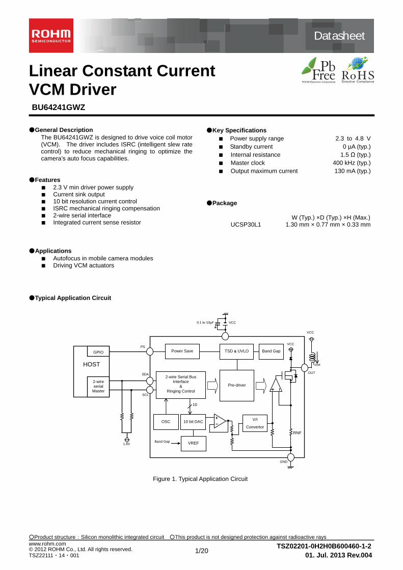
Typical Application Circuit
OUT
GND
10
VCC
VCC
V/I
Convertor
ISINK
SDA
VCC
SCL
Pre-driver
Band Gap
Band Gap
PS Power Save
RNF
0.1 to 10µF
TSD & UVLO
VREF
2-wire Serial Bus Interface
& Ringing Control
10 bit DACOSC
Figure 1. Typical Application Circuit
1.8V
HOST
2-wire serial
Master
GPIO
DatasheetDatasheet
2/20
BU64241GWZ
© 2012 ROHM Co., Ltd. All rights reserved. 01. Jul. 2013 Rev.004
www.rohm.com
TSZ22111・15・001 TSZ02201-0H2H0B600460-1-2
Pin Configuration
Figure 2. Pin configuration (TOP VIEW) Pin Description
Ball Name Function
PS Power save
SDA Serial data input
SCL Serial clock input
OUT Current output
GND Ground
VCC Power supply voltage
Block Diagram
1 2 3
A PS SDA SCL
B OUT GND VCC
Figure 3. Block Diagram
GND
OUT
10
VCC
VREF
2-wire serial Bus Interface
& Ringing Control
10 bit DACOSC V/I
Convertor
SDA
VCC
SCL Pre-driver
Band Gap
Band Gap
PS Power Save
RNF
TSD & UVLO
DatasheetDatasheet
3/20
BU64241GWZ
© 2012 ROHM Co., Ltd. All rights reserved. 01. Jul. 2013 Rev.004
www.rohm.com
TSZ22111・15・001 TSZ02201-0H2H0B600460-1-2
Absolute Maximum Ratings
Parameter Symbol Limit Unit
Power supply voltage VCC - 0.5 to + 5.5 V
Power save input voltage VPS - 0.5 to + 5.5 V
Control input voltage*1 VIN - 0.5 to + 5.5 V
Power dissipation Pd 220*2 mW
Operating temperature range Topr - 25 to + 85 °C
Junction temperature Tjmax 125 °C
Storage temperature range Tstg - 55 to + 125 °C
Output current IOUT + 200*3 mA
*1 VIN is 2-wire serial interface input pins (SCL, SDA) *2 UCSP30L1 package. Reduced by 2.2 mW/°C over 25 °C when mounted on a glass epoxy board (50 mm × 58 mm × 1.75 mm; 8 layers) *3 Must not exceed Pd, ASO, or Tjmax of 125 °C
Recommended Operating Ratings
Parameter Symbol Min. Typ. Max. Unit
Power supply voltage VCC 2.3 3.0 4.8 V
Power save input voltage VPS 0 - 4.8 V
Control input voltage*1 VIN 0 - 4.8 V
2-wire serial interface frequency FCLK - - 400 kHz
Output current IOUT - - 130*4 mA
*1 VIN is 2-wire serial interface input pins (SCL, SDA) *4 Must not exceed Pd, ASO
DatasheetDatasheet
4/20
BU64241GWZ
© 2012 ROHM Co., Ltd. All rights reserved. 01. Jul. 2013 Rev.004
www.rohm.com
TSZ22111・15・001 TSZ02201-0H2H0B600460-1-2
Electrical Characteristics (Unless otherwise specified Ta = 25 °C, VCC = 3.0 V)
Parameter Symbol Limit
Unit Conditions Min. Typ. Max.
Power Consumption
Standby current ICCST - 0 5 µA Power save pin = L = VPSL
Circuit current ICC - 0.6 1.0 mA Power save pin = H = VPSH 2-wire serial PS bit = 1, SCL = 400 kHz
Power Save Input (VPS = PS)
High level input voltage VPSH 1.26 - VCC V
Low level input voltage VPSL 0 - 0.5 V
High level input current IPSH - 10 - 10 µA VPS = 3 V
Low level input current IPSL - 10 - 10 µA VPS = 0 V
Control Input (VIN = SCL, SDA)
High level input voltage VINH 1.26 - VCC V
Low level input voltage VINL 0 - 0.5 V
Low level output voltage VINOL - - 0.4 V IIN = + 3.0 mA (SDA)
High level input current IINH - 10 - 10 µA Input voltage = 0.9 x VIN
Low level input current IINL - 10 - 10 µA Input voltage = 0.1 x VIN
Under Voltage Lock Out
UVLO voltage VUVLO 1.6 - 2.2 V
Master Clock
MCLK frequency MCLK - 5 - 5 % MCLK = 400 kHz
10 Bit D/A Converter (for Controlling Output Current)
Resolution DRES - 10 - bits
Differential nonlinearity DNL - 1 - 1 LSB
Integral nonlinearity INL - 4 - 4 LSB
Output Current Performance
Output current resolution IORES - 126 - µA Per 1 DAC code step
Output maximum current IOMAX 117 130 143 mA DAC_code = 0x3FF
Zero code offset current IOOFS 0 1 5 mA DAC_code = 0x000
Output voltage VOUT - 150 200 mV Output current = 100 mA
Maximum applied voltage VOMAX - - VCC V
Output resistance ROUT - 1.5 2.0 Ω
DatasheetDatasheet
5/20
BU64241GWZ
© 2012 ROHM Co., Ltd. All rights reserved. 01. Jul. 2013 Rev.004
www.rohm.com
TSZ22111・15・001 TSZ02201-0H2H0B600460-1-2
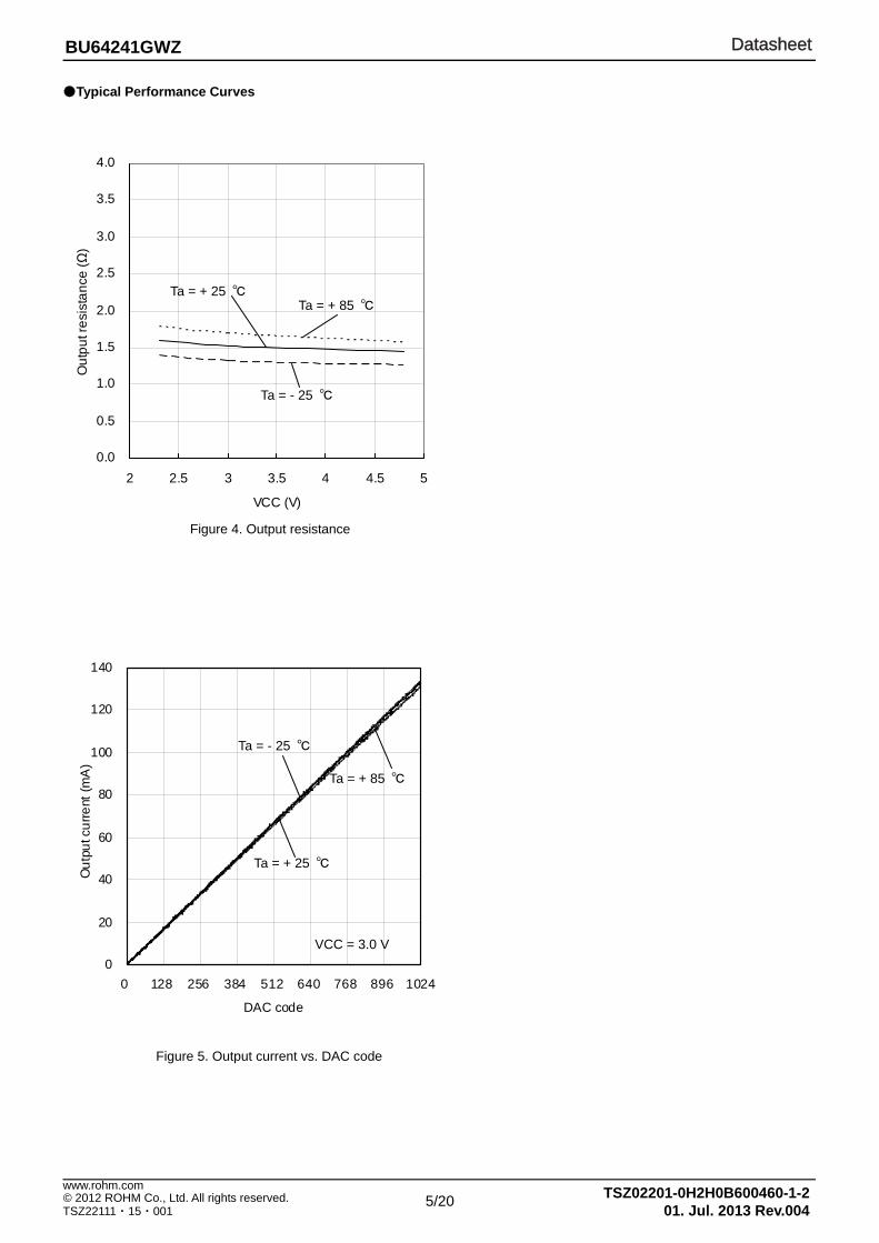
Typical Performance Curves
0
20
40
60
80
100
120
140
0 128 256 384 512 640 768 896 1024
DAC code
Out
put c
urre
nt (m
A)
Figure 4. Output resistance
Figure 5. Output current vs. DAC code
0.0
0.5
1.0
1.5
2.0
2.5
3.0
3.5
4.0
2 2.5 3 3.5 4 4.5 5
VCC (V)
Out
put r
esis
tanc
e (Ω
)
Ta = + 85 Ta = + 25
Ta = - 25
Ta = + 85
Ta = - 25
Ta = + 25
VCC = 3.0 V
DatasheetDatasheet
6/20
BU64241GWZ
© 2012 ROHM Co., Ltd. All rights reserved. 01. Jul. 2013 Rev.004
www.rohm.com
TSZ22111・15・001 TSZ02201-0H2H0B600460-1-2
30
50
70
90
110
130
150
170
0 20 40 60 80Time (ms)
Dis
plac
emen
t (µm
)
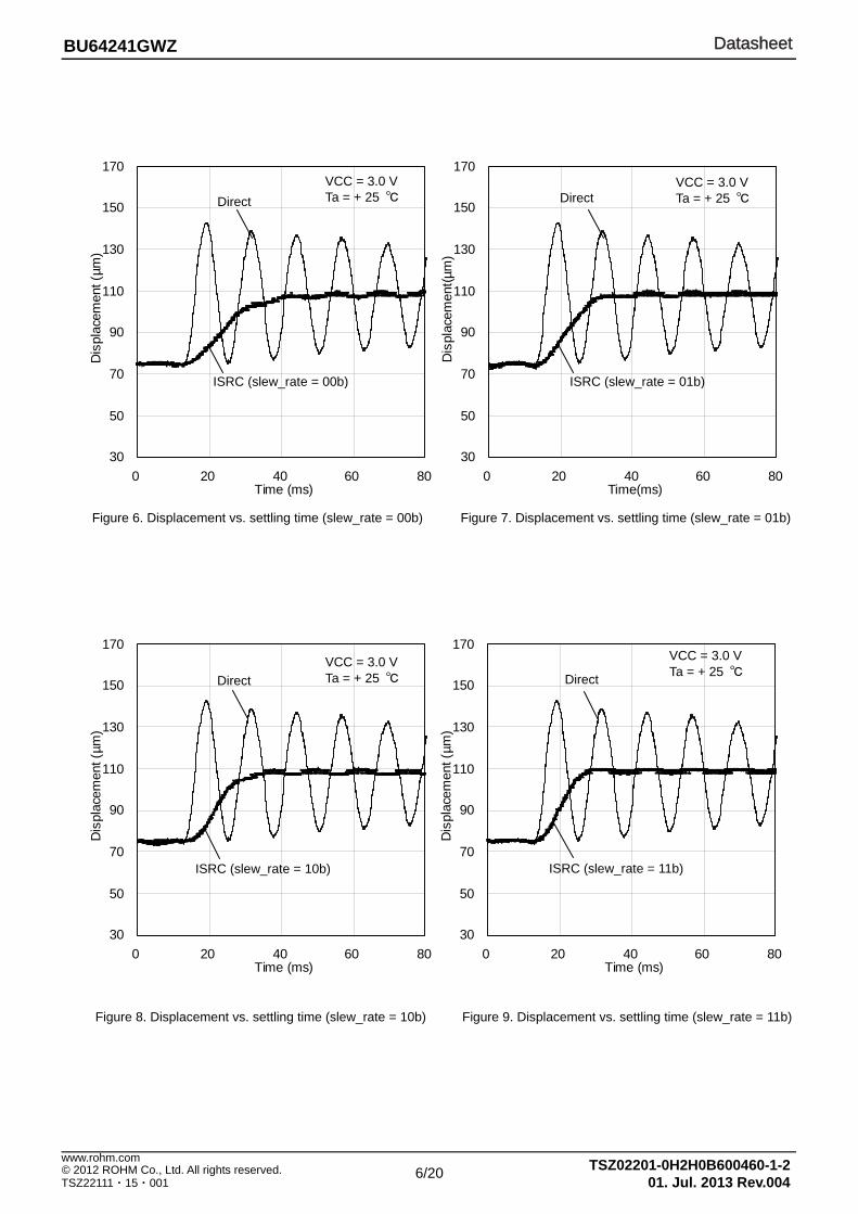
Figure 6. Displacement vs. settling time (slew_rate = 00b) Figure 7. Displacement vs. settling time (slew_rate = 01b)
Figure 8. Displacement vs. settling time (slew_rate = 10b) Figure 9. Displacement vs. settling time (slew_rate = 11b)
30
50
70
90
110
130
150
170
0 20 40 60 80Time (ms)
Dis
plac
emen
t (µm
)
30
50
70
90
110
130
150
170
0 20 40 60 80Time(ms)
Dis
plac
emen
t(µm
)30
50
70
90
110
130
150
170
0 20 40 60 80Time (ms)
Dis
plac
emen
t (µm
)
Direct
ISRC (slew_rate = 00b)
Direct
Direct Direct
ISRC (slew_rate = 01b)
ISRC (slew_rate = 10b) ISRC (slew_rate = 11b)
VCC = 3.0 V Ta = + 25
VCC = 3.0 V Ta = + 25
VCC = 3.0 V Ta = + 25
VCC = 3.0 V Ta = + 25
DatasheetDatasheet
7/20
BU64241GWZ
© 2012 ROHM Co., Ltd. All rights reserved. 01. Jul. 2013 Rev.004
www.rohm.com
TSZ22111・15・001 TSZ02201-0H2H0B600460-1-2
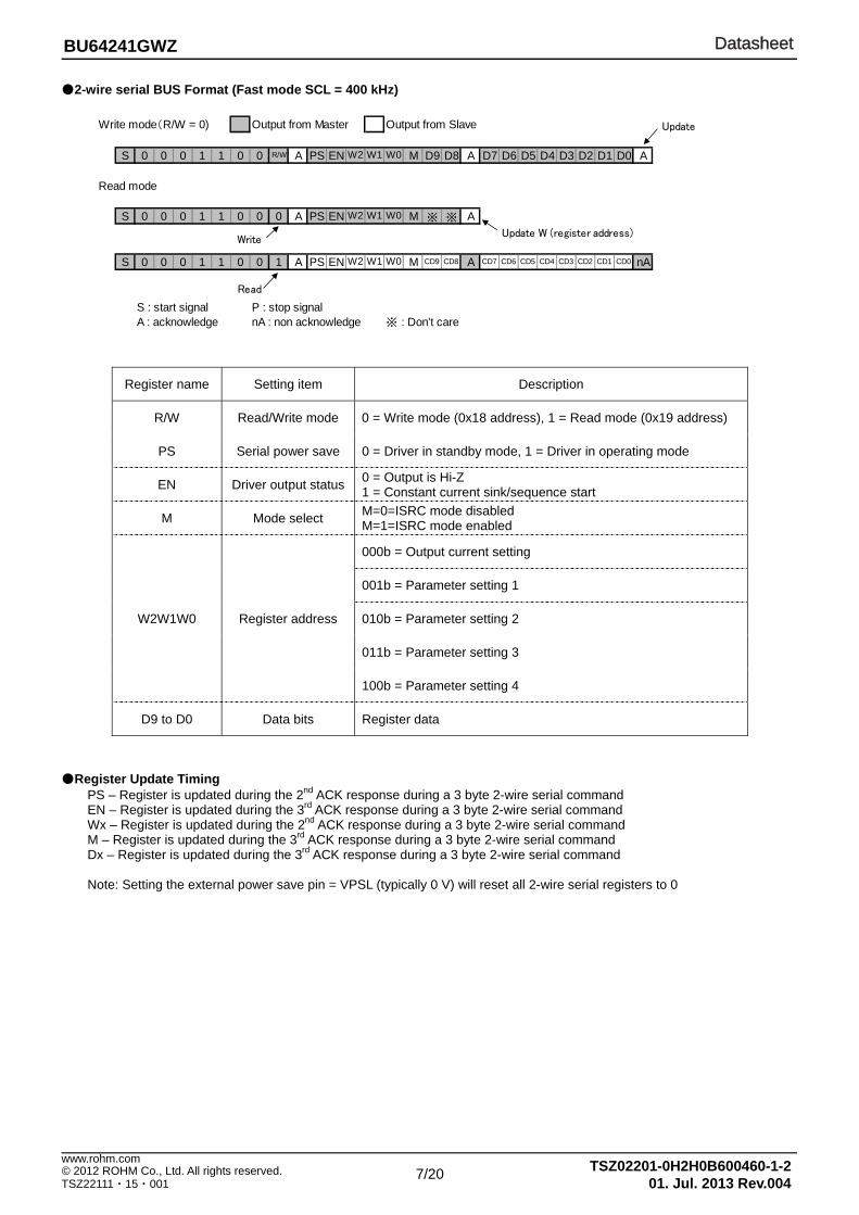
2-wire serial BUS Format (Fast mode SCL = 400 kHz)
Register Update Timing
PS – Register is updated during the 2nd ACK response during a 3 byte 2-wire serial command EN – Register is updated during the 3rd ACK response during a 3 byte 2-wire serial command Wx – Register is updated during the 2nd ACK response during a 3 byte 2-wire serial command M – Register is updated during the 3rd ACK response during a 3 byte 2-wire serial command Dx – Register is updated during the 3rd ACK response during a 3 byte 2-wire serial command Note: Setting the external power save pin = VPSL (typically 0 V) will reset all 2-wire serial registers to 0
Register name Setting item Description
R/W Read/Write mode 0 = Write mode (0x18 address), 1 = Read mode (0x19 address)
PS Serial power save 0 = Driver in standby mode, 1 = Driver in operating mode
EN Driver output status 0 = Output is Hi-Z 1 = Constant current sink/sequence start
M Mode select M=0=ISRC mode disabled M=1=ISRC mode enabled
W2W1W0 Register address
000b = Output current setting
001b = Parameter setting 1
010b = Parameter setting 2
011b = Parameter setting 3
100b = Parameter setting 4
D9 to D0 Data bits Register data
Write mode(R/W = 0) Output from Master Output from Slave
S 0 0 0 1 1 0 0 R/W A PS EN W2 W1 W0 M D9 D8 A D7 D6 D5 D4 D3 D2 D1 D0 A
Read mode
S 0 0 0 1 1 0 0 0 A PS EN W2 W1 W0 M ※ ※ A
S 0 0 0 1 1 0 0 1 A PS EN W2 W1 W0 M CD9 CD8 A CD7 CD6 CD5 CD4 CD3 CD2 CD1 CD0 nA
S : start signal P : stop signalA : acknowledge nA : non acknowledge ※ : Don't care
Update
Read
WriteUpdate W (register address)
DatasheetDatasheet
8/20
BU64241GWZ
© 2012 ROHM Co., Ltd. All rights reserved. 01. Jul. 2013 Rev.004
www.rohm.com
TSZ22111・15・001 TSZ02201-0H2H0B600460-1-2
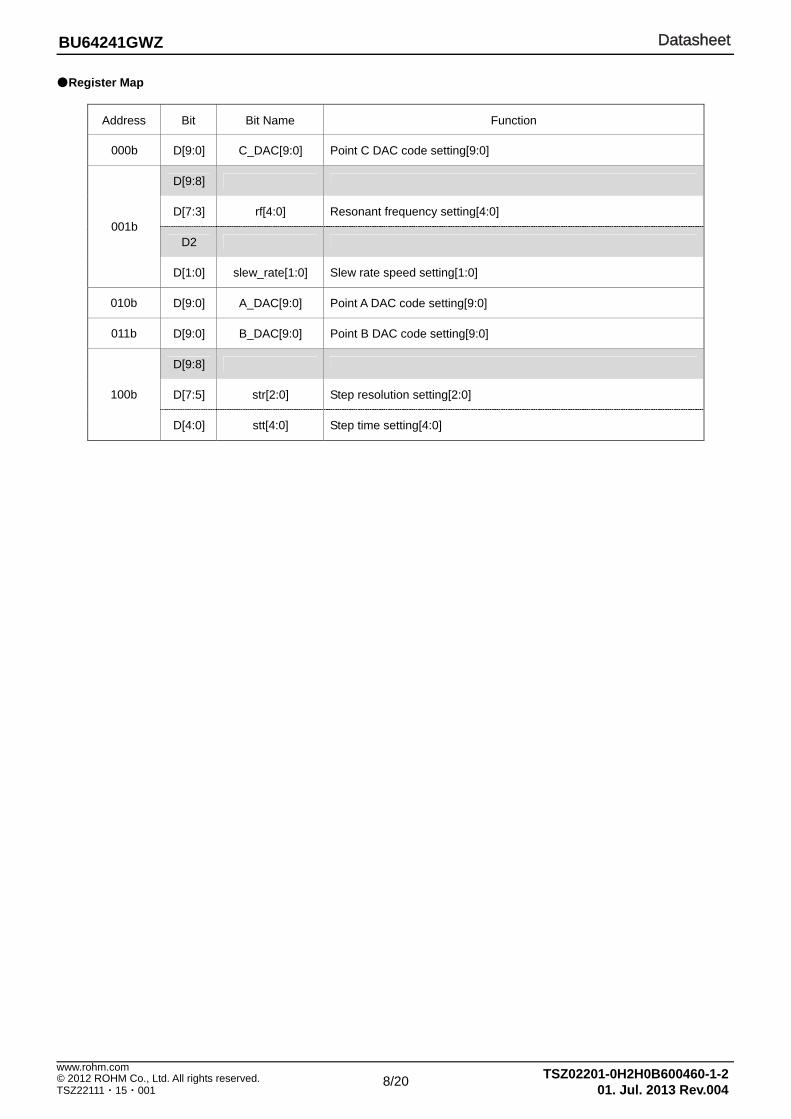
Register Map
Address Bit Bit Name Function
000b D[9:0] C_DAC[9:0] Point C DAC code setting[9:0]
001b
D[9:8]
D[7:3] rf[4:0] Resonant frequency setting[4:0]
D2
D[1:0] slew_rate[1:0] Slew rate speed setting[1:0]
010b D[9:0] A_DAC[9:0] Point A DAC code setting[9:0]
011b D[9:0] B_DAC[9:0] Point B DAC code setting[9:0]
100b
D[9:8]
D[7:5] str[2:0] Step resolution setting[2:0]
D[4:0] stt[4:0] Step time setting[4:0]
DatasheetDatasheet
9/20
BU64241GWZ
© 2012 ROHM Co., Ltd. All rights reserved. 01. Jul. 2013 Rev.004
www.rohm.com
TSZ22111・15・001 TSZ02201-0H2H0B600460-1-2
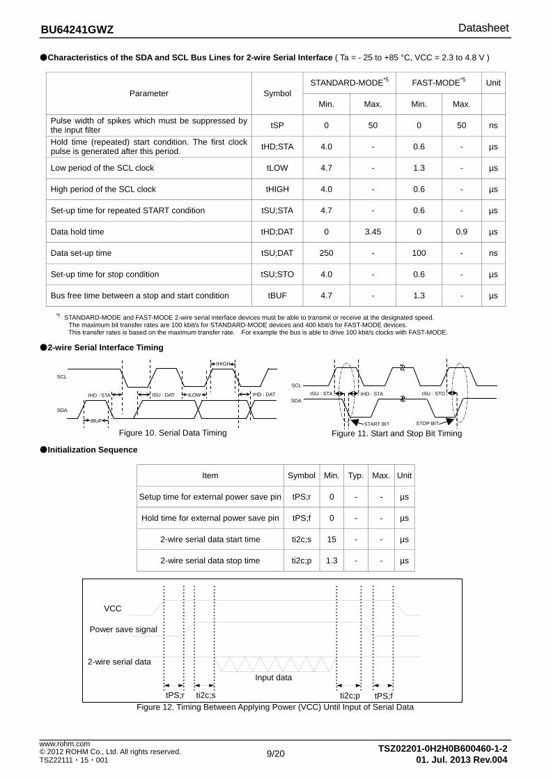
Characteristics of the SDA and SCL Bus Lines for 2-wire Serial Interface ( Ta = - 25 to +85 °C, VCC = 2.3 to 4.8 V )
Parameter Symbol STANDARD-MODE*5 FAST-MODE*5 Unit
Min. Max. Min. Max.
Pulse width of spikes which must be suppressed by the input filter tSP 0 50 0 50 ns
Hold time (repeated) start condition. The first clock pulse is generated after this period. tHD;STA 4.0 - 0.6 - µs
Low period of the SCL clock tLOW 4.7 - 1.3 - µs
High period of the SCL clock tHIGH 4.0 - 0.6 - µs
Set-up time for repeated START condition tSU;STA 4.7 - 0.6 - µs
Data hold time tHD;DAT 0 3.45 0 0.9 µs
Data set-up time tSU;DAT 250 - 100 - ns
Set-up time for stop condition tSU;STO 4.0 - 0.6 - µs
Bus free time between a stop and start condition tBUF 4.7 - 1.3 - µs
*5 STANDARD-MODE and FAST-MODE 2-wire serial interface devices must be able to transmit or receive at the designated speed. The maximum bit transfer rates are 100 kbit/s for STANDARD-MODE devices and 400 kbit/s for FAST-MODE devices. This transfer rates is based on the maximum transfer rate. For example the bus is able to drive 100 kbit/s clocks with FAST-MODE.
2-wire Serial Interface Timing Initialization Sequence
Item Symbol Min. Typ. Max. Unit
Setup time for external power save pin tPS;r 0 - - µs
Hold time for external power save pin tPS;f 0 - - µs
2-wire serial data start time ti2c;s 15 - - µs
2-wire serial data stop time ti2c;p 1.3 - - µs
SCL
tBUF
SDA
tHD : STA tSU : DAT tHD : DAT
tHIGH
tLOW
SCL
START BIT
SDA
STOP BIT
tSU : STA tHD : STA tSU : STO
Figure 10. Serial Data Timing Figure 11. Start and Stop Bit Timing
VCC
2-wire serial data
ti2c;s ti2c;p
Input data
Figure 12. Timing Between Applying Power (VCC) Until Input of Serial Data tPS;f tPS;r
Power save signal
DatasheetDatasheet
10/20
BU64241GWZ
© 2012 ROHM Co., Ltd. All rights reserved. 01. Jul. 2013 Rev.004
www.rohm.com
TSZ22111・15・001 TSZ02201-0H2H0B600460-1-2
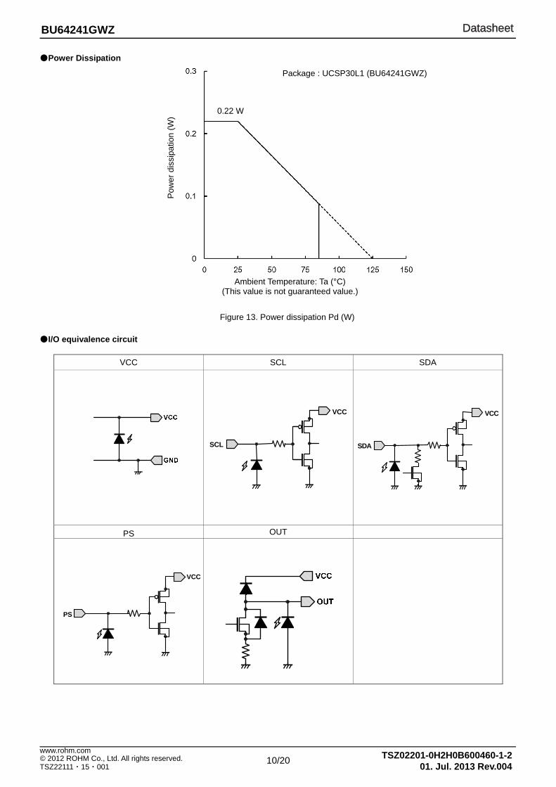
Power Dissipation
I/O equivalence circuit
VCC SCL SDA
PS OUT
Pow
er d
issi
patio
n (W
)
Ambient Temperature: Ta (°C) (This value is not guaranteed value.)
SDA
VCC
SCL
VCC
PS
VCC
0.22 W
Figure 13. Power dissipation Pd (W)
Package : UCSP30L1 (BU64241GWZ)

DatasheetDatasheet
11/20
BU64241GWZ
© 2012 ROHM Co., Ltd. All rights reserved. 01. Jul. 2013 Rev.004
www.rohm.com
TSZ22111・15・001 TSZ02201-0H2H0B600460-1-2
Controlling Mechanical Ringing A voice coil motor (VCM) is an actuator technology that is intrinsically noisy due to the properties of the mechanical spring behavior. As current passes through the VCM, the lens moves and oscillates until the system reaches a steady state. The BU64241GWZ lens driver is able to control mechanical oscillations by using the integrated ISRC (intelligent slew rate control) function. ISRC is operated by setting multiple control parameters that are determined by the intrinsic characteristics of the VCM. The following steps illustrate how to best utilize ISRC to minimize mechanical oscillations. ・Step A1 – Determining the Resonant Frequency of the VCM Each VCM has a resonant frequency that can either be provided by the manufacturer or measured. The resonant frequency of an actuator determines the amount of ringing (mechanical oscillation) experienced after the lens as been moved to a target position and the driver output current held constant. To determine the resonant frequency, f0, input a target DAC code by modifying the 10 bit C_DAC[9:0] value in register W2W1W0 = 000b that will target a final lens position approximately half of the actuator’s full stroke. Take care to not apply too much current so that the lens does not hit the mechanical end of the actuator as this will show an incorrect resonant period. In order to start movement of the lens to the DAC code that was set in C_DAC[9:0], the EN bit must be set to 1. The resonant frequency (Hz) of the actuator can be calculated with Equation 1 using the resonant period observed in Figure 14.
f0 = (T)-1
Equation1. Resonant Frequency vs. Time Period Relationship
After calculating the correct resonant frequency, program the closest value in the W2W1W0 = 001b register using the 5 bit rf[4:0] values from Table 1. When calculating the resonant frequency take care that different actuator samples’ resonant frequencies might vary slightly and that the frequency tolerance should be taken into consideration when selecting the correct driver resonant frequency value.
Table 1. f0 Settings (rf[4:0])
rf[4:0] f0 rf[4:0] f0 rf[4:0] f0 rf[4:0] f0
00000 - 01000 85 Hz 10000 125 Hz 11000 -
00001 50 Hz 01001 90 Hz 10001 130 Hz 11001 -
00010 55 Hz 01010 95 Hz 10010 135 Hz 11010 -
00011 60 Hz 01011 100 Hz 10011 140 Hz 11011 -
00100 65 Hz 01100 105 Hz 10100 145 Hz 11100 -
00101 70 Hz 01101 110 Hz 10101 150 Hz 11101 -
00110 75 Hz 01110 115 Hz 10110 - 11110 -
00111 80 Hz 01111 120 Hz 10111 - 11111 -
0
? ? ?? µm?
Time(ms)
T
Figure 14. Actuator Displacement Waveform (ISRC Disabled)
Dis
plac
emen
t (µm
)
Time (ms)
DatasheetDatasheet
12/20
BU64241GWZ
© 2012 ROHM Co., Ltd. All rights reserved. 01. Jul. 2013 Rev.004
www.rohm.com
TSZ22111・15・001 TSZ02201-0H2H0B600460-1-2
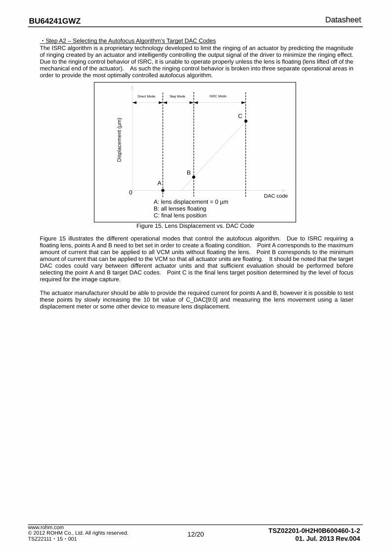
・Step A2 – Selecting the Autofocus Algorithm’s Target DAC Codes The ISRC algorithm is a proprietary technology developed to limit the ringing of an actuator by predicting the magnitude of ringing created by an actuator and intelligently controlling the output signal of the driver to minimize the ringing effect. Due to the ringing control behavior of ISRC, it is unable to operate properly unless the lens is floating (lens lifted off of the mechanical end of the actuator). As such the ringing control behavior is broken into three separate operational areas in order to provide the most optimally controlled autofocus algorithm. Figure 15 illustrates the different operational modes that control the autofocus algorithm. Due to ISRC requiring a floating lens, points A and B need to bet set in order to create a floating condition. Point A corresponds to the maximum amount of current that can be applied to all VCM units without floating the lens. Point B corresponds to the minimum amount of current that can be applied to the VCM so that all actuator units are floating. It should be noted that the target DAC codes could vary between different actuator units and that sufficient evaluation should be performed before selecting the point A and B target DAC codes. Point C is the final lens target position determined by the level of focus required for the image capture. The actuator manufacturer should be able to provide the required current for points A and B, however it is possible to test these points by slowly increasing the 10 bit value of C_DAC[9:0] and measuring the lens movement using a laser displacement meter or some other device to measure lens displacement.
Figure 15. Lens Displacement vs. DAC Code
DAC code A: lens displacement = 0 µmB: all lenses floating C: final lens position
A
B
C
0
Direct Mode Step Mode ISRC Mode
Displacement(µm)
Dis
plac
emen
t (µm
)
DatasheetDatasheet
13/20
BU64241GWZ
© 2012 ROHM Co., Ltd. All rights reserved. 01. Jul. 2013 Rev.004
www.rohm.com
TSZ22111・15・001 TSZ02201-0H2H0B600460-1-2
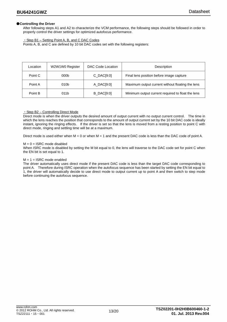
Controlling the Driver After following steps A1 and A2 to characterize the VCM performance, the following steps should be followed in order to properly control the driver settings for optimized autofocus performance. ・Step B1 – Setting Point A, B, and C DAC Codes Points A, B, and C are defined by 10 bit DAC codes set with the following registers:
Location W2W1W0 Register DAC Code Location Description
Point C 000b C_DAC[9:0] Final lens position before image capture
Point A 010b A_DAC[9:0] Maximum output current without floating the lens
Point B 011b B_DAC[9:0] Minimum output current required to float the lens
・Step B2 – Controlling Direct Mode Direct mode is when the driver outputs the desired amount of output current with no output current control. The time in which the lens reaches the position that corresponds to the amount of output current set by the 10 bit DAC code is ideally instant, ignoring the ringing effects. If the driver is set so that the lens is moved from a resting position to point C with direct mode, ringing and settling time will be at a maximum. Direct mode is used either when M = 0 or when M = 1 and the present DAC code is less than the DAC code of point A. M = 0 = ISRC mode disabled When ISRC mode is disabled by setting the M bit equal to 0, the lens will traverse to the DAC code set for point C when the EN bit is set equal to 1. M = 1 = ISRC mode enabled The driver automatically uses direct mode if the present DAC code is less than the target DAC code corresponding to point A. Therefore during ISRC operation when the autofocus sequence has been started by setting the EN bit equal to 1, the driver will automatically decide to use direct mode to output current up to point A and then switch to step mode before continuing the autofocus sequence.
DatasheetDatasheet
14/20
BU64241GWZ
© 2012 ROHM Co., Ltd. All rights reserved. 01. Jul. 2013 Rev.004
www.rohm.com
TSZ22111・15・001 TSZ02201-0H2H0B600460-1-2
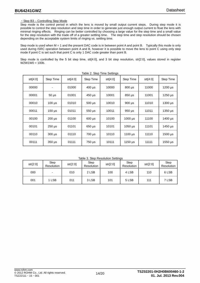
・Step B3 – Controlling Step Mode Step mode is the control period in which the lens is moved by small output current steps. During step mode it is possible to control the step resolution and step time in order to generate just enough output current to float the lens with minimal ringing effects. Ringing can be better controlled by choosing a large value for the step time and a small value for the step resolution with the trade off of a greater settling time. The step time and step resolution should be chosen depending on the acceptable system limits of ringing vs. settling time. Step mode is used when M = 1 and the present DAC code is in between point A and point B. Typically this mode is only used during ISRC operation between point A and B, however it is possible to move the lens to point C using only step mode if point C is set such that point C is only 1 DAC code greater than point B. Step mode is controlled by the 5 bit step time, stt[4:0], and 3 bit step resolution, str[2:0], values stored in register W2W1W0 = 100b.
Table 2. Step Time Settings
stt[4:0] Step Time stt[4:0] Step Time stt[4:0] Step Time stt[4:0] Step Time
00000 - 01000 400 µs 10000 800 µs 11000 1200 µs
00001 50 µs 01001 450 µs 10001 850 µs 11001 1250 µs
00010 100 µs 01010 500 µs 10010 900 µs 11010 1300 µs
00011 150 µs 01011 550 µs 10011 950 µs 11011 1350 µs
00100 200 µs 01100 600 µs 10100 1000 µs 11100 1400 µs
00101 250 µs 01101 650 µs 10101 1050 µs 11101 1450 µs
00110 300 µs 01110 700 µs 10110 1100 µs 11110 1500 µs
00111 350 µs 01111 750 µs 10111 1150 µs 11111 1550 µs
Table 3. Step Resolution Settings
str[2:0] Step Resolution str[2:0] Step
Resolution str[2:0] Step Resolution str[2:0] Step
Resolution
000 - 010 2 LSB 100 4 LSB 110 6 LSB
001 1 LSB 011 3 LSB 101 5 LSB 111 7 LSB

DatasheetDatasheet
15/20
BU64241GWZ
© 2012 ROHM Co., Ltd. All rights reserved. 01. Jul. 2013 Rev.004
www.rohm.com
TSZ22111・15・001 TSZ02201-0H2H0B600460-1-2
・Step B4 – Controlling ISRC Mode ISRC mode is the control period in which the lens is already floating and the driver smoothly moves the lens based on the proprietary behavior of the ISRC algorithm. ISRC operation keeps ringing at a minimum while achieving the fastest possible settling time based on the ISRC operational conditions.
ISRC mode is used when M = 1 and the present DAC code is greater than the DAC code for point B. If the target DAC code for point C is set so that the value is too large and will cause excess ringing, the point C DAC code is automatically updated with a driver pre-determined value to minimize the ringing effect. When M = 1, the driver will automatically switch between direct mode, step mode, and ISRC mode when the point A, B, and C DAC code conditions are met. The condition for this automatic transitioning to occur is when the register values for point A, point B, point C, step time, and step resolution are all set to values other than 0 and then the sequence will start when the EN bit is set equal to 1.
Figure 16. Three Modes Sequential Operation (Shown as DAC Codes)
Figure 17. Three Modes Sequential Operation (Shown as Lens Displacement)
0Time (ms)
ISRC DAC codes*
Start sequence
B
A
C
Step mode
Direct mode
ISRC mode* ISRC DAC codes the details of ISRC operation are proprietary
DA
C c
ode
0
Sequence start point
Dis
plac
emen
t (µm
)
Time (ms)
DatasheetDatasheet
16/20
BU64241GWZ
© 2012 ROHM Co., Ltd. All rights reserved. 01. Jul. 2013 Rev.004
www.rohm.com
TSZ22111・15・001 TSZ02201-0H2H0B600460-1-2
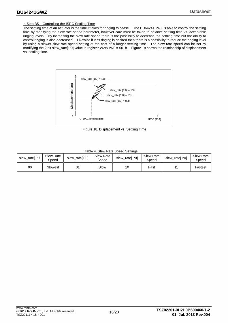
・Step B5 – Controlling the ISRC Settling Time The settling time of an actuator is the time it takes for ringing to cease. The BU64241GWZ is able to control the settling time by modifying the slew rate speed parameter, however care must be taken to balance settling time vs. acceptable ringing levels. By increasing the slew rate speed there is the possibility to decrease the settling time but the ability to control ringing is also decreased. Likewise if less ringing is desired then there is a possibility to reduce the ringing level by using a slower slew rate speed setting at the cost of a longer settling time. The slew rate speed can be set by modifying the 2 bit slew_rate[1:0] value in register W2W1W0 = 001b. Figure 18 shows the relationship of displacement vs. settling time.
Table 4. Slew Rate Speed Settings
slew_rate[1:0] Slew Rate Speed slew_rate[1:0] Slew Rate
Speed slew_rate[1:0] Slew Rate Speed slew_rate[1:0] Slew Rate
Speed
00 Slowest 01 Slow 10 Fast 11 Fastest
Figure 18. Displacement vs. Settling Time
0
移動量〔um〕
Time〔ms〕
Slew_rate〔1:0〕=2'b00
Slew_rate〔1:0〕=2'b01
Slew_rate〔1:0〕=2'b10
Slew_rate〔1:0〕=2'b11
T_DAC〔9:0〕変更
Dis
plac
emen
t (µm
)
Time (ms)C_DAC [9:0] update
slew_rate [1:0] = 11b
slew_rate [1:0] = 10b
slew_rate [1:0] = 01b
slew_rate [1:0] = 00b
DatasheetDatasheet
17/20
BU64241GWZ
© 2012 ROHM Co., Ltd. All rights reserved. 01. Jul. 2013 Rev.004
www.rohm.com
TSZ22111・15・001 TSZ02201-0H2H0B600460-1-2
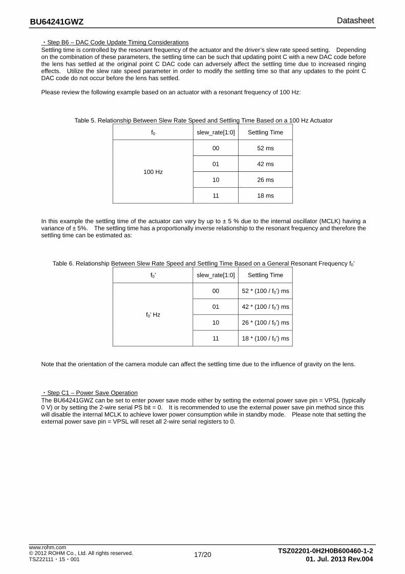
・Step B6 – DAC Code Update Timing Considerations Settling time is controlled by the resonant frequency of the actuator and the driver’s slew rate speed setting. Depending on the combination of these parameters, the settling time can be such that updating point C with a new DAC code before the lens has settled at the original point C DAC code can adversely affect the settling time due to increased ringing effects. Utilize the slew rate speed parameter in order to modify the settling time so that any updates to the point C DAC code do not occur before the lens has settled. Please review the following example based on an actuator with a resonant frequency of 100 Hz:
Table 5. Relationship Between Slew Rate Speed and Settling Time Based on a 100 Hz Actuator
f0 slew_rate[1:0] Settling Time
100 Hz
00 52 ms
01 42 ms
10 26 ms
11 18 ms
In this example the settling time of the actuator can vary by up to ± 5 % due to the internal oscillator (MCLK) having a variance of ± 5%. The settling time has a proportionally inverse relationship to the resonant frequency and therefore the settling time can be estimated as:
Table 6. Relationship Between Slew Rate Speed and Settling Time Based on a General Resonant Frequency f0’
f0’ slew_rate[1:0] Settling Time
f0’ Hz
00 52 * (100 / f0’) ms
01 42 * (100 / f0’) ms
10 26 * (100 / f0’) ms
11 18 * (100 / f0’) ms
Note that the orientation of the camera module can affect the settling time due to the influence of gravity on the lens.
・Step C1 – Power Save Operation The BU64241GWZ can be set to enter power save mode either by setting the external power save pin = VPSL (typically 0 V) or by setting the 2-wire serial PS bit = 0. It is recommended to use the external power save pin method since this will disable the internal MCLK to achieve lower power consumption while in standby mode. Please note that setting the external power save pin = VPSL will reset all 2-wire serial registers to 0.
DatasheetDatasheet
18/20
BU64241GWZ
© 2012 ROHM Co., Ltd. All rights reserved. 01. Jul. 2013 Rev.004
www.rohm.com
TSZ22111・15・001 TSZ02201-0H2H0B600460-1-2
Operational Notes (1) Absolute maximum ratings
Use of the IC in excess of absolute maximum ratings such as the applied voltage or operating temperature range (Topr) may result in IC damage. Assumptions should not be made regarding the state of the IC (short mode or open mode) when such damage is incurred. The implementation of a physical safety measure such as a fuse should be considered when there is use of the IC in a special mode where it’s anticipated that the absolute maximum ratings may be exceeded.
(2) Power supply lines Regenerated current may flow as a result of the motor's back electromotive force. Insert capacitors between the power supply and ground pins to serve as a route for regenerated current. Determine the capacitance based on of all the characteristics of an electrolytic capacitor due to the electrolytic capacitor possibly losing some capacitance at low temperatures. If the connected power supply does not have sufficient current absorption capacity, regenerative current will cause the voltage on the power supply line to rise, which combined with the product and its peripheral circuitry may exceed the absolute maximum ratings. It is recommended to implement a physical safety measure such as the insertion of a voltage clamp diode between the power supply and GND pins.
(3) Heat dissipation Use a thermal design that allows for a sufficient margin regarding the power dissipation (Pd) during actual operating conditions.
(4) Use in strong magnetic fields Use caution when using the IC in the presence of a strong magnetic field as doing so may cause the IC to malfunction.
(5) ASO When using the IC, set the output transistor for the motor so that it does not exceed absolute maximum ratings or ASO.
(6) Thermal shutdown circuit This IC incorporates a TSD (thermal shutdown) circuit. If the temperature of the chip reaches the below temperature, the motor coil output will be opened. The thermal shutdown circuit (TSD circuit) is designed only to shut off the IC to prevent runaway thermal operation. It is not designed to protect the IC or to guarantee its operation. Do not continue to use the IC after use of the TSD feature or use the IC in an environment where the its assumed that the TSD feature will be used.
TSD ON temperature [°C] (Typ.)
Hysteresis temperature [°C] (Typ.)
150 20
(7) Ground Wiring Pattern Ensure a minimum GND pin potential in all operating conditions. When using GND patterns for both small signal and large currents, it is recommended to isolate the two ground patterns by placing a single ground point at the application's reference point. This will help to alleviate noise in the small signal ground voltage due to noise created by the ground pattern wiring resistance for large current blocks. Be careful not to change the GND wiring pattern of any external components.
(8) Power Save (PS) terminal
PS holds the reset function on logic concurrently. Please release PS after the start-up of VCC. Reset is not normally done when VCC is short-circuited to PS and it uses it, and there is a possibility of malfunctions.

DatasheetDatasheet
19/20
BU64241GWZ
© 2012 ROHM Co., Ltd. All rights reserved. 01. Jul. 2013 Rev.004
www.rohm.com
TSZ22111・15・001 TSZ02201-0H2H0B600460-1-2
Ordering Part Number
B U 6 4 2 4 1 G W Z E2
Part Number
Package GWZ: UCSP30L1
Packaging and forming specification E2: Embossed tape and reel
Physical Dimension Tape and Reel Information
Marking Diagram(TOP VIEW)
Tape Embossed carrier tape
Quantity 6,000 pcs / reel
Direction of feed E2 (See neighboring image)
ReelDirection of feed1pin
1234 1234 1234 1234 1234 1234
<Packing specification>
1PIN MARK
ABX
Lot No.
Product Name
UCSP30L1 (BU64241GWZ)
UCSP30L1 (BU64241GWZ)
*Order quantity needs to be multiple of the minimum quantity.
3
0.1
85×
0.0
56-φ0.20±0.05
1.30±0.03
2
B
S
1
AA0.05
0.06
B
0.25±0.05
B
0.7
7±0.
03
S0.06
A
1PIN MARK
P=0.4×2
0.33M
AX
0.4
BX
Lot No.
BX
Product Name
Lot No. 1PIN MARK
(Unit: mm)

DatasheetDatasheet
20/20
BU64241GWZ
© 2012 ROHM Co., Ltd. All rights reserved. 01. Jul. 2013 Rev.004
www.rohm.com
TSZ22111・15・001 TSZ02201-0H2H0B600460-1-2
Revision History
Date Revision Changes
15.Oct.2012 001 New Release
11.Apr.2013 002 Add information about “BU64243GWZ”.
31.May.2013 003 Delete information about “BU64240GWZ”.
01.Jul.2013 004 Delete information about “BU64243GWZ”.

DatasheetDatasheet
Notice - GE Rev.002© 2014 ROHM Co., Ltd. All rights reserved.
Notice Precaution on using ROHM Products
1. Our Products are designed and manufactured for application in ordinary electronic equipments (such as AV equipment, OA equipment, telecommunication equipment, home electronic appliances, amusement equipment, etc.). If you intend to use our Products in devices requiring extremely high reliability (such as medical equipment (Note 1), transport equipment, traffic equipment, aircraft/spacecraft, nuclear power controllers, fuel controllers, car equipment including car accessories, safety devices, etc.) and whose malfunction or failure may cause loss of human life, bodily injury or serious damage to property (“Specific Applications”), please consult with the ROHM sales representative in advance. Unless otherwise agreed in writing by ROHM in advance, ROHM shall not be in any way responsible or liable for any damages, expenses or losses incurred by you or third parties arising from the use of any ROHM’s Products for Specific Applications.
(Note1) Medical Equipment Classification of the Specific Applications JAPAN USA EU CHINA
CLASSⅢ CLASSⅢ
CLASSⅡb CLASSⅢ
CLASSⅣ CLASSⅢ
2. ROHM designs and manufactures its Products subject to strict quality control system. However, semiconductor
products can fail or malfunction at a certain rate. Please be sure to implement, at your own responsibilities, adequate safety measures including but not limited to fail-safe design against the physical injury, damage to any property, which a failure or malfunction of our Products may cause. The following are examples of safety measures:
[a] Installation of protection circuits or other protective devices to improve system safety [b] Installation of redundant circuits to reduce the impact of single or multiple circuit failure
3. Our Products are designed and manufactured for use under standard conditions and not under any special or extraordinary environments or conditions, as exemplified below. Accordingly, ROHM shall not be in any way responsible or liable for any damages, expenses or losses arising from the use of any ROHM’s Products under any special or extraordinary environments or conditions. If you intend to use our Products under any special or extraordinary environments or conditions (as exemplified below), your independent verification and confirmation of product performance, reliability, etc, prior to use, must be necessary:
[a] Use of our Products in any types of liquid, including water, oils, chemicals, and organic solvents [b] Use of our Products outdoors or in places where the Products are exposed to direct sunlight or dust [c] Use of our Products in places where the Products are exposed to sea wind or corrosive gases, including Cl2,
H2S, NH3, SO2, and NO2
[d] Use of our Products in places where the Products are exposed to static electricity or electromagnetic waves [e] Use of our Products in proximity to heat-producing components, plastic cords, or other flammable items [f] Sealing or coating our Products with resin or other coating materials [g] Use of our Products without cleaning residue of flux (even if you use no-clean type fluxes, cleaning residue of
flux is recommended); or Washing our Products by using water or water-soluble cleaning agents for cleaning residue after soldering
[h] Use of the Products in places subject to dew condensation
4. The Products are not subject to radiation-proof design. 5. Please verify and confirm characteristics of the final or mounted products in using the Products. 6. In particular, if a transient load (a large amount of load applied in a short period of time, such as pulse. is applied,
confirmation of performance characteristics after on-board mounting is strongly recommended. Avoid applying power exceeding normal rated power; exceeding the power rating under steady-state loading condition may negatively affect product performance and reliability.
7. De-rate Power Dissipation (Pd) depending on Ambient temperature (Ta). When used in sealed area, confirm the actual
ambient temperature. 8. Confirm that operation temperature is within the specified range described in the product specification. 9. ROHM shall not be in any way responsible or liable for failure induced under deviant condition from what is defined in
this document.
Precaution for Mounting / Circuit board design 1. When a highly active halogenous (chlorine, bromine, etc.) flux is used, the residue of flux may negatively affect product
performance and reliability. 2. In principle, the reflow soldering method must be used; if flow soldering method is preferred, please consult with the
ROHM representative in advance. For details, please refer to ROHM Mounting specification

DatasheetDatasheet
Notice - GE Rev.002© 2014 ROHM Co., Ltd. All rights reserved.
Precautions Regarding Application Examples and External Circuits 1. If change is made to the constant of an external circuit, please allow a sufficient margin considering variations of the
characteristics of the Products and external components, including transient characteristics, as well as static characteristics.
2. You agree that application notes, reference designs, and associated data and information contained in this document
are presented only as guidance for Products use. Therefore, in case you use such information, you are solely responsible for it and you must exercise your own independent verification and judgment in the use of such information contained in this document. ROHM shall not be in any way responsible or liable for any damages, expenses or losses incurred by you or third parties arising from the use of such information.
Precaution for Electrostatic
This Product is electrostatic sensitive product, which may be damaged due to electrostatic discharge. Please take proper caution in your manufacturing process and storage so that voltage exceeding the Products maximum rating will not be applied to Products. Please take special care under dry condition (e.g. Grounding of human body / equipment / solder iron, isolation from charged objects, setting of Ionizer, friction prevention and temperature / humidity control).
Precaution for Storage / Transportation 1. Product performance and soldered connections may deteriorate if the Products are stored in the places where:
[a] the Products are exposed to sea winds or corrosive gases, including Cl2, H2S, NH3, SO2, and NO2 [b] the temperature or humidity exceeds those recommended by ROHM [c] the Products are exposed to direct sunshine or condensation [d] the Products are exposed to high Electrostatic
2. Even under ROHM recommended storage condition, solderability of products out of recommended storage time period may be degraded. It is strongly recommended to confirm solderability before using Products of which storage time is exceeding the recommended storage time period.
3. Store / transport cartons in the correct direction, which is indicated on a carton with a symbol. Otherwise bent leads
may occur due to excessive stress applied when dropping of a carton. 4. Use Products within the specified time after opening a humidity barrier bag. Baking is required before using Products of
which storage time is exceeding the recommended storage time period.
Precaution for Product Label QR code printed on ROHM Products label is for ROHM’s internal use only.
Precaution for Disposition When disposing Products please dispose them properly using an authorized industry waste company.
Precaution for Foreign Exchange and Foreign Trade act Since our Products might fall under controlled goods prescribed by the applicable foreign exchange and foreign trade act, please consult with ROHM representative in case of export.
Precaution Regarding Intellectual Property Rights 1. All information and data including but not limited to application example contained in this document is for reference
only. ROHM does not warrant that foregoing information or data will not infringe any intellectual property rights or any other rights of any third party regarding such information or data. ROHM shall not be in any way responsible or liable for infringement of any intellectual property rights or other damages arising from use of such information or data.:
2. No license, expressly or implied, is granted hereby under any intellectual property rights or other rights of ROHM or any
third parties with respect to the information contained in this document.
Other Precaution 1. This document may not be reprinted or reproduced, in whole or in part, without prior written consent of ROHM. 2. The Products may not be disassembled, converted, modified, reproduced or otherwise changed without prior written
consent of ROHM. 3. In no event shall you use in any way whatsoever the Products and the related technical information contained in the
Products or this document for any military purposes, including but not limited to, the development of mass-destruction weapons.
4. The proper names of companies or products described in this document are trademarks or registered trademarks of
ROHM, its affiliated companies or third parties.
DatasheetDatasheet
Notice – WE Rev.001© 2014 ROHM Co., Ltd. All rights reserved.
General Precaution 1. Before you use our Pro ducts, you are requested to care fully read this document and fully understand its contents.
ROHM shall n ot be in an y way responsible or liabl e for fa ilure, malfunction or acci dent arising from the use of a ny ROHM’s Products against warning, caution or note contained in this document.
2. All information contained in this docume nt is current as of the issuing date and subj ect to change without any prior
notice. Before purchasing or using ROHM’s Products, please confirm the la test information with a ROHM sale s representative.
3. The information contained in this doc ument is provi ded on an “as is” basis and ROHM does not warrant that all
information contained in this document is accurate an d/or error-free. ROHM shall not be in an y way responsible or liable for any damages, expenses or losses incurred by you or third parties resulting from inaccuracy or errors of or concerning such information.