linear integrated circuits - datasheet4u.com filelinear integrated circuits 3-terminal positive...
TRANSCRIPT
LINEAR INTEGRATED CIRCUITS
3-TERMINAL POSITIVE VOLTAGE REGULATORS
• OUTPUT CURRENT UP TO 1.5A • OUTPUT VOLTAGES OF 5; 6; 8; 12; 15; 18; 20; 24V • THERMAL OVERLOAD PROTECTION • SHORT CIRCUIT PROTECTION • OUTPUT TRANSISTOR SOA PROTECTION
The L7800 series of three-terminal positive regulators is available in TO-220 and TO-3 packages and with several fixed output voltages, making it useful in a wide range of applications. These regulators can provide local on-card regulation, eliminating the distribution problems associated with single point regulation. Each type employs internal current limiting, thermal shut-down and safe area protection, making it essentially indestructible. If adequate heat sinking is provided, they can deliver over 1 A output current. Although designed primarily as fixed voltage regulators, these devices can be used with external components to obtain adjustable voltages and currents.
ABSOLUTE MAXIMUM RATINGS
Vi DC input voltage (for Va = 5 to 18V) (for Va = 20, 24V)
Output current Power dissipation Operating junction temperature (for L7800)
(for L7800C) Storage temperature
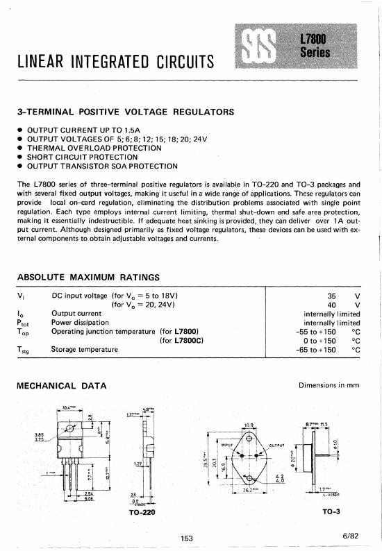
MECHANICAL DATA
TO-220
153
35 40
V V
internally limited internally limited
-55 to +150 °C Oto+150 °C
-65 to + 150°C
Dimensions in mm
8.,....,1.7
(.-00$3It
TO-3
6/82
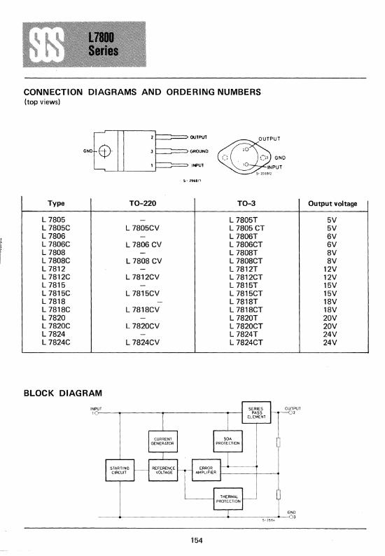
CONNECTION DIAGRAMS AND ORDERING NUMBERS (top views)
~o OUTPUT
C). ~")3 GND
,0 INPUT 5--25&912
!)-lSti8/'
Type TO-220 TO-3
L 7805 - L 7805T L 7805C L 7805CV L 7805 CT L 7806 - L 7806T L 7806C L 7806 CV L 7806CT L 7808 - L 7808T L 7808C L 7808 CV L 7808CT L 7812 - L 7812T L 7812C L 7812CV L 7812CT L 7815 - L 7815T L 7815C L 7815CV L 7815CT L 7818 - L 7818T L 7818C L 7818CV L 7818CT L 7820 - L 7820T L 7820C L 7820CV L 7820CT L 7824 - L 7824T L 7824C L 7824CV L 7824CT
BLOCK DIAGRAM
INPut 'O---~--------~-------------~-1
154
Output voltage
5V 5V 6V 6V 8V 8V
12V 12V 15V 15V 18V 18V 20V 20V 24V 24V
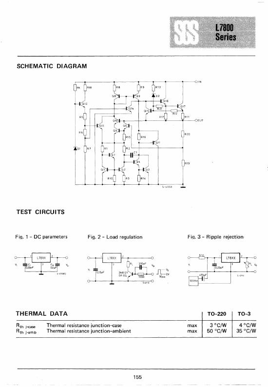
SCHEMATIC DIAGRAM
R5
R6
R15
D1 R7 R, R2
07
TEST CIRCUITS
Fi!l. 1 - DC parameters Fig. 2 - Load regulation
THERMAL DATA
Rth H:ase Rth j-amb
Thermal resistance junction-case Thermal resistance junction-ambient
155
R12
Qll
Q17
Rll OUT
R20
R19
Fi!l. 3 - Ripple rejection I
max max
TO-220
3°C/W 50°C/W
TO-3
4°C/W 35°C/W
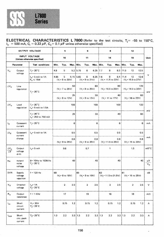
ELECTRICAL CHARACTERISTICS L 7800 (Refer to the test circuits, TJ= -55 to 150"C, 10 = 500 rnA, Ci = 0.33 iJ.F, Co = 0.1 iJ.F unless otherwise specified)
OUTPUT VOLTAGE 5 6 8 12
INPUT VOLTAGE 10 11 14 19 Unit (Unless otherwise specified)
Parameter Test conditions Min. Typ. Max. Min. Typ. Max. Min. Typ. Max. Min. Typ. Max.
Vo Output Tj: 25°C 4.8 5 5.2 5.75 6 6.25 7.7 8 8.3 11.5 12 12.5 voltage
V lo""5mAto1A 4.65 5 5.15 5.65 6 6.35 7.6 8 8.4 11.4 12 12.6 Po ,,15W (V,: 8 to 20V) (V,: 9 to 21V) (V,: 11.5 to 23V) (V,: 15.5t027V)
tNo Line 50 60 80 120 regulation (V,: 7 to 25V) (V,: 8 to 25V) (V,: 10.5 to 25V) (V,: 14.5t030V)
Tj: 25°C mV 25 30 40 60
(V,: 8 to 12V) (V,: 9 to 13V) (V,: 11 to 17V) (V,: l&to 22V)
t1Vo Load Tj: 25°C 100 100 100 120 regulation 10:5mAtol.5A
mV Tj: 25°C 25 30 40 60 10= 250 to 750 rnA
'd Quiescent Tj: 25°C 6 6 6 6 mA current
t1'd Quiescent lo=5rnAto 1A 0.5 0.5 0.5 0.5 current change 0.8 0.8 0.8 0.8
mA
(Vi: 8 to 25V) (V,: 9 to 25V) (V,: 11.5 to 25V) (V,: 15 to 30V)
t1Vo Output 10= 5 rnA 0.6 0.7 1 1.5 mV/oC
TT voltage drift
eN output B: 10Hz to 100KHz 40 40 40 40 ",V noise Tj: 25°C voltage
--Vo
SVR Supply f: 120Hz 68 65 62 61 dB voltage (V,: 8 to 18V) (V,: 9 to 19V) (V,: 11.5 to 21.5V) (V,: 15 to 25V) rejection
Vd Dropout 10= 1A 2 2.5 2 2.5 2 2.5 2 2.5 V voltage T): 25°C
Ro Output f: 1 KHz 17 19 16 18 mil resistance
'se Short Vi: 35V 0.75 1.2 0.75 1.2 0.75 1.2 0.75 1.2 A circuit T): 25°C current
Iscp Short Tj: 25°C 1.3 2.2 3.3 1.3 2.2 3.3 1.3 2.2 3.3 1.3 2.2 3.3 A eire. peak
cuP'"ent
156
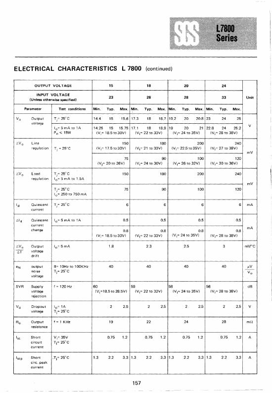
ELECTRICAL CHARACTERISTICS L 7800 (continued)
OUTPUT VOLTAGE 15 18 20 24
INPUT VOLTAGE 23 26
(Unless otherwise specified) 28 33 Unit
Parameter Test conditions Min. Typ. Max. Min. Typ. Max. Min. Typ. Max. Min. Typ. Max.
Va Output TJ= 25'C 14.4 15 15.6 17.3 18 18.7 19.2 20 20.8 23 24 25 voltage
V '0"" 5 mA to 1 A 14.25 15 15.75 17.1 18 18.9 19 20 21 22.8 24 25.2 Po';;;; l5W IV;= 18.5 to 30VI IV;= 22 to 33VI IV;= 24 to 35VI IV;= 28 to 38VI
:o.Va Line 150 180 200 240 regulation TJ = 25'C IV;= 17.5 to 30VI IV;= 21 to 33VI IV;= 22.5 to 35VI IV;= 27 to 38VI
rnV
75 90 100 120 IVj= 20 to 26VI IV;= 24 to 30VI IV;= 26 to 32VI IV;= 30 to 36VI
6.V a Load TJ= 25'C 150 180 200 240 regulation 10= 5 mA to 1.5A
rnV
Tj = 25°C 75 90 100 120
'0= 250 to 750 mA
Id Quiescent Tj= 25'C 6 6 6 6 rnA current
6. l d Quiescent 'o==5mAtolA 0.5 0.5 0.5 0.5 current change rnA
0.8 0.8 0.8 0.8 IV;= 18.5to30VI IV;= 22 to 33VI IV;= 24 to 35VI IV;= 28 to 38VI
6.Va Output 10= 5 mA 1.8 2.3 2.5 3 rnV/oC
c;:T voltage drift
eN output B= 10Hz to 100KHz 40 40 40 40 ~V
nOIse Tj= 25°C --
Va voltage
SVR Supply f = 120 Hz 60 59 58 56 dB voltage IV;=18.5 to 28.5VI IV;= 22 to 32VI IV;= 24 to 35VI IV;= 28 to 38VI rejection
Vd Dropout 10= lA 2 2.5 2 2.5 2 2.5 2 2.5 V voltage Tj'= 2SoC
Ra Output f = 1 KHz 19 22 24 28 rnD resistance
I" Shart V;= 35V 0.75 1.2 0.75 1.2 0.75 1.2 0.75 1.2 A circuit Tj= 25°C current
tscp Short .Tj = 25°C 1.3 2.2 3.3 1.3 2.2 3.3 1.3 2.2 3.3 1.3 2.2 3.3 A eire. peak current
157
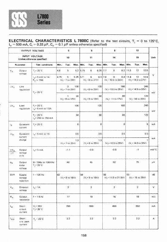
ELECTRICAL CHARACTERISTICS L 7800C (Refer to the test circuits, Tj
10 = 500 mA, Cj = 0.33 JlF, Co = 0.1 JlF unless otherwise specified) o to 125°C,
OUTPUT VOLTAGE 5 6 8 12
INPUT VOLTAGE 10 11 14 19 Unit
(Unless otherwise specified)
Parameter Test conditions Min. Typ. Max. Min. Typ. Max. Min. Typ. Max. Min. Typ. Max.
Vo Output TJ= 25'C 4.S 5 5.2 5.75 6 6.25 7.7 S S.3 11.5 12 12.5
voltage V
lo""5mAtolA 4.75 5 5.25 5.7 6 6.3 7.6 S S.4 11.4 12 12.6
Po";; 15W (V i= 7 to 20VI (V j "" 8 to 21 V) (V i= 10.5 to 25VI (V i= 14.5 to 27VI
:c,V o Line 3 100 120 160 240
regulation (V i= 7 to 25VI (V i= S to 25VI (V i=10.5t025VI (V i= 14.5to30VI TJ= 25'C mV
1 50 60 SO 120
(V i= S to 12VI (V i= 9 to 13VI (V i= 11 to 17VI (V i= 16 to 22VI
~Vo Load T j = 25'C 100 120 160 240
regulation 10= 5 mA to 1.5A mV
T j = 25'C 50 60 SO 120
10= 250 to 750 mA
Id Quiescent T j = 25'C S 8 8 S rnA
current
L.ld Quiescent lo=5mAtolA 0.5 0.5 0.5 0.5
current
change rnA
1.3 1.3 1 1 (Vi= 7 to 25Vj (Vj= 8 to 25V) (V i= 10.5 to 25VI (V i= 14.5to30VI
-~ Output 10= 5 rnA -1.1 -O.S -O.S -1 mV/'C
6T voltage
drift
eN Output B'" 10Hz to 100KHz 40 45 52 75 MV
noise TJc 25'C voltage
SVR Supply f=120Hz 62 59 56 55 dB
voltage (V i= S to lSVI (V i= 9 to 19VI (V i= 11.5 to 21.5V) (V i= 15 to 25VI
rejection
Vd Dropout 10= lA 2 2 2 2 V
voltage
Ro Output f = 1 KHz 17 19 16 18 mil
resistance
I,c Short Vi= 35V 750 550 450 350 rnA
circuit T j = 25'C
current
Iscp Short T j = 25'C 2.2 2.2 2.2 2.2 A eire. peak current
158
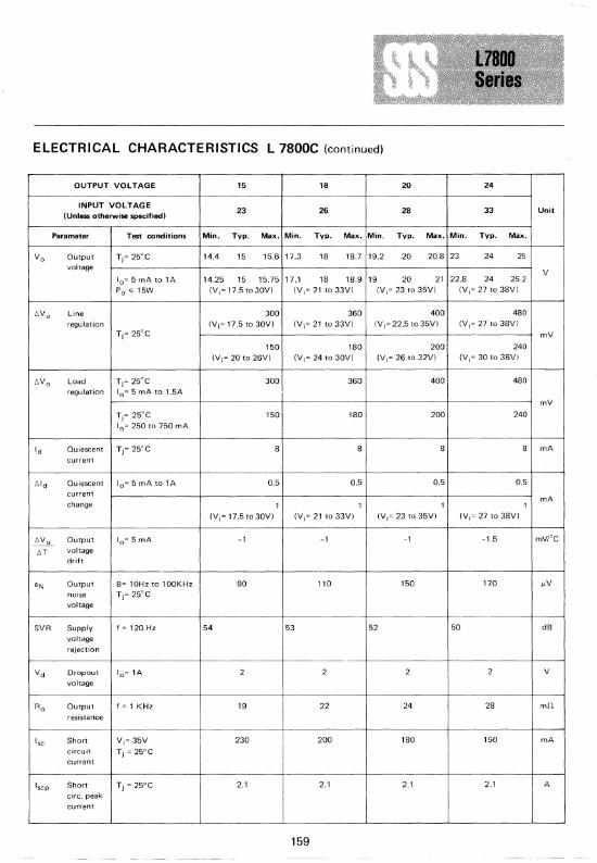
ELECTRICAL CHARACTERISTICS L 7800C (continued)
OUTPUT VOLTAGE 15 18 20 24
INPUT VOLTAGE 23 26 33
(Unless otherwise specified) 28 Unit
Parameter Test conditions Min. Typ. Max. Min. Typ. Max. Min. Typ. Max. Min. Typ. Max.
Va Output Tj " 25°C 14.4 15 15.6 17.3 18 18.7 19.2 20 20.8 23 24 25
voltage V
lo""5mAto lA 14.25 15 15.75 17.1 18 18.9 19 20 21 22.8 24 25.2
Po';;;; 15W IV;" 17.5 to 30VI IV;" 21 to 33VI IV;" 23 to 35VI IV;" 27 to 38VI
"Va Line 300 360 400 480
regulation IV;" 17.5 to 30VI IV;" 21 to 33VI IV;" 22.5 to 35VI IV;" 27 to 38VI TJ" 25°C rnV
150 180 200 240
IV;" 20 to 26VI IV;" 24 to 30VI IV;" 26 to 32VI IV;" 30 to 36VI
"Va Load TJ" 25°C 300 360 400 480
regulation r a '" 5 rnA to 1 .5A rnV
T j " 25°C 150 180 200 240
10 ::' 250 to 750 rnA
Id Quiescent T j " 25°C 8 8 8 8 rnA
current
"Id Quiescent lo=5mAto lA 0.5 0.5 0.5 0.5
current
change rnA
1 1 1 1
IV;" 17.5t030VI IV;" 21 to 33VI IV;" 23 to 35VI IV;" 27 to 38VI
~ Output 10= 5 rnA -1 -1 -1 -1.5 rnV/oC
"T voltage
drift
eN Output B= 10Hz to 100KHz 90 110 150 170 ~V
noise T j " 25c C voltage
SVR Supply f"120Hz 54 53 52 50 dB
voltage rejection
Vd Dropout 10= 1A 2 2 2 i 2 V
voltage
Ro Output f = 1 KHz 19 22 24 28 rnn
resistance
-
Iso Short Vi'" 35V 230 200 180 150 rnA
circuit T j "25°C current
Isep Short Tj ~ 25°C 2.1 2.1 2.1 2.1 A
eire. peak
current
159
IV'
'.5
05
''Ie (V)
~ ,
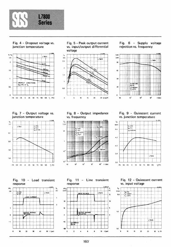
Fig. 4 - Dropout voltage vs. junction temperature
L 78XX
i""-r--i""- t---~ -... -...: :::-.. t---- J",.
r-::: ::--~ t-- 20~ ---~ f- DROPOUT CONDITIONS
AVo:OSo,. of Vo
-75 -50 -25 0 25 50 75 100 125, Tj re)
Fig. 7 - Output voltage vs. junction temperature
-75 -50 -25 0 25 50 75 100 125 Tj (oe)
Fig. 10 - Load transient response
G 2971
rlv I I r-I L 7805
r- %= v
-+t= LOAD CURREN
i I, , I
.1-.
i ,
I OUTPUT VOLTAGE I"-DEVIATON
V I , ! I
r--H~ I
I
10 20 50 t (us)
(0
(AI
(0
(A,
2.5
1.5
0.5
Fig. 5 - Peak output current vs. input/output differential voltage
Fig. 8 - Output impedance vs. freauency
20 'lfll'!l (11) ~
10
0
10'
Fig. 11 response
10' 10'
Line transient
G-291211 .v (m' I
, v, v, (
INPUT VOlTAGE I L7805 15
i I ..i I
20 (Q
I
I 10
~~mTo~TAGEI ,
I I Io-SOOmA I i 'SV
~1O
~20 ~ I o 10 t{JJs)
160
Fig. 6 - Supplv voltage rejection vs. frequency
::rTTlmTi,~~'TImII~TITI!m-Tlrll'~i1i~ eo • i II'! III +t+l,++i'#--'--"80-"-5 +ti+llI
till II F ' I '1111 I
60 rr--t.ljjjjH-lr++I+8---i-m, +1I-+Htflill
40 ,II ! . --4 '. ..~ 111 ~.
20 :Jltiil ~t:""",_t.idI8 .. v-Hlt-t+tttt1lt--+++ti+llI . 1,IIil ~;"'C"
'd (rnA)
4.2
4.0
3.8
3.6
Hili 1I11 10 10' )()' f (Hz)
Fig. 9 - Quiescent current vs. junction temperature
G-297"
H;;;): I I I I : . +-f-mtt' H +~++
%1 --+-/ i I I
/ I ! •
I---. -+tt-t i L780S
, l I I I I -15 -50 -25 0 2S 50 75 100 125 Tj (Oe)
Fig. 12 - Quiescent current vs. input voltage
10 20 25 30 Vi (V)
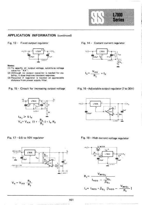
APPLICATION INFORMATION (continued)
Fig. 13 - Fixed output regulator
Notes: (1) To specify an output voltage, substitute voltage
value for "XX". (2) Although no output capacitor is needed for sta
bility, it does improve transient response. (3) Required if regulator is located an appreciable
distance from power supply filter.
Fig. 15 - Circuit for increasing output voltage
vxx! R1
R2
Fi~. 17 - 0.5 to 10V regulator
161
Fig. 14 - Costant current regulator
V;
IFig. 16 -Adjustable output regulator (7 to 30V)
Fig. 18 - HiQh current voltage regulator
VBEQ1
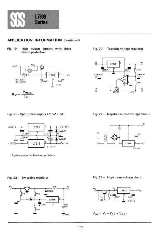
APPLICATION INFORMATION (continued)
Fig. 19 - High output current with short circuit protection
Fig. 21 - Split power supply (±15V - 1A)
+20VC)--'---'-I F--~>---'-O + 15 V
- 20Vo--""'--"l r--4-...... -o·15V·
• Against potential latch-up problems
Fig. 23 - Switching regulator
162
Fig. 20 - Tracking voltage regulator
'\10
COMMON
~
-Vo
Fig. 22 - Negative output voltage circuit
JI
Fig. 24 - High input voltage circuit
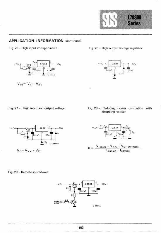
APPLICATION INFORMATION (continued)
Fig. 25 - High input voltage circuit
Fig. 27 - High input and output voltage
Fig. 29 - Remote shuntdown
163
Fig. 26 - High output voltage regu lator
Fig. 28 - Reducing power dissipation with dropping resistor
R = ~mjn) - Vxx - VOROP(max)
lo(max) + Id(max)
APPLICATION INFORMATION (continued)
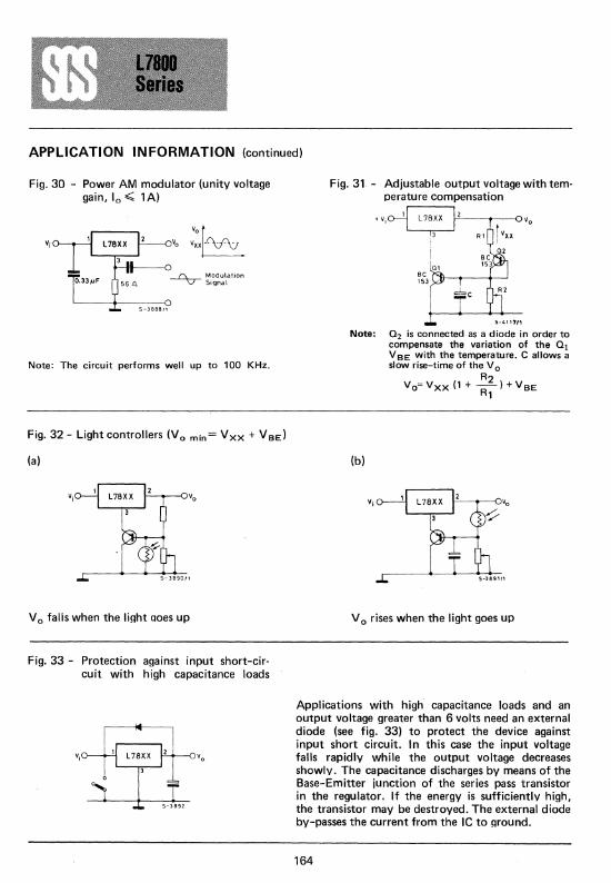
Fig. 30 - Power AM modulator (unity voltage gain, 10 ';;; 1A)
Note: The circuit performs well up to 100 KHz.
Fig. 32 - Light controllers (Vo min= Vxx + VBE )
(a)
v 0 falls when the Ii!lht !loes up
Fig. 33 - Protection against input short-circuit with high capacitance loads
Fig. 31 - Adjustable output voltage with temperature compensation
. v;o-!j L 7BXX Ir'---t----< 13 !
Q1
~~3 C&-r--t---'
5-4117"
Note: 02 is connected as a diode in order to compensate the variation of the 01 V BE with the temperature. C allows a slow rise-time of the V 0
(b)
V;
R2 Vo= Vxx (1 + --I +VBE
R1
Vo rises when the light goes up
Applications with high capacitance loads and an output voltage greater than 6 volts need an external diode (see fig. 33) to protect the device against input short circuit. In this case the input voltage falls rapidly while the output voltage decreases showly. The capacitance discharges by means of the Base-Emitter junction of the series pass transistor in the regulator. If the energy is sufficiently high, the transistor may be destroyed. The external diode by-passes the current from the Ie to !lround.
164