little bits of diamond: optically detected magnetic...
TRANSCRIPT

Little bits of diamond: Optically detected magnetic resonance of nitrogen-vacancycentersHaimei Zhang, Carina Belvin, Wanyi Li, Jennifer Wang, Julia Wainwright, Robbie Berg, and Joshua Bridger
Citation: American Journal of Physics 86, 225 (2018); doi: 10.1119/1.5023389View online: https://doi.org/10.1119/1.5023389View Table of Contents: http://aapt.scitation.org/toc/ajp/86/3Published by the American Association of Physics Teachers
Articles you may be interested inA compact disc under skimming light raysAmerican Journal of Physics 86, 169 (2018); 10.1119/1.5021904
Can mechanical energy vanish into thin air?American Journal of Physics 86, 220 (2018); 10.1119/1.5019022
A study of kinetic friction: The Timoshenko oscillatorAmerican Journal of Physics 86, 174 (2018); 10.1119/1.5008862
Gravitational waves from orbiting binaries without general relativityAmerican Journal of Physics 86, 186 (2018); 10.1119/1.5020984
Twelve years before the quantum no-cloning theoremAmerican Journal of Physics 86, 201 (2018); 10.1119/1.5021356
Heat transfer and evaporative cooling in the function of pot-in-pot coolersAmerican Journal of Physics 86, 206 (2018); 10.1119/1.5016041

APPARATUS AND DEMONSTRATION NOTESThe downloaded PDF for any Note in this section contains all the Notes in this section.
John Essick, EditorDepartment of Physics, Reed College, Portland, OR 97202
This department welcomes brief communications reporting new demonstrations, laboratory equip-ment, techniques, or materials of interest to teachers of physics. Notes on new applications of olderapparatus, measurements supplementing data supplied by manufacturers, information which, while notnew, is not generally known, procurement information, and news about apparatus under developmentmay be suitable for publication in this section. Neither the American Journal of Physics nor the Editorsassume responsibility for the correctness of the information presented.
Manuscripts should be submitted using the web-based system that can be accessed via the AmericanJournal of Physics home page, http://ajp.dickinson.edu and will be forwarded to the ADN editor forconsideration.
Little bits of diamond: Optically detected magnetic resonanceof nitrogen-vacancy centers
Haimei Zhang, Carina Belvin,a) Wanyi Li,b) Jennifer Wang, Julia Wainwright,and Robbie Bergc)
Department of Physics, Wellesley College, Wellesley, Massachusetts 02481
Joshua BridgerDover Sherborn High School, Dover, Massachusetts 02030
(Received 1 August 2017; accepted 18 January 2018)
We give instructions for the construction and operation of a simple apparatus for performing
optically detected magnetic resonance measurements on diamond samples containing high
concentrations of nitrogen-vacancy (NV) centers. Each NV center has a spin degree of freedom
that can be manipulated and monitored by a combination of visible and microwave radiation. We
observe Zeeman shifts in the presence of small external magnetic fields and describe a simple
method to optically measure magnetic field strengths with a spatial resolution of several microns.
The activities described are suitable for use in an advanced undergraduate lab course, powerfully
connecting core quantum concepts to cutting edge applications. An even simpler setup, appropriate
for use in more introductory settings, is also presented. VC 2018 American Association of Physics Teachers.
https://doi.org/10.1119/1.5023389
I. INTRODUCTION
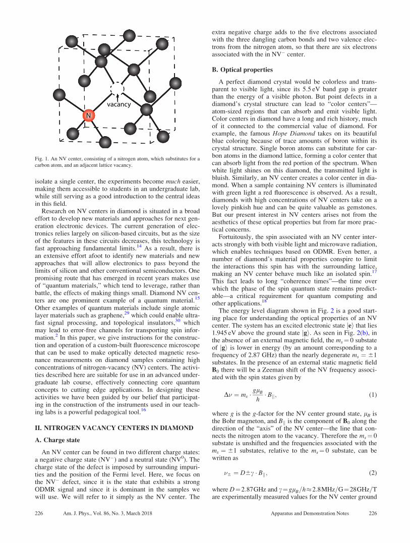
Magnetic resonance spectroscopy is a technique of greatpower and scope. As a result, magnetic resonance experimentsare a common and valuable addition to an advanced under-graduate physics laboratory.1,2 Here, we describe a series ofmagnetic resonance experiments where we transfer the detec-tion of the magnetic interactions to the optical domain, greatlyincreasing the detection efficiency. The increased sensitivityof this optically detected magnetic resonance (ODMR) mark-edly simplifies the experiments, allowing students to buildmuch of the setup from scratch. As an added benefit, the sys-tem that we study, the nitrogen vacancy (NV) point defect indiamond, has attracted wide attention for its potential applica-tion in quantum computing and magnetic sensing applications.As shown in Fig. 1, an NV center consists of one substitu-tional nitrogen defect and an adjacent vacancy. The electronsthat comprise this system are contributed by the nitrogenimpurity and the dangling bonds from the carbon atoms thatsurround the vacancy. Collectively, these electrons possess anet spin of one unit of angular momentum, which can bemanipulated and monitored in an ODMR experiment.
To appreciate the power of ODMR, consider this: In a con-ventional magnetic resonance experiment the signal generated
by a single spin is ridiculously small, so, of necessity, experi-ments are performed on large ensembles of spins. For exam-ple, a modern NMR spectrometer typically has a minimumsample volume of �10 ll, corresponding to �1017 (in thiscase, nuclear) spins.3 It is therefore quite remarkable that, inrecent years, ODMR experiments routinely control and detectthe electronic spin state of individual NV centers.4–7 This 17orders of magnitude improvement in sensitivity is not onlyamazing, but also of great practical interest, since single spinscan serve as quantum bits (qubits) for quantum computingapplications8 or as atom-sized classical bits for memory stor-age.9 They can also be used to measure a number of physicalquantities, such as magnetic field10,11 and temperature,12 withnanometer spatial resolution.
While ODMR experiments that manipulate the spin of asingle NV center have become commonplace in researchlabs around the world, these experiments are challenging,since they require isolating the fluorescence from a singlecenter. This is typically accomplished with a custom confo-cal microscope, which is expensive, complicated, andrequires highly precise alignment.13 Such an instrument isclearly out of scale for our pedagogical purposes here.Instead we describe ODMR measurements that are made onlarge ensembles of NV centers. By relaxing the need to
225 Am. J. Phys. 86 (3), March 2018 http://aapt.org/ajp VC 2018 American Association of Physics Teachers 225
isolate a single center, the experiments become much easier,making them accessible to students in an undergraduate lab,while still serving as a good introduction to the central ideasin this field.
Research on NV centers in diamond is situated in a broadeffort to develop new materials and approaches for next gen-eration electronic devices. The current generation of elec-tronics relies largely on silicon-based circuits, but as the sizeof the features in these circuits decreases, this technology isfast approaching fundamental limits.14 As a result, there isan extensive effort afoot to identify new materials and newapproaches that will allow electronics to pass beyond thelimits of silicon and other conventional semiconductors. Onepromising route that has emerged in recent years makes useof “quantum materials,” which tend to leverage, rather thanbattle, the effects of making things small. Diamond NV cen-ters are one prominent example of a quantum material.15
Other examples of quantum materials include single atomiclayer materials such as graphene,29 which could enable ultra-fast signal processing, and topological insulators,30 whichmay lead to error-free channels for transporting spin infor-mation.2 In this paper, we give instructions for the construc-tion and operation of a custom-built fluorescence microscopethat can be used to make optically detected magnetic reso-nance measurements on diamond samples containing highconcentrations of nitrogen-vacancy (NV) centers. The activi-ties described here are suitable for use in an advanced under-graduate lab course, effectively connecting core quantumconcepts to cutting edge applications. In designing theseactivities we have been guided by our belief that participat-ing in the construction of the instruments used in our teach-ing labs is a powerful pedagogical tool.16
II. NITROGEN VACANCY CENTERS IN DIAMOND
A. Charge state
An NV center can be found in two different charge states:a negative charge state (NV�) and a neutral state (NV0). Thecharge state of the defect is imposed by surrounding impuri-ties and the position of the Fermi level. Here, we focus onthe NV� defect, since it is the state that exhibits a strongODMR signal and since it is dominant in the samples wewill use. We will refer to it simply as the NV center. The
extra negative charge adds to the five electrons associatedwith the three dangling carbon bonds and two valence elec-trons from the nitrogen atom, so that there are six electronsassociated with the in NV� center.
B. Optical properties
A perfect diamond crystal would be colorless and trans-parent to visible light, since its 5:5 eV band gap is greaterthan the energy of a visible photon. But point defects in adiamond’s crystal structure can lead to “color centers”—atom-sized regions that can absorb and emit visible light.Color centers in diamond have a long and rich history, muchof it connected to the commercial value of diamond. Forexample, the famous Hope Diamond takes on its beautifulblue coloring because of trace amounts of boron within itscrystal structure. Single boron atoms can substitute for car-bon atoms in the diamond lattice, forming a color center thatcan absorb light from the red portion of the spectrum. Whenwhite light shines on this diamond, the transmitted light isbluish. Similarly, an NV center creates a color center in dia-mond. When a sample containing NV centers is illuminatedwith green light a red fluorescence is observed. As a result,diamonds with high concentrations of NV centers take on alovely pinkish hue and can be quite valuable as gemstones.But our present interest in NV centers arises not from theaesthetics of these optical properties but from far more prac-tical concerns.
Fortuitously, the spin associated with an NV center inter-acts strongly with both visible light and microwave radiation,which enables techniques based on ODMR. Even better, anumber of diamond’s material properties conspire to limitthe interactions this spin has with the surrounding lattice,making an NV center behave much like an isolated spin.17
This fact leads to long “coherence times”—the time overwhich the phase of the spin quantum state remains predict-able—a critical requirement for quantum computing andother applications.18
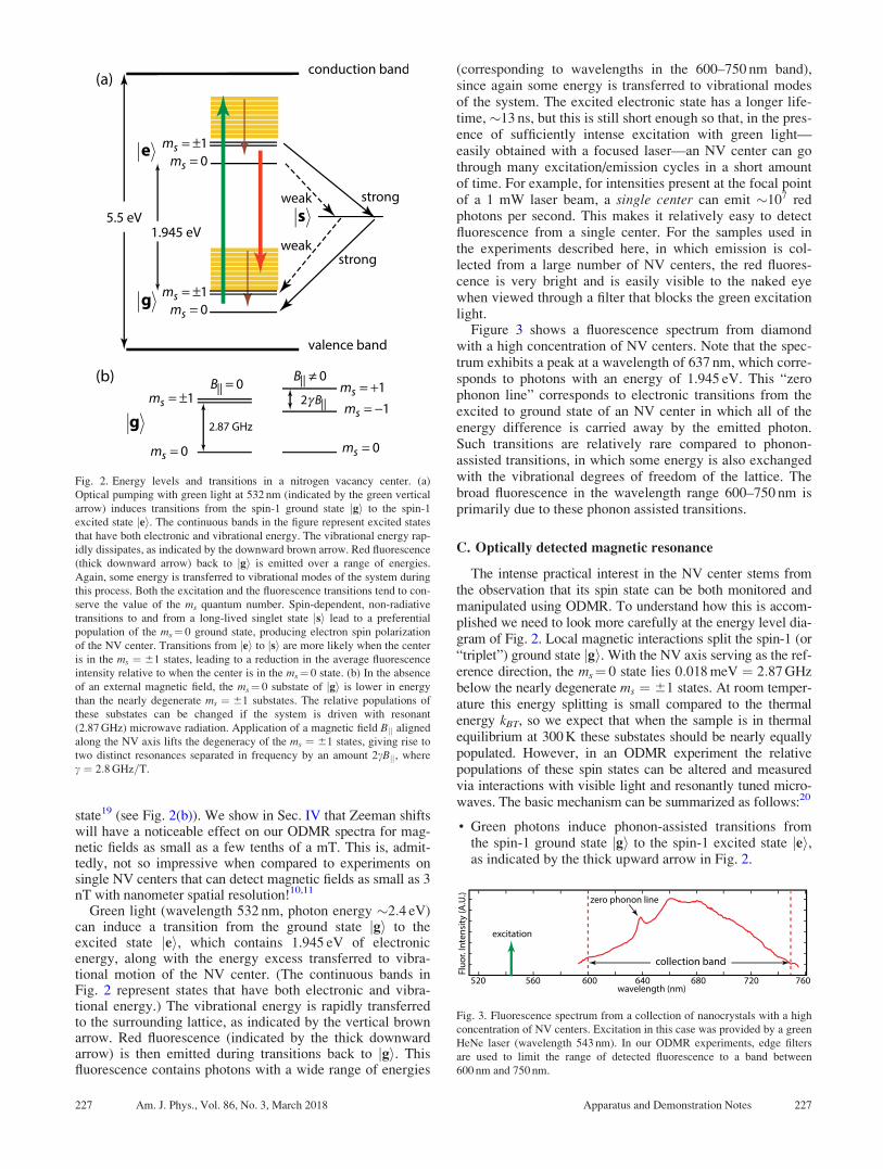
The energy level diagram shown in Fig. 2 is a good start-ing place for understanding the optical properties of an NVcenter. The system has an excited electronic state jei that lies1.945 eV above the ground state jgi. As seen in Fig. 2(b), inthe absence of an external magnetic field, the ms¼ 0 substateof jgi is lower in energy (by an amount corresponding to afrequency of 2.87 GHz) than the nearly degenerate ms ¼ 61substates. In the presence of an external static magnetic fieldB0 there will be a Zeeman shift of the NV frequency associ-ated with the spin states given by
D� ¼ ms �glB
h� Bjj; (1)
where g is the g-factor for the NV center ground state, lB isthe Bohr magneton, and Bjj is the component of B0 along thedirection of the “axis” of the NV center—the line that con-nects the nitrogen atom to the vacancy. Therefore the ms¼ 0substate is unshifted and the frequencies associated with thems ¼ 61 substates, relative to the ms¼ 0 substate, can bewritten as
�6 ¼ D6c � Bjj; (2)
where D¼2:87GHz and c¼glB=h�2:8MHz=G¼28GHz=Tare experimentally measured values for the NV center ground
Fig. 1. An NV center, consisting of a nitrogen atom, which substitutes for a
carbon atom, and an adjacent lattice vacancy.
226 Am. J. Phys., Vol. 86, No. 3, March 2018 Apparatus and Demonstration Notes 226
state19 (see Fig. 2(b)). We show in Sec. IV that Zeeman shiftswill have a noticeable effect on our ODMR spectra for mag-netic fields as small as a few tenths of a mT. This is, admit-tedly, not so impressive when compared to experiments onsingle NV centers that can detect magnetic fields as small as 3nT with nanometer spatial resolution!10,11
Green light (wavelength 532 nm, photon energy �2:4 eV)can induce a transition from the ground state jgi to theexcited state jei, which contains 1.945 eV of electronicenergy, along with the energy excess transferred to vibra-tional motion of the NV center. (The continuous bands inFig. 2 represent states that have both electronic and vibra-tional energy.) The vibrational energy is rapidly transferredto the surrounding lattice, as indicated by the vertical brownarrow. Red fluorescence (indicated by the thick downwardarrow) is then emitted during transitions back to jgi. Thisfluorescence contains photons with a wide range of energies
(corresponding to wavelengths in the 600–750 nm band),since again some energy is transferred to vibrational modesof the system. The excited electronic state has a longer life-time, �13 ns, but this is still short enough so that, in the pres-ence of sufficiently intense excitation with green light—easily obtained with a focused laser—an NV center can gothrough many excitation/emission cycles in a short amountof time. For example, for intensities present at the focal pointof a 1 mW laser beam, a single center can emit �107 redphotons per second. This makes it relatively easy to detectfluorescence from a single center. For the samples used inthe experiments described here, in which emission is col-lected from a large number of NV centers, the red fluores-cence is very bright and is easily visible to the naked eyewhen viewed through a filter that blocks the green excitationlight.
Figure 3 shows a fluorescence spectrum from diamondwith a high concentration of NV centers. Note that the spec-trum exhibits a peak at a wavelength of 637 nm, which corre-sponds to photons with an energy of 1.945 eV. This “zerophonon line” corresponds to electronic transitions from theexcited to ground state of an NV center in which all of theenergy difference is carried away by the emitted photon.Such transitions are relatively rare compared to phonon-assisted transitions, in which some energy is also exchangedwith the vibrational degrees of freedom of the lattice. Thebroad fluorescence in the wavelength range 600–750 nm isprimarily due to these phonon assisted transitions.
C. Optically detected magnetic resonance
The intense practical interest in the NV center stems fromthe observation that its spin state can be both monitored andmanipulated using ODMR. To understand how this is accom-plished we need to look more carefully at the energy level dia-gram of Fig. 2. Local magnetic interactions split the spin-1 (or“triplet”) ground state jgi. With the NV axis serving as the ref-erence direction, the ms¼ 0 state lies 0:018 meV ¼ 2:87 GHzbelow the nearly degenerate ms ¼ 61 states. At room temper-ature this energy splitting is small compared to the thermalenergy kBT, so we expect that when the sample is in thermalequilibrium at 300 K these substates should be nearly equallypopulated. However, in an ODMR experiment the relativepopulations of these spin states can be altered and measuredvia interactions with visible light and resonantly tuned micro-waves. The basic mechanism can be summarized as follows:20
• Green photons induce phonon-assisted transitions fromthe spin-1 ground state jgi to the spin-1 excited state jei,as indicated by the thick upward arrow in Fig. 2.
Fig. 2. Energy levels and transitions in a nitrogen vacancy center. (a)
Optical pumping with green light at 532 nm (indicated by the green vertical
arrow) induces transitions from the spin-1 ground state jgi to the spin-1
excited state jei. The continuous bands in the figure represent excited states
that have both electronic and vibrational energy. The vibrational energy rap-
idly dissipates, as indicated by the downward brown arrow. Red fluorescence
(thick downward arrow) back to jgi is emitted over a range of energies.
Again, some energy is transferred to vibrational modes of the system during
this process. Both the excitation and the fluorescence transitions tend to con-
serve the value of the ms quantum number. Spin-dependent, non-radiative
transitions to and from a long-lived singlet state jsi lead to a preferential
population of the ms¼ 0 ground state, producing electron spin polarization
of the NV center. Transitions from jei to jsi are more likely when the center
is in the ms ¼ 61 states, leading to a reduction in the average fluorescence
intensity relative to when the center is in the ms¼ 0 state. (b) In the absence
of an external magnetic field, the ms¼ 0 substate of jgi is lower in energy
than the nearly degenerate ms ¼ 61 substates. The relative populations of
these substates can be changed if the system is driven with resonant
(2.87 GHz) microwave radiation. Application of a magnetic field Bjj aligned
along the NV axis lifts the degeneracy of the ms ¼ 61 states, giving rise to
two distinct resonances separated in frequency by an amount 2cBjj, where
c ¼ 2:8 GHz=T.
Fig. 3. Fluorescence spectrum from a collection of nanocrystals with a high
concentration of NV centers. Excitation in this case was provided by a green
HeNe laser (wavelength 543 nm). In our ODMR experiments, edge filters
are used to limit the range of detected fluorescence to a band between
600 nm and 750 nm.
227 Am. J. Phys., Vol. 86, No. 3, March 2018 Apparatus and Demonstration Notes 227

• Phonon-assisted fluorescence due to transitions back to jgiis detected in 600–750 nm range. These optical transitionsare indicated by the thick downward arrow in Fig. 2.
• The optical transitions described in the above bullet pointstend to preserve spin orientation. (That is, the value of ms
is typically not altered during these transitions.)• There also exists a long-lived spin-0 (singlet) state jsi that
can only be accessed via non-radiative transitions. Theselection rules associated with these non-radiative transi-tions are such that illumination with green laser light leadsto a preferential population of the ms¼ 0 ground state.
• Transitions from jei to jsi are more likely when the centeris in a ms ¼ 61 state relative to when it is in a ms¼ 0state. So a center in a ms ¼ 61 state ends up spending asignificant fraction of time “stuck” in the jsi state, leadingto a reduction in the average fluorescence intensity relativeto when the center is in the ms¼ 0 state.
The upshot is that when illuminated with green light, thereexists an optical pumping mechanism that tends to drive theNV center into the ms¼ 0 substate. Also, when an NV centeris in a ms ¼ 61 substate the intensity of the red fluorescencewill be noticeably less than when it is in the ms¼ 0 substate.
The relative populations of the ms¼ 0 and ms ¼ 61 sub-states can be changed if the system is driven with resonantmicrowave radiation. In a typical ODMR measurement, thesample is illuminated with green light and the intensity ofthe red fluorescence is monitored as an applied microwavefield is slowly tuned into resonance. At resonance there willbe an easily detectable reduction of fluorescence intensity.
III. EXPERIMENTAL METHODS
A. Samples
We made measurements on diamond crystals of three dif-ferent size scales: large single crystals (�1� 5 mm across),microcrystals (�10� 20 lm across), and nanocrystals(�100 nm across). In all three cases, the samples have highconcentrations of NV centers, so when we recorded ODMRspectra large ensembles of NV centers were being measuredat once.
Large single crystal diamond. Large single crystal dia-mond samples (lateral dimensions up to �5 mm) with a highconcentration of NV centers were provided to us by our col-laborators at Element Six, a leading commercial producer ofsynthetic diamonds. Diamond single crystals were synthe-sized at high pressures and high temperatures. These samplestypically have an optically smooth [111] surface. As grown,these crystals contained relatively high concentrations of iso-lated nitrogen impurities (� 100 ppm), resulting in color cen-ters that gave them a yellowish-brown hue. Samples werethen irradiated with 4.5 MeV electrons (dose2� 1018e=cm2), administered over the course of 2 h, whichcreated a high concentration of vacancies. Finally, the sam-ples were annealed under vacuum condition (�10�4 Pa) forseveral hours at 800 �C. At this elevated temperature, thevacancies became mobile, resulting in the formation of ahigh concentration of NV centers.31
Diamond microcrystals. Large single crystals with high NVconcentrations like the one described above are, to our knowl-edge, not commercially available.21 Fortunately there exists asource of single crystal diamond with high NV concentrationthat is readily available: “fluorescent microdiamonds”(Ad�amas Nanotechnologies MDNV15umHi50mg). To make
ODMR measurements on the microcrystals we first depositeda thin layer of a mounting medium (ThermoFisher ProLongGold, designed for use in fluorescence microscopes) onto aglass coverslip, then used a dry glass pipette to transfer a smallnumber of microcrystals onto the mountant, which we allowedto dry overnight. The orientations of the crystal axes of themicrocrystals were randomly distributed. Using the fluores-cence microscope described below we could easily isolate thebright fluorescence from a single microcrystal, enabling us tomake ODMR measurements on a sample with a well-defined(but unknown) crystal orientation.
Diamond nanocrystals. We also performed ODMR mea-surements on ensembles of 100 nm diameter nanocrystals(Ad�amas Nanotechnologies ND-NV-100 nm). Each nano-crystal contains �500 NV centers. Diamond nanocrystalssuch as these are non-toxic and can be inserted into variousbiological systems for in vivo magnetometry with high spa-tial resolution.11,12,25,26
The nanocrystals come suspended in de-ionized water(1 mg nanocrystals per a ml water). We prepared samples forODMR measurements simply by placing a drop of this sus-pension on a glass coverslip and waiting for the water toevaporate. The nanocrystals adhered naturally to the cover-slip, without need for any adhesive. The highest concentra-tion of nanocrystals formed at the outer edges of the drop,much like a coffee stain.
B. Fluorescence microscope
Fluorescence microscopes are widely used in many labsaround the world, particularly in the life sciences. Like mostcommercial instruments, our ODMR setup uses an epifluor-escence configuration, shown in Fig. 4, in which the samelens is used both to focus the exciting light and to collect theinduced fluorescence. A dichroic mirror that is highly reflec-tive to the green excitation light but transparent to the redfluorescence is a critical element in the design. We excitedand detected this red fluorescence from an ensemble of NVcenters contained in a relatively small sample volume, deter-mined by how tightly we focused the green laser excitation,typically �10 lm in diameter.
A detailed schematic drawing of our setup is shown inFig. 5. The NV fluorescence was excited by up to 40 mW ofgreen light (wavelength 532 nm) provided by a diodepumped solid state laser (Thorlabs DJ532-40). Since theODMR technique is dependent on detecting relatively small(�5%� 10%) changes in the fluorescence intensity, it is
Fig. 4. Epifluorescence configuration. A dichroic mirror, which reflects
green light but transmits red light, allows for collection of the fluorescence
signal while rejecting the excitation light.
228 Am. J. Phys., Vol. 86, No. 3, March 2018 Apparatus and Demonstration Notes 228

important that the laser output power be stable, ideally tobetter than 1%. We achieved this stability by powering thelaser with a 330 mA constant current source (ThorlabsLDC210C) and mounting it so that its temperature is activelystabilized (Thorlabs TED200C temperature controller withLDM21 mount).27 We placed a filter wheel containing avariety of absorptive neutral density filters (ThorlabsFW1AND) immediately in front of the laser, which allowedus to vary the amount of laser incident on the sample. Thisalso allowed students to work with lower beam intensitiesduring the alignment process. (They were of course alsowearing laser safety glasses when working on the alignment.We used glasses that have at least a 2.0 optical density at532 nm.) A long-pass dichroic mirror with 550 nm cutoffwavelength (Thorlabs DMLP550) reflected the laser lightand a 10� microscope objective (e.g., Thorlabs RMS10X)focused it onto the samples. The sample was mounted on anxyz translational stage that allowed us to adjust both the lat-eral position and the diameter of the focal spot.
The same 10� microscope objective collected and colli-mated the fluorescence, which was transmitted through thedichroic mirror. A fair amount of elastically scattered greenlight was also collected by the microscope objective, but thiswas mostly rejected by the dichroic mirror. A pair of edge fil-ters was also used: An additional long pass filter with a cutoffof 600 nm (Thorlabs FEL0600) further attenuated the greenlight, while a short pass filter (Thorlabs FES0750) attenuatedlight with wavelengths longer than 750 nm, so that thedetected light is limited to the band associated with the NVfluorescence (see Fig. 3). The fluorescent light was detectedby an adjustable-gain photodiode (Thorlabs PDA36A), whoseoutput was recorded either with a digital oscilloscope(Tektronix 2014B) or with a low-noise digital multimeter(Keysight 34460A) connected to a computer under the controlof a MATLAB program.
To aid in focusing the microscope, the mirror that directsthe fluorescence onto the photodiode could be flipped out of
position so that a CMOS camera (Thorlabs DCC1645C) out-fitted with a 100 mm lens (Thorlabs MVL100M23) couldimage the collected light. Since a 10� microscope objectivehas a focal length of 16 mm, this made images formed onthe camera’s sensor 100 mm=16 mm ¼ 6 times larger thanthe object. The images were viewed on a computer monitorusing software that allows for additional “digital zoom-ing.” Typical images are shown in Fig. 6. When recordedin color everything is red because the image is viewedthrough dichroic and long-pass filters. For the image inFig. 6(a) the excitation laser was loosely focused to adiameter of about 20 lm, which excited a bright red fluo-rescence in two adjacent microcrystals (average diameter15 lm). In Fig. 6(b), the laser was focused on a singlemicrocrystal located close to a thin wire through whichmicrowave frequency currents flow, since this is where themicrowave field intensity was greatest. (Note that thebright fluorescence saturates the image, making the micro-crystal appear much larger than it actually is.) Figure 6(c)shows a nanocrystal sample with the laser focused at therim of the sample, where the concentration of nanocrystalswas highest. The laser focus was again chosen to be closeto the microwave carrying wire.
A photo of the optical setup is shown in Fig. 7. Thearrangement is simple enough so that it can be constructedby novices starting from an empty optical breadboard in anhour or two. The cost of the setup is also relatively modest,in the two to three thousand dollar range. Alignment is sim-plified by mounting all the optical elements so that their cen-ters are at a common height. (Specifically, we use a holderfor 1-in. optics (Thorlabs LRM1) mounted on top of a 1-in.diameter pedestal post (Thorlabs RS1P8E) and held in placeon the optical breadboard with a clamping fork (ThorlabsCF125C). The pedestal posts can be quickly positioned andfixed in position along a straight line by sliding against analuminum bar clamped to the optical breadboard.) The entire
Fig. 5. Schematic drawing of the fluorescence microscope used for ODMR
experiments.
Fig. 6. Image of a diamond microcrystal sample under laser excitation,
recorded by the camera. (a) Microcrystals (average diameter 15 lm) with
laser loosely focused to a diameter of about 20 lm, exciting a bright red
fluorescence in two adjacent microcrystals. (b) Laser focused on a single
microcrystal located adjacent to the thin wire, where the microwave field
intensity is greatest. (c) Diamond nanocrystal sample with laser focused at
the rim of the sample, where the concentration of nanocrystals is highest.
229 Am. J. Phys., Vol. 86, No. 3, March 2018 Apparatus and Demonstration Notes 229

setup is enclosed in a quasi-light tight box constructed ofblack foamboard panels that slide into construction rails(Thorlabs XE25). In our experience, this “build your own”aspect of the activity greatly increases student engagementand learning.
C. Microwave source
To record ODMR spectra, we added a microwave fieldwith tunable frequency in a 60:2 GHz band around the2.87 GHz resonance. The microwaves were broadcast from a40 lm diameter copper wire positioned close to the regionfrom which the NV fluorescence was collected (see Fig. 6).The ends of the wire, which is about 5 mm long, are solderedto surface mount pads on a small custom-made printed cir-cuit board, which connects the pads to a SMA jack via shorttraces. The magnetic field component of the microwaves isproportional to the current flowing through the wire Irf andinversely proportional to the distance from the wire r
Brf ¼l0Irf
2pr:
By using a small diameter wire and focusing near thewire, we were able to obtain sufficiently intense fields usingmicrowave sources that deliver only modest amounts ofpower. In our experiments, we used a microwave synthesizerthat can deliver up to 20 dBm ¼ 0.1 W of average power,which proved more than enough to observe a clear ODMRsignal. ODMR spectra were recorded by monitoring the fluo-rescence intensity as the microwave frequency was varied inthe frequency range of 2.7–3.1 GHz.
We experimented with two different custom-built micro-wave sources. One design, which is also suitable for moresophisticated pulsed ODMR measurements, is digitally con-trolled and uses a phase locked loop to achieve a frequencystability and accuracy of less than 1 MHz with very lowphase noise. But, since the ODMR resonances reportedbelow have widths that are large compared to 1 MHz, wewere also able to use the simpler lower resolution microwavesource shown in Fig. 8. In this design, a voltage controlledoscillator (Mini-Circuits ZX95-3150þ) supplies a micro-wave signal whose frequency can be varied by adjusting a dctuning voltage. This signal can be boosted by a low noisemicrowave amplifier (Mini-Circuits ZRL-3500), althoughthis amplification may not be necessary when the
fluorescence is collected from a small volume very close tothe thin wire.
We used a microwave spectrum analyzer to determine thatthe frequency vs. tuning voltage behavior of this circuit iswell described by the relation
� ¼ 0:068GHz
V
� �Vtuning þ 2:476 GHz (3)
in the frequency range 2:7 GHz < � < 3:1 GHz. The micro-wave frequency was swept linearly over time by using a saw-tooth signal from a function generator (Agilent 33210A) tocontrol the tuning voltage. We observed that the spectralwidth of the output was less than 10 MHz, which was per-fectly adequate for our purposes here.
The microwave power could be incrementally varied byplacing a number of 2 dB attenuators (Omni Spectra2082-6171-02) in series with the load. We have not designedthe load to have an impedance equal to the 50 X outputimpedance of the microwave source, so reflections from themismatched load could possibly interfere with the operationof the amplifier. Having at least one or two of the 2 dBattenuators between the source and the load helps reduce anypotential problems caused by these reflections—the attenua-tors act on microwaves both “coming and going”—whilestill delivering adequate microwave power. Another optionis to insert an isolator, such as a TRAK 60A301, in serieswith the load, which acts to prevent reflected waves fromtraveling back to the amplifier.
D. Zeeman effect
We expect that Zeeman splittings of the ms ¼ 61 sub-states will occur in the presence of a static magnetic field. Toinvestigate this, we used a 20-turn coil wrapped around the10� microscope objective and driven by a 0–2 A currentsource to create the desired static fields. This geometry led tomagnetic fields directed along the optical axis of the micro-scope. The field strength at the objective is varied from 0 mTto 1.2 mT, based on calculation and corroborated by mea-surements made with a Hall sensor. We also created mag-netic fields of different strengths by placing a strongpermanent magnet on a translational stage and moving it rel-ative to the sample.
E. A simpler setup
Figure 9 shows a simplified version of an ODMR experi-ment that is significantly simpler to set up than the
Fig. 8. A simple microwave source. A voltage controlled oscillator supplies
a microwave signal whose frequency can be varied by adjusting a dc tuning
voltage supplied by a ramp generator. This signal is boosted by a low-noise
microwave amplifier, which is capable of delivering over 100 mW of power
into a 50 X load.Fig. 7. Inside the black box. We believe that activities where students build
their own instruments helps improve both their engagement and their
learning.
230 Am. J. Phys., Vol. 86, No. 3, March 2018 Apparatus and Demonstration Notes 230

fluorescence microscope described above. A circuit similarto the one shown in Fig. 8 supplies microwave currents to acoiled wire that is positioned above the sample (see the insetof Fig. 9). This geometry allowed us to illuminate the samplefrom the side with an unfocused laser beam, exciting a largevolume within the sample. A pair of simple lenses (ThorlabsACL25416U-B) collimate the fluorescence, which is thenpassed through edge filters before being focused onto a lightsensor (Pasco CI-6604). The elements are all held in home-made mounts, fashioned from PVC pipe, which can bequickly arranged on an ordinary table top. Not only is thisversion easier to align compared to the fluorescence micro-scope described above but also the cost is also significantlylower, since there is no longer a need for a microscope objec-tive, camera, expensive optical mounts or an optical bread-board. The laser is an inexpensive ($50) model purchasedonline from NewGazer Tech. This laser is not temperaturecontrolled and therefore exhibits large fluctuations (about25%) in power output. The characteristic time scale of thesedrifts is on the order of a few seconds or longer, so this is nota big problem provided the scan times are kept sufficientlysmall. The only catch is that this approach only works forrelatively large diamond crystals (lateral dimensions at least1 mm), with high concentrations of NV centers, which,unfortunately, are not commercially available.
IV. RESULTS
When illuminated with a few milliwatts of green laserlight, the red fluorescence from all of the samples was brightenough to be easily visible to the naked eye when viewedthrough a long pass filter. In all of our ODMR spectra, weobserved a distinct decrease in the intensity of the red fluo-rescence when the frequency of the microwave radiation isin the vicinity of 2.87 GHz, which corresponds to when themicrowaves are resonant with the splitting between thems¼ 0 state and the ms ¼ 61 states (see Fig. 2). This servedas an unmistakable signature that NV centers were making asignificant contribution to the red fluorescence.
A. ODMR in diamond single crystals
An oscilloscope screenshot of an ODMR spectrumrecorded from a single microcrystal is shown in Fig. 10. Theupper trace shows the fluorescence signal while the lowertrace shows the microwave tuning voltage. When the micro-wave frequency was tuned to resonance, the fluorescence
intensity was about 8% lower than its off resonance value.Note that near resonance the spectrum consists of a pair ofclosely spaced dips. Since in this case there is no appliedmagnetic field, the energy level diagram of Fig. 2(b)—aswell as Eq. (2)—suggests that at resonance the spectrumshould exhibit only a single dip. This “zero field splitting”has been attributed to the presence of strain that reduces the3-fold symmetry of the environment surrounding each NVcenter, resulting in mixing and shifting of the ms ¼ 61 lev-els.4,28 The result is that, in the presence of strain, the degen-erate ms ¼ 61 levels are replaced by a pair of non-degenerate levels whose frequencies relative to the ms¼ 0level are given by4,22,23
�6 ¼ D6
ffiffiffiffiffiffiffiffiffiffiffiffiffiffiffiffiffiffiffiffiffiffiffiffiffiffiffiE2 þ ðc � BjjÞ2
q; (4)
where E is a parameter determined by the magnitude of thezero field splitting between �þ and ��. Note that the resonantfrequencies given in Eq. (4) approach those given in Eq. (2)in the limit c � Bjj � E (i.e., when the Zeeman splittingbecomes large compared to the zero field splitting).
Spectra recorded from a larger single crystal diamondsample are shown in Fig. 11. The [111] surface of the crystalwas oriented perpendicular to the optical axis of the micro-scope. Knowing the orientation of this sample will proveuseful in the analysis that follows. The spectra are normal-ized so that when the microwave frequency is far from reso-nance the fluorescence is scaled to have a value of 1.
The spectrum for the case where there is no applied exter-nal magnetic field (Fig. 11(a)) exhibits a reduction in fluores-cence intensity �8% when the microwave frequency is inthe vicinity of 2.87 GHz. Referring to Eq. (4), we can imme-diately estimate the values of the three parameters: (1) Theparameter D determines the frequency where the fluores-cence decrease is centered, so we estimate D � 2:87 GHz.(2) For this spectrum there is no intentionally applied mag-netic field, so we know Bjj � 0. (3) In zero magnetic field�6 ¼ D6E, so the difference between the two transition fre-quencies is 2E. This corresponds to the separation betweenthe two nearby minima that appear in the spectrum, which isabout 0.1 GHz, so E � 0:005 GHz.
The ODMR spectrum associated with a single transitioncan best be modeled by a Lorentzian line shape.4 Therefore,we can gain more accurate values for these parameters by fit-ting the normalized fluorescence spectrum arising from tran-sitions �þ and �� to a function Ið�Þ 1� f ð�Þ, where f ð�Þ
Fig. 10. An oscilloscope screenshot of an ODMR spectrum recorded from a
single microcrystal. The pink trace shows the fluorescence signal, while the
green trace shows the microwave tuning voltage.
Fig. 9. A simplified ODMR setup. The elements were all held in homemade
mounts, which can be quickly arranged on a table top. A coiled wire, shown in
the inset, produced a relatively uniform microwave field throughout the sample.
231 Am. J. Phys., Vol. 86, No. 3, March 2018 Apparatus and Demonstration Notes 231

represents the microwave induced decrease in this normal-ized intensity
f �ð Þ C
C2
� �2
� � �þð Þ2 þC2
� �2þ
C2
� �2
� � ��ð Þ2 þC2
� �2
0BBBB@
1CCCCA;
(5)
where C corresponds to the full width at half maximum of eachof the Lorentzian line shapes. A graph of Ið�Þ is shown as asolid curve in Fig. 12. The dashed curves represent the contri-butions from each of the transitions. The parameter C deter-mines the “contrast,” the fractional drop in intensity when themicrowaves are tuned to resonance. Adjusting the parametersthat appear in Eq. (5) to obtain a best fit of the spectrum in Fig.11(a) we find: C¼ 0.08, E ¼ 0:0040 GHz; D ¼ 2:870 GHz,and C ¼ 0:0063 GHz.
Figures 11(b)–11(e) show OMDR spectra obtained in thepresence of a small applied static magnetic field B0 of vari-ous magnitudes, directed perpendicular to the diamond [111]surface. (Choosing the magnetic field to lie along the [111]
direction will make it easier to interpret pattern of Zeemansplitting. But other orientations can certainly be investi-gated.) As the magnitude of the magnetic field increases, theODMR spectra gradually transform to a pattern of four dis-tinct fluorescence dips, labelled 1–4 in Fig. 11(e). Note thatZeeman shifts are readily observable using only modestmagnetic field strengths produced by small hand-woundcoils. In fact, care must be taken to avoid unintentionallyintroducing magnetic fields of comparable magnitude. Forexample, it was important to avoid using magnetic mountsfor the microscope components, since the stray fields fromthese mounts can alter the ODMR measurements.
We have also made more qualitative measurements, inwhich the magnetic field strength was varied by changingthe position of a small permanent magnet in the vicinity ofthe sample. This gives spectra that transform continuouslyon the oscilloscope screen as the magnet is moved, which isa wonderful effect.
We can explain the main features of these spectra with a sim-ple model. According to Eq. (4), the Zeeman shift of the groundstate energy levels of the NV center depends on Bjj, the compo-
nent of the applied magnetic field parallel to the axis of the NVcenter. Figure 13 shows an NV center with its axis oriented inthe [111] direction. The angle between the NV axis and B0 isdenoted by the angle h. NV centers can also have their axes ori-
ented in the ½1 �1 �1; ½�1 1 �1, and ½�1 �1 1 directions. If we assumethat these four orientations are equiprobable, then for B0 ori-ented perpendicular to [111] surface, we expect that 1/4 of the
Fig. 11. ODMR in diamond single crystals: Theory and experiment. Spectra
were recorded in the presence of an external magnetic field directed along
the [111] direction with magnitude varying from 0 mT to 1.18 mT.
Experimental data points are black dots. As the Zeeman shift becomes large
compared to the zero field splitting four distinct dips, labelled 1-4, are
observed.
Fig. 12. The solid curve depicts function Ið�Þ used to model the normalized
ODMR fluorescence spectrum from a pair of transitions at frequencies �þand ��. The dashed curves represent the contributions from each of the tran-
sitions. Each transition is assumed to have a Lorentzian line shape with full
width at half maximum C. The parameter C determines the contrast.
Fig. 13. NV center with its axis oriented in the [111] direction. The angle
between the NV axis and B0 is denoted by the angle h. NV centers can also
have their axes oriented in the ½1 �1 �1; ½�1 1 �1, and ½�1 �1 1 directions.
232 Am. J. Phys., Vol. 86, No. 3, March 2018 Apparatus and Demonstration Notes 232

NV centers will have Bjj ¼ B0 cos 0� ¼ B0 and 3/4 of the NV
centers will have Bjj ¼ B0 cos 109:5� ¼ � B0
3.
Model spectra are given in the gray curves included withthe B0 6¼ 0 spectra in Figs. 11(b)–11(e). Here, we assumethat each spectrum is a 3:1 weighted superposition of twofunctions of the form Ið�Þ, one calculated using Bjj ¼ B0 andthe other using Bjj ¼ �B0=3, where the value of B0 is calcu-lated from the coil geometry and the measured current flow-ing in the coils. Thus no new adjustable parameters areneeded to fit the B 6¼ 0 spectra. This is the basis of usingODMR spectroscopy with NV centers to measure magneticfields.10,11,23,24 In fact the small discrepancies between thedip locations in the experimental data relative to the modelspectra are likely due to the fact that the model relies on avalue of B0 determined indirectly. A value of B0 obtained byfitting the model spectra to the experimental spectra wouldbe a more accurate measure of the magnetic field strength inthe region being sampled.
Our analysis suggests that we can identify the four fluores-cence dips as corresponding to the following values of ms, h,and Bjj:
1! ms ¼ þ1; h ¼ 0�; Bjj ¼ B0;
2! ms ¼ �1; h ¼ 109:5�; Bjj ¼ �B0=3;
3! ms ¼ þ1; h ¼ 109:5�; Bjj ¼ �B0=3;
4! ms ¼ �1; h ¼ 0�; Bjj ¼ B0:
A comparison between the predicted and the experimen-tally observed dip locations is shown in Fig. 14, where weplot the frequency of each of the four dips from Fig. 11 as afunction of the magnitude of B0. At low fields, the dips arehard to discern—see, for example, the spectrum in Fig.11(b)—so we plot only the range where distinct dips areobserved. The dotted lines, which show the location of thesefour features predicted in Eq. (4), are in good agreementwith the experimental observations. Dips 1 and 4 are associ-ated with those NV centers whose axes are along the direc-tion of applied magnetic field, while dips 2 and 3 are
associated with centers whose axes make an angle of 109:5�
with the applied field. Note that for the latter case Bjjis negative, so Eq. (1) implies that the frequency of thems ¼ þ1 (ms ¼ �1) transition decreases (increases) as themagnetic field strength increases. Since we expect only oneout of every four centers to have h ¼ 109:5�, we anticipatethat that the amplitudes of dips 1 and 4 should be roughlyone third the amplitude of dips 2 and 3. The amplitude ratioin the measured spectra is clearly more than the expected1:3, for reasons that we cannot explain.
B. ODMR in diamond nanocystals
Optically detected magnetic resonance spectra recordedfrom diamond nanocrystals are shown in Fig. 15. The B0 ¼ 0spectrum (Fig. 15(a)) again exhibits a pair of closely spaceddips in fluorescence intensity in the vicinity of 2.87 GHz.This is similar to what we observed in our single crystalmeasurements, although the resonance in this case is some-what broader and has a smaller (�4 %) contrast with the off-resonance fluorescence. This is likely due to inhomogeneousbroadening from sampling an ensemble of nanocrystals withslightly different resonant frequencies.4 The data shown herewere collected using relatively long scan times (about 1 min).During this time, there is a small upward drift in the laserpower, which manifests in the spectrum shown in Fig. 15(a).
We can model these spectra using an approach similar tothe one used to analyze the single crystal spectra. As before,we start with the B0 ¼ 0 spectrum in Fig. 15(a). Since there isno magnetic field, the fact that our measurements are being
Fig. 14. Zeeman splitting of the NV ground state as a function of magnetic
field strength. The magnetic field is directed along the [111] direction. We use
different symbols to mark the locations of the different fluorescence dips:
� ! ðms ¼ þ1; h ¼ 0�Þ, � ! ðms ¼ �1; h ¼ 109:5�Þ, � ! ðms ¼ þ1;h ¼ 109:5�Þ, � ! ðms ¼ �1; h ¼ 0�Þ. The dotted lines show the location of
these four features predicted in Eq. (4).
Fig. 15. Zeeman broadening of ODMR in diamond nanocrystals for different
magnetic field strengths. Due to the random orientation of the nanocrystals,
we no longer observed distinct Zeeman levels as the field strength increased,
but rather a steady broadening of the B0 ¼ 0 resonance.
233 Am. J. Phys., Vol. 86, No. 3, March 2018 Apparatus and Demonstration Notes 233

made on an ensemble of nanocrystals with different orienta-tions has no real effect and we can proceed just as in the singlecrystal case. A best fit of the spectrum to a function of theform Ið�Þ gives C¼ 0.04, E ¼ 0:0050 GHz; D ¼ 2:687 GHz,and C ¼ 0:012 GHz.
Figures 15(b)–15(d) show ODMR spectra recorded in thepresence of a static magnetic field B0, ranging in magnitudefrom 0.46 mT through 1.18 mT. The results are noticeablydifferent from the single crystal case; we no longer observedistinct Zeeman levels as the field strength increases, butrather a steady broadening of the B0 ¼ 0 resonance. This isbecause the crystal axes of the ensemble of nanocrystals areoriented in random directions with respect to B0. The graycurves are produced by extending the model used in the sin-gle crystal case by summing over all the different (assumedequally likely) orientations of the nanocrystals with respectto B0. There is qualitative agreement between the model andthe measured spectra, but the model does not account for thefact that the experimental spectra are not symmetrical aboutthe center frequency D. The absence of well-defined troughsmakes it harder to extract accurate values for the magneticfield, but the width of the resonance can serve as an indicatorof the strength of the applied magnetic field. Figure 16 showsthe full width at half maximum of the resonance as a func-tion of the magnetic field strength. The open circles representvalues for the width derived from the measured spectra,while the black curve represent widths obtained from themodel spectra. This gives a simple means to translate themeasured width of a resonance curve into a magnetic fieldstrength, this time using ODMR spectra recorded from smallquantities of nanocrystals. Having a simple method to opti-cally measure magnetic field strengths with a spatial resolu-tion of several microns has significance for biologicalapplications, since diamond nanocrystals can easily beinserted into living cells.25
V. ODMR IN AN INSTRUCTIONAL SETTING
The Wellesley Physics Department’s “junior lab” courseis organized in a fairly standard format: We have a suite ofadvanced experiments that students rotate through. Workingin pairs over the course of about one and one-half weeks
(three 3-h sessions) students can complete a typical experi-ment. Each experiment comes with a write-up that summa-rizes the theoretical background, suggests in general termsan appropriate experimental procedure, and then gives someguidance as to how to analyze the data. We try to giveenough guidance so that our students can be successful, butnot so much that it feels like they are simply following a rec-ipe. The ODMR experiments described here fit well withinthis framework. Starting from a blank breadboard they con-struct the fluorescence microscope and then record ODMRspectra from a large single crystal. We then ask them to ana-lyze the data in the framework of the models presentedabove. Switching to a microcrystal sample presents addi-tional challenges. Exciting and collecting fluorescence froma single microcrystal requires a more careful optical align-ment. Also, since the orientation of the microcrystal is notknown in advance, the ODMR spectra recorded in the pres-ence of an external magnetic field are typically more compli-cated and harder to interpret. (A challenging question forstudents is to see what they can infer about the orientation ofthe microcrystal from their measurements.) Overall the expe-rience is a good mix of experimental technique, careful dataanalysis, and modeling based on physics that connects towhat they have seen in their quantum mechanics class. Acopy of the lab write-up for this experiment is included inthe supplementary material.32,33
In the Advanced Placement Physics course at DoverSherborn High School, students cycle through a sequence offour modern experiments, each lasting two hours. For thediamond magnetometer experiment, students use the simpleset up described above to record ODMR spectra from anNV-rich large single crystal diamond. Using a strong perma-nent magnet to generate a magnetic field, they observe howthe spectrum changes as they vary (by hand) the distancefrom the magnet to the diamond. They make a video record-ing of this process, with a field of view that includes thespectrum and the permanent magnet, as well as a ruler tapedto the table. By analyzing this video they can determine howthe magnet’s field varies with distance.
VI. CONCLUSION
What makes a lab experience for advanced undergraduatephysics majors both compelling and educational? Physicistshave a long and valuable tradition of building their owninstruments and many of the most important advances in sci-entific history were based on a combination of science, engi-neering, and design. But this tradition may be waning. Boththe power and the problem with much modern scientificinstrumentation are reflected in the term “black box” that iscommonly used to describe the equipment. Today’s black-box instruments are highly effective in making measure-ments and collecting data, enabling even novices to performadvanced scientific experiments. But, at the same time, theseblack boxes are “opaque”—in that their inner workings areoften hidden and thus poorly understood by their users. Incontrast, the fluorescence microscope used in this experimentcan be largely set up from scratch by students. There is someirony in the fact that, in order to eliminate interference fromroom light, the instrument that students construct is literallylocated inside a black box. But unlike a metaphorical blackbox, this is one they can reach inside, to build and toexplore.
Fig. 16. Full width at half maximum of the ODMR resonance as a function
of the magnetic field strength. The open circles represent values for the
width derived from the experimentally measured spectra, while the black
curve is generated from the model spectra.
234 Am. J. Phys., Vol. 86, No. 3, March 2018 Apparatus and Demonstration Notes 234

ACKNOWLEDGMENTS
This work relied heavily on the support of our colleaguesat the Center for Integrated Quantum Materials. Inparticular, the authors wish to thank Nathalie de Leon forfirst suggesting this project and for many subsequentdiscussions that were essential to our progress. Thedevelopment of the simplified setup greatly benefited fromhelp from Michael Walsh and Hannah Clevenson as wellas Marko Loncar, Anna Schneidman, Robert Hart, JohnFree, and Danielle Braje. Daniel Twitchen and MathewMarkham at Element Six graciously provided the largesingle crystal samples. Jim MacArthur from the HarvardPhysics Electronics Shop built the high-resolutionmicrowave source, based on a design by Sasha Zibrov,while Paul Horowitz made some useful suggestions on thedesign of the low-resolution microwave source. Wellesleystudents Catherine Matulis, Hanae Yaskawa, Phyllis Ju,and Hannah Peltz Smalley were instrumental in getting ourdiamond studies at Wellesley off the ground. This workwas supported by the Center for Integrated QuantumMaterials under NSF grant DMR-1231319. The authorsare also grateful for support from Wellesley College,including the Sally Etherton Cummins Summer ScienceResearch Endowed Fund and the T.T. and W.F. ChaoSummer Scholars Program in the Natural SciencesEndowed Fund.
APPENDIX: PARTS LIST
Here, for convenience, we give a parts list for the experi-ments described above. We do not include in these lists com-monly available parts such as oscilloscopes, functiongenerators, and dc power supplies.
1. Samples
Sources for the samples used in these experiments arelisted in Table I. For large NV-rich single crystals, suitablestarting material is 2 point (that is 4 mg) high-pressure high-temperature synthetic diamond single crystal from ElementSix. It must then be electron irradiated and annealed, asdescribed above.
2. Microscope parts
The optical components and mounts for the fluorescencemicroscope are listed in Table II. This is generally researchgrade equipment, but there are a number of lower costalternatives that can work reasonably well. For example,the xyz stage listed below is nice, but it is expensive andthe precision it provides is greater than what is requiredhere. An adequate replacement at 1/4 the cost can be
obtained from banggood.com, part number 1105874. Thesame goes for the microscope objective: just about any10� objective will do. The photodiode with adjustablegain amplifier could easily be replaced by an inexpensivebare photodiode and a homemade op-amp current-to-volt-age converter.
3. Laser parts
The laser system we used was expensive ($2600) but theCoherent Compass 215 M is just as good at 1/5 the price.(Downsides: The Compass 215 M is intended as an OEMsystem and is not available directly from the manufacturer. Itis, however, readily available online—on eBay, for example.Also, you will need to provide a 5 V, 4 A power supply.) Thepower stability these systems provide (1%) improves the sig-nal-to-noise ratio, but it is not absolutely essential providedyou do fast scans. The Laserglow system is stable to onlyabout 10% but it is even less expensive and is plug and play(Tables III).
The lasers used in these experiments are Class IIIB andeye safety must be taken very seriously. There are a numberof things we do to make things as safe as possible for novicestudent users. The first line of defense is the requirement thateveryone wear appropriate laser safety glasses (optical den-sity at least 2.0 at 532 nm) while the laser is on. We alsoplace an absorptive neutral density filter with an optical den-sity of at least 2.0 immediately in front of the laser duringthe alignment phase of the experiment, when laser beams are
Table I. Samples.
Part Supplier Part Cost($)
Microcrystals Ad�amas MDNV15umHi50mg 300
Nanocrystals Ad�amas ND-NV-100 nm 300
Single crystals Element Six Monocrystal 2pt 125–400
Table II. Microscope parts (@ ¼ price per piece).
Part Supplier Part Cost($)
10� microscope objective Thorlabs RMS10X 340
Thread adapter Thorlabs SM1A3 13
Dichroic mirror Thorlabs DMLP550 170
Long pass filter Thorlabs FEL0600 75
Short pass filter Thorlabs FES0750 75
ND filter wheel Thorlabs FW1AND 300
Camera Thorlabs DCC1645C 355
100 mm camera lens Thorlabs MVL100M23 185
Photodiode detector Thorlabs PDA36A 320
Mirror Thorlabs ME1-G01 13
1 in. optics holders (3) Thorlabs LRM1 @15
1 in. pedestal posts (5) Thorlabs RS1P8E @22
0.5 in. pedestal post Thorlabs RS0.5P8E 22
Clamping forks (6) Thorlabs CF125C @11
Flip mount Thorlabs TRF90 82
xyz stage Newport MS-125-XYZ 580
Construction rails (4) Thorlabs XE25L09 @15
Table III. Laser parts.
Part Supplier Part Cost($)
Laser safety glasses DiOptika LG-005 L 50
40 mW laser module Thorlabs DJ532- 40 180
Laser mount Thorlabs LDM21 340
Current source Thorlabs LDC210C 1100
Temperature controller Thorlabs TED200C 1000
50 mW laser system Coherent Compass 215 M 500
20 mW laser system Laserglow LCS-532 300
235 Am. J. Phys., Vol. 86, No. 3, March 2018 Apparatus and Demonstration Notes 235

most likely to go astray. Finally, the black box enclosure forthe entire system keeps the beams confined to a small area inthe room.
4. Microwave parts
External dc power supplies are required for both the volt-age controlled oscillator (5 V) and the microwave amplifier(12 V) (Table IV).
a)Current address: Department of Physics, Massachusetts Institute of
Technology, Cambridge, Massachusetts 02139.b)Current address: Department of Management Science and Engineering,
Stanford University, Stanford, California 94305.c)Author to whom correspondence should be addressed. Electronic mail:
1B. L. Donnally and E. Bernal, “Some experiments on nuclear magnetic
resonance,” Am. J. Phys. 31, 779–784 (1963).2Developing next generation electronic devices based on quantum materials
is the mission of the National Science Foundation supported Center forIntegrated Quantum Materials (CIQM), which is supporting the work
described here. See ciqm.harvard.edu for more information.3This is the specification for the Bruker 500 MHz NMR spectrometer that
is the workhouse used in organic chemistry labs at Wellesley College.4A. Gruber, A. Drabenstedt, C. Tietz, L. Fleury, J. Wrachtrup, and C. von
Borczyskowski, “Scanning confocal optical microscopy and magnetic res-
onance on single defect centers,” Science 276, 2012–2014 (1997).5R. Hanson, L. Kouwenhoven, J. Petta, S. Tarucha, and L. Vandersypen,
“Spins in few-electron quantum dots,” Rev. Mod. Phys. 79, 1217–2065
(2007).6L. I. Childress, “Coherent manipulation of single quantum systems in the
solid state,” Ph.D. thesis, Harvard University Cambridge, Massachusetts
(2007).7L. Childress, R. Walsworth, and M. Lukin, “Atom-like crystal defects:
From quantum computers to biological sensors,” Phys. Today 67(10),
38–43 (2014).8T. D. Ladd, F. Jelezko, R. Laflamme, Y. Nakamura, C. Monroe, and J. L.
O’Brien, “Quantum computers,” Nature 464, 45–53 (2010).9Y. Doi, T. Makino, H. Kato, D. Takeuchi, M. Ogura, H. Okushi, H.
Morishita, T. Tashima, S. Miwa, S. Yamasaki et al., “Deterministic elec-
trical charge-state initialization of single nitrogen-vacancy center in dia-
mond,” Phys. Rev. X 4, 011057 (2014).10J. Maze, P. Stanwix, J. Hodges, S. Hong, J. Taylor, P. Cappellaro, L.
Jiang, M. G. Dutt, E. Togan, A. Zibrov, A. Yacoby, R. L. Walsworth, and
M. D. Lukin, “Nanoscale magnetic sensing with an individual electronic
spin in diamond,” Nature 455, 644–647 (2008).11G. Balasubramanian, I. Chan, R. Kolesov, M. Al-Hmoud, J. Tisler, C.
Shin, C. Kim, A. Wojcik, P. R. Hemmer, A. Krueger et al., “Nanoscale
imaging magnetometry with diamond spins under ambient conditions,”
Nature 455, 648–651 (2008).12R. Schirhagl, K. Chang, M. Loretz, and C. L. Degen, “Nitrogen-vacancy
centers in diamond: Nanoscale sensors for physics and biology,” Annu.
Rev. Phys. Chem. 65, 83–105 (2014).13O. Patange, “On an instrument for the coherent investigation of nitrogen-
vacancy centres in diamond,” Master’s thesis, University of Waterloo,
Waterloo (2013).14I. L. Markov, “Limits on fundamental limits to computation,” Nature 512,
147–154 (2014).
15Other examples of quantum materials include single atomic layer materials
such as graphene (Ref. 29) which could enable ultrafast signal processing,
and topological insulators (Ref. 30) which may lead to error-free channels
for transporting spin information. Developing next generation electronic
devices based on quantum materials is the mission of the National Science
Foundation supported Center for Integrated Quantum Materials (CIQM),
which is supporting the work described here. See <ciqm.harvard.edu> for
more information.16M. Resnick, R. Berg, and M. Eisenberg, “Beyond black boxes: Bringing
transparency and aesthetics back to scientific investigation,” J. Learn. Sci.
9(1), 7–30 (2000).17A number of factors are responsible for the weakness of the interaction of
the spin with its surroundings. For example, because the 12C nucleus has a
spin of zero, the “spin-spin” interactions are small. Also, the low mass and
stiff interatomic bonds of the carbon lattice lead to a high Einstein temper-
ature (TE ¼ 2300K), which makes the interaction of the NV center) with
the vibrational modes of the surrounding lattice unusually weak at room
temperature.18J. Wrachtrup and F. Jelezko, “Processing quantum information in dia-
mond,” J. Phys. Condens. Matter 18, S807–S824 (2006).19Equation (2) is only valid in the limit that the magnetic field strength is
much smaller than the zero-field splitting between the ms ¼ 0 state and the
ms ¼ 61 states; i.e., when Bjj � 2:87GHz=c. This condition is satisfied
for all the experiments described here.20M. W. Doherty, N. B. Manson, P. Delaney, F. Jelezko, J. Wrachtrup, and
L. C. Hollenberg, “The nitrogen-vacancy colour centre in diamond,” Phys.
Rep. 528(1), 1–45 (2013).21Element Six sells HPHT diamond with suitably high nitrogen concentra-
tions. See Ref. 31 for more detailed guidance on creating high NV concen-
trations in such samples via electron irradiation and annealing.22V. Acosta, E. Bauch, M. Ledbetter, A. Waxman, L.-S. Bouchard, and D.
Budker, “Temperature dependence of the nitrogen-vacancy magnetic reso-
nance in diamond,” Phys. Rev. Lett. 104, 070801 (2010).23V. M. Acosta, “Optical magnetometry with nitrogen-vacancy centers in
diamond,” Ph.D. thesis, University of California, Berkeley (2011).24D. R. Glenn, K. Lee, H. Park, R. Weissleder, A. Yacoby, M. D. Lukin, H.
Lee, R. L. Walsworth, and C. B. Connolly, “Single cell magnetic imaging
using a quantum diamond microscope,” Nat. Methods 12, 736–738 (2015).25G. Kucsko, P. Maurer, N. Yao, M. Kubo, H. Noh, P. Lo, H. Park, and M.
Lukin, “Nanometre-scale thermometry in a living cell,” Nature 500, 54–58
(2013).26D. Le Sage, K. Arai, D. Glenn, S. DeVience, L. Pham, L. Rahn-Lee, M.
Lukin, A. Yacoby, A. Komeili, and R. Walsworth, “Optical magnetic
imaging of living cells,” Nature 496, 486–489 (2013).27Excellent lower cost alternative laser systems are the Coherent Compass
215M or the Laserglow Technolgies LCS-532 series. There are even less
expensive 532 nm lasers, but these are typically not temperature stabilized.
This results in significant fluctuations in output power that may obscure
the relatively small variations in fluorescence intensity that we observe
here. To reduce the detrimental effects of power fluctuations it helps to
record the spectra quickly. Also, for the laser intensities used here, the
fluorescence is linearly proportional to the laser power and for longer
scans we have had good success in minimizing the effect of laser power
fluctuations by monitoring the laser power and normalizing.28J. Tisler, G. Balasubramanian, B. Naydenov, R. Kolesov, B. Grotz, R.
Reuter, J.-P. Boudou, P. A. Curmi, M. Sennour, A. Thorel, et al.,“Fluorescence and spin properties of defects in single digit nano-
diamonds,” ACS Nano 3, 1959–1965 (2009).29A. Geim and I. Grigorieva, “Van der Waals heterostructures,” Nature 499,
419–425 (2013).30J. E. Moore, “The birth of topological insulators,” Nature 464, 194–198
(2010).31D. Farfurnik, N. Alfasi, S. Masis, Y. Kauffmann, E. Farchi, Y. Romach,
Y. Hovav, E. Buks, and N. Bar-Gill, “Enhanced concentrations of
nitrogen-vacancy centers in diamond through TEM irradiation,” Appl.
Phys. Lett. 111(12), 123101 (2017).32This write-up tends to evolve over time as we discover ways in which the
lab can be improved. For the latest version please contact the correspond-
ing author at [email protected] Supplementary Material at https://doi.org/10.1119/1.5023389 for the
Spring, 2018 version of the lab write-up.
Table IV. Microwave parts (@ ¼ price per piece).
Part Supplier Part Cost($)
Voltage controlled osc. Mini-Circuits ZX95-3150þ 40
Microwave amplifier Mini-Circuits ZRL-3500 140
2 dB attenuators (4) Omni Spectra 2082-6171-02 @15
236 Am. J. Phys., Vol. 86, No. 3, March 2018 Apparatus and Demonstration Notes 236