lm2990 negative low-dropout regulator (rev. g) · product folder sample & buy technical...
TRANSCRIPT

Product
Folder
Sample &Buy
Technical
Documents
Tools &
Software
Support &Community
LM2990SNVS093G –JUNE 1999–REVISED MAY 2015
LM2990 Negative Low-Dropout Regulator1 Features 3 Description
The LM2990 is a three-terminal, low-dropout, 1-A1• Input Voltage: –26 V to –6 V
negative voltage regulator available with fixed output• Fixed Output Voltages: −5 V, −5.2 V, −12 V, and voltages of −5 V, −5.2 V, −12 V, and −15 V.−15 V
The LM2990 uses circuit design techniques to• 5% Output Accuracy over Entire Operating Range provide low-dropout and low-quiescent current. The• Output Current in Excess of 1 A dropout voltage at 1-A load current is typically 0.6 V• Dropout Voltage Typically 0.6 V at 1-A Load and an ensured worst-case maximum of 1 V over the
entire operating temperature range. The quiescent• Low Quiescent Currentcurrent is typically 1 mA with 1-A load current and an• Internal Short-Circuit Current Limit input-output voltage differential greater than 3 V. A
• Internal Thermal Shutdown with Hysteresis unique circuit design of the internal bias supply limitsthe quiescent current to only 9 mA (typical) when the• Functional Complement to the LM2940 Seriesregulator is in the dropout mode (VOUT − VIN ≤ 3 V).Output voltage accuracy is ensured to ±5% over load2 Applicationsand temperature extremes.
• Post Switcher RegulatorThe LM2990 also implements short-circuit proof, and• Local, On-Card Regulation thermal shutdown includes hysteresis to enhance the
• Battery Operated Equipment reliability of the device when overloaded for anextended period of time.space
space All these features make the LM2990 an idealnegative power supply suited for dual supplyspacesystems. The device may also be used as fixed oradjustable current sink load.Typical ApplicationThe LM2990 is available in two 3-pin packages and israted for operation over the junction temperaturerange of −40°C to 125°C.
Device Information(1)
* and **: Required for stability. Must be at PART NUMBER PACKAGE BODY SIZE (NOM)least a 10-μF aluminum electrolytic or a 1- DDPAK/TO-263 (3) 10.20 mm x 9.00 mmμF solid tantalum to maintain stability. May LM2990
TO-220 (3) 14.99 mm x 10.16 mmbe increased without bound to maintainregulation during transients. Locate the (1) For all available packages, see the orderable addendum atcapacitor as close as possible to the the end of the datasheet.regulator. The equivalent series resistance(ESR) is critical, and should be less than10 Ω over the same operating temperaturerange as the regulator.
1
An IMPORTANT NOTICE at the end of this data sheet addresses availability, warranty, changes, use in safety-critical applications,intellectual property matters and other important disclaimers. PRODUCTION DATA.
LM2990SNVS093G –JUNE 1999–REVISED MAY 2015 www.ti.com
Table of Contents7.3 Feature Description................................................. 101 Features .................................................................. 17.4 Device Functional Modes........................................ 112 Applications ........................................................... 1
8 Application and Implementation ........................ 123 Description ............................................................. 18.1 Application Information............................................ 124 Revision History..................................................... 28.2 Typical Application ................................................. 125 Pin Configuration and Functions ......................... 3
9 Power Supply Recommendations ...................... 146 Specifications......................................................... 410 Layout................................................................... 156.1 Absolute Maximum Ratings ...................................... 4
10.1 Layout Guidelines ................................................. 156.2 ESD Ratings.............................................................. 410.2 Layout Example .................................................... 156.3 Recommended Operating Conditions....................... 4
11 Device and Documentation Support ................. 166.4 Thermal Information .................................................. 411.1 Device Support .................................................... 166.5 Electrical Characteristics: –5 V and –5.2 V............... 511.2 Trademarks ........................................................... 166.6 Electrical Characteristics: –12 V and –15 V.............. 611.3 Electrostatic Discharge Caution............................ 166.7 Typical Characteristics .............................................. 611.4 Glossary ................................................................ 167 Detailed Description ............................................ 10
12 Mechanical, Packaging, and Orderable7.1 Overview ................................................................. 10Information ........................................................... 167.2 Functional Block Diagram ....................................... 10
4 Revision HistoryNOTE: Page numbers for previous revisions may differ from page numbers in the current version.
Changes from Revision F (February 2015) to Revision G Page
• Changed "Ground" to "INPUT" in center of layout drawing ................................................................................................. 15
Changes from Revision E (November 2014) to Revision F Page
• Changed word "automotive" to "junction"; update pin names to TI nomenclature ................................................................ 1• Changed Handling Ratings to ESD Ratings table; moved Storage temperature to Ab Max.................................................. 4• Changed wording of first sentence of Low Dropout Voltage section .................................................................................. 10• Changed wording of first sentence of Application Information section ................................................................................ 12• Added IOUT = 5 mA to "RMS noise" and "PSRR" rows......................................................................................................... 12
Changes from Revision D (April 2013) to Revision E Page
• Added Device Information and Handling Rating tables, Feature Description, Device Functional Modes, Applicationand Implementation, Power Supply Recommendations, Layout, Device and Documentation Support, andMechanical, Packaging, and Orderable Information sections; moved some curves to Application Curves section;update new thermal values..................................................................................................................................................... 1
2 Submit Documentation Feedback Copyright © 1999–2015, Texas Instruments Incorporated
Product Folder Links: LM2990
LM2990www.ti.com SNVS093G –JUNE 1999–REVISED MAY 2015
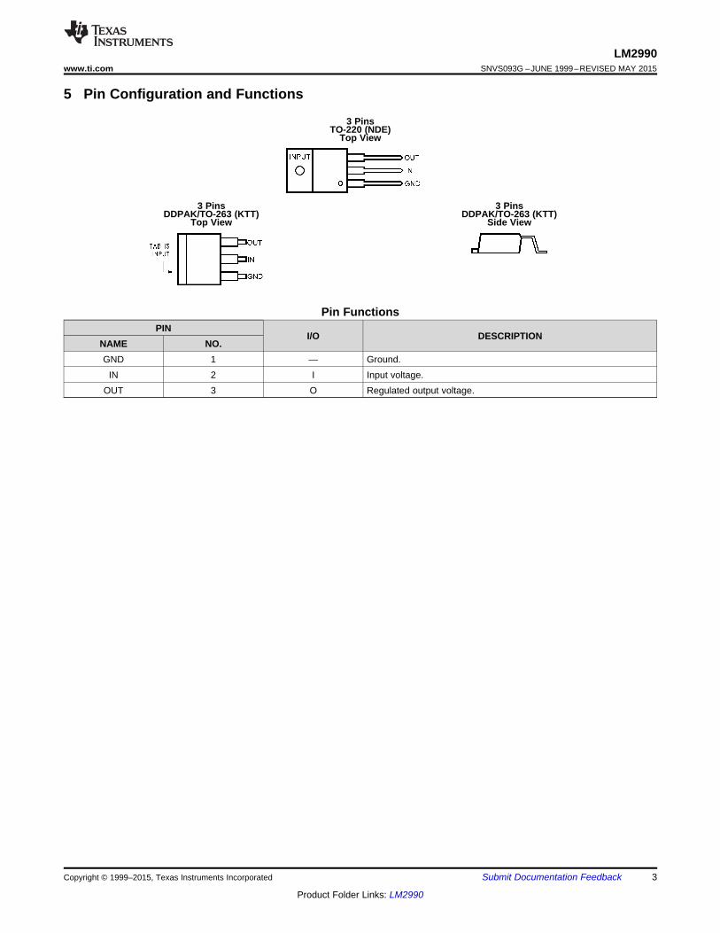
5 Pin Configuration and Functions
3 PinsTO-220 (NDE)
Top View
3 Pins 3 PinsDDPAK/TO-263 (KTT) DDPAK/TO-263 (KTT)
Top View Side View
Pin FunctionsPIN
I/O DESCRIPTIONNAME NO.GND 1 — Ground.
IN 2 I Input voltage.OUT 3 O Regulated output voltage.
Copyright © 1999–2015, Texas Instruments Incorporated Submit Documentation Feedback 3
Product Folder Links: LM2990

LM2990SNVS093G –JUNE 1999–REVISED MAY 2015 www.ti.com
6 Specifications
6.1 Absolute Maximum Ratingsover operating free-air temperature range (unless otherwise noted) (1) (2)
MIN MAX UNITInput voltage –26 0.3 VPower dissipation (3) Internally limitedJunction temperature (TJmax) 125 °CStorage temperature, Tstg –65 150 °C
(1) Stresses beyond those listed under Absolute Maximum Ratings may cause permanent damage to the device. These are stress ratingsonly, which do not imply functional operation of the device at these or any other conditions beyond those indicated under RecommendedOperating Conditions. Exposure to absolute-maximum-rated conditions for extended periods may affect device reliability.
(2) If Military/Aerospace specified devices are required, please contact the Texas Instruments Sales Office/Distributors for availability andspecifications.
(3) The maximum power dissipation is a function of TJmax, RθJA, and TA. The maximum allowable power dissipation at any ambienttemperature is PD = (TJmax − TA)/RθJA. If this dissipation is exceeded, the die temperature will rise above 125°C, and the LM2990 willeventually go into thermal shutdown at a TJ of approximately 160°C. Please refer to Thermal Information for more details.
6.2 ESD RatingsVALUE UNIT
V(ESD) Electrostatic discharge Human-body model (HBM), per ANSI/ESDA/JEDEC JS-001 (1) ±2000 V
(1) JEDEC document JEP155 states that 500-V HBM allows safe manufacturing with a standard ESD control process.
6.3 Recommended Operating Conditionsover operating free-air temperature range (unless otherwise noted) (1)
MIN NOM MAX UNITJunction temperature (TJ) –40 125 °CInput voltage (operational) –26 –6 V
(1) Stresses beyond those listed under Absolute Maximum Ratings may cause permanent damage to the device. These are stress ratingsonly, which do not imply functional operation of the device at these or any other conditions beyond those indicated under RecommendedOperating Conditions. Exposure to absolute-maximum-rated conditions for extended periods may affect device reliability.
6.4 Thermal InformationLM2990S LM2990T
THERMAL METRIC (1) TO-263 (KTT) TO-220 (NDE) UNIT3 PINS 3 PINS
RθJA Junction-to-ambient thermal resistance, High-K 41.3 22.8RθJC(top) Junction-to-case (top) thermal resistance 43 15.7RθJB Junction-to-board thermal resistance 23.2 4.2
°C/WψJT Junction-to-top characterization parameter 11.3 2.2ψJB Junction-to-board characterization parameter 20.4 4.2RθJC(bot) Junction-to-case (bottom) thermal resistance 0.5 0.7
(1) For more information about traditional and new thermal metrics, see the IC Package Thermal Metrics application report, SPRA953.
4 Submit Documentation Feedback Copyright © 1999–2015, Texas Instruments Incorporated
Product Folder Links: LM2990
LM2990www.ti.com SNVS093G –JUNE 1999–REVISED MAY 2015
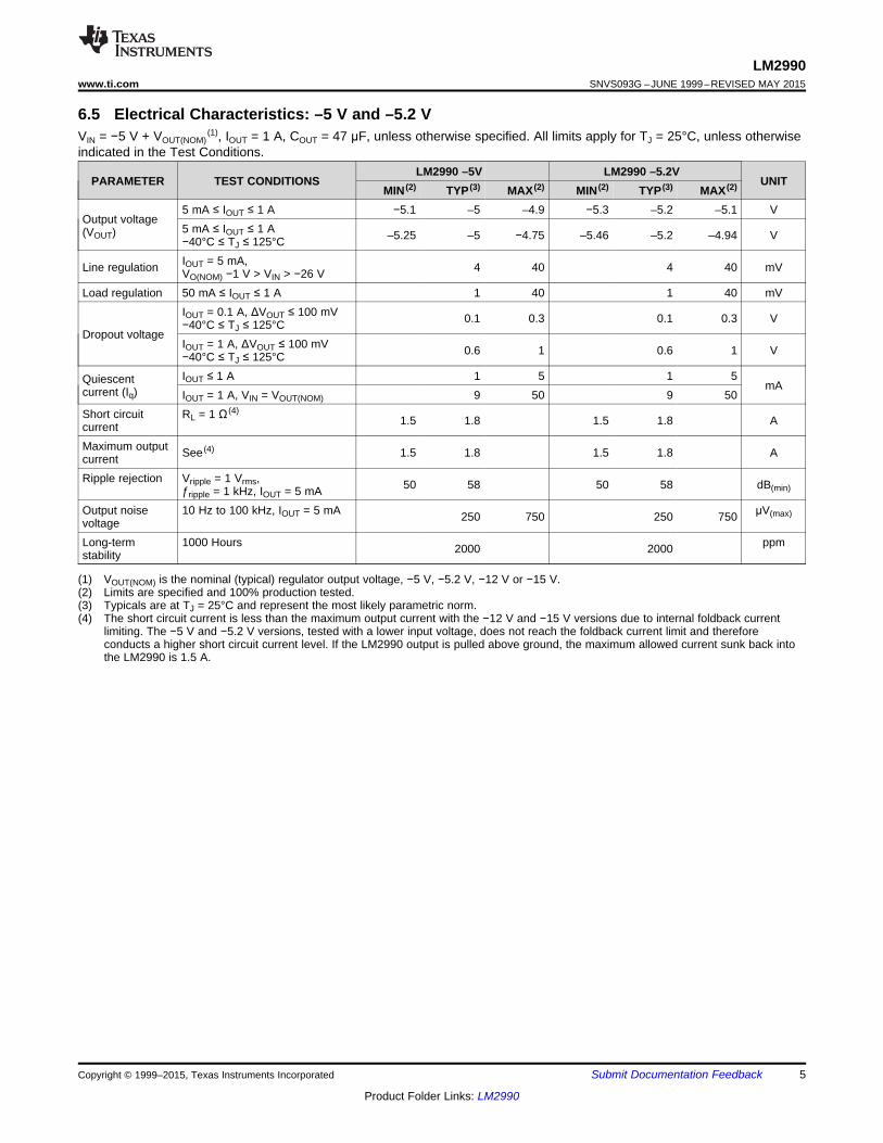
6.5 Electrical Characteristics: –5 V and –5.2 VVIN = −5 V + VOUT(NOM)
(1), IOUT = 1 A, COUT = 47 μF, unless otherwise specified. All limits apply for TJ = 25°C, unless otherwiseindicated in the Test Conditions.
LM2990 –5V LM2990 –5.2VPARAMETER TEST CONDITIONS UNIT
MIN (2) TYP (3) MAX (2) MIN (2) TYP (3) MAX (2)
5 mA ≤ IOUT ≤ 1 A −5.1 –5 –4.9 −5.3 –5.2 –5.1 VOutput voltage
5 mA ≤ IOUT ≤ 1 A(VOUT) –5.25 –5 −4.75 –5.46 –5.2 –4.94 V−40°C ≤ TJ ≤ 125°CIOUT = 5 mA,Line regulation 4 40 4 40 mVVO(NOM) −1 V > VIN > −26 V
Load regulation 50 mA ≤ IOUT ≤ 1 A 1 40 1 40 mVIOUT = 0.1 A, ΔVOUT ≤ 100 mV 0.1 0.3 0.1 0.3 V−40°C ≤ TJ ≤ 125°C
Dropout voltageIOUT = 1 A, ΔVOUT ≤ 100 mV 0.6 1 0.6 1 V−40°C ≤ TJ ≤ 125°CIOUT ≤ 1 A 1 5 1 5Quiescent mAcurrent (Iq) IOUT = 1 A, VIN = VOUT(NOM) 9 50 9 50
Short circuit RL = 1 Ω (4)1.5 1.8 1.5 1.8 Acurrent
Maximum output See (4) 1.5 1.8 1.5 1.8 AcurrentRipple rejection Vripple = 1 Vrms, 50 58 50 58 dB(min)ƒripple = 1 kHz, IOUT = 5 mAOutput noise 10 Hz to 100 kHz, IOUT = 5 mA μV(max)250 750 250 750voltageLong-term 1000 Hours ppm2000 2000stability
(1) VOUT(NOM) is the nominal (typical) regulator output voltage, −5 V, −5.2 V, −12 V or −15 V.(2) Limits are specified and 100% production tested.(3) Typicals are at TJ = 25°C and represent the most likely parametric norm.(4) The short circuit current is less than the maximum output current with the −12 V and −15 V versions due to internal foldback current
limiting. The −5 V and −5.2 V versions, tested with a lower input voltage, does not reach the foldback current limit and thereforeconducts a higher short circuit current level. If the LM2990 output is pulled above ground, the maximum allowed current sunk back intothe LM2990 is 1.5 A.
Copyright © 1999–2015, Texas Instruments Incorporated Submit Documentation Feedback 5
Product Folder Links: LM2990
LM2990SNVS093G –JUNE 1999–REVISED MAY 2015 www.ti.com
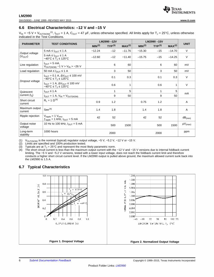
6.6 Electrical Characteristics: –12 V and –15 VVIN = −5 V + VOUT(NOM)
(1), IOUT = 1 A, COUT = 47 μF, unless otherwise specified. All limits apply for TJ = 25°C, unless otherwiseindicated in the Test Conditions.
LM2990 –12V LM2990 –15VPARAMETER TEST CONDITIONS UNIT
MIN (2) TYP (3) MAX (2) MIN (2) TYP (3) MAX (2)
5 mA ≤ IOUT ≤ 1 A −12.24 –12 –11.76 −15.30 –15 –14.70 VOutput voltage
5 mA ≤ IOUT ≤ 1 A(VOUT) –12.60 –12 −11.40 –15.75 –15 –14.25 V−40°C ≤ TJ ≤ 125°CIOUT = 5 mA,Line regulation 6 60 6 60 mVVOUT(NOM) −1 V > VIN > −26 V
Load regulation 50 mA ≤ IOUT ≤ 1 A 3 50 3 50 mVIOUT = 0.1 A, ΔVOUT ≤ 100 mV 0.1 0.3 0.1 0.3 V−40°C ≤ TJ ≤ 125°C
Dropout voltageIOUT = 1 A, ΔVOUT ≤ 100 mV 0.6 1 0.6 1 V−40°C ≤ TJ ≤ 125°CIOUT ≤ 1 A 1 5 1 5Quiescent mAcurrent (Iq) IOUT = 1 A, VIN = VOUT(NOM) 9 50 9 50
Short circuit RL = 1 Ω (4)0.9 1.2 0.75 1.2 Acurrent
Maximum output See (4) 1.4 1.8 1.4 1.8 AcurrentRipple rejection Vripple = 1 Vrms, 42 52 42 52 dB(min)ƒripple = 1 kHz, IOUT = 5 mAOutput noise 10 Hz to 100 kHz, IOUT = 5 mA μV(max)500 1500 500 1500voltageLong-term 1000 hours ppm2000 2000stability
(1) VOUT(NOM) is the nominal (typical) regulator output voltage, −5 V, −5.2 V, −12 V or −15 V.(2) Limits are specified and 100% production tested.(3) Typicals are at TJ = 25°C and represent the most likely parametric norm.(4) The short circuit current is less than the maximum output current with the −12 V and −15 V versions due to internal foldback current
limiting. The −5 V and −5.2 V versions, tested with a lower input voltage, does not reach the foldback current limit and thereforeconducts a higher short circuit current level. If the LM2990 output is pulled above ground, the maximum allowed current sunk back intothe LM2990 is 1.5 A.
6.7 Typical Characteristics
Figure 1. Dropout Voltage Figure 2. Normalized Output Voltage
6 Submit Documentation Feedback Copyright © 1999–2015, Texas Instruments Incorporated
Product Folder Links: LM2990

LM2990www.ti.com SNVS093G –JUNE 1999–REVISED MAY 2015
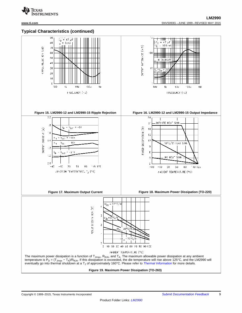
Typical Characteristics (continued)
Figure 3. LM2990-5.0 and LM2990-5.2 Quiescent Current Figure 4. LM2990-12 Quiescent Current
Figure 6. LM2990-5 and LM2990-5.2 Low Voltage BehaviorFigure 5. LM2990-15 Quiescent Current
Figure 8. LM2990-5 and LM2990-5.2 Load TransientFigure 7. LM2990-5 and LM2990-5.2 Line TransientResponseResponse
Copyright © 1999–2015, Texas Instruments Incorporated Submit Documentation Feedback 7
Product Folder Links: LM2990

LM2990SNVS093G –JUNE 1999–REVISED MAY 2015 www.ti.com
Typical Characteristics (continued)
Figure 10. LM2990-12 and LM2990-15 Line TransientFigure 9. LM2990-12 and LM2990-15 Low-Voltage BehaviorResponse
Figure 11. LM2990-12 and LM2990-15 Load TransientFigure 12. LM2990-5 and LM2990-5.2 Ripple RejectionResponse
Figure 13. LM2990-5 and LM2990-5.2 Output Impedance Figure 14. Maximum Output Current
8 Submit Documentation Feedback Copyright © 1999–2015, Texas Instruments Incorporated
Product Folder Links: LM2990
LM2990www.ti.com SNVS093G –JUNE 1999–REVISED MAY 2015
Typical Characteristics (continued)
Figure 15. LM2990-12 and LM2990-15 Ripple Rejection Figure 16. LM2990-12 and LM2990-15 Output Impedance
Figure 18. Maximum Power Dissipation (TO-220)Figure 17. Maximum Output Current
The maximum power dissipation is a function of TJmax, RθJA, and TA. The maximum allowable power dissipation at any ambienttemperature is PD = (TJmax − TA)/RθJA. If this dissipation is exceeded, the die temperature will rise above 125°C, and the LM2990 willeventually go into thermal shutdown at a TJ of approximately 160°C. Please refer to Thermal Information for more details.
Figure 19. Maximum Power Dissipation (TO-263)
Copyright © 1999–2015, Texas Instruments Incorporated Submit Documentation Feedback 9
Product Folder Links: LM2990
Reference
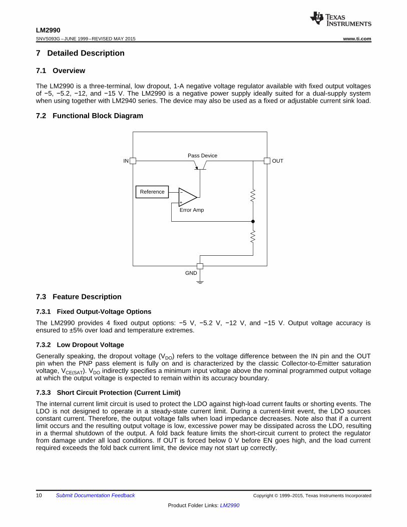
Pass Device
Error Amp
IN OUT
GND
LM2990SNVS093G –JUNE 1999–REVISED MAY 2015 www.ti.com
7 Detailed Description
7.1 Overview
The LM2990 is a three-terminal, low dropout, 1-A negative voltage regulator available with fixed output voltagesof −5, −5.2, −12, and −15 V. The LM2990 is a negative power supply ideally suited for a dual-supply systemwhen using together with LM2940 series. The device may also be used as a fixed or adjustable current sink load.
7.2 Functional Block Diagram
7.3 Feature Description
7.3.1 Fixed Output-Voltage OptionsThe LM2990 provides 4 fixed output options: −5 V, −5.2 V, −12 V, and −15 V. Output voltage accuracy isensured to ±5% over load and temperature extremes.
7.3.2 Low Dropout VoltageGenerally speaking, the dropout voltage (VDO) refers to the voltage difference between the IN pin and the OUTpin when the PNP pass element is fully on and is characterized by the classic Collector-to-Emitter saturationvoltage, VCE(SAT). VDO indirectly specifies a minimum input voltage above the nominal programmed output voltageat which the output voltage is expected to remain within its accuracy boundary.
7.3.3 Short Circuit Protection (Current Limit)The internal current limit circuit is used to protect the LDO against high-load current faults or shorting events. TheLDO is not designed to operate in a steady-state current limit. During a current-limit event, the LDO sourcesconstant current. Therefore, the output voltage falls when load impedance decreases. Note also that if a currentlimit occurs and the resulting output voltage is low, excessive power may be dissipated across the LDO, resultingin a thermal shutdown of the output. A fold back feature limits the short-circuit current to protect the regulatorfrom damage under all load conditions. If OUT is forced below 0 V before EN goes high, and the load currentrequired exceeds the fold back current limit, the device may not start up correctly.
10 Submit Documentation Feedback Copyright © 1999–2015, Texas Instruments Incorporated
Product Folder Links: LM2990

LM2990www.ti.com SNVS093G –JUNE 1999–REVISED MAY 2015
Feature Description (continued)7.3.4 Thermal ProtectionThe device contains a thermal shutdown protection circuit to turn off the output current when excessive heat isdissipated in the LDO. The thermal time-constant of the semiconductor die is fairly short, and thus the outputcycles on and off at a high rate when thermal shutdown is reached until the power dissipation is reduced. Theinternal protection circuitry of the device is designed to protect against thermal overload conditions. The circuitryis not intended to replace proper heat sinking. Continuously running the device into thermal shutdown degradesits reliability.
7.4 Device Functional Modes
7.4.1 Operation with VOUT(TARGET) –5 V ≥ VIN > –26 VThe device operates if the input voltage is within VOUT(TARGET) –5 V to –26 V range. At input voltages beyond theVIN requirement, the devices do not operate correctly, and output voltage may not reach target value.
Copyright © 1999–2015, Texas Instruments Incorporated Submit Documentation Feedback 11
Product Folder Links: LM2990

LM2990SNVS093G –JUNE 1999–REVISED MAY 2015 www.ti.com
8 Application and Implementation
NOTEInformation in the following applications sections is not part of the TI componentspecification, and TI does not warrant its accuracy or completeness. TI’s customers areresponsible for determining suitability of components for their purposes. Customers shouldvalidate and test their design implementation to confirm system functionality.
8.1 Application InformationThe LM2990 is a 1-A negative voltage regulator with an operating VIN range of –6 V to –26 V, and a regulatedVOUT having 5% accuracy with a maximum rated IOUT current of 1 A. Efficiency is defined by the ratio of outputvoltage to input voltage because the LM2990 is a linear voltage regulator. To achieve high efficiency, the dropoutvoltage (VIN – VOUT) must be as small as possible, thus requiring a very low dropout LDO.
Successfully implementing an LDO in an application depends on the application requirements. If therequirements are simply input voltage and output voltage, compliance specifications (such as internal powerdissipation or stability) must be verified to ensure a solid design. If timing, start-up, noise, PSRR, or any othertransient specification is required, the design becomes more challenging.
8.2 Typical Application
8.2.1 –5 V Post Regulator for an Isolated Switching Power Supply
Figure 20. Post Regulator for an Isolated Switching Power Supply
8.2.1.1 Design RequirementsFor this design example, use the parameters listed in Table 1 as the input parameters.
Table 1. Design ParametersDESIGN PARAMETER DESIGN REQUIREMENT
Input voltage –10 V, provided by the DC-DC converter switching at 1 MHzOutput voltage -5 V, ±10%Output current 5 mA to 400 mA
RMS noise, 10 Hz to 100 kHz < 1 mVRMS, IOUT = 5 mAPSRR at 1KHz > 45 dB, IOUT = 5 mA
8.2.1.2 Detailed Design ProcedureAt 400-mA loading, the dropout of the LM2990 has 1-V maximum dropout over temperature, thus an –5 Vheadroom is sufficient for operation over both input and output voltage accuracy. The efficiency of the LM2990 inthis configuration is VOUT / VIN = 50%.
To achieve the smallest form factor, the TO-263(KTT) package is selected. Input and output capacitors should beselected in accordance with the External Capacitors section. Aluminum capacitances of 470 μF for the input and50-μF capacitors for the output are selected. With an efficiency of 50% and a 400-mA maximum load, the internalpower dissipation is 2000 mW, which corresponds to 82.5°C junction temperature rise for the TO-263 package.With an 25°C ambient temperature, the junction temperature is at 107.5°C.
12 Submit Documentation Feedback Copyright © 1999–2015, Texas Instruments Incorporated
Product Folder Links: LM2990
LM2990www.ti.com SNVS093G –JUNE 1999–REVISED MAY 2015
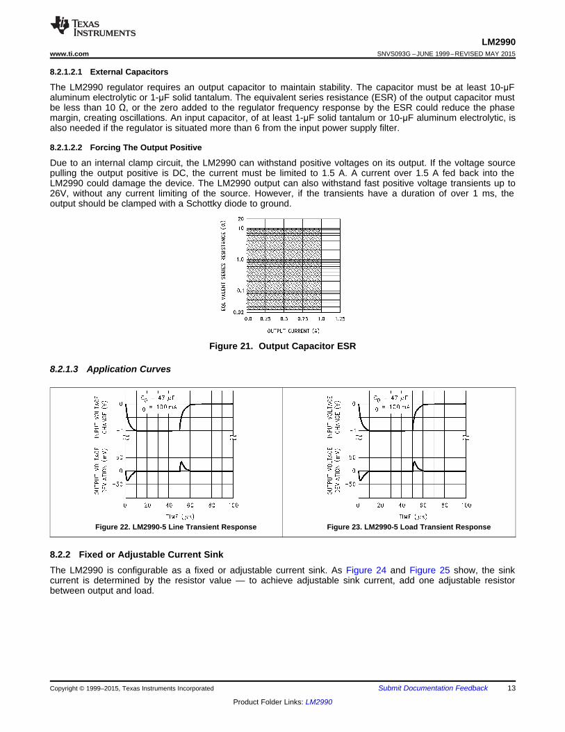
8.2.1.2.1 External Capacitors
The LM2990 regulator requires an output capacitor to maintain stability. The capacitor must be at least 10-μFaluminum electrolytic or 1-μF solid tantalum. The equivalent series resistance (ESR) of the output capacitor mustbe less than 10 Ω, or the zero added to the regulator frequency response by the ESR could reduce the phasemargin, creating oscillations. An input capacitor, of at least 1-μF solid tantalum or 10-μF aluminum electrolytic, isalso needed if the regulator is situated more than 6 from the input power supply filter.
8.2.1.2.2 Forcing The Output Positive
Due to an internal clamp circuit, the LM2990 can withstand positive voltages on its output. If the voltage sourcepulling the output positive is DC, the current must be limited to 1.5 A. A current over 1.5 A fed back into theLM2990 could damage the device. The LM2990 output can also withstand fast positive voltage transients up to26V, without any current limiting of the source. However, if the transients have a duration of over 1 ms, theoutput should be clamped with a Schottky diode to ground.
Figure 21. Output Capacitor ESR
8.2.1.3 Application Curves
Figure 22. LM2990-5 Line Transient Response Figure 23. LM2990-5 Load Transient Response
8.2.2 Fixed or Adjustable Current SinkThe LM2990 is configurable as a fixed or adjustable current sink. As Figure 24 and Figure 25 show, the sinkcurrent is determined by the resistor value — to achieve adjustable sink current, add one adjustable resistorbetween output and load.
Copyright © 1999–2015, Texas Instruments Incorporated Submit Documentation Feedback 13
Product Folder Links: LM2990

LM2990SNVS093G –JUNE 1999–REVISED MAY 2015 www.ti.com
Figure 24. Fixed Current Sink Figure 25. Adjustable Current Sink
8.2.2.1 Design RequirementsSee Design Requirements.
8.2.2.2 Detailed Design ProcedureSee Detailed Design Procedure.
8.2.2.3 Application CurvesSee Application Curves.
9 Power Supply RecommendationsThe LM2990 is designed to operate from an input voltage supply range between –6 V and –26 V. The inputvoltage range should provides adequate headroom in order for the device to have a regulated output. This inputsupply must be well regulated.
14 Submit Documentation Feedback Copyright © 1999–2015, Texas Instruments Incorporated
Product Folder Links: LM2990
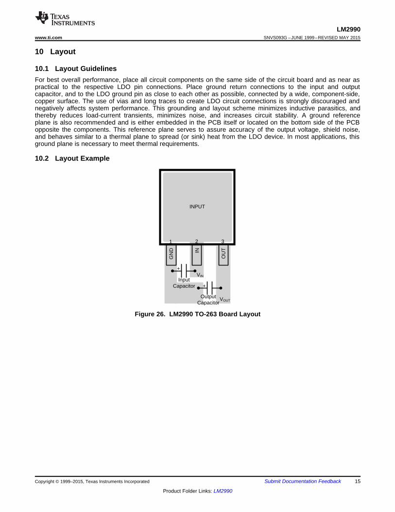
1 2 3
IN
GN
D
OU
T
VINInput
Capacitor
VOUTOutput
Capacitor
INPUT
+
+
LM2990www.ti.com SNVS093G –JUNE 1999–REVISED MAY 2015
10 Layout
10.1 Layout GuidelinesFor best overall performance, place all circuit components on the same side of the circuit board and as near aspractical to the respective LDO pin connections. Place ground return connections to the input and outputcapacitor, and to the LDO ground pin as close to each other as possible, connected by a wide, component-side,copper surface. The use of vias and long traces to create LDO circuit connections is strongly discouraged andnegatively affects system performance. This grounding and layout scheme minimizes inductive parasitics, andthereby reduces load-current transients, minimizes noise, and increases circuit stability. A ground referenceplane is also recommended and is either embedded in the PCB itself or located on the bottom side of the PCBopposite the components. This reference plane serves to assure accuracy of the output voltage, shield noise,and behaves similar to a thermal plane to spread (or sink) heat from the LDO device. In most applications, thisground plane is necessary to meet thermal requirements.
10.2 Layout Example
Figure 26. LM2990 TO-263 Board Layout
Copyright © 1999–2015, Texas Instruments Incorporated Submit Documentation Feedback 15
Product Folder Links: LM2990
LM2990SNVS093G –JUNE 1999–REVISED MAY 2015 www.ti.com
11 Device and Documentation Support
11.1 Device Support
11.1.1 Device Nomenclature
Dropout Voltage: The input-output voltage differential at which the circuit ceases to regulate against furtherreduction in input voltage. Measured when the output voltage has dropped 100 mV from thenominal value obtained at (VOUT + 5 V) input, dropout voltage is dependent upon load current andjunction temperature.
Input Voltage: The DC voltage applied to the input terminals with respect to ground.
Input-Output Differential: The voltage difference between the unregulated input voltage and the regulatedoutput voltage for which the regulator will operate.
Line Regulation: The change in output voltage for a change in the input voltage. The measurement is madeunder conditions of low dissipation or by using pulse techniques such that the average chiptemperature is not significantly affected.
Load Regulation: The change in output voltage for a change in load current at constant chip temperature.
Long Term Stability: Output voltage stability under accelerated life-test conditions after 1000 hours withmaximum rated voltage and junction temperature.
Output Noise Voltage: The rms AC voltage at the output, with constant load and no input ripple, measured overa specified frequency range.
Quiescent Current: That part of the positive input current that does not contribute to the positive load current.The regulator ground lead current.
Ripple Rejection: The ratio of the peak-to-peak input ripple voltage to the peak-to-peak output ripple voltage.
Temperature Stability of VOUT: The percentage change in output voltage for a thermal variation from roomtemperature to either temperature extreme.
11.2 TrademarksAll trademarks are the property of their respective owners.
11.3 Electrostatic Discharge CautionThese devices have limited built-in ESD protection. The leads should be shorted together or the device placed in conductive foamduring storage or handling to prevent electrostatic damage to the MOS gates.
11.4 GlossarySLYZ022 — TI Glossary.
This glossary lists and explains terms, acronyms, and definitions.
12 Mechanical, Packaging, and Orderable InformationThe following pages include mechanical, packaging, and orderable information. This information is the mostcurrent data available for the designated devices. This data is subject to change without notice and revision ofthis document. For browser-based versions of this data sheet, refer to the left-hand navigation.
16 Submit Documentation Feedback Copyright © 1999–2015, Texas Instruments Incorporated
Product Folder Links: LM2990
PACKAGE OPTION ADDENDUM
www.ti.com 27-Oct-2016
Addendum-Page 1
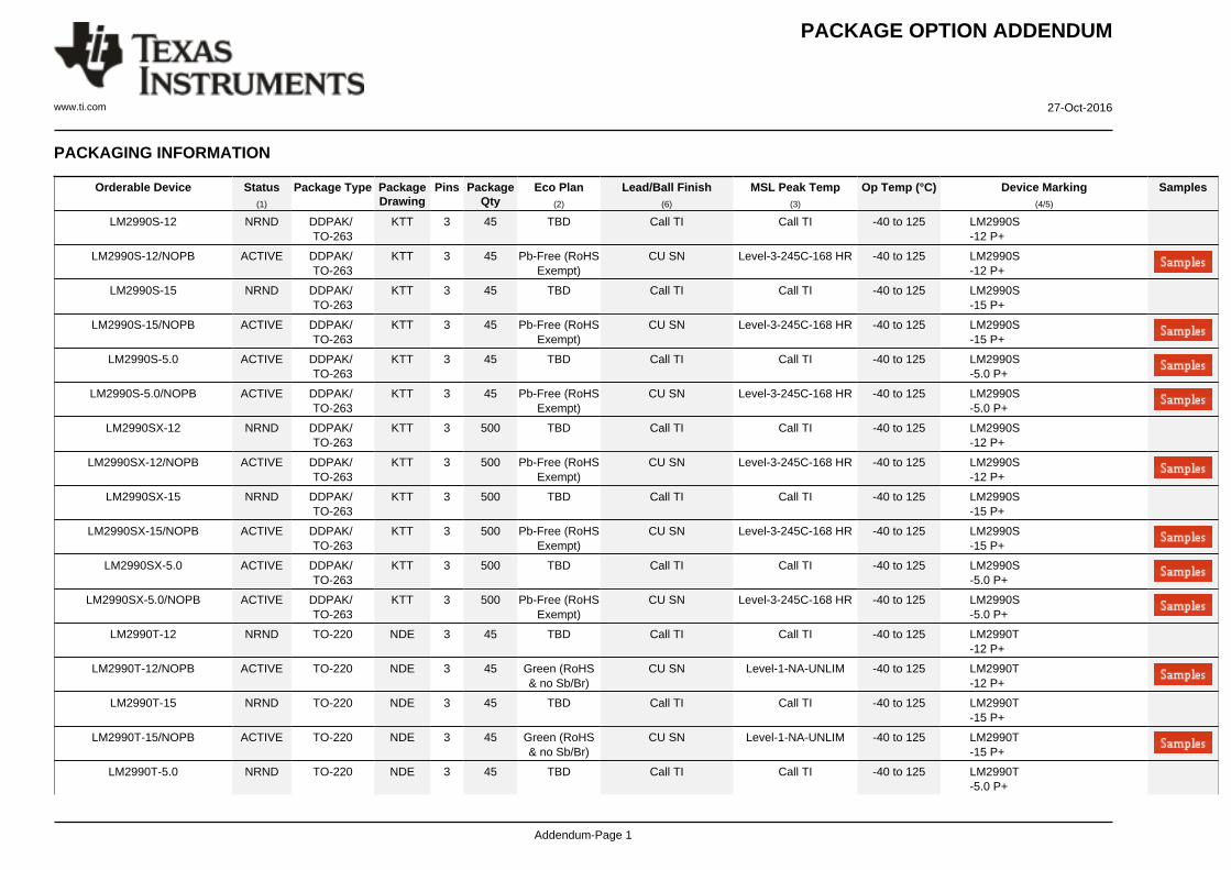
PACKAGING INFORMATION
Orderable Device Status(1)
Package Type PackageDrawing
Pins PackageQty
Eco Plan(2)
Lead/Ball Finish(6)
MSL Peak Temp(3)
Op Temp (°C) Device Marking(4/5)
Samples
LM2990S-12 NRND DDPAK/TO-263
KTT 3 45 TBD Call TI Call TI -40 to 125 LM2990S-12 P+
LM2990S-12/NOPB ACTIVE DDPAK/TO-263
KTT 3 45 Pb-Free (RoHSExempt)
CU SN Level-3-245C-168 HR -40 to 125 LM2990S-12 P+
LM2990S-15 NRND DDPAK/TO-263
KTT 3 45 TBD Call TI Call TI -40 to 125 LM2990S-15 P+
LM2990S-15/NOPB ACTIVE DDPAK/TO-263
KTT 3 45 Pb-Free (RoHSExempt)
CU SN Level-3-245C-168 HR -40 to 125 LM2990S-15 P+
LM2990S-5.0 ACTIVE DDPAK/TO-263
KTT 3 45 TBD Call TI Call TI -40 to 125 LM2990S-5.0 P+
LM2990S-5.0/NOPB ACTIVE DDPAK/TO-263
KTT 3 45 Pb-Free (RoHSExempt)
CU SN Level-3-245C-168 HR -40 to 125 LM2990S-5.0 P+
LM2990SX-12 NRND DDPAK/TO-263
KTT 3 500 TBD Call TI Call TI -40 to 125 LM2990S-12 P+
LM2990SX-12/NOPB ACTIVE DDPAK/TO-263
KTT 3 500 Pb-Free (RoHSExempt)
CU SN Level-3-245C-168 HR -40 to 125 LM2990S-12 P+
LM2990SX-15 NRND DDPAK/TO-263
KTT 3 500 TBD Call TI Call TI -40 to 125 LM2990S-15 P+
LM2990SX-15/NOPB ACTIVE DDPAK/TO-263
KTT 3 500 Pb-Free (RoHSExempt)
CU SN Level-3-245C-168 HR -40 to 125 LM2990S-15 P+
LM2990SX-5.0 ACTIVE DDPAK/TO-263
KTT 3 500 TBD Call TI Call TI -40 to 125 LM2990S-5.0 P+
LM2990SX-5.0/NOPB ACTIVE DDPAK/TO-263
KTT 3 500 Pb-Free (RoHSExempt)
CU SN Level-3-245C-168 HR -40 to 125 LM2990S-5.0 P+
LM2990T-12 NRND TO-220 NDE 3 45 TBD Call TI Call TI -40 to 125 LM2990T-12 P+
LM2990T-12/NOPB ACTIVE TO-220 NDE 3 45 Green (RoHS& no Sb/Br)
CU SN Level-1-NA-UNLIM -40 to 125 LM2990T-12 P+
LM2990T-15 NRND TO-220 NDE 3 45 TBD Call TI Call TI -40 to 125 LM2990T-15 P+
LM2990T-15/NOPB ACTIVE TO-220 NDE 3 45 Green (RoHS& no Sb/Br)
CU SN Level-1-NA-UNLIM -40 to 125 LM2990T-15 P+
LM2990T-5.0 NRND TO-220 NDE 3 45 TBD Call TI Call TI -40 to 125 LM2990T-5.0 P+

PACKAGE OPTION ADDENDUM
www.ti.com 27-Oct-2016
Addendum-Page 2
Orderable Device Status(1)
Package Type PackageDrawing
Pins PackageQty
Eco Plan(2)
Lead/Ball Finish(6)
MSL Peak Temp(3)
Op Temp (°C) Device Marking(4/5)
Samples
LM2990T-5.0/NOPB ACTIVE TO-220 NDE 3 45 Pb-Free (RoHSExempt)
CU SN Level-1-NA-UNLIM -40 to 125 LM2990T-5.0 P+
LM2990T-5.2/NOPB ACTIVE TO-220 NDE 3 45 Green (RoHS& no Sb/Br)
CU SN Level-1-NA-UNLIM -40 to 125 LM2990T-5.2 P+
(1) The marketing status values are defined as follows:ACTIVE: Product device recommended for new designs.LIFEBUY: TI has announced that the device will be discontinued, and a lifetime-buy period is in effect.NRND: Not recommended for new designs. Device is in production to support existing customers, but TI does not recommend using this part in a new design.PREVIEW: Device has been announced but is not in production. Samples may or may not be available.OBSOLETE: TI has discontinued the production of the device.
(2) Eco Plan - The planned eco-friendly classification: Pb-Free (RoHS), Pb-Free (RoHS Exempt), or Green (RoHS & no Sb/Br) - please check http://www.ti.com/productcontent for the latest availabilityinformation and additional product content details.TBD: The Pb-Free/Green conversion plan has not been defined.Pb-Free (RoHS): TI's terms "Lead-Free" or "Pb-Free" mean semiconductor products that are compatible with the current RoHS requirements for all 6 substances, including the requirement thatlead not exceed 0.1% by weight in homogeneous materials. Where designed to be soldered at high temperatures, TI Pb-Free products are suitable for use in specified lead-free processes.Pb-Free (RoHS Exempt): This component has a RoHS exemption for either 1) lead-based flip-chip solder bumps used between the die and package, or 2) lead-based die adhesive used betweenthe die and leadframe. The component is otherwise considered Pb-Free (RoHS compatible) as defined above.Green (RoHS & no Sb/Br): TI defines "Green" to mean Pb-Free (RoHS compatible), and free of Bromine (Br) and Antimony (Sb) based flame retardants (Br or Sb do not exceed 0.1% by weightin homogeneous material)
(3) MSL, Peak Temp. - The Moisture Sensitivity Level rating according to the JEDEC industry standard classifications, and peak solder temperature.
(4) There may be additional marking, which relates to the logo, the lot trace code information, or the environmental category on the device.
(5) Multiple Device Markings will be inside parentheses. Only one Device Marking contained in parentheses and separated by a "~" will appear on a device. If a line is indented then it is a continuationof the previous line and the two combined represent the entire Device Marking for that device.
(6) Lead/Ball Finish - Orderable Devices may have multiple material finish options. Finish options are separated by a vertical ruled line. Lead/Ball Finish values may wrap to two lines if the finishvalue exceeds the maximum column width.
Important Information and Disclaimer:The information provided on this page represents TI's knowledge and belief as of the date that it is provided. TI bases its knowledge and belief on informationprovided by third parties, and makes no representation or warranty as to the accuracy of such information. Efforts are underway to better integrate information from third parties. TI has taken andcontinues to take reasonable steps to provide representative and accurate information but may not have conducted destructive testing or chemical analysis on incoming materials and chemicals.TI and TI suppliers consider certain information to be proprietary, and thus CAS numbers and other limited information may not be available for release.
In no event shall TI's liability arising out of such information exceed the total purchase price of the TI part(s) at issue in this document sold by TI to Customer on an annual basis.
PACKAGE OPTION ADDENDUM
www.ti.com 27-Oct-2016
Addendum-Page 3

TAPE AND REEL INFORMATION
*All dimensions are nominal
Device PackageType
PackageDrawing
Pins SPQ ReelDiameter
(mm)
ReelWidth
W1 (mm)
A0(mm)
B0(mm)
K0(mm)
P1(mm)
W(mm)
Pin1Quadrant
LM2990SX-12 DDPAK/TO-263
KTT 3 500 330.0 24.4 10.75 14.85 5.0 16.0 24.0 Q2
LM2990SX-12/NOPB DDPAK/TO-263
KTT 3 500 330.0 24.4 10.75 14.85 5.0 16.0 24.0 Q2
LM2990SX-15 DDPAK/TO-263
KTT 3 500 330.0 24.4 10.75 14.85 5.0 16.0 24.0 Q2
LM2990SX-15/NOPB DDPAK/TO-263
KTT 3 500 330.0 24.4 10.75 14.85 5.0 16.0 24.0 Q2
LM2990SX-5.0 DDPAK/TO-263
KTT 3 500 330.0 24.4 10.75 14.85 5.0 16.0 24.0 Q2
LM2990SX-5.0/NOPB DDPAK/TO-263
KTT 3 500 330.0 24.4 10.75 14.85 5.0 16.0 24.0 Q2
PACKAGE MATERIALS INFORMATION
www.ti.com 14-Feb-2015
Pack Materials-Page 1
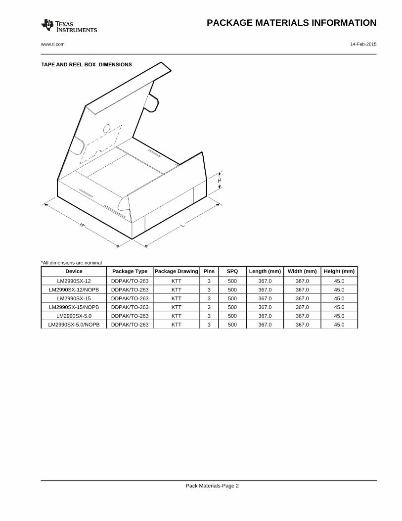
*All dimensions are nominal
Device Package Type Package Drawing Pins SPQ Length (mm) Width (mm) Height (mm)
LM2990SX-12 DDPAK/TO-263 KTT 3 500 367.0 367.0 45.0
LM2990SX-12/NOPB DDPAK/TO-263 KTT 3 500 367.0 367.0 45.0
LM2990SX-15 DDPAK/TO-263 KTT 3 500 367.0 367.0 45.0
LM2990SX-15/NOPB DDPAK/TO-263 KTT 3 500 367.0 367.0 45.0
LM2990SX-5.0 DDPAK/TO-263 KTT 3 500 367.0 367.0 45.0
LM2990SX-5.0/NOPB DDPAK/TO-263 KTT 3 500 367.0 367.0 45.0
PACKAGE MATERIALS INFORMATION
www.ti.com 14-Feb-2015
Pack Materials-Page 2
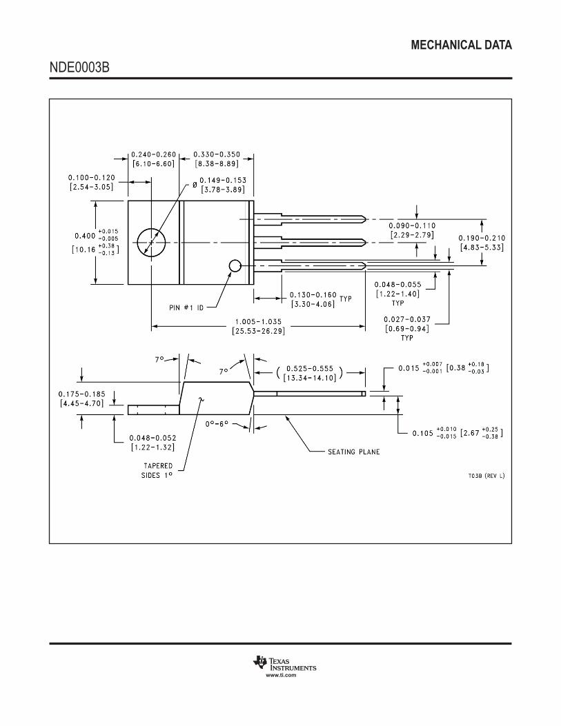
MECHANICAL DATA
NDE0003B
www.ti.com
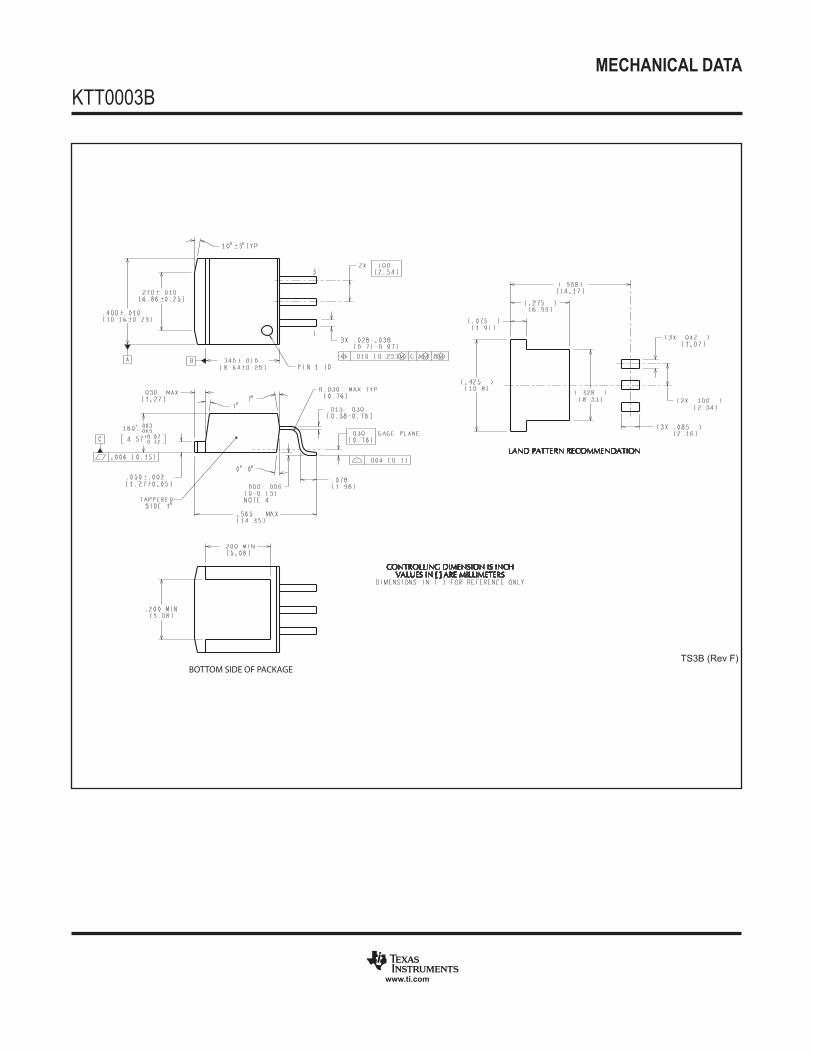
MECHANICAL DATA
KTT0003B
www.ti.com
BOTTOM SIDE OF PACKAGETS3B (Rev F)

IMPORTANT NOTICE
Texas Instruments Incorporated and its subsidiaries (TI) reserve the right to make corrections, enhancements, improvements and otherchanges to its semiconductor products and services per JESD46, latest issue, and to discontinue any product or service per JESD48, latestissue. Buyers should obtain the latest relevant information before placing orders and should verify that such information is current andcomplete. All semiconductor products (also referred to herein as “components”) are sold subject to TI’s terms and conditions of salesupplied at the time of order acknowledgment.TI warrants performance of its components to the specifications applicable at the time of sale, in accordance with the warranty in TI’s termsand conditions of sale of semiconductor products. Testing and other quality control techniques are used to the extent TI deems necessaryto support this warranty. Except where mandated by applicable law, testing of all parameters of each component is not necessarilyperformed.TI assumes no liability for applications assistance or the design of Buyers’ products. Buyers are responsible for their products andapplications using TI components. To minimize the risks associated with Buyers’ products and applications, Buyers should provideadequate design and operating safeguards.TI does not warrant or represent that any license, either express or implied, is granted under any patent right, copyright, mask work right, orother intellectual property right relating to any combination, machine, or process in which TI components or services are used. Informationpublished by TI regarding third-party products or services does not constitute a license to use such products or services or a warranty orendorsement thereof. Use of such information may require a license from a third party under the patents or other intellectual property of thethird party, or a license from TI under the patents or other intellectual property of TI.Reproduction of significant portions of TI information in TI data books or data sheets is permissible only if reproduction is without alterationand is accompanied by all associated warranties, conditions, limitations, and notices. TI is not responsible or liable for such altereddocumentation. Information of third parties may be subject to additional restrictions.Resale of TI components or services with statements different from or beyond the parameters stated by TI for that component or servicevoids all express and any implied warranties for the associated TI component or service and is an unfair and deceptive business practice.TI is not responsible or liable for any such statements.Buyer acknowledges and agrees that it is solely responsible for compliance with all legal, regulatory and safety-related requirementsconcerning its products, and any use of TI components in its applications, notwithstanding any applications-related information or supportthat may be provided by TI. Buyer represents and agrees that it has all the necessary expertise to create and implement safeguards whichanticipate dangerous consequences of failures, monitor failures and their consequences, lessen the likelihood of failures that might causeharm and take appropriate remedial actions. Buyer will fully indemnify TI and its representatives against any damages arising out of the useof any TI components in safety-critical applications.In some cases, TI components may be promoted specifically to facilitate safety-related applications. With such components, TI’s goal is tohelp enable customers to design and create their own end-product solutions that meet applicable functional safety standards andrequirements. Nonetheless, such components are subject to these terms.No TI components are authorized for use in FDA Class III (or similar life-critical medical equipment) unless authorized officers of the partieshave executed a special agreement specifically governing such use.Only those TI components which TI has specifically designated as military grade or “enhanced plastic” are designed and intended for use inmilitary/aerospace applications or environments. Buyer acknowledges and agrees that any military or aerospace use of TI componentswhich have not been so designated is solely at the Buyer's risk, and that Buyer is solely responsible for compliance with all legal andregulatory requirements in connection with such use.TI has specifically designated certain components as meeting ISO/TS16949 requirements, mainly for automotive use. In any case of use ofnon-designated products, TI will not be responsible for any failure to meet ISO/TS16949.
Products ApplicationsAudio www.ti.com/audio Automotive and Transportation www.ti.com/automotiveAmplifiers amplifier.ti.com Communications and Telecom www.ti.com/communicationsData Converters dataconverter.ti.com Computers and Peripherals www.ti.com/computersDLP® Products www.dlp.com Consumer Electronics www.ti.com/consumer-appsDSP dsp.ti.com Energy and Lighting www.ti.com/energyClocks and Timers www.ti.com/clocks Industrial www.ti.com/industrialInterface interface.ti.com Medical www.ti.com/medicalLogic logic.ti.com Security www.ti.com/securityPower Mgmt power.ti.com Space, Avionics and Defense www.ti.com/space-avionics-defenseMicrocontrollers microcontroller.ti.com Video and Imaging www.ti.com/videoRFID www.ti-rfid.comOMAP Applications Processors www.ti.com/omap TI E2E Community e2e.ti.comWireless Connectivity www.ti.com/wirelessconnectivity
Mailing Address: Texas Instruments, Post Office Box 655303, Dallas, Texas 75265Copyright © 2016, Texas Instruments Incorporated