lm3648 synchronous boost led flash drvr w/ 1.5-a hi-side ... · pdf filein hwen lm3648 sda scl...
TRANSCRIPT
IN
HWEN
LM3648
SDA
SCL
SW
OUT
LEDSTROBE
TORCH/TEMP
GNDTX
10 PF
10 PF
C2
L1
C1
D1
PP/PC
VIN
2.5V t 5.5V
1 PH
Product
Folder
Sample &Buy
Technical
Documents
Tools &
Software
Support &Community
An IMPORTANT NOTICE at the end of this data sheet addresses availability, warranty, changes, use in safety-critical applications,intellectual property matters and other important disclaimers. PRODUCTION DATA.
LM3648, LM3648TTSNVSA68D –OCTOBER 2014–REVISED NOVEMBER 2016
LM3648 Synchronous Boost LED Flash Driver with 1.5-A High-Side Current Source
1
1 Features1• 1.5-A LED Current Source Programmability• Accurate and Programmable LED Current Range
from 1.954 mA to 1.5 A• Torch Currents up to 500 mA (LM3648TT)• Flash Timeout Values up to 1.6 Seconds
(LM3648TT)• Optimized Flash LED Current During Low Battery
Conditions (IVFM)• > 85% Efficiency in Torch Mode (at 100 mA) and
Flash Mode (at 1 A to 1.5 A)• Grounded Cathode LED Operation for Improved
Thermal Management• Small Solution Size: < 16 mm2
• Hardware Strobe Enable (STROBE)• Synchronization Input for RF Power Amplifier
Pulse Events (TX)• Hardware Torch Enable (TORCH/TEMP)• Remote NTC Monitoring (TORCH/TEMP)• 400-kHz I2C-Compatible Interface
– LM3648 (I2C Address = 0x63)
2 Applications• Camera Phone White-LED Flash• Digital Still Cameras• Fire-Alarm Notification• Emergency Strobe Lighting• Intruder Alert Notification• Barcode Scanners• Handheld Data Terminals
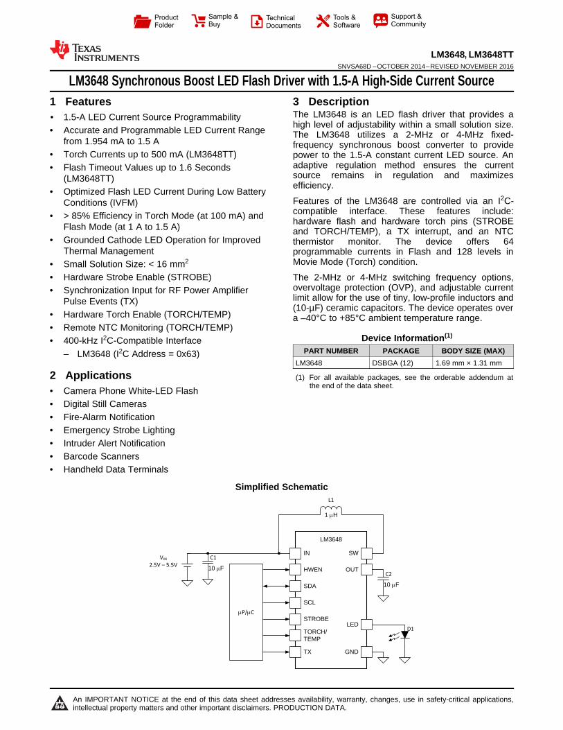
3 DescriptionThe LM3648 is an LED flash driver that provides ahigh level of adjustability within a small solution size.The LM3648 utilizes a 2-MHz or 4-MHz fixed-frequency synchronous boost converter to providepower to the 1.5-A constant current LED source. Anadaptive regulation method ensures the currentsource remains in regulation and maximizesefficiency.
Features of the LM3648 are controlled via an I2C-compatible interface. These features include:hardware flash and hardware torch pins (STROBEand TORCH/TEMP), a TX interrupt, and an NTCthermistor monitor. The device offers 64programmable currents in Flash and 128 levels inMovie Mode (Torch) condition.
The 2-MHz or 4-MHz switching frequency options,overvoltage protection (OVP), and adjustable currentlimit allow for the use of tiny, low-profile inductors and(10-µF) ceramic capacitors. The device operates overa –40°C to +85°C ambient temperature range.
Device Information(1)
PART NUMBER PACKAGE BODY SIZE (MAX)LM3648 DSBGA (12) 1.69 mm × 1.31 mm
(1) For all available packages, see the orderable addendum atthe end of the data sheet.
Simplified Schematic

2
LM3648, LM3648TTSNVSA68D –OCTOBER 2014–REVISED NOVEMBER 2016 www.ti.com
Product Folder Links: LM3648 LM3648TT
Submit Documentation Feedback Copyright © 2014–2016, Texas Instruments Incorporated
Table of Contents1 Features .................................................................. 12 Applications ........................................................... 13 Description ............................................................. 14 Revision History..................................................... 25 Pin Configuration and Functions ......................... 36 Specifications......................................................... 4
6.1 Absolute Maximum Ratings ...................................... 46.2 ESD Ratings.............................................................. 46.3 Recommended Operating Conditions....................... 46.4 Thermal Information .................................................. 46.5 Electrical Characteristics........................................... 56.6 Timing Requirements ............................................... 56.7 Switching Characteristics .......................................... 66.8 Typical Characteristics .............................................. 6
7 Detailed Description ............................................ 107.1 Overview ................................................................. 107.2 Functional Block Diagram ...................................... 117.3 Feature Description ................................................ 117.4 Device Functioning Modes...................................... 13
7.5 Programming........................................................... 167.6 Register Descriptions .............................................. 18
8 Applications and Implementation ...................... 228.1 Application Information............................................ 228.2 Typical Application ................................................. 22
9 Power Supply Recommendations ...................... 2710 Layout................................................................... 27
10.1 Layout Guidelines ................................................. 2710.2 Layout Example ................................................... 28
11 Device and Documentation Support ................. 2911.1 Device Support...................................................... 2911.2 Documentation Support ........................................ 2911.3 Receiving Notification of Documentation Updates 2911.4 Community Resources.......................................... 2911.5 Trademarks ........................................................... 2911.6 Electrostatic Discharge Caution............................ 2911.7 Glossary ................................................................ 30
12 Mechanical, Packaging, and OrderableInformation ........................................................... 30
4 Revision HistoryNOTE: Page numbers for previous revisions may differ from page numbers in the current version.
Changes from Revision C (September 2016) to Revision D Page
• Changed "(Default)" from "011111 = 748.75 mA" to "111111 = 1.5 A" in LED Flash Brightness Register ......................... 19
Changes from Revision B (September 2015) to Revision C Page
• Added several additional Applications ................................................................................................................................... 1
Changes from Revision A (August 2015) to Revision B Page
• Added "or 0x04 for LM3648TT" to Device ID Register row, Register Descriptions table..................................................... 18• Changed "'011'" to "'000'" in Device Register Bits 5-3 description....................................................................................... 21
Changes from Original (October 2014) to Revision A Page
• Added Torch Currents up to 500 mA (LM3648TT)................................................................................................................. 1• Added Flash Timeout Values up to 1.6 seconds (LM3648TT) .............................................................................................. 1• Changed Handling Ratings to ESD Ratings; moved storage temperature to Abs Max ......................................................... 4• Added ILED row for LM3648TT option .................................................................................................................................... 5• Added VHR row for LM3648TT option .................................................................................................................................... 5• Added several new graphs related to LM3648TT option performance ................................................................................. 5• Added to 1.6 s on LM3648TT in Flash Time-Out ................................................................................................................. 15• Added new eq. and LM3648TT values in LED Torch Brightness Reg.; added NOTE below LED Torch Brightness
Reg. description ................................................................................................................................................................... 19• Added LM3648TT values for Timing Config. Reg.; added NOTE below Timing Config. Reg. description ......................... 20• Added "or '100'" for LM3648TT in Device ID Register Bits 2-0 description ......................................................................... 21• Added Application curves for LM3648TT performance ....................................................................................................... 24

Top View
A1 A2
B1 B2 B3
Top View
A3
C2C1 C3
D2 D3D1
Pin A1
3
LM3648, LM3648TTwww.ti.com SNVSA68D –OCTOBER 2014–REVISED NOVEMBER 2016
Product Folder Links: LM3648 LM3648TT
Submit Documentation FeedbackCopyright © 2014–2016, Texas Instruments Incorporated
(1) A: Analog Pin, G: Ground Pin, P: Power Pin, I: Digital Input Pin
5 Pin Configuration and Functions
YFF Package12-Pin DSBGA
Pin FunctionsPIN
TYPE (1) DESCRIPTIONNUMBER NAMEA1 GND G Ground
A2 IN P Input voltage connection. Connect IN to the input supply and bypass to GND with a 10-µF or larger ceramic capacitor.
A3 SDA I/O Serial data input/output in the I2C Mode on LM3648.B1 SW P Drain connection for Internal NMOS and synchronous PMOS Switches.
B2 STROBE I Active high hardware flash enable. Drive STROBE high to turn on Flash pulse. Internalpulldown resistor of 300 kΩ between STROBE and GND.
B3 SCL I Serial clock input for LM3648.
C1 OUT P Step-up DC-DC converter output. Connect a 10-µF ceramic capacitor between thisterminal and GND.
C2 HWEN I Active high enable pin. High = Standby, Low = Shutdown/Reset. Internal pulldownresistor of 300 kΩ between HWEN and GND.
C3 TORCH/TEMP I/P Torch terminal input or threshold detector for NTC temperature sensing and currentscale back.
D1 LED P High-side current source output for flash LED. Connect pin D1 to D3 externally.
D2 TX I Configurable dual polarity power amplifier synchronization input. Internal pulldownresistor of 300 kΩ between TX and GND.
D3 LED P High-side current source output for flash LED. Connect pin D1 to D3 externally.

4
LM3648, LM3648TTSNVSA68D –OCTOBER 2014–REVISED NOVEMBER 2016 www.ti.com
Product Folder Links: LM3648 LM3648TT
Submit Documentation Feedback Copyright © 2014–2016, Texas Instruments Incorporated
(1) Stresses beyond those listed under Absolute Maximum Ratings may cause permanent damage to the device. These are stress ratingsonly, which do not imply functional operation of the device at these or any other conditions beyond those indicated under RecommendedOperating Conditions. Exposure to absolute-maximum-rated conditions for extended periods may affect device reliability.
(2) All voltages are with respect to the potential at the GND pin.(3) Internal thermal shutdown circuitry protects the device from permanent damage. Thermal shutdown engages at TJ = 150°C (typical) and
disengages at TJ = 135°C (typical). Thermal shutdown is ensured by design.(4) For detailed soldering specifications and information, refer to Texas Instruments Application Note 1112: DSBGA Wafer Level Chip Scale
Package (SNVA009).
6 Specifications
6.1 Absolute Maximum Ratingsover operating free-air temperature range (unless otherwise noted) (1) (2)
MIN MAX UNITIN, SW, OUT, LED −0.3 6
VSDA, SCL, TX, TORCH/TEMP, HWEN, STROBE −0.3 (VIN+ 0.3) w/ 6 Vmax
Continuous power dissipation (3) Internally limitedJunction temperature (TJ-MAX) 150 °CMaximum lead temperature (soldering) See (4)
Storage temperature, Tstg −65 150 °C
(1) JEDEC document JEP155 states that 500-V HBM allows safe manufacturing with a standard ESD control process.(2) JEDEC document JEP157 states that 250-V CDM allows safe manufacturing with a standard ESD control process.
6.2 ESD RatingsVALUE UNIT
V(ESD) Electrostatic dischargeHuman-body model (HBM), per ANSI/ESDA/JEDEC JS-001 (1) ±2500
VCharged-device model (CDM), per JEDEC specification JESD22-C101 (2) ±150
(1) Stresses beyond those listed under absolute maximum ratings may cause permanent damage to the device. These are stress ratingsonly, and functional operation of the device at these or any other conditions beyond those indicated under recommended operatingconditions is not implied. Exposure to absolute-maximum-rated conditions for extended periods may affect device reliability.
(2) All voltages are with respect to the potential at the GND terminal.(3) In applications where high power dissipation and/or poor package thermal resistance is present, the maximum ambient temperature may
have to be derated. Maximum ambient temperature (TA-MAX) is dependent on the maximum operating junction temperature (TJ-MAX-OP =125°C), the maximum power dissipation of the device in the application (PD-MAX), and the junction-to-ambient thermal resistance of thepart/package in the application (RθJA), as given by the following equation: TA-MAX = TJ-MAX-OP – (RθJA × PD-MAX).
6.3 Recommended Operating Conditionsover operating free-air temperature range (unless otherwise noted) (1) (2)
MIN MAX UNITVIN 2.5 5.5 VJunction temperature (TJ) −40 125 °CAmbient temperature (TA) (3) −40 85 °C
(1) For more information about traditional and new thermal metrics, see the Semiconductor and IC Package Thermal Metrics.
6.4 Thermal Information
THERMAL METRIC (1)LM3648
UNITYFF (DSBGA)12 PINS
RθJA Junction-to-ambient thermal resistance 90.2 °C/WRθJC(top) Junction-to-case (top) thermal resistance 0.5 °C/WRθJB Junction-to-board thermal resistance 40.0 °C/WΨJT Junction-to-top characterization parameter 3.0 °C/WΨJB Junction-to-board characterization parameter 39.2 °C/W

5
LM3648, LM3648TTwww.ti.com SNVSA68D –OCTOBER 2014–REVISED NOVEMBER 2016
Product Folder Links: LM3648 LM3648TT
Submit Documentation FeedbackCopyright © 2014–2016, Texas Instruments Incorporated
(1) Minimum (MIN) and Maximum (MAX) limits are specified by design, test, or statistical analysis. Typical (TYP) numbers are not verified,but do represent the most likely norm. Unless otherwise specified, conditions for typical specifications are: VIN = 3.6 V and TA = 25°C.
(2) All voltages are with respect to the potential at the GND pin.
6.5 Electrical CharacteristicsTypical limits tested at TA = 25°C. Minimum and maximum limits apply over the full operating ambient temperature range(−40°C ≤ TA ≤ +85°C). Unless otherwise specified, VIN = 3.6 V, HWEN = VIN. (1) (2)
PARAMETER TEST CONDITIONS MIN TYP MAX UNITCURRENT SOURCE SPECIFICATIONS
ILED Current source accuracy
VOUT = 4 V, flash code = 0x3F = 1.5 Aflash –7% 1.5 7% A
VOUT = 4 V, torch code = 0x3F = 178.6 mAtorch –10% 178.6 10% mA
ILEDCurrent source accuracy(LM3648TT)
VOUT = 4 V, torch code = 0x3F = 357.2 mAtorch –10% 357.2 10% mA
VHRLED current source regulationvoltage
ILED = 1.5 A Flash 290mV
ILED = 178.6 mA Torch 158
VHRLED current source regulationvoltage (LM3648TT) ILED = 357.2 mA Torch and
flash 270 mV
VOVPON threshold 4.86 5 5.1
VOFF threshold 4.75 4.88 4.99
STEP-UP DC-DC CONVERTER SPECIFICATIONSRPMOS PMOS switch on-resistance 86
mΩRNMOS NMOS switch on-resistance 65
ICL Switch current limitReg 0x07, bit[0] = 0 –12% 1.9 12%
AReg 0x07, bit[0] = 1 –12% 2.8 12%
VUVLO Undervoltage lockout threshold Falling VIN –2% 2.5 2% VVTRIP NTC comparator trip threshold Reg 0x09, bits[3:1] = '100' –5% 0.6 5% VINTC NTC current –6% 50 6% µA
VIVFMInput voltage flash monitor tripthreshold Reg 0x02, bits[5:3] = '000' –3% 2.9 3% V
IQ Quiescent supply current Device not switching pass mode 0.3 0.75 mA
ISD Shutdown supply current Device disabled, HWEN = 0 V2.5 V ≤ VIN ≤ 5.5 V 0.1 4 µA
ISB Standby supply current Device disabled, HWEN = 1.8 V2.5 V ≤ VIN ≤ 5.5 V 2.5 10 µA
HWEN, TORCH/TEMP, STROBE, TX VOLTAGE SPECIFICATIONSVIL Input logic low
2.5 V ≤ VIN ≤ 5.5 V0 0.4 V
VIH Input logic high 1.2 VIN VI2C-COMPATIBLE INTERFACE SPECIFICATIONS (SCL, SDA)VIL Input logic low
2.5 V ≤ VIN ≤ 4.2 V0 0.4
VVIH Input logic high 1.2 VIN
VOL Output logic low ILOAD = 3 mA 400 mV
6.6 Timing RequirementsMIN NOM MAX UNIT
t1 SCL clock period 2.4 µst2 Data in set-up time to SCL high 100 nst3 Data out stable After SCL low 0 nst4 SDA low set-up time to SCL low (start) 100 nst5 SDA high hold time after SCL high (stop) 100 ns

LED Code (dec #)
I LE
D (
A)
0 8 16 24 32 40 48 56 64 72 80 880
0.05
0.1
0.15
0.2
0.25
0.3
0.35
0.4
0.45
0.5
0.55
D031
TA = -40CTA = 25CTA = 85C
VIN (V)
I LE
D (
A)
2.5 3 3.5 4 4.5 5 5.51.4
1.42
1.44
1.46
1.48
1.5
1.52
1.54
1.56
1.58
1.6
1.62
D021
TA = -40qCTA = +25qCTA = +85qC
LED Code (dec#)
I LE
D (
A)
0 16 32 48 640
0.2
0.4
0.6
0.8
1
1.2
1.4
1.6
D001
TA = -40°CTA = +25°CTA = +85°C
LED Code (dec#)
I LE
D (
A)
0 16 32 48 64 80 96 112 1280
0.04
0.08
0.12
0.16
0.2
0.24
0.28
0.32
0.36
0.4
D015
TA = -40°CTA = +25°CTA = +85°C
SCL
SDA_IN
SDA_OUT
t5
t1
t4
t3
t2
6
LM3648, LM3648TTSNVSA68D –OCTOBER 2014–REVISED NOVEMBER 2016 www.ti.com
Product Folder Links: LM3648 LM3648TT
Submit Documentation Feedback Copyright © 2014–2016, Texas Instruments Incorporated
6.7 Switching Characteristicsover operating free-air temperature range (unless otherwise noted)
PARAMETER TEST CONDITIONS MIN TYP MAX UNITƒSW Switching frequency 2.5 V ≤ VIN ≤ 5.5 V –6% 4 6% MHz
Figure 1. I2C-Compatible Interface Specifications
6.8 Typical CharacteristicsTA = 25°C, VIN = 3.6 V, HWEN = VIN, CIN = COUT = 2 × 10 µF and L = 1 µH, unless otherwise noted.
Figure 2. LED Flash Current vs Brightness Code Figure 3. LED Torch Current vs Brightness Code
LM3648TT
Figure 4. LED Torch Current vs Brightness Code
ƒSW = 2 MHz FlashBrightness Code = 0x3F
Figure 5. LED Current vs Input Voltage

VIN (V)
I LE
D (
A)
2.5 3 3.5 4 4.5 5 5.50.45
0.46
0.47
0.48
0.49
0.5
0.51
0.52
0.53
0.54
0.55
D033
TA = -40CTA = 25CTA = 85C
VIN (V)
I LE
D (
A)
2.5 3 3.5 4 4.5 5 5.50.32
0.33
0.34
0.35
0.36
0.37
0.38
0.39
0.4
D026
TA = -40qCTA = -+25qCTA = +85qC
VIN (V)
I LE
D (
A)
2.5 3 3.5 4 4.5 5 5.50.45
0.46
0.47
0.48
0.49
0.5
0.51
0.52
0.53
0.54
0.55
D032
TA = -40CTA = 25CTA = 85C
VIN (V)
I LE
D (
A)
2.5 3 3.5 4 4.5 5 5.50.32
0.33
0.34
0.35
0.36
0.37
0.38
0.39
0.4
D025
TA = -40qCTA = -+25qCTA = +85qC
VIN (V)
I LE
D (
A)
2.5 3 3.5 4 4.5 5 5.50.930.940.950.960.970.980.99
11.011.021.031.041.051.061.07
D023
TA = -40qCTA = +25qCTA = +85qC
VIN (V)
I LE
D (
A)
2.5 3 3.5 4 4.5 5 5.51.4
1.42
1.44
1.46
1.48
1.5
1.52
1.54
1.56
1.58
1.6
1.62
D022
TA = -40qCTA = +25qCTA = +85qC
7
LM3648, LM3648TTwww.ti.com SNVSA68D –OCTOBER 2014–REVISED NOVEMBER 2016
Product Folder Links: LM3648 LM3648TT
Submit Documentation FeedbackCopyright © 2014–2016, Texas Instruments Incorporated
Typical Characteristics (continued)TA = 25°C, VIN = 3.6 V, HWEN = VIN, CIN = COUT = 2 × 10 µF and L = 1 µH, unless otherwise noted.
ƒSW = 4 MHz FlashBrightness Code = 0x3F
Figure 6. LED Current vs Input Voltage
ƒSW = 2 MHz FlashBrightness Code = 0x2B
Figure 7. LED Current vs Input Voltage
ƒSW = 2 MHz TorchBrightness Code = 0x7F
Figure 8. LED Current vs Input Voltage
LM3648TT ƒSW = 2 MHz TorchBrightness Code = 0x59
Figure 9. LED Current vs Input Voltage
ƒSW = 4 MHz TorchBrightness Code = 0x7F
Figure 10. LED Current vs Input Voltage
LM3648TT ƒSW = 4 MHz TorchBrightness Code = 0x59
Figure 11. LED Current vs Input Voltage

VIN (V)
I CL
(A)
2.5 2.7 2.9 3.1 3.3 3.5 3.7 3.9 4.1 4.31.6
1.641.681.721.761.8
1.841.881.921.96
22.042.082.122.162.2
D011
TA = -40qCTA = +25qCTA = +85qC
VIN (V)
I CL
(A)
2.5 2.7 2.9 3.1 3.3 3.5 3.7 3.9 4.1 4.31.6
1.641.681.721.761.8
1.841.881.921.96
22.042.082.122.162.2
D012
TA = -40qCTA = +25qCTA = +85qC
VIN (V)
I SB (P
A)
2.5 3 3.5 4 4.5 5 5.50
1
2
3
4
5
6
7
D008
TA = -40qCTA = +25qCTA = +85qC
VIN (V)
I SB (P
A)
2.5 3 3.5 4 4.5 5 5.50
1
2
3
4
5
6
7
D010
TA = -40qCTA = +25qCTA = +85qC
VIN (V)
I SD (P
A)
2.5 3 3.5 4 4.5 5 5.50
0.2
0.4
0.6
0.8
1
1.2
D007
TA = -40qCTA = +25qCTA = +85qC
VIN (V)
I SB (P
A)
2.5 3 3.5 4 4.5 5 5.50
0.5
1
1.5
2
2.5
3
D009
TA = -40qCTA = +25qCTA = +85qC
8
LM3648, LM3648TTSNVSA68D –OCTOBER 2014–REVISED NOVEMBER 2016 www.ti.com
Product Folder Links: LM3648 LM3648TT
Submit Documentation Feedback Copyright © 2014–2016, Texas Instruments Incorporated
Typical Characteristics (continued)TA = 25°C, VIN = 3.6 V, HWEN = VIN, CIN = COUT = 2 × 10 µF and L = 1 µH, unless otherwise noted.
HWEN = 0 V I2C = 0 V
Figure 12. Shutdown Current vs Input Voltage
HWEN = VIN I2C = VIN
Figure 13. Standby Current vs Input Voltage
HWEN = 1.8 V I2C = 0 V
Figure 14. Standby Current vs Input Voltage
HWEN = 1.8 V I2C = 1.8 V
Figure 15. Standby Current vs Input Voltage
ƒSW = 2 MHz Flash VLED = 4.5 VBrightness Code = 0x3F ICL = 1.9 A
Figure 16. Inductor Current Limit vs Input Voltage
ƒSW = 4 MHz Flash VLED = 4.5 VBrightness Code = 0x3F ICL = 1.9 A
Figure 17. Inductor Current Limit vs Input Voltage
VIN (V)
f SW
(M
Hz)
2.5 2.75 3 3.25 3.5 3.75 4 4.25 4.5 4.75 51.875
1.9
1.925
1.95
1.975
2
2.025
2.05
2.075
2.1
2.125
D017
TA = +25qCTA = +85qCTA = -40qC
VIN (V)
f SW
(M
Hz)
2.5 2.75 3 3.25 3.5 3.75 4 4.25 4.5 4.75 53.75
3.8
3.85
3.9
3.95
4
4.05
4.1
4.15
4.2
4.25
D017D018
TA = +25qCTA = +85qCTA = -40qC
VIN (V)
I CL
(A)
2.5 2.75 3 3.25 3.5 3.75 4 4.25 4.5 4.75 51.4
1.6
1.8
2
2.2
2.4
2.6
2.8
3
D013
TA = -40qCTA = +25qCTA = +85qC
VIN (V)
I CL
(A)
2.5 2.75 3 3.25 3.5 3.75 4 4.25 4.5 4.75 51.4
1.6
1.8
2
2.2
2.4
2.6
2.8
3
D014
TA = -40qCTA = +25qCTA = +85qC
9
LM3648, LM3648TTwww.ti.com SNVSA68D –OCTOBER 2014–REVISED NOVEMBER 2016
Product Folder Links: LM3648 LM3648TT
Submit Documentation FeedbackCopyright © 2014–2016, Texas Instruments Incorporated
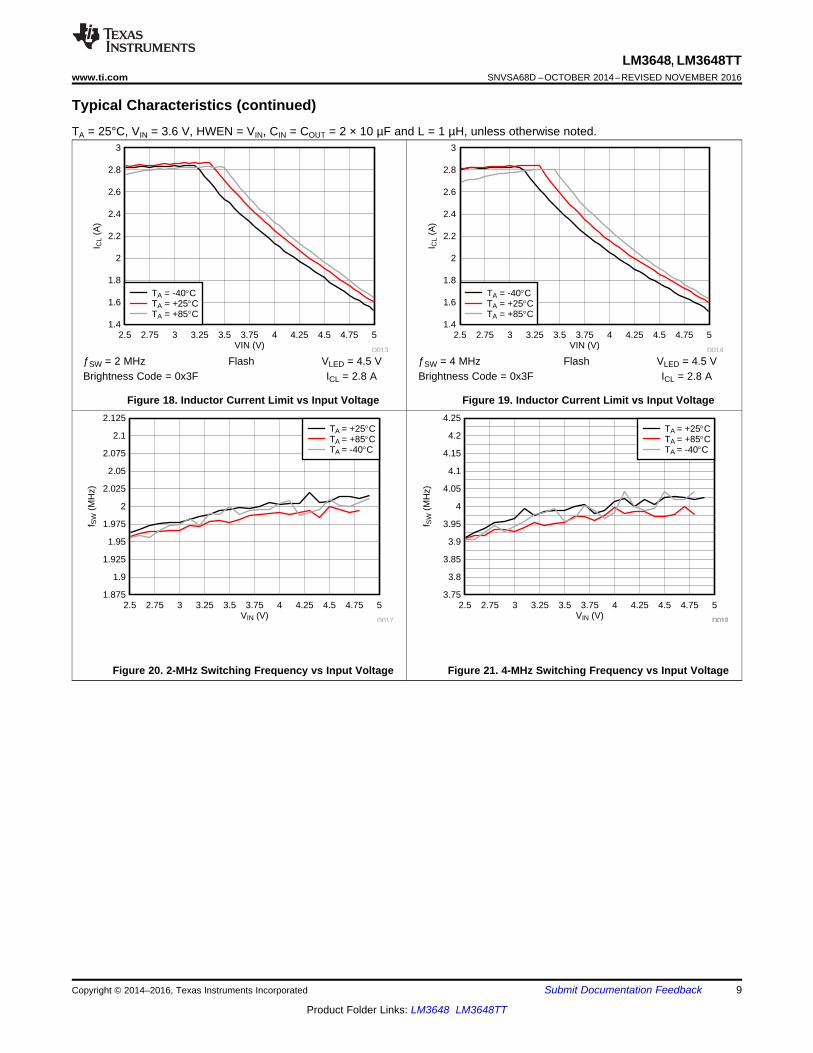
Typical Characteristics (continued)TA = 25°C, VIN = 3.6 V, HWEN = VIN, CIN = COUT = 2 × 10 µF and L = 1 µH, unless otherwise noted.
ƒSW = 2 MHz Flash VLED = 4.5 VBrightness Code = 0x3F ICL = 2.8 A
Figure 18. Inductor Current Limit vs Input Voltage
ƒSW = 4 MHz Flash VLED = 4.5 VBrightness Code = 0x3F ICL = 2.8 A
Figure 19. Inductor Current Limit vs Input Voltage
Figure 20. 2-MHz Switching Frequency vs Input Voltage Figure 21. 4-MHz Switching Frequency vs Input Voltage
10
LM3648, LM3648TTSNVSA68D –OCTOBER 2014–REVISED NOVEMBER 2016 www.ti.com
Product Folder Links: LM3648 LM3648TT
Submit Documentation Feedback Copyright © 2014–2016, Texas Instruments Incorporated
7 Detailed Description
7.1 OverviewThe LM3648 is a high-power white LED flash driver capable of delivering up to 1.5 A to the LED. The deviceincorporates a 2-MHz or 4-MHz constant frequency-synchronous current-mode PWM boost converter and a high-side current source to regulate the LED current over the 2.5-V to 5.5-V input voltage range.
The LM3648 PWM DC/DC boost converter switches and boosts the output to maintain at least VHR across thecurrent source. This minimum headroom voltage ensures that the current source remains in regulation. If theinput voltage is above the LED voltage + current source headroom voltage the device does not switch, but turnsthe PFET on continuously (Pass mode). In Pass mode the difference between (VIN − ILED × RPMOS) and thevoltage across the LED is dropped across the current source.
The LM3648 has three logic inputs including a hardware Flash Enable (STROBE), a hardware Torch Enable(TORCH/TEMP, TORCH = default), and a Flash Interrupt input (TX) designed to interrupt the flash pulse duringhigh battery-current conditions. These logic inputs have internal 300-kΩ (typical) pulldown resistors to GND.
Additional features of the LM3648 include an internal comparator for LED thermal sensing via an external NTCthermistor and an input voltage monitor that can reduce the Flash current during low VIN conditions. It also has aHardware Enable (HWEN) pin that can be used to reset the state of the device and the registers by pulling theHWEN pin to ground.
Control is done via an I2C-compatible interface. This includes adjustment of the Flash and Torch current levels,changing the Flash Timeout Duration, and changing the switch current limit. Additionally, there are flag andstatus bits that indicate flash current time-out, LED overtemperature condition, LED failure (open/short), devicethermal shutdown, TX interrupt, and VIN undervoltage conditions.

+-
VOVP
PWM Control
ThermalShutdown
+150oC
INVREF
I2C
Interface
+
-
+ -
ErrorAmplifier
SlopeCompensation
SDA
SCL
ControlLogic/
Registers
GND
OUT
LED
TORCH/TEMP
TXSTROBEENABLE
SW
65 m:
86 m:
Over Voltage Comparator
+-
NTC VTRIP
INTC
ILED
Soft-Start
+-
2/4 MHzOscillator
+-
UVLOInput Voltage Flash Monitor
OUT-VHR
Current Sense/Current Limit
11
LM3648, LM3648TTwww.ti.com SNVSA68D –OCTOBER 2014–REVISED NOVEMBER 2016
Product Folder Links: LM3648 LM3648TT
Submit Documentation FeedbackCopyright © 2014–2016, Texas Instruments Incorporated
7.2 Functional Block Diagram
7.3 Feature Description
7.3.1 Flash ModeIn Flash Mode, the LED current source (LED) provides 64 target current levels from 21.8 mA to 1500 mA. Oncethe Flash sequence is activated the current source (LED) ramps up to the programmed Flash current by steppingthrough all current steps until the programmed current is reached. The headroom in the current source can beregulated to provide 21.8 mA to 1.5 A.
When the device is enabled in Flash Mode through the Enable Register, all mode bits in the Enable Register arecleared after a flash time-out event.

M1
,M0
= Z
01[
ST
RO
BE
EN
= Z
1[
VOUT
STROBE
ILED
M1
,M0
= Z
00[
EN
= Z
1[
VOUT
STROBE
ILED
OFF
PASS
BOOST
M1
,M0
= Z
01[
ST
RO
BE
EN
= Z
1[
M1
,M0
= Z
00[
ST
RO
BE
EN
= Z
1[
12
LM3648, LM3648TTSNVSA68D –OCTOBER 2014–REVISED NOVEMBER 2016 www.ti.com
Product Folder Links: LM3648 LM3648TT
Submit Documentation Feedback Copyright © 2014–2016, Texas Instruments Incorporated
Feature Description (continued)7.3.2 Torch ModeIn Torch mode, the LED current source (LED) provide 128 target current levels from 1.954 mA to 358 mA or3.908 mA to 502.308 mA on LM3648TT. The Torch current is adjusted via the LED Torch Brightness Register.Torch mode is activated by the Enable Register (setting M1, M0 to '10'), or by pulling the TORCH/TEMP pinHIGH when the pin is enabled (Enable Register) and set to Torch Mode. Once the TORCH sequence is activatedthe active current source (LED) ramps up to the programmed Torch current by stepping through all current stepsuntil the programmed current is reached. The rate at which the current ramps is determined by the value chosenin the Timing Register.
Torch Mode is not affected by Flash Timeout or by a TX Interrupt event.
7.3.3 IR ModeIn IR Mode, the target LED current is equal to the value stored in the LED Flash Brightness Registers. When IRmode is enabled (setting M1, M0 to '01'), the boost converter turns on and sets the output equal to the input(pass-mode). At this point, toggling the STROBE pin enables and disables the LED current source (if enabled).The STROBE pin can only be set to be Level sensitive, meaning all timing of the IR pulse is externally controlled.In IR Mode, the current source does not ramp the LED output to the target. The current transitions immediatelyfrom off to on and then on to off.
Figure 22. IR Mode with Boost
Figure 23. IR Mode Pass Only

VOUT
STROBE
ILED
TIM
E-O
UT
Sta
rt
TIM
E-O
UT
Sta
rt
TIM
E-O
UT
Sta
rt
TIM
E-O
UT
RE
SE
T
TIM
E-O
UT
RE
SE
T
TIM
E-O
UT
Re
ach
ed
VO
UT
go
es
low
, LE
D t
urn
off
M1
,M0
= Z
01[
ST
RO
BE
EN
= Z
1[
13
LM3648, LM3648TTwww.ti.com SNVSA68D –OCTOBER 2014–REVISED NOVEMBER 2016
Product Folder Links: LM3648 LM3648TT
Submit Documentation FeedbackCopyright © 2014–2016, Texas Instruments Incorporated
Feature Description (continued)
Figure 24. IR Mode Timeout
7.4 Device Functioning Modes
7.4.1 Start-Up (Enabling The Device)Turnon of the LM3648 Torch and Flash modes can be done through the Enable Register. On start-up, whenVOUT is less than VIN the internal synchronous PFET turns on as a current source and delivers 200 mA (typ.) tothe output capacitor. During this time the current source (LED) is off. When the voltage across the outputcapacitor reaches 2.2 V (typ.), the current source turns on. At turnon the current source steps through eachFLASH or TORCH level until the target LED current is reached. This gives the device a controlled turnon andlimits inrush current from the VIN supply.
7.4.2 Pass ModeThe LM3648 starts up in Pass Mode and stays there until Boost Mode is needed to maintain regulation. If thevoltage difference between VOUT and VLED falls below VHR, the device switches to Boost Mode. In Pass Mode theboost converter does not switch, and the synchronous PFET turns fully on bringing VOUT up to VIN − ILED ×RPMOS. In Pass Mode the inductor current is not limited by the peak current limit.
7.4.3 Power Amplifier Synchronization (TX)The TX pin is a Power Amplifier Synchronization input. This is designed to reduce the flash LED current and thuslimit the battery current during high battery current conditions such as PA transmit events. When the LM3648 isengaged in a Flash event, and the TX pin is pulled high, the LED current is forced into Torch Mode at theprogrammed Torch current setting. If the TX pin is then pulled low before the Flash pulse terminates, the LEDcurrent returns to the previous Flash current level. At the end of the Flash time-out, whether the TX pin is high orlow, the LED current turns off.
7.4.4 Input Voltage Flash Monitor (IVFM)The LM3648 has the ability to adjust the flash current based upon the voltage level present at the IN pin utilizingthe Input Voltage Flash Monitor (IVFM). The adjustable threshold IVFM-D ranges from 2.9 V to 3.6 V in 100-mVsteps, with three different usage modes (Stop and Hold, Adjust Down Only, Adjust Up and Down). The Flags2Register has the IVFM flag bit set when the input voltage crosses the IVFM-D value. Additionally, the IVFM-Dthreshold sets the input voltage boundary that forces the LM3648 to either stop ramping the flash current duringstart-up (Stop and Hold Mode) or to start decreasing the LED current during the flash (Down Adjust Only and Upand Down Adjust). In Adjust Up and Down mode, the IVFM-D value plus the hysteresis voltage threshold set theinput voltage boundary that forces the LM3648 to start ramping the flash current back up towards the target.

IVFM ENABLE
LEVEL STROBE
VIN PROFILE for Stop and Hold Mode
O/P Current
Profile in Stop
and Hold Mode
Dotted line shows O/P Current
Profile with IVFM Disabled
Set Target Flash Current
IVFM-D
T-F
ilte
r =
4P
s
VIN PROFILE for Down Mode
IVFM-DHysteresis
SET RAMP FROM
THE RAMP
REGISTER USED
T-F
ilte
r =
4P
s
O/P Current Profile
in Down Mode
VIN PROFILE for Up/ Down Mode
O/P Current Profile
in Up and Down
Mode
IVFM-DHysteresis
14
LM3648, LM3648TTSNVSA68D –OCTOBER 2014–REVISED NOVEMBER 2016 www.ti.com
Product Folder Links: LM3648 LM3648TT
Submit Documentation Feedback Copyright © 2014–2016, Texas Instruments Incorporated
Device Functioning Modes (continued)
Figure 25. IVFM Modes

VIN
VTRIPControlLogic
NTC Control Block
TEMPINTC
NTC +-
15
LM3648, LM3648TTwww.ti.com SNVSA68D –OCTOBER 2014–REVISED NOVEMBER 2016
Product Folder Links: LM3648 LM3648TT
Submit Documentation FeedbackCopyright © 2014–2016, Texas Instruments Incorporated
Device Functioning Modes (continued)7.4.5 Fault/Protections
7.4.5.1 Fault OperationIf the LM3648 enters a fault condition, the device sets the appropriate flag in the Flags1 and Flags2 Registers(0x0A and 0x0B), and places the device into standby by clearing the Mode Bits ([1],[0]) in the Enable Register.The LM3648 remains in standby until an I2C read of the Flags1 and Flags2 Registers are completed. Uponclearing the flags/faults, the device can be restarted (Flash, Torch, IR, etc.). If the fault is still present, theLM3648 re-enters the fault state and enters standby again.
7.4.5.2 Flash Time-OutThe Flash Time-Out period sets the amount of time that the Flash Current is being sourced from the currentsource (LED). The LM3648 has 16 timeout levels ranging from 10 ms to 400 ms or 40 ms (see TimingConfiguration Register (0x08) for more detail).
7.4.5.3 Overvoltage Protection (OVP)The output voltage is limited to typically 5 V (see VOVP spec in the Electrical Characteristics). In situations suchas an open LED, the LM3648 raises the output voltage in order to keep the LED current at its target value. WhenVOUT reaches 5 V (typical), the overvoltage comparator trips and turns off the internal NFET. When VOUT fallsbelow the “VOVP Off Threshold”, the LM3648 begins switching again. The mode bits are cleared, and the OVPflag is set, when an OVP condition is present for three rising OVP edges. This prevents momentary OVP eventsfrom forcing the device to shut down.
7.4.5.4 Current LimitThe LM3648 features two selectable inductor current limits that are programmable through the I2C-compatibleinterface. When the inductor current limit is reached, the LM3648 terminates the charging phase of the switchingcycle. Switching resumes at the start of the next switching period. If the overcurrent condition persists, the deviceoperates continuously in current limit.
Because the current limit is sensed in the NMOS switch, there is no mechanism to limit the current when thedevice operates in Pass Mode (current does not flow through the NMOS in pass mode). In Boost mode or Passmode if VOUT falls below 2.3 V, the device stops switching, and the PFET operates as a current source limitingthe current to 200 mA. This prevents damage to the LM3648 and excessive current draw from the battery duringoutput short-circuit conditions. The mode bits are not cleared upon a Current Limit event, but a flag is set.
7.4.5.5 NTC Thermistor Input (Torch/Temp)The TORCH/TEMP pin, when set to TEMP mode, serves as a threshold detector and bias source for negativetemperature coefficient (NTC) thermistors. When the voltage at TEMP goes below the programmed threshold,the LM3648 is placed into standby mode. The NTC threshold voltage is adjustable from 200 mV to 900 mV in100-mV steps. The NTC bias current is set to 50 µA. The NTC detection circuitry can be enabled or disabled viathe Enable Register. If enabled, the NTC block turns on and off during the start and stop of a Flash/Torch event.
Additionally, the NTC input looks for an open NTC connection and a shorted NTC connection. If the NTC inputfalls below 100 mV, the NTC short flag is set, and the device is disabled. If the NTC input rises above 2.3 V, theNTC Open flag is set, and the device is disabled. These fault detections can be individually disabled/enabled viathe NTC Open Fault Enable bit and the NTC Short Fault Enable bit.
Figure 26. Temp Detection Diagram
16
LM3648, LM3648TTSNVSA68D –OCTOBER 2014–REVISED NOVEMBER 2016 www.ti.com
Product Folder Links: LM3648 LM3648TT
Submit Documentation Feedback Copyright © 2014–2016, Texas Instruments Incorporated
Device Functioning Modes (continued)7.4.5.6 Undervoltage Lockout (UVLO)The LM3648 has an internal comparator that monitors the voltage at IN and forces the LM3648 into standby ifthe input voltage drops to 2.5 V. If the UVLO monitor threshold is tripped, the UVLO flag bit is set in the Flags1Register (0x0A). If the input voltage rises above 2.5 V, the LM3648 is not available for operation until there is anI2C read of the Flags1 Register (0x0A). Upon a read, the Flags1 register is cleared, and normal operation canresume if the input voltage is greater than 2.5 V.
7.4.5.7 Thermal Shutdown (TSD)When the LM3648 die temperature reaches 150°C, the thermal shutdown detection circuit trips, forcing theLM3648 into standby and writing a '1' to the corresponding bit of the Flags1 Register (0x0A) (Thermal Shutdownbit). The LM3648 is only allowed to restart after the Flags1 Register (0x0A) is read, clearing the fault flag. Uponrestart, if the die temperature is still above 150°C, the LM3648 resets the Fault flag and re-enters standby.
7.4.5.8 LED and/or VOUT Short FaultThe LED Fault flags read back a '1' if the device is active in Flash or Torch mode and the LED outputexperiences a short condition. The Output Short Fault flag reads back a '1' if the device is active in Flash orTorch mode and the boost output experiences a short condition. An LED short condition is determined if thevoltage at LED goes below 500 mV (typ.) while the device is in Torch or Flash mode. There is a deglitch time of256 μs before the LED Short flag is valid, and a deglitch time of 2.048 ms before the VOUT Short flag is valid.The LED Short Faults can be reset to '0' by removing power to the LM3648, setting HWEN to '0', setting the SWRESET bit to a '1', or by reading back the Flags1 Register (0x0A on LM3648). The mode bits are cleared uponan LED and/or VOUT short fault.
7.5 Programming
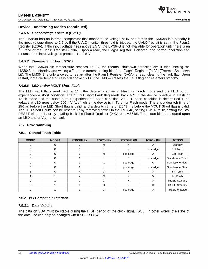
7.5.1 Control Truth Table
MODE1 MODE0 STROBE EN TORCH EN STROBE PIN TORCH PIN ACTION0 0 0 0 X X Standby0 0 0 1 X pos edge Ext Torch0 0 1 0 pos edge X Ext Flash0 0 1 1 0 pos edge Standalone Torch0 0 1 1 pos edge 0 Standalone Flash0 0 1 1 pos edge pos edge Standalone Flash1 0 X X X X Int Torch1 1 X X X X Int Flash0 1 0 X X X IRLED Standby0 1 1 X 0 X IRLED Standby0 1 1 X pos edge X IRLED enabled
7.5.2 I2C-Compatible Interface
7.5.2.1 Data ValidityThe data on SDA must be stable during the HIGH period of the clock signal (SCL). In other words, the state ofthe data line can only be changed when SCL is LOW.
start msb Chip Address lsb w ack msb Register Add lsb ack msb DATA lsb ack stop
ack from slave ack from slave ack from slave
SCL
SDA
start Id = 63h w ack addr = 0Ah ack ackData = 03h stop
SDA
Start Condition Stop Condition
SCLS P
SCL
SDA
data change allowed
data valid
data change allowed
data valid
data change allowed
17
LM3648, LM3648TTwww.ti.com SNVSA68D –OCTOBER 2014–REVISED NOVEMBER 2016
Product Folder Links: LM3648 LM3648TT
Submit Documentation FeedbackCopyright © 2014–2016, Texas Instruments Incorporated
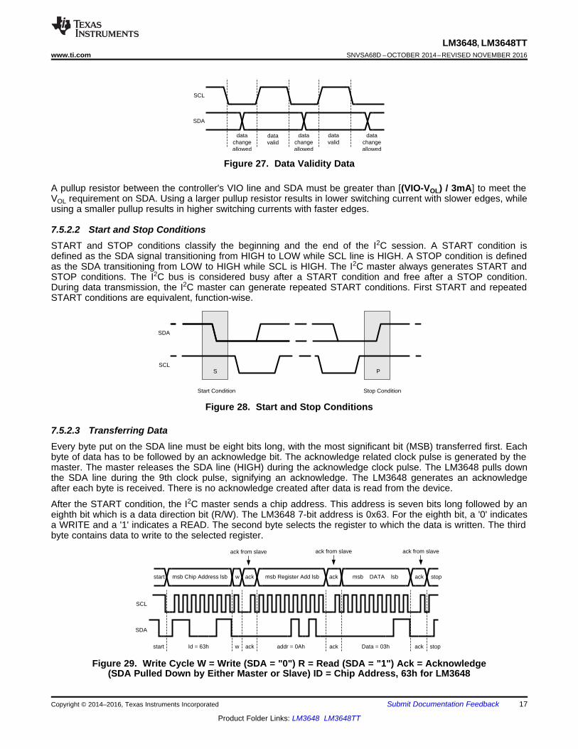
Figure 27. Data Validity Data
A pullup resistor between the controller's VIO line and SDA must be greater than [(VIO-VOL) / 3mA] to meet theVOL requirement on SDA. Using a larger pullup resistor results in lower switching current with slower edges, whileusing a smaller pullup results in higher switching currents with faster edges.
7.5.2.2 Start and Stop ConditionsSTART and STOP conditions classify the beginning and the end of the I2C session. A START condition isdefined as the SDA signal transitioning from HIGH to LOW while SCL line is HIGH. A STOP condition is definedas the SDA transitioning from LOW to HIGH while SCL is HIGH. The I2C master always generates START andSTOP conditions. The I2C bus is considered busy after a START condition and free after a STOP condition.During data transmission, the I2C master can generate repeated START conditions. First START and repeatedSTART conditions are equivalent, function-wise.
Figure 28. Start and Stop Conditions
7.5.2.3 Transferring DataEvery byte put on the SDA line must be eight bits long, with the most significant bit (MSB) transferred first. Eachbyte of data has to be followed by an acknowledge bit. The acknowledge related clock pulse is generated by themaster. The master releases the SDA line (HIGH) during the acknowledge clock pulse. The LM3648 pulls downthe SDA line during the 9th clock pulse, signifying an acknowledge. The LM3648 generates an acknowledgeafter each byte is received. There is no acknowledge created after data is read from the device.
After the START condition, the I2C master sends a chip address. This address is seven bits long followed by aneighth bit which is a data direction bit (R/W). The LM3648 7-bit address is 0x63. For the eighth bit, a '0' indicatesa WRITE and a '1' indicates a READ. The second byte selects the register to which the data is written. The thirdbyte contains data to write to the selected register.
Figure 29. Write Cycle W = Write (SDA = "0") R = Read (SDA = "1") Ack = Acknowledge(SDA Pulled Down by Either Master or Slave) ID = Chip Address, 63h for LM3648

R/WBit 0
1Bit 1
1Bit 2
0Bit 3
0Bit 4
0Bit 5
1Bit 7
1Bit 6
MSB LSB
I2C Slave Address (chip address)
18
LM3648, LM3648TTSNVSA68D –OCTOBER 2014–REVISED NOVEMBER 2016 www.ti.com
Product Folder Links: LM3648 LM3648TT
Submit Documentation Feedback Copyright © 2014–2016, Texas Instruments Incorporated
7.5.2.4 I2C-Compatible Chip AddressThe device address for the LM3648 is 1100011 (0x63). After the START condition, the I2C-compatible mastersends the 7-bit address followed by an eighth read or write bit (R/W). R/W = 0 indicates a WRITE and R/W = 1indicates a READ. The second byte following the device address selects the register address to which the data iswritten. The third byte contains the data for the selected register.
Figure 30. I2C-Compatible Chip Address
7.6 Register Descriptions
REGISTER NAME INTERNAL HEX ADDRESSPOWER ON/RESET VALUE
LM3648Enable Register 0x01 0x80IVFM Register 0x02 0x01LED Flash Brightness Register 0x03 0xBFLED Torch Brightness Register 0x05 0xBFBoost Configuration Register 0x07 0x09Timing Configuration Register 0x08 0x1ATEMP Register 0x09 0x08Flags1 Register 0x0A 0x00Flags2 Register 0x0B 0x00Device ID Register 0x0C 0x02 or 0x04 for LM3648TTLast Flash Register 0x0D 0x00
19
LM3648, LM3648TTwww.ti.com SNVSA68D –OCTOBER 2014–REVISED NOVEMBER 2016
Product Folder Links: LM3648 LM3648TT
Submit Documentation FeedbackCopyright © 2014–2016, Texas Instruments Incorporated
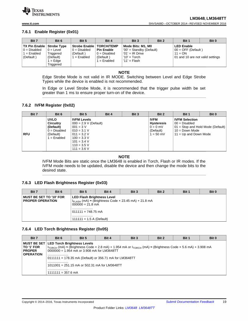
7.6.1 Enable Register (0x01)
Bit 7 Bit 6 Bit 5 Bit 4 Bit 3 Bit 2 Bit 1 Bit 0TX Pin Enable0 = Disabled1 = Enabled(Default )
Strobe Type0 = LevelTriggered(Default)1 = EdgeTriggered
Strobe Enable0 = Disabled(Default )1 = Enabled
TORCH/TEMPPin Enable0 = Disabled(Default )1 = Enabled
Mode Bits: M1, M0'00' = Standby (Default)'01' = IR Drive'10' = Torch'11' = Flash
LED Enable00 = OFF (Default )11 = ON01 and 10 are not valid settings
NOTEEdge Strobe Mode is not valid in IR MODE. Switching between Level and Edge StrobeTypes while the device is enabled is not recommended.
In Edge or Level Strobe Mode, it is recommended that the trigger pulse width be setgreater than 1 ms to ensure proper turn-on of the device.
7.6.2 IVFM Register (0x02)
Bit 7 Bit 6 Bit 5 Bit 4 Bit 3 Bit 2 Bit 1 Bit 0
RFU
UVLOCircuitry(Default)0 = Disabled(Default)1 = Enabled
IVFM Levels000 = 2.9 V (Default)001 = 3 V010 = 3.1 V011 = 3.2 V100 = 3.3 V101 = 3.4 V110 = 3.5 V111 = 3.6 V
IVFMHysteresis0 = 0 mV(Default)1 = 50 mV
IVFM Selection00 = Disabled01 = Stop and Hold Mode (Default)10 = Down Mode11 = Up and Down Mode
NOTEIVFM Mode Bits are static once the LM3648 is enabled in Torch, Flash or IR modes. If theIVFM mode needs to be updated, disable the device and then change the mode bits to thedesired state.
7.6.3 LED Flash Brightness Register (0x03)
Bit 7 Bit 6 Bit 5 Bit 4 Bit 3 Bit 2 Bit 1 Bit 0MUST BE SET TO '10' FORPROPER OPERATION
LED Flash Brightness LevelIFLASH (mA) ≈ (Brightness Code × 23.45 mA) + 21.8 mA000000 = 21.8 mA.......................011111 = 748.75 mA.......................111111 = 1.5 A (Default)
7.6.4 LED Torch Brightness Register (0x05)
Bit 7 Bit 6 Bit 5 Bit 4 Bit 3 Bit 2 Bit 1 Bit 0MUST BE SETTO '1' FORPROPEROPERATION
LED Torch Brightness LevelsITORCH (mA) ≈ (Brightness Code × 2.8 mA) + 1.954 mA or ITORCH (mA) ≈ (Brightness Code × 5.6 mA) + 3.908 mA0000000 = 1.954 mA or 3.908 mA for LM3648TT.......................0111111 = 178.35 mA (Default) or 356.71 mA for LM3648TT.......................1011001 = 251.15 mA or 502.31 mA for LM3648TT.......................1111111 = 357.6 mA

20
LM3648, LM3648TTSNVSA68D –OCTOBER 2014–REVISED NOVEMBER 2016 www.ti.com
Product Folder Links: LM3648 LM3648TT
Submit Documentation Feedback Copyright © 2014–2016, Texas Instruments Incorporated
NOTEMaximum Torch Brightness Code allowed for the LM3648TT is 0x59 (1011001), whichresults in 502.31 mA current setting. Higher settings may result in over-heating andpotentially damaging the device.
7.6.5 Boost Configuration Register (0x07)
Bit 7 Bit 6 Bit 5 Bit 4 Bit 3 Bit 2 Bit 1 Bit 0
SoftwareReset Bit
0 = Not Reset(Default)1 = Reset
RFU RFU RFU
LED Pin ShortFault Detect0 = Disabled1 = Enabled(Default)
Boost Mode0 = Normal(Default)1 = Pass ModeOnly
BoostFrequencySelect0 = 2 MHz(Default)1 = 4 MHz
Boost CurrentLimit Setting0 = 1.9 A1 = 2.8 A(Default)
7.6.6 Timing Configuration Register (0x08)
Bit 7 Bit 6 Bit 5 Bit 4 Bit 3 Bit 2 Bit 1 Bit 0
RFU
Torch Current Ramp Time000 = No Ramp001 = 1 ms (Default)010 = 32 ms011 = 64 ms100 = 128 ms101 = 256 ms110 = 512 ms111 = 1024 ms
Flash Time-Out Duration0000 = 10 ms or 40 ms (LM3648TT)0001 = 20 ms or 80 ms (LM3648TT)0010 = 30 ms or 120 ms (LM3648TT)0011 = 40 ms or 160 ms (LM3648TT)0100 = 50 ms or 200 ms (LM3648TT)0101 = 60 ms or 240 ms (LM3648TT)0110 = 70 ms or 280 ms (LM3648TT)0111 = 80 ms or 320 ms (LM3648TT)1000 = 90 ms or 360 ms (LM3648TT)1001 = 100 ms or 400 ms (LM3648TT)1010 = 150 ms (Default) or 600 ms (LM3648TT)1011 = 200 ms or 800 ms (LM3648TT)1100 = 250 ms or 1000 ms (LM3648TT)1101 = 300 ms or 1200 ms (LM3648TT)1110 = 350 ms or 1400 ms (LM3648TT)1111 = 400 ms or 1600 ms (LM3648TT)
NOTEOn the LM3648TT, special care must be taken with regards to thermal management whenusing time-out values greater than 400 ms. Depending on the PCB layout, input voltage,and output current, it is possible to have the internal thermal shutdown circuit trip prior toreaching the desired flash time-out value.
7.6.7 TEMP Register (0x09)
Bit 7 Bit 6 Bit 5 Bit 4 Bit 3 Bit 2 Bit 1 Bit 0
RFU
TORCHPolarity0 = ActiveHigh (Default)(PulldownResistorEnabled)1 = Active Low(PulldownResistorDisabled)
NTC OpenFault Enable0 = Disabled(Default)1 =Enable
NTC ShortFault Enable0 = Disabled(Default)1 =Enable
TEMP Detect Voltage Threshold000 = 0.2 V001 = 0.3 V010 = 0.4 V011 = 0.5 V100 = 0.6 V (Default)101 = 0.7 V110 = 0.8 V111 = 0.9 V
TORCH/TEMPFunctionSelect0 = TORCH(Default)1 = TEMP
NOTEThe Torch Polarity bit is static once the LM3648 is enabled in Torch, Flash, or IR modes.If the Torch Polarity bit needs to be updated, disable the device and then change theTorch Polarity bit to the desired state.

21
LM3648, LM3648TTwww.ti.com SNVSA68D –OCTOBER 2014–REVISED NOVEMBER 2016
Product Folder Links: LM3648 LM3648TT
Submit Documentation FeedbackCopyright © 2014–2016, Texas Instruments Incorporated
7.6.8 Flags1 Register (0x0A)
Bit 7 Bit 6 Bit 5 Bit 4 Bit 3 Bit 2 Bit 1 Bit 0
TX Flag VOUT ShortFault
VLED ShortFault
VLED ShortFault
Current LimitFlag
ThermalShutdown(TSD) Fault
UVLO Fault Flash Time-OutFlag
7.6.9 Flags2 Register (0x0B)
Bit 7 Bit 6 Bit 5 Bit 4 Bit 3 Bit 2 Bit 1 Bit 0
RFU RFU RFU NTC ShortFault NTC Open Fault IVFM Trip
Flag OVP Fault TEMP TripFault
7.6.10 Device ID Register (0x0C)
Bit 7 Bit 6 Bit 5 Bit 4 Bit 3 Bit 2 Bit 1 Bit 0
RFU RFU Device ID'000'
Silicon Revision Bits'010' or '100' for LM3648TT
7.6.11 Last Flash Register (0x0D)
Bit 7 Bit 6 Bit 5 Bit 4 Bit 3 Bit 2 Bit 1 Bit 0RFU The value stored is always the last current value the IVFM detection block set. ILED = IFLASH-TARGET × ((Code + 1) / 128)

IN
HWEN
LM3648
SDA
SCL
SW
OUT
LED
STROBE
TORCH/TEMP
GNDTX
10 PF
10 PF
C2
L1
C1
PP/PC
VIN
2.5V t 5.5V
1 PH
22
LM3648, LM3648TTSNVSA68D –OCTOBER 2014–REVISED NOVEMBER 2016 www.ti.com
Product Folder Links: LM3648 LM3648TT
Submit Documentation Feedback Copyright © 2014–2016, Texas Instruments Incorporated
8 Applications and Implementation
NOTEInformation in the following applications sections is not part of the TI componentspecification, and TI does not warrant its accuracy or completeness. TI’s customers areresponsible for determining suitability of components for their purposes. Customers shouldvalidate and test their design implementation to confirm system functionality.
8.1 Application InformationThe LM3648 can drive a flash LED at currents up to 1.5 A. The 2-MHz or 4-MHz DC-DC boost regulator allowsfor the use of small value discrete external components.
8.2 Typical Application
Figure 31. LM3648 Typical Application
8.2.1 Design RequirementsExample requirements based on default register values:
Table 1. Design ParametersDESIGN PARAMETER EXAMPLE VALUE
Input Voltage Range 2.5 V to 5.5 VBrightness Control I2C RegisterLED Configuration 1 Flash LED
Boost Switching Frequency 2 MHz (4 MHz selectable)Flash Brightness 1.5-A Max Current
where IN INOUT
( )- VVxVL =I'
OUTSW VxLxfx2
I+xR=V LESRESR ''VxI OUTLED
VIN ¹·
©§
Q =V'( )INOUTLED - VVxI
OUTOUTSW CxVxf
23
LM3648, LM3648TTwww.ti.com SNVSA68D –OCTOBER 2014–REVISED NOVEMBER 2016
Product Folder Links: LM3648 LM3648TT
Submit Documentation FeedbackCopyright © 2014–2016, Texas Instruments Incorporated
8.2.2 Detailed Design Procedure
8.2.2.1 Output Capacitor SelectionThe LM3648 is designed to operate with a 10-µF ceramic output capacitor. When the boost converter is running,the output capacitor supplies the load current during the boost converter on-time. When the NMOS switch turnsoff, the inductor energy is discharged through the internal PMOS switch, supplying power to the load andrestoring charge to the output capacitor. This causes a sag in the output voltage during the on-time and a rise inthe output voltage during the off-time. The output capacitor is therefore chosen to limit the output ripple to anacceptable level depending on load current and input or output voltage differentials and also to ensure theconverter remains stable.
Larger capacitors such as a 22-µF or capacitors in parallel can be used if lower output voltage ripple is desired.To estimate the output voltage ripple considering the ripple due to capacitor discharge (ΔVQ) and the ripple dueto the capacitors ESR (ΔVESR) use the following equations:
For continuous conduction mode, the output voltage ripple due to the capacitor discharge is:
(1)
The output voltage ripple due to the output capacitors ESR is found by:
(2)
In ceramic capacitors the ESR is very low so the assumption is that 80% of the output voltage ripple is due tocapacitor discharge and 20% from ESR. Table 2 lists different manufacturers for various output capacitors andtheir case sizes suitable for use with the LM3648.
8.2.2.2 Input Capacitor SelectionChoosing the correct size and type of input capacitor helps minimize the voltage ripple caused by the switchingof the LM3648 boost converter and reduce noise on the boost converter's input pin that can feed through anddisrupt internal analog signals. In the typical application circuit a 10-µF ceramic input capacitor works well. It isimportant to place the input capacitor as close as possible to the LM3648 input (IN) pin. This reduces the seriesresistance and inductance that can inject noise into the device due to the input switching currents. Table 2 listsvarious input capacitors recommended for use with the LM3648.
Table 2. Recommended Input/Output Capacitors (X5R/X7R Dielectric)MANUFACTURER PART NUMBER VALUE CASE SIZE VOLTAGE RATING
TDK Corporation C1608JB0J106M 10 µF 0603 (1.6 mm × 0.8 mm × 0.8 mm) 6.3 VTDK Corporation C2012JB1A106M 10 µF 0805 (2.0 mm × 1.25 mm × 1.25 mm) 10 VMurata GRM188R60J106M 10 µF 0603 (1.6 mm × 0.8 mm × 0.8 mm) 6.3 VMurata GRM21BR61A106KE19 10 µF 0805 (2.0 mm × 1.25 mm × 1.25 mm) 10 V
8.2.2.3 Inductor SelectionThe LM3648 is designed to use a 0.47-µH or 1-µH inductor. Table 3 lists various inductors and theirmanufacturers that work well with the LM3648. When the device is boosting (VOUT > VIN) the inductor is typicallythe largest area of efficiency loss in the circuit. Therefore, choosing an inductor with the lowest possible seriesresistance is important. Additionally, the saturation rating of the inductor must be greater than the maximumoperating peak current of the LM3648. This prevents excess efficiency loss that can occur with inductors thatoperate in saturation. For proper inductor operation and circuit performance, ensure that the inductor saturationand the peak current limit setting of the LM3648 are greater than IPEAK in Equation 3:

VIN (V)
KLE
D (
%)
2.5 3 3.5 4 4.5 5 5.560
64
68
72
76
80
84
88
92
96
100
D028
TA = -40qCTA = +25qCTA = +85qC
VIN (V)
KLE
D (
%)
2.5 3 3.5 4 4.5 5 5.560
64
68
72
76
80
84
88
92
96
100
D029
TA = -40qCTA = +25qCTA = +85qC
VIN (V)
KLE
D (
%)
2.5 3 3.5 4 4.5 5 5.550
55
60
65
70
75
80
85
90
95
100
D019
VLED = 3.0VVLED = 3.2VVLED = 3.5VVLED = 3.8VVLED = 4.1VVLED = 4.4V
VIN (V)
KLE
D (
%)
2.5 3 3.5 4 4.5 5 5.550
55
60
65
70
75
80
85
90
95
100
D020
VLED = 3.0VVLED = 3.2VVLED = 3.5VVLED = 3.8VVLED = 4.1VVLED = 4.4V
PEAKI LOADI=
Kx LI+' where L =I' IN xV ( )INOUT - VV
OUTSW VxLxfx2IN
OUT
V
V
24
LM3648, LM3648TTSNVSA68D –OCTOBER 2014–REVISED NOVEMBER 2016 www.ti.com
Product Folder Links: LM3648 LM3648TT
Submit Documentation Feedback Copyright © 2014–2016, Texas Instruments Incorporated
where• ƒSW = 2 or 4 MHz (3)
Efficiency details can be found in the Application Curves .
Table 3. Recommended InductorsMANUFACTURER L PART NUMBER DIMENSIONS (L×W×H) ISAT RDC
TOKO 0.47 µH DFE201610P-R470M 2.0 mm x 1.6 mm x 1.0 mm 4.1 A 32 mΩTOKO 1 µH DFE201610P-1R0M 2.0 mm x 1.6 mm x 1.0 mm 3.7 A 58 mΩ
8.2.3 Application CurvesAmbient temperature is 25°C, input voltage is 3.6 V, HWEN = VIN, CIN = 2 × 10 µF, COUT = 2 × 10 µF and L = 1 µH, unlessotherwise noted.
ƒSW = 2 MHz FlashBrightness Code = 0x3F
Figure 32. 2-MHz LED Efficiency vs Input Voltage
ƒSW = 4 MHz FlashBrightness Code = 0x3F
Figure 33. 4-MHz LED Efficiency vs Input Voltage
ƒSW = 2 MHz Flash VLED = 3.55 VBrightness Code = 0x3F
Figure 34. LED Efficiency vs Input Voltage
ƒSW = 4 MHz Flash VLED = 3.55 VBrightness Code = 0x3F
Figure 35. LED Efficiency vs Input Voltage

VIN (V)
KLE
D (
%)
2.5 3 3.5 4 4.5 5 5.550
55
60
65
70
75
80
85
90
95
100
D036
TA = -40qCTA = +25qCTA = +85qC
VIN (V)
KLE
D (
%)
2.5 3 3.5 4 4.5 5 5.550
55
60
65
70
75
80
85
90
95
100
D034
TA = -40CTA = 25CTA = 85C
VIN (V)
KLE
D (
%)
2.5 3 3.5 4 4.5 5 5.550
55
60
65
70
75
80
85
90
95
100
D034
TA = -40qCTA = +25qCTA = +85qC
VIN (V)
KLE
D (
%)
2.5 3 3.5 4 4.5 5 5.550
55
60
65
70
75
80
85
90
95
100
D035
TA = -40qCTA = +25qCTA = +85qC
VIN (V)
KLE
D (
%)
2.5 3 3.5 4 4.5 5 5.560
64
68
72
76
80
84
88
92
96
100
D030
TA = -40qCTA = +25qCTA = +85qC
VIN (V)
KLE
D (
%)
2.5 3 3.5 4 4.5 5 5.550
55
60
65
70
75
80
85
90
95
100
D033
TA = -40qCTA = +25qCTA = +85qC
25
LM3648, LM3648TTwww.ti.com SNVSA68D –OCTOBER 2014–REVISED NOVEMBER 2016
Product Folder Links: LM3648 LM3648TT
Submit Documentation FeedbackCopyright © 2014–2016, Texas Instruments Incorporated
Ambient temperature is 25°C, input voltage is 3.6 V, HWEN = VIN, CIN = 2 × 10 µF, COUT = 2 × 10 µF and L = 1 µH, unlessotherwise noted.
ƒSW = 2 MHz Flash VLED = 3.32 VBrightness Code = 0x2B
Figure 36. LED Efficiency vs Input Voltage
ƒSW = 2 MHz Torch VLED = 2.83 VBrightness Code = 0x3F
Figure 37. LED Efficiency vs Input Voltage
ƒSW = 4 MHz Torch VLED = 2.83 VBrightness Code = 0x3F
Figure 38. LED Efficiency vs Input Voltage
ƒSW = 2 MHz TorchBrightness Code = 0x7F
Figure 39. LED Efficiency vs Input Voltage
ƒSW = 4 MHz Torch VLED = 2.83 VBrightness Code = 0x7F
Figure 40. LED Efficiency vs Input Voltage
LM3648TT ƒSW = 2 MHz TorchBrightness Code = 0x59 VLED = 3.03 V
Figure 41. LED Efficiency vs Input Voltage

Time (400 ns / DIV)
IL (100 mA/DIV)
VOUT (50 mV/DIV)
ILED (20 mA/DIV)
Time (400 ns / DIV)
IL (100 mA/DIV)
VOUT (50 mV/DIV)
ILED (20 mA/DIV)
Time (400 Ps / DIV)
IIN (500 mA/DIV)
VOUT (2 V/DIV)
ILED (500 mA/DIV)
Time (2 ms / DIV)
IIN (1 A/DIV)
VOUT (2 V/DIV)
ILED (500 mA/DIV)
Tx Signal
Time (400 Ps / DIV)
IIN (500 mA/DIV)
VOUT (2 V/DIV)
ILED (500 mA/DIV)
VIN (V)
KLE
D (
%)
2.5 3 3.5 4 4.5 5 5.550
55
60
65
70
75
80
85
90
95
100
D035
TA = -40CTA = 25CTA = 85C
26
LM3648, LM3648TTSNVSA68D –OCTOBER 2014–REVISED NOVEMBER 2016 www.ti.com
Product Folder Links: LM3648 LM3648TT
Submit Documentation Feedback Copyright © 2014–2016, Texas Instruments Incorporated
Ambient temperature is 25°C, input voltage is 3.6 V, HWEN = VIN, CIN = 2 × 10 µF, COUT = 2 × 10 µF and L = 1 µH, unlessotherwise noted.
LM3648TT ƒSW = 4 MHz TorchBrightness Code = 0x59 VLED = 3.03 V
Figure 42. LED Efficiency vs Input Voltage
ƒSW = 2 MHz VLED = 3.18 VBrightness Code = 0x7F
Figure 43. Start-Up
ƒSW = 2 MHz VLED = 3.18 VBrightness Code = 0x7F
Figure 44. Ramp Down
ƒSW = 2 MHz VLED = 3.18 VBrightness Code = 0x7F
Figure 45. TX Interrupt
ƒSW = 2 MHz VLED = 3.18 VBrightness Code = 0x7F
Figure 46. Ripple at 2 MHz
ƒSW = 4 MHz VLED = 3.18 VBrightness Code = 0x7F
Figure 47. Ripple at 4 MHz

27
LM3648, LM3648TTwww.ti.com SNVSA68D –OCTOBER 2014–REVISED NOVEMBER 2016
Product Folder Links: LM3648 LM3648TT
Submit Documentation FeedbackCopyright © 2014–2016, Texas Instruments Incorporated
9 Power Supply Recommendations
The LM3648 is designed to operate from an input voltage supply range between 2.5 V and 5.5 V. This inputsupply must be well regulated and capable to supply the required input current. If the input supply is located farfrom the LM3648 additional bulk capacitance may be required in addition to the ceramic bypass capacitors.
10 Layout
10.1 Layout GuidelinesThe high switching frequency and large switching currents of the LM3648 make the choice of layout important.The following steps are to be used as a reference to ensure the device is stable and maintains proper LEDcurrent regulation across its intended operating voltage and current range.1. Place CIN on the top layer (same layer as the LM3648) and as close as possible to the device. The input
capacitor conducts the driver currents during the low-side MOSFET turnon and turnoff and can detect currentspikes over 1 A in amplitude. Connecting the input capacitor through short, wide traces to both the IN andGND pins reduces the inductive voltage spikes that occur during switching which can corrupt the VIN line.
2. Place COUT on the top layer (same layer as the LM3648) and as close as possible to the OUT and GND pins.The returns for both CIN and COUT must come together at one point, as close as possible to the GND pin.Connecting COUT through short, wide traces reduce the series inductance on the OUT and GND pins that cancorrupt the VOUT and GND lines and cause excessive noise in the device and surrounding circuitry.
3. Connect the inductor on the top layer close to the SW pin. There must be a low-impedance connection fromthe inductor to SW due to the large DC inductor current, and at the same time the area occupied by the SWnode must be small so as to reduce the capacitive coupling of the high dV/dT present at SW that can coupleinto nearby traces.
4. Avoid routing logic traces near the SW node so as to avoid any capacitively coupled voltages from SW ontoany high-impedance logic lines such as TORCH/TEMP, STROBE, HWEN, SDA, and SCL. A good approachis to insert an inner layer GND plane underneath the SW node and between any nearby routed traces. Thiscreates a shield from the electric field generated at SW.
5. Terminate the flash LED cathode directly to the GND pin of the LM3648. If possible, route the LED returnwith a dedicated path so as to keep the high amplitude LED current out of the GND plane. For a flash LEDthat is routed relatively far away from the LM3648, a good approach is to sandwich the forward and returncurrent paths over the top of each other on two layers. This helps reduce the inductance of the LED currentpath.

GND IN
SW STROBE SCL
SDA
HWENOUTTORCH/TEMP
TX LEDLED
10 PF
10 PF
1 P+
OUT
LED
TORCH/TEMP
LED
TX
SCL
SDA
IN
VIAs to GNDPlane
SW
28
LM3648, LM3648TTSNVSA68D –OCTOBER 2014–REVISED NOVEMBER 2016 www.ti.com
Product Folder Links: LM3648 LM3648TT
Submit Documentation Feedback Copyright © 2014–2016, Texas Instruments Incorporated
10.2 Layout Example
Figure 48. LM3648 Layout Example
29
LM3648, LM3648TTwww.ti.com SNVSA68D –OCTOBER 2014–REVISED NOVEMBER 2016
Product Folder Links: LM3648 LM3648TT
Submit Documentation FeedbackCopyright © 2014–2016, Texas Instruments Incorporated
11 Device and Documentation Support
11.1 Device Support
11.1.1 Third-Party Products DisclaimerTI'S PUBLICATION OF INFORMATION REGARDING THIRD-PARTY PRODUCTS OR SERVICES DOES NOTCONSTITUTE AN ENDORSEMENT REGARDING THE SUITABILITY OF SUCH PRODUCTS OR SERVICESOR A WARRANTY, REPRESENTATION OR ENDORSEMENT OF SUCH PRODUCTS OR SERVICES, EITHERALONE OR IN COMBINATION WITH ANY TI PRODUCT OR SERVICE.
11.2 Documentation Support
11.2.1 Related DocumentationFor related documentation, see the following:
DSBGA Wafer Level Chip Scale Package
11.2.2 Related LinksTable 4 lists quick access links. Categories include technical documents, support and community resources,tools and software, and quick access to sample or buy.
Table 4. Related Links
PARTS PRODUCT FOLDER SAMPLE & BUY TECHNICALDOCUMENTS
TOOLS &SOFTWARE
SUPPORT &COMMUNITY
LM3648 Click here Click here Click here Click here Click hereLM3648TT Click here Click here Click here Click here Click here
11.3 Receiving Notification of Documentation UpdatesTo receive notification of documentation updates, navigate to the device product folder on ti.com. In the upperright corner, click on Alert me to register and receive a weekly digest of any product information that haschanged. For change details, review the revision history included in any revised document.
11.4 Community ResourcesThe following links connect to TI community resources. Linked contents are provided "AS IS" by the respectivecontributors. They do not constitute TI specifications and do not necessarily reflect TI's views; see TI's Terms ofUse.
TI E2E™ Online Community TI's Engineer-to-Engineer (E2E) Community. Created to foster collaborationamong engineers. At e2e.ti.com, you can ask questions, share knowledge, explore ideas and helpsolve problems with fellow engineers.
Design Support TI's Design Support Quickly find helpful E2E forums along with design support tools andcontact information for technical support.
11.5 TrademarksE2E is a trademark of Texas Instruments.All other trademarks are the property of their respective owners.
11.6 Electrostatic Discharge CautionThis integrated circuit can be damaged by ESD. Texas Instruments recommends that all integrated circuits be handled withappropriate precautions. Failure to observe proper handling and installation procedures can cause damage.
ESD damage can range from subtle performance degradation to complete device failure. Precision integrated circuits may be moresusceptible to damage because very small parametric changes could cause the device not to meet its published specifications.
30
LM3648, LM3648TTSNVSA68D –OCTOBER 2014–REVISED NOVEMBER 2016 www.ti.com
Product Folder Links: LM3648 LM3648TT
Submit Documentation Feedback Copyright © 2014–2016, Texas Instruments Incorporated
11.7 GlossarySLYZ022 — TI Glossary.
This glossary lists and explains terms, acronyms, and definitions.
12 Mechanical, Packaging, and Orderable InformationThe following pages include mechanical, packaging, and orderable information. This information is the mostcurrent data available for the designated devices. This data is subject to change without notice and revision ofthis document. For browser-based versions of this data sheet, refer to the left-hand navigation.

PACKAGE OPTION ADDENDUM
www.ti.com 21-Nov-2016
Addendum-Page 1
PACKAGING INFORMATION
Orderable Device Status(1)
Package Type PackageDrawing
Pins PackageQty
Eco Plan(2)
Lead/Ball Finish(6)
MSL Peak Temp(3)
Op Temp (°C) Device Marking(4/5)
Samples
LM3648TTYFFR ACTIVE DSBGA YFF 12 3000 Green (RoHS& no Sb/Br)
SNAGCU Level-1-260C-UNLIM -40 to 85 3648TT
LM3648YFFR ACTIVE DSBGA YFF 12 3000 Green (RoHS& no Sb/Br)
SNAGCU Level-1-260C-UNLIM -40 to 85 3648
(1) The marketing status values are defined as follows:ACTIVE: Product device recommended for new designs.LIFEBUY: TI has announced that the device will be discontinued, and a lifetime-buy period is in effect.NRND: Not recommended for new designs. Device is in production to support existing customers, but TI does not recommend using this part in a new design.PREVIEW: Device has been announced but is not in production. Samples may or may not be available.OBSOLETE: TI has discontinued the production of the device.
(2) Eco Plan - The planned eco-friendly classification: Pb-Free (RoHS), Pb-Free (RoHS Exempt), or Green (RoHS & no Sb/Br) - please check http://www.ti.com/productcontent for the latest availabilityinformation and additional product content details.TBD: The Pb-Free/Green conversion plan has not been defined.Pb-Free (RoHS): TI's terms "Lead-Free" or "Pb-Free" mean semiconductor products that are compatible with the current RoHS requirements for all 6 substances, including the requirement thatlead not exceed 0.1% by weight in homogeneous materials. Where designed to be soldered at high temperatures, TI Pb-Free products are suitable for use in specified lead-free processes.Pb-Free (RoHS Exempt): This component has a RoHS exemption for either 1) lead-based flip-chip solder bumps used between the die and package, or 2) lead-based die adhesive used betweenthe die and leadframe. The component is otherwise considered Pb-Free (RoHS compatible) as defined above.Green (RoHS & no Sb/Br): TI defines "Green" to mean Pb-Free (RoHS compatible), and free of Bromine (Br) and Antimony (Sb) based flame retardants (Br or Sb do not exceed 0.1% by weightin homogeneous material)
(3) MSL, Peak Temp. - The Moisture Sensitivity Level rating according to the JEDEC industry standard classifications, and peak solder temperature.
(4) There may be additional marking, which relates to the logo, the lot trace code information, or the environmental category on the device.
(5) Multiple Device Markings will be inside parentheses. Only one Device Marking contained in parentheses and separated by a "~" will appear on a device. If a line is indented then it is a continuationof the previous line and the two combined represent the entire Device Marking for that device.
(6) Lead/Ball Finish - Orderable Devices may have multiple material finish options. Finish options are separated by a vertical ruled line. Lead/Ball Finish values may wrap to two lines if the finishvalue exceeds the maximum column width.
Important Information and Disclaimer:The information provided on this page represents TI's knowledge and belief as of the date that it is provided. TI bases its knowledge and belief on informationprovided by third parties, and makes no representation or warranty as to the accuracy of such information. Efforts are underway to better integrate information from third parties. TI has taken andcontinues to take reasonable steps to provide representative and accurate information but may not have conducted destructive testing or chemical analysis on incoming materials and chemicals.TI and TI suppliers consider certain information to be proprietary, and thus CAS numbers and other limited information may not be available for release.

PACKAGE OPTION ADDENDUM
www.ti.com 21-Nov-2016
Addendum-Page 2
In no event shall TI's liability arising out of such information exceed the total purchase price of the TI part(s) at issue in this document sold by TI to Customer on an annual basis.
TAPE AND REEL INFORMATION
*All dimensions are nominal
Device PackageType
PackageDrawing
Pins SPQ ReelDiameter
(mm)
ReelWidth
W1 (mm)
A0(mm)
B0(mm)
K0(mm)
P1(mm)
W(mm)
Pin1Quadrant
LM3648TTYFFR DSBGA YFF 12 3000 180.0 8.4 1.38 1.76 0.77 4.0 8.0 Q1
LM3648YFFR DSBGA YFF 12 3000 180.0 8.4 1.38 1.76 0.77 4.0 8.0 Q1
PACKAGE MATERIALS INFORMATION
www.ti.com 21-Nov-2016
Pack Materials-Page 1

*All dimensions are nominal
Device Package Type Package Drawing Pins SPQ Length (mm) Width (mm) Height (mm)
LM3648TTYFFR DSBGA YFF 12 3000 182.0 182.0 20.0
LM3648YFFR DSBGA YFF 12 3000 182.0 182.0 20.0
PACKAGE MATERIALS INFORMATION
www.ti.com 21-Nov-2016
Pack Materials-Page 2

www.ti.com
PACKAGE OUTLINE
C0.625 MAX
0.300.12
1.2TYP
0.8 TYP
0.4 TYP
0.4 TYP
12X 0.30.2
B E A
D
DSBGA - 0.625 mm max heightYFF0012DIE SIZE BALL GRID ARRAY
4222191/A 07/2015
NOTES: 1. All linear dimensions are in millimeters. Any dimensions in parenthesis are for reference only. Dimensioning and tolerancing per ASME Y14.5M.2. This drawing is subject to change without notice.
BALL A1CORNER
SEATING PLANE
BALL TYP0.05 C
B
1 2 3
0.015 C A B
SYMM
SYMM
A
C
D
SCALE 8.000
D: Max =
E: Max =
1.69 mm, Min =
1.31 mm, Min =
1.63 mm
1.25 mm

www.ti.com
EXAMPLE BOARD LAYOUT
12X ( )0.23(0.4) TYP
(0.4) TYP
( )METAL
0.23 0.05 MAX
SOLDER MASKOPENING
METAL UNDERSOLDER MASK
( )SOLDER MASKOPENING
0.23
0.05 MIN
DSBGA - 0.625 mm max heightYFF0012DIE SIZE BALL GRID ARRAY
4222191/A 07/2015
NOTES: (continued) 3. Final dimensions may vary due to manufacturing tolerance considerations and also routing constraints. For more information, see Texas Instruments literature number SNVA009 (www.ti.com/lit/snva009).
SYMM
SYMM
LAND PATTERN EXAMPLESCALE:30X
C
1 2 3
A
B
D
NON-SOLDER MASKDEFINED
(PREFERRED)
SOLDER MASK DETAILSNOT TO SCALE
SOLDER MASKDEFINED

www.ti.com
EXAMPLE STENCIL DESIGN
(0.4) TYP
(0.4) TYP
12X ( 0.25)(R ) TYP0.05
METALTYP
DSBGA - 0.625 mm max heightYFF0012DIE SIZE BALL GRID ARRAY
4222191/A 07/2015
NOTES: (continued) 4. Laser cutting apertures with trapezoidal walls and rounded corners may offer better paste release.
SYMM
SYMM
C
1 2 3A
B
D
SOLDER PASTE EXAMPLEBASED ON 0.1 mm THICK STENCIL
SCALE:30X
IMPORTANT NOTICE
Texas Instruments Incorporated (TI) reserves the right to make corrections, enhancements, improvements and other changes to itssemiconductor products and services per JESD46, latest issue, and to discontinue any product or service per JESD48, latest issue. Buyersshould obtain the latest relevant information before placing orders and should verify that such information is current and complete.TI’s published terms of sale for semiconductor products (http://www.ti.com/sc/docs/stdterms.htm) apply to the sale of packaged integratedcircuit products that TI has qualified and released to market. Additional terms may apply to the use or sale of other types of TI products andservices.Reproduction of significant portions of TI information in TI data sheets is permissible only if reproduction is without alteration and isaccompanied by all associated warranties, conditions, limitations, and notices. TI is not responsible or liable for such reproduceddocumentation. Information of third parties may be subject to additional restrictions. Resale of TI products or services with statementsdifferent from or beyond the parameters stated by TI for that product or service voids all express and any implied warranties for theassociated TI product or service and is an unfair and deceptive business practice. TI is not responsible or liable for any such statements.Buyers and others who are developing systems that incorporate TI products (collectively, “Designers”) understand and agree that Designersremain responsible for using their independent analysis, evaluation and judgment in designing their applications and that Designers havefull and exclusive responsibility to assure the safety of Designers' applications and compliance of their applications (and of all TI productsused in or for Designers’ applications) with all applicable regulations, laws and other applicable requirements. Designer represents that, withrespect to their applications, Designer has all the necessary expertise to create and implement safeguards that (1) anticipate dangerousconsequences of failures, (2) monitor failures and their consequences, and (3) lessen the likelihood of failures that might cause harm andtake appropriate actions. Designer agrees that prior to using or distributing any applications that include TI products, Designer willthoroughly test such applications and the functionality of such TI products as used in such applications.TI’s provision of technical, application or other design advice, quality characterization, reliability data or other services or information,including, but not limited to, reference designs and materials relating to evaluation modules, (collectively, “TI Resources”) are intended toassist designers who are developing applications that incorporate TI products; by downloading, accessing or using TI Resources in anyway, Designer (individually or, if Designer is acting on behalf of a company, Designer’s company) agrees to use any particular TI Resourcesolely for this purpose and subject to the terms of this Notice.TI’s provision of TI Resources does not expand or otherwise alter TI’s applicable published warranties or warranty disclaimers for TIproducts, and no additional obligations or liabilities arise from TI providing such TI Resources. TI reserves the right to make corrections,enhancements, improvements and other changes to its TI Resources. TI has not conducted any testing other than that specificallydescribed in the published documentation for a particular TI Resource.Designer is authorized to use, copy and modify any individual TI Resource only in connection with the development of applications thatinclude the TI product(s) identified in such TI Resource. NO OTHER LICENSE, EXPRESS OR IMPLIED, BY ESTOPPEL OR OTHERWISETO ANY OTHER TI INTELLECTUAL PROPERTY RIGHT, AND NO LICENSE TO ANY TECHNOLOGY OR INTELLECTUAL PROPERTYRIGHT OF TI OR ANY THIRD PARTY IS GRANTED HEREIN, including but not limited to any patent right, copyright, mask work right, orother intellectual property right relating to any combination, machine, or process in which TI products or services are used. Informationregarding or referencing third-party products or services does not constitute a license to use such products or services, or a warranty orendorsement thereof. Use of TI Resources may require a license from a third party under the patents or other intellectual property of thethird party, or a license from TI under the patents or other intellectual property of TI.TI RESOURCES ARE PROVIDED “AS IS” AND WITH ALL FAULTS. TI DISCLAIMS ALL OTHER WARRANTIES ORREPRESENTATIONS, EXPRESS OR IMPLIED, REGARDING RESOURCES OR USE THEREOF, INCLUDING BUT NOT LIMITED TOACCURACY OR COMPLETENESS, TITLE, ANY EPIDEMIC FAILURE WARRANTY AND ANY IMPLIED WARRANTIES OFMERCHANTABILITY, FITNESS FOR A PARTICULAR PURPOSE, AND NON-INFRINGEMENT OF ANY THIRD PARTY INTELLECTUALPROPERTY RIGHTS. TI SHALL NOT BE LIABLE FOR AND SHALL NOT DEFEND OR INDEMNIFY DESIGNER AGAINST ANY CLAIM,INCLUDING BUT NOT LIMITED TO ANY INFRINGEMENT CLAIM THAT RELATES TO OR IS BASED ON ANY COMBINATION OFPRODUCTS EVEN IF DESCRIBED IN TI RESOURCES OR OTHERWISE. IN NO EVENT SHALL TI BE LIABLE FOR ANY ACTUAL,DIRECT, SPECIAL, COLLATERAL, INDIRECT, PUNITIVE, INCIDENTAL, CONSEQUENTIAL OR EXEMPLARY DAMAGES INCONNECTION WITH OR ARISING OUT OF TI RESOURCES OR USE THEREOF, AND REGARDLESS OF WHETHER TI HAS BEENADVISED OF THE POSSIBILITY OF SUCH DAMAGES.Unless TI has explicitly designated an individual product as meeting the requirements of a particular industry standard (e.g., ISO/TS 16949and ISO 26262), TI is not responsible for any failure to meet such industry standard requirements.Where TI specifically promotes products as facilitating functional safety or as compliant with industry functional safety standards, suchproducts are intended to help enable customers to design and create their own applications that meet applicable functional safety standardsand requirements. Using products in an application does not by itself establish any safety features in the application. Designers mustensure compliance with safety-related requirements and standards applicable to their applications. Designer may not use any TI products inlife-critical medical equipment unless authorized officers of the parties have executed a special contract specifically governing such use.Life-critical medical equipment is medical equipment where failure of such equipment would cause serious bodily injury or death (e.g., lifesupport, pacemakers, defibrillators, heart pumps, neurostimulators, and implantables). Such equipment includes, without limitation, allmedical devices identified by the U.S. Food and Drug Administration as Class III devices and equivalent classifications outside the U.S.TI may expressly designate certain products as completing a particular qualification (e.g., Q100, Military Grade, or Enhanced Product).Designers agree that it has the necessary expertise to select the product with the appropriate qualification designation for their applicationsand that proper product selection is at Designers’ own risk. Designers are solely responsible for compliance with all legal and regulatoryrequirements in connection with such selection.Designer will fully indemnify TI and its representatives against any damages, costs, losses, and/or liabilities arising out of Designer’s non-compliance with the terms and provisions of this Notice.
Mailing Address: Texas Instruments, Post Office Box 655303, Dallas, Texas 75265Copyright © 2017, Texas Instruments Incorporated