lm3880/lm3880-q1 simple power sequencer (rev. k)€¢ customization of timing and sequence available...
TRANSCRIPT

GND
EN
VCC
FLAG 1
FLAG 2
FLAG 3
Enable
Enable
Enable
Power Supply 1
Power Supply 2
Power Supply 3
Input
Supply
Enable
Product
Folder
Sample &Buy
Technical
Documents
Tools &
Software
Support &Community
An IMPORTANT NOTICE at the end of this data sheet addresses availability, warranty, changes, use in safety-critical applications,intellectual property matters and other important disclaimers. PRODUCTION DATA.
LM3880, LM3880-Q1SNVS451K –AUGUST 2006–REVISED FEBRUARY 2016
LM3880/LM3880-Q1 Simple Power Sequencer
1
1 Features1• Qualified for Automotive Applications• AEC-Q100 Qualified With the Following Results:
– Device Temperature Grade: -40°C to 125°COperating Junction Temperature Range
• Easiest Method to Sequence Rails• Power-Up and Power-Down Control• Tiny Footprint• Low Quiescent Current of 25 µA• Input Voltage Range of 2.7 V to 5.5 V• Standard Timing Options Available• Customization of Timing and Sequence Available
Through Factory Programmability
2 Applications• Advanced Driver Assistance Systems (ADAS)• Automotive Camera Modules• Security Cameras• Servers• Networking Elements• FPGA Sequencing• Microprocessor and Microcontroller Sequencing• Multiple Supply Sequencing
3 DescriptionThe LM3880 Simple Power Supply Sequencer offersthe easiest method to control power up sequencingand power down sequencing of multiple Independentvoltage rails. By staggering the startup sequence, it ispossible to avoid latch conditions or large in-rushcurrents that can affect the reliability of the system.
Available in a 6-pin SOT-23-6 package, the SimpleSequencer contains a precision enable pin and threeopen-drain output flags. When the LM3880 isenabled, the three output flags will sequentiallyrelease, after individual time delays, thus permittingthe connected power supplies to start up. The outputflags will follow a reverse sequence during powerdown to avoid latch conditions.
EPROM capability allows every delay and sequenceto be fully adjustable. Contact Texas Instruments if anonstandard configuration is required.
Device Information(1)
PART NUMBER PACKAGE BODY SIZE (NOM)LM3880
DBV SOT (6) 2.90 mm x 1.60 mmLM3880-Q1
(1) For all available packages, see the orderable addendum atthe end of the datasheet.
Simple Power Supply Sequencing

2
LM3880, LM3880-Q1SNVS451K –AUGUST 2006–REVISED FEBRUARY 2016 www.ti.com
Product Folder Links: LM3880 LM3880-Q1
Submit Documentation Feedback Copyright © 2006–2016, Texas Instruments Incorporated
Table of Contents1 Features .................................................................. 12 Applications ........................................................... 13 Description ............................................................. 14 Revision History..................................................... 25 Pin Configuration and Functions ......................... 3
5.1 Part Nomenclature .................................................... 36 Specifications......................................................... 5
6.1 Absolute Maximum Ratings ...................................... 56.2 ESD Ratings LM3880 ............................................... 56.3 ESD Ratings LM3880-Q1 ......................................... 56.4 Recommended Operating Conditions....................... 56.5 Thermal Information .................................................. 56.6 Electrical Characteristics........................................... 66.7 Typical Characteristics .............................................. 8
7 Detailed Description ............................................ 107.1 Overview ................................................................. 107.2 Functional Block Diagram ....................................... 107.3 Feature Description................................................. 10
7.4 Device Functional Modes........................................ 138 Application and Implementation ........................ 14
8.1 Application Information............................................ 148.2 Typical Application .................................................. 148.3 Do's and Don'ts ...................................................... 16
9 Power Supply Recommendations ...................... 1810 Layout................................................................... 18
10.1 Layout Guidelines ................................................. 1810.2 Layout Example .................................................... 18
11 Device and Documentation Support ................. 2011.1 Device Support...................................................... 2011.2 Community Resources.......................................... 2011.3 Related Links ........................................................ 2011.4 Trademarks ........................................................... 2011.5 Electrostatic Discharge Caution............................ 2011.6 Glossary ................................................................ 20
12 Mechanical, Packaging, and OrderableInformation ........................................................... 20
4 Revision HistoryNOTE: Page numbers for previous revisions may differ from page numbers in the current version.
Changes from Revision J (December 2014) to Revision K Page
• Added cross references to timing diagrams ........................................................................................................................... 3• Changed Handling Ratings to ESD Ratings and moved storage temperature to Absolute Maximum Ratings ..................... 5• Removed “Customized Timing and Sequence” section ...................................................................................................... 13
Changes from Revision I (March 2013) to Revision J Page
• Added Handling Rating table, Feature Description section, Device Functional Modes, Application andImplementation section, Power Supply Recommendations section, Layout section, Device and DocumentationSupport section, and Mechanical, Packaging, and Orderable Information section ............................................................... 5
Changes from Revision H (March 2013) to Revision I Page
• Changed layout of National Data Sheet to TI format. ............................................................................................................ 4
FLAG1VCC
EN
GND
FLAG3
FLAG2 5
1
2
3 4
6
3
LM3880, LM3880-Q1www.ti.com SNVS451K –AUGUST 2006–REVISED FEBRUARY 2016
Product Folder Links: LM3880 LM3880-Q1
Submit Documentation FeedbackCopyright © 2006–2016, Texas Instruments Incorporated
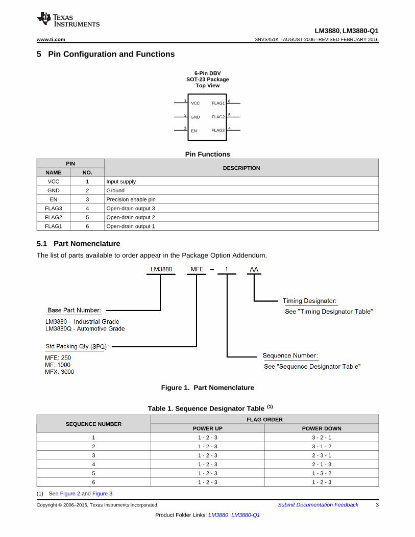
5 Pin Configuration and Functions
6-Pin DBVSOT-23 Package
Top View
Pin FunctionsPIN
DESCRIPTIONNAME NO.VCC 1 Input supplyGND 2 GroundEN 3 Precision enable pin
FLAG3 4 Open-drain output 3FLAG2 5 Open-drain output 2FLAG1 6 Open-drain output 1
(1) See Figure 2 and Figure 3.
5.1 Part NomenclatureThe list of parts available to order appear in the Package Option Addendum.
Figure 1. Part Nomenclature
Table 1. Sequence Designator Table (1)
SEQUENCE NUMBERFLAG ORDER
POWER UP POWER DOWN1 1 - 2 - 3 3 - 2 - 12 1 - 2 - 3 3 - 1 - 23 1 - 2 - 3 2 - 3 - 14 1 - 2 - 3 2 - 1 - 35 1 - 2 - 3 1 - 3 - 26 1 - 2 - 3 1 - 2 - 3

4
LM3880, LM3880-Q1SNVS451K –AUGUST 2006–REVISED FEBRUARY 2016 www.ti.com
Product Folder Links: LM3880 LM3880-Q1
Submit Documentation Feedback Copyright © 2006–2016, Texas Instruments Incorporated
(1) See Figure 2 and Figure 3.
Table 2. Timing Designator Table (1)
TIMINGDESIGNATOR td1 td2 td3 td4 td5 td6
AA 10 ms 10 ms 10 ms 10 ms 10 ms 10 msAB 30 ms 30 ms 30 ms 30 ms 30 ms 30 msAC 60 ms 60 ms 60 ms 60 ms 60 ms 60 msAD 120 ms 120 ms 120 ms 120 ms 120 ms 120 msAE 2 ms 2 ms 2 ms 2 ms 2 ms 2 msAF 16 ms 16 ms 16 ms 16 ms 16 ms 16 ms

5
LM3880, LM3880-Q1www.ti.com SNVS451K –AUGUST 2006–REVISED FEBRUARY 2016
Product Folder Links: LM3880 LM3880-Q1
Submit Documentation FeedbackCopyright © 2006–2016, Texas Instruments Incorporated
(1) Stresses beyond those listed under Absolute Maximum Ratings may cause permanent damage to the device. These are stress ratingsonly, which do not imply functional operation of the device at these or any other conditions beyond those indicated under RecommendedOperating Conditions. Exposure to absolute-maximum-rated conditions for extended periods may affect device reliability.
(2) If Military/Aerospace specified devices are required, please contact the Texas Instruments Sales Office/Distributors for availability andspecifications.
6 Specifications
6.1 Absolute Maximum Ratingsover operating free-air temperature (unless otherwise noted) (1) (2)
MIN MAX UNITVCC −0.3 6.0 VEN, FLAG1, FLAG2, FLAG3 −0.3 6.0 VMax Flag ON Current 50 mAMax Junction Temperature 150 °CLead Temperature (Soldering, 5 s) 260 °CStorage temperature Tstg –65 150 °C
(1) JEDEC document JEP155 states that 500-V HBM allows safe manufacturing with a standard ESD control process.
6.2 ESD Ratings LM3880VALUE UNIT
V(ESD) Electrostatic discharge Human body model (HBM), per ANSI/ESDA/JEDEC JS-001, all pins (1) ±2 kV
(1) AEC Q100-002 indicates HBM stressing is done in accordance with the ANSI/ESDA/JEDEC JS-001 specification.
6.3 ESD Ratings LM3880-Q1MAX UNIT
V(ESD) Electrostatic discharge Human body model (HBM), per AEC Q100-002 (1) ±2 kV
6.4 Recommended Operating Conditionsover operating free-air temperature range (unless otherwise noted)
MIN NOM MAX UNITVCC to GND 2.7 5.5 VEN, FLAG1, FLAG2, FLAG3 −0.3 VCC + 0.3 VJunction Temperature −40 125 °C
(1) For more information about traditional and new thermal metrics, see the IC Package Thermal Metrics application report, SPRA953.
6.5 Thermal Information
THERMAL METRIC (1)
LM3880/LM3880-Q1
UNITDBV6 PINS
RθJA Junction-to-ambient thermal resistance 187.6
°C/WRθJC(top) Junction-to-case (top) thermal resistance 127.4RθJB Junction-to-board thermal resistance 31.5ψJT Junction-to-top characterization parameter 23.3ψJB Junction-to-board characterization parameter 31.0

EN
FLAG1
FLAG2
FLAG3
td1 td2 td3
6
LM3880, LM3880-Q1SNVS451K –AUGUST 2006–REVISED FEBRUARY 2016 www.ti.com
Product Folder Links: LM3880 LM3880-Q1
Submit Documentation Feedback Copyright © 2006–2016, Texas Instruments Incorporated
(1) Limits are 100% production tested at 25°. Limits over the operating temperature range are ensured through correlation using StatisticalQuality Control (SQC) methods. The limits are used to calculate TI's Average Outgoing Quality Level (AOQL).
(2) Typical numbers are at 25°C and represent the most likely parametric norm.
6.6 Electrical CharacteristicsLimits apply to all timing options and VCC = 3.3V, unless otherwise specified. Minimum and Maximum limits apply over the fullOperating Temperature Range (TJ = -40°C to +125°C) and are specified through test, design or statistical correlation. Typicalvalues represent the most likely parametric norm at TJ = 25°C and are provided for reference purposes only.
PARAMETER TEST CONDITIONS MIN (1) TYP (2) MAX (1) UNITIQ Operating Quiescent current 25 80 µAOPEN-DRAIN FLAGSIFLAG FLAGx Leakage Current VFLAGx = 3.3 V 1 20 nAVOL FLAGx Output Voltage Low IFLAGx = 1.2 mA 0.4 VPOWER-UP SEQUENCEtd1 Timer delay 1 accuracy All Other Timing Options –15% 15%
2 ms Timing Option –20% 20%td2 Timer delay 2 accuracy All Other Timing Options –15% 15%
2 ms Timing Option –20% 20%td3 Timer delay 3 accuracy All Other Timing Options –15% 15%
2 ms Timing Option –20% 20%POWER-DOWN SEQUENCEtd4 Timer delay 4 accuracy All Other Timing Options –15% 15%
2 ms Timing Option –20% 20%td5 Timer delay 5 accuracy All Other Timing Options –15% 15%
2 ms Timing Option –20% 20%td6 Timer delay 6 accuracy All Other Timing Options –15% 15%
2 ms Timing Option –20% 20%TIMING DELAY ERROR(td(x) – 400µs) / td(x+1)
Ratio of timing delays For x = 1 or 4 95% 105%For x = 1 or 4, 2 ms option 90% 110%
td(x) / td(x+1) Ratio of timing delays For x = 2 or 5 95% 105%For x = 2 or 5, 2 ms option 90% 110%
ENABLE PINVEN EN pin threshold 1.0 1.25 1.4 VIEN EN pin pullup current VEN = 0 V 7 µA
Timing Requirements
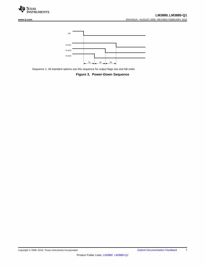
Sequence 1: All standard options use this sequence for output flags rise and fall order.
Figure 2. Power-Up Sequence
EN
FLAG1
FLAG2
FLAG3
td4 td5 td6
7
LM3880, LM3880-Q1www.ti.com SNVS451K –AUGUST 2006–REVISED FEBRUARY 2016
Product Folder Links: LM3880 LM3880-Q1
Submit Documentation FeedbackCopyright © 2006–2016, Texas Instruments Incorporated
Sequence 1: All standard options use this sequence for output flags rise and fall order.
Figure 3. Power-Down Sequence

-40 125
VE
N (
V)
TEMPERATURE (°C)
1.216
1.220
1.222
1.224
1.226
1.228
1.230
1.218
5 35 65 95-10 20 50 80 110-251.214
1.232
RISING
FALLING
2.5 3 3.5 4 4.5 5 5.520
21
22
23
24
25
26
27
28
29
30I Q
(P
A)
VCC (V)
-40 125
I Q (P
A)
TEMPERATURE (oC)
5 35 65 95-10 20 50 80 110-2520
26
21
23
24
25
22
8
LM3880, LM3880-Q1SNVS451K –AUGUST 2006–REVISED FEBRUARY 2016 www.ti.com
Product Folder Links: LM3880 LM3880-Q1
Submit Documentation Feedback Copyright © 2006–2016, Texas Instruments Incorporated
6.7 Typical Characteristics
Figure 4. Quiescent Current vs VCC Figure 5. Quiescent Current vs Temperature (VCC = 3.3 V)
Figure 6. Enable Threshold vs Temperature Figure 7. Time Delay (30 ms) vs Vcc
Figure 8. Time Delay Ratio vs Temperature Figure 9. Time Delay (30 ms) vs Temperature

9
LM3880, LM3880-Q1www.ti.com SNVS451K –AUGUST 2006–REVISED FEBRUARY 2016
Product Folder Links: LM3880 LM3880-Q1
Submit Documentation FeedbackCopyright © 2006–2016, Texas Instruments Incorporated
Typical Characteristics (continued)
Figure 10. Flag VOL vs Vcc (RFLAG = 100 kΩ) Figure 11. Flag Voltage vs Current

GND
VCC
FLAG1
FLAG2
FLAG3
SequenceControl
EN
TimingDelay
Generation
MasterClock
EPROM(Factory Set)
+
-
1.25V
td1
td2
td3
td4
td5
td6
7 PA
10
LM3880, LM3880-Q1SNVS451K –AUGUST 2006–REVISED FEBRUARY 2016 www.ti.com
Product Folder Links: LM3880 LM3880-Q1
Submit Documentation Feedback Copyright © 2006–2016, Texas Instruments Incorporated
7 Detailed Description
7.1 OverviewThe LM3880 Simple Power Supply Sequencer provides a simple solution for sequencing multiple rails in acontrolled manner. Six independent timers are integrated to control the timing sequence (power up and powerdown) of three open-drain output flags. These flags permit connection to either a shutdown or enable pin of linearregulators and switchers to control the operation of the power supplies. This allows design of a complete powersystem without concern for large inrush currents or latch-up conditions that can occur.
The timing sequence of the LM3880 is controlled entirely by the enable (EN) pin. Upon power up, all the flagsare held low until this precision enable is pulled high. When the EN pin is asserted, the power-up sequencestarts. An internal counter delays the first flag (FLAG1) from rising until a fixed time period has expired. When thefirst flag is released, another timer will begin to delay the release of the second flag (FLAG2). This processrepeats until all three flags have sequentially been released.
The power-down sequence is the same as power-up sequence, but in reverse. When the EN pin is deasserted atimer will begin that delays the third flag (FLAG3) from pulling low. The second and first flag will then follow in asequential manner after their appropriate delays. The three timers that are used to control the power-downscheme can also be individually programmed and are completely independent of the power-up timers.
7.2 Functional Block Diagram
7.3 Feature Description
7.3.1 Enable Pin OperationThe timing sequence of the LM3880 is controlled by the assertion of the enable signal. The enable pin isdesigned with an internal comparator, referenced to a bandgap voltage (1.25 V), to provide a precision threshold.This allows a delayed timing to be externally set using a capacitor or to start the sequencing based on a certainevent, such as a line voltage reaching 90% of nominal. For an additional delayed sequence from the railpowering VCC, simply attach a capacitor to the EN pin as shown in Figure 12.

EN
FLAG1
td1
tenable_delay =1.25V x CEN
7 PA
1.25V -
+
7 PA
Enable
CEN
EN
11
LM3880, LM3880-Q1www.ti.com SNVS451K –AUGUST 2006–REVISED FEBRUARY 2016
Product Folder Links: LM3880 LM3880-Q1
Submit Documentation FeedbackCopyright © 2006–2016, Texas Instruments Incorporated
Feature Description (continued)
Figure 12. Capacitor Timing
Using the internal pullup current source to charge the external capacitor (CEN) the enable pin delay can becalculated by Equation 1:
(1)
A resistor divider can also be used to enable the LM3880 based on a certain voltage threshold. Take care whensizing the resistor divider to include the effects of the internal current source.
One of the features of the EN pin is that it provides glitch free operation. The first timer will start counting at arising threshold, but will always reset if the EN pin is deasserted before the first output flag is released. This canbe shown in Figure 13:
Figure 13. EN Glitch
7.3.2 Incomplete Sequence OperationIf the enable signal remains high for the entire power-up sequence, then the part will operate as shown in thestandard timing diagrams. However, if the enable signal is de-asserted before the power-up sequence iscompleted the part will enter a controlled shutdown. This allows the system to walk through a controlled powercycling, preventing any latch conditions from occurring. This state only occurs if the enable pin is deassertedafter the completion of timer 1, but before the entire power-up sequence is completed.
When this event occurs, the falling edge of EN pin resets the current timer and will allow the remaining power-upcycle to complete before beginning the power-down sequence. The power down sequence starts approximately120 ms after the final power-up flag. This allows output voltages in the system to stabilize before everything isshut down. An example of this operation can be seen in Figure 14:

FLAG1
FLAG2
FLAG3
EN
ttd1t ttd2t ttd3t t120 mst ttd4t ttd5t ttd6t
EN
FLAG1
FLAG2
FLAG3
td2td1 td3 120 ms td4 td5 td6
12
LM3880, LM3880-Q1SNVS451K –AUGUST 2006–REVISED FEBRUARY 2016 www.ti.com
Product Folder Links: LM3880 LM3880-Q1
Submit Documentation Feedback Copyright © 2006–2016, Texas Instruments Incorporated
Feature Description (continued)
Figure 14. Incomplete Power-Up Sequence
When the enable signal is deasserted, the part will commence its power-down sequence. If the enable signal ispulled high before the power-down sequence is completed, the part will ensure completion of the power-downsequence before starting power-up. This ensures that the system does not partially power down and power upand helps prevent latch-up events, such as in FPGAs and microprocessors. This state only occurs if the enablepin is pulled high after the completion of timer 1, but before the entire power-down sequence is completed.
When this event occurs, the rising edge of enable pin resets the current timer and will allow the remaining power-down cycle to complete before beginning the power-up sequence. The power-up sequence starts approximately120 ms after the final power-down flag. This allows the system to fully shut down before it is powered up. Anexample of this operation can be seen in Figure 15:
Figure 15. Incomplete Power-Down Sequence
All the internal timers are generated by a master clock that has an extremely low tempco. This allows for tightaccuracy across temperature and a consistent ratio between the individual timers. There is a slight additionaldelay of approximately 400 µs to timers 1 and 4, which is a result of the EPROM refresh. This refresh time is inaddition to the programmed delay time and will be almost insignificant to all but the shortest of timer delays.
13
LM3880, LM3880-Q1www.ti.com SNVS451K –AUGUST 2006–REVISED FEBRUARY 2016
Product Folder Links: LM3880 LM3880-Q1
Submit Documentation FeedbackCopyright © 2006–2016, Texas Instruments Incorporated
7.4 Device Functional Modes
7.4.1 Power Up With EN PinThe timing sequence of the Simple Power Supply Sequencer is controlled entirely by the enable (EN) pin. Uponpower up, all the flags are held low until this precision enable is pulled high. After the EN pin is asserted, thepower-up sequence will commence.
7.4.2 Power Down With EN PinWhen EN pin is deasserted, the power down sequence will commence. A timer will begin that delays the thirdflag (FLAG3) from pulling low. The second and first flag will then follow in a sequential manner after theirappropriate delays.
14
LM3880, LM3880-Q1SNVS451K –AUGUST 2006–REVISED FEBRUARY 2016 www.ti.com
Product Folder Links: LM3880 LM3880-Q1
Submit Documentation Feedback Copyright © 2006–2016, Texas Instruments Incorporated
8 Application and Implementation
NOTEInformation in the following applications sections is not part of the TI componentspecification, and TI does not warrant its accuracy or completeness. TI’s customers areresponsible for determining suitability of components for their purposes. Customers shouldvalidate and test their design implementation to confirm system functionality.
8.1 Application Information
8.1.1 Open Drain Flags PullupThe Simple Power Supply Sequencer contains three open-drain output flags which need to be pulled up forproper operation. 100-kΩ resistors can be used as pullup resistors.
8.1.2 Enable the DeviceSee Enable Pin Operation.
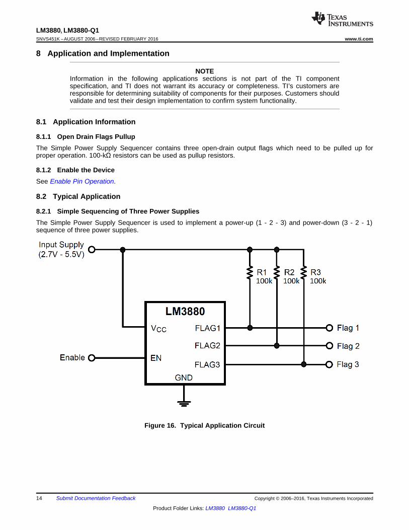
8.2 Typical Application
8.2.1 Simple Sequencing of Three Power SuppliesThe Simple Power Supply Sequencer is used to implement a power-up (1 - 2 - 3) and power-down (3 - 2 - 1)sequence of three power supplies.
Figure 16. Typical Application Circuit
15
LM3880, LM3880-Q1www.ti.com SNVS451K –AUGUST 2006–REVISED FEBRUARY 2016
Product Folder Links: LM3880 LM3880-Q1
Submit Documentation FeedbackCopyright © 2006–2016, Texas Instruments Incorporated
Typical Application (continued)8.2.1.1 Design RequirementsFor this design example, use the parameters listed in Table 3 as the input parameters.
Table 3. Design ParametersDesign Parameter Example Value
Input Supply voltage range 2.7 V to 5.5 VFlag Output voltage, EN high Input SupplyFlag Output voltage, EN low 0 V
Flag Timing Delay 30 msPower-Up Sequence 1 - 2 - 3
Power-Down Sequence 3 - 2 - 1
8.2.1.2 Detailed Design Procedure
Table 4. Bill of MaterialsDesignator Description Part # Quantity Manufacturer
U1 LM3880, Sequence 1, 30 ms timing LM3880 1 Texas InstrumentsR1 100K Resistor, 0603 CRCW0603100KFKEA 1 VishayR2 100K Resistor, 0603 CRCW0603100KFKEA 1 VishayR3 100K Resistor, 0603 CRCW0603100KFKEA 1 Vishay
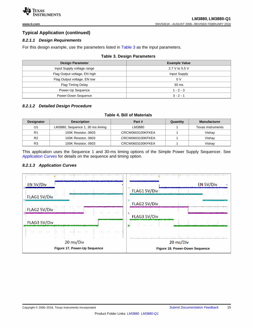
This application uses the Sequence 1 and 30-ms timing options of the Simple Power Supply Sequencer. SeeApplication Curves for details on the sequence and timing option.
8.2.1.3 Application Curves
Figure 17. Power-Up Sequence Figure 18. Power-Down Sequence
16
LM3880, LM3880-Q1SNVS451K –AUGUST 2006–REVISED FEBRUARY 2016 www.ti.com
Product Folder Links: LM3880 LM3880-Q1
Submit Documentation Feedback Copyright © 2006–2016, Texas Instruments Incorporated
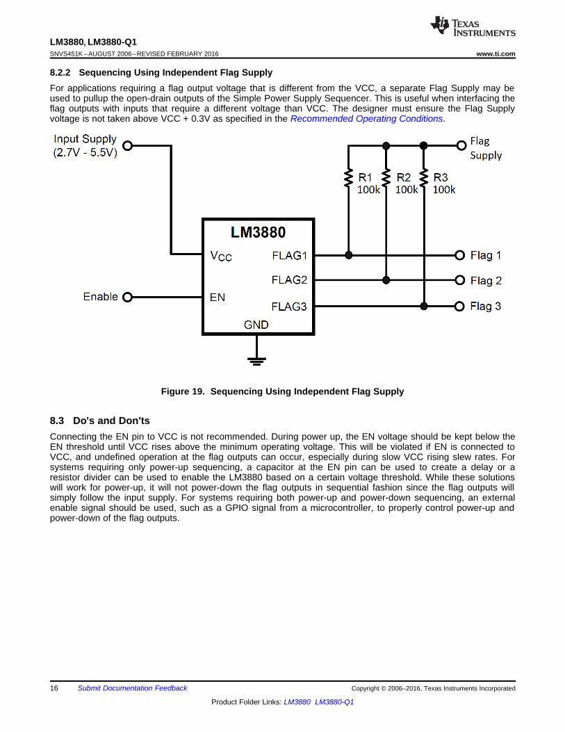
8.2.2 Sequencing Using Independent Flag SupplyFor applications requiring a flag output voltage that is different from the VCC, a separate Flag Supply may beused to pullup the open-drain outputs of the Simple Power Supply Sequencer. This is useful when interfacing theflag outputs with inputs that require a different voltage than VCC. The designer must ensure the Flag Supplyvoltage is not taken above VCC + 0.3V as specified in the Recommended Operating Conditions.
Figure 19. Sequencing Using Independent Flag Supply
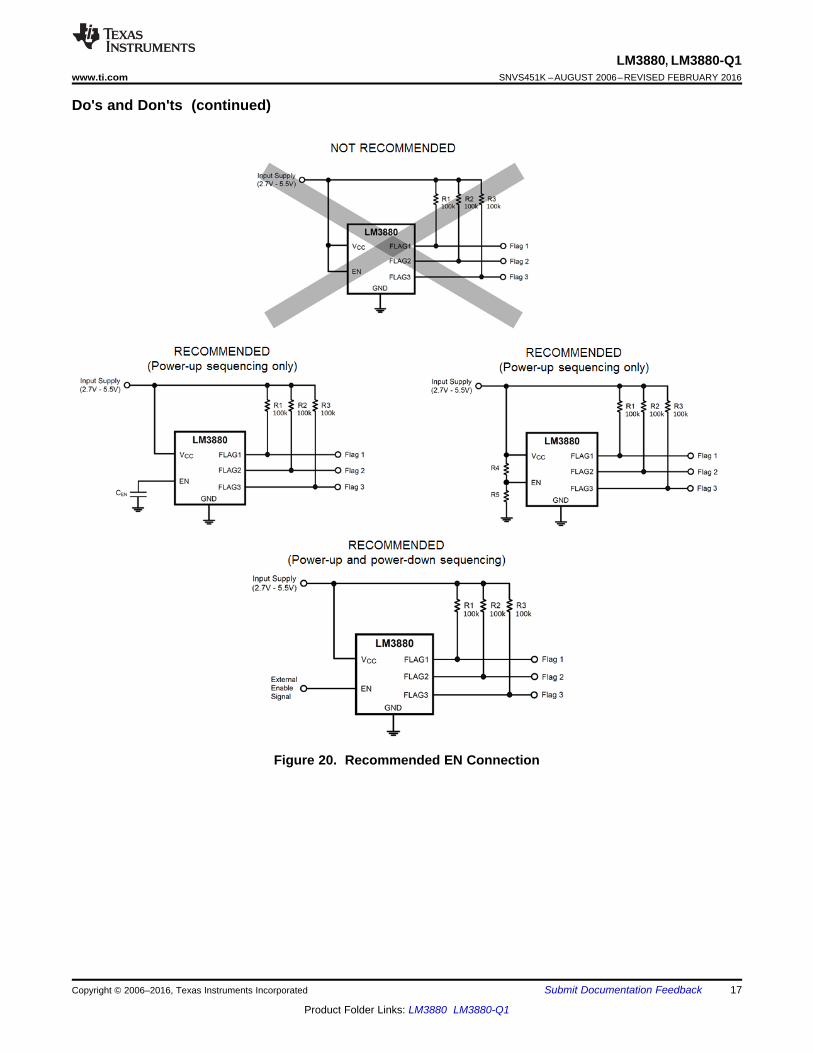
8.3 Do's and Don'tsConnecting the EN pin to VCC is not recommended. During power up, the EN voltage should be kept below theEN threshold until VCC rises above the minimum operating voltage. This will be violated if EN is connected toVCC, and undefined operation at the flag outputs can occur, especially during slow VCC rising slew rates. Forsystems requiring only power-up sequencing, a capacitor at the EN pin can be used to create a delay or aresistor divider can be used to enable the LM3880 based on a certain voltage threshold. While these solutionswill work for power-up, it will not power-down the flag outputs in sequential fashion since the flag outputs willsimply follow the input supply. For systems requiring both power-up and power-down sequencing, an externalenable signal should be used, such as a GPIO signal from a microcontroller, to properly control power-up andpower-down of the flag outputs.
17
LM3880, LM3880-Q1www.ti.com SNVS451K –AUGUST 2006–REVISED FEBRUARY 2016
Product Folder Links: LM3880 LM3880-Q1
Submit Documentation FeedbackCopyright © 2006–2016, Texas Instruments Incorporated
Do's and Don'ts (continued)
Figure 20. Recommended EN Connection
18
LM3880, LM3880-Q1SNVS451K –AUGUST 2006–REVISED FEBRUARY 2016 www.ti.com
Product Folder Links: LM3880 LM3880-Q1
Submit Documentation Feedback Copyright © 2006–2016, Texas Instruments Incorporated
9 Power Supply RecommendationsThe VCC pin should be located as close as possible to the input supply (2.7V - 5.5V). An input capacitor is notrequired but is recommended when noise might be present on the VCC pin. A 0.1 μF ceramic capacitor may beused to bypass this noise.
10 Layout
10.1 Layout Guidelines• Pullup resistors should be connected between the flag output pins and a positive input supply, usually VCC.
An independent flag supply may also be used. These resistors should be placed as close as possible to theSimple Power Supply Sequencer and the flag supply. Minimal trace length is recommended to make theconnections. A typical value for the pullup resistors is 100kΩ.
• For very tight sequencing requirements, minimal and equal trace lengths should be used to connect the flagoutputs to the desired inputs. This will reduce any propagation delay and timing errors between the flagoutputs along the line.
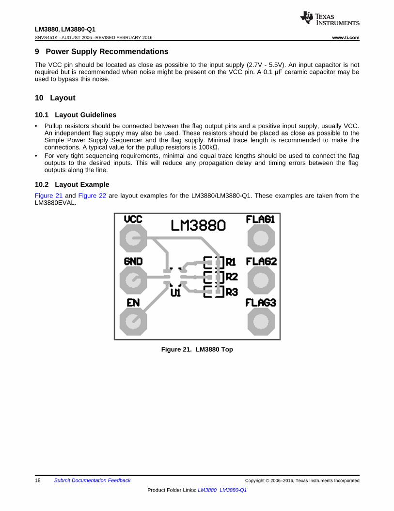
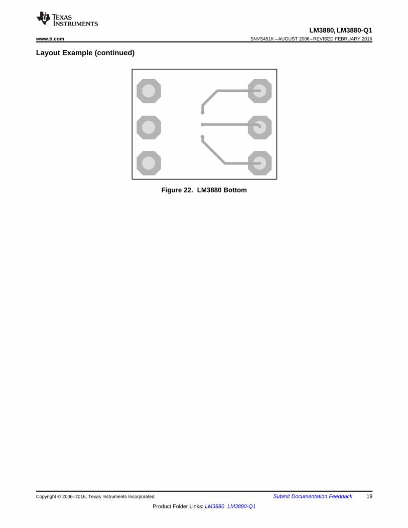
10.2 Layout ExampleFigure 21 and Figure 22 are layout examples for the LM3880/LM3880-Q1. These examples are taken from theLM3880EVAL.
Figure 21. LM3880 Top
19
LM3880, LM3880-Q1www.ti.com SNVS451K –AUGUST 2006–REVISED FEBRUARY 2016
Product Folder Links: LM3880 LM3880-Q1
Submit Documentation FeedbackCopyright © 2006–2016, Texas Instruments Incorporated
Layout Example (continued)
Figure 22. LM3880 Bottom
20
LM3880, LM3880-Q1SNVS451K –AUGUST 2006–REVISED FEBRUARY 2016 www.ti.com
Product Folder Links: LM3880 LM3880-Q1
Submit Documentation Feedback Copyright © 2006–2016, Texas Instruments Incorporated
11 Device and Documentation Support
11.1 Device Support
11.1.1 Third-Party Products DisclaimerTI'S PUBLICATION OF INFORMATION REGARDING THIRD-PARTY PRODUCTS OR SERVICES DOES NOTCONSTITUTE AN ENDORSEMENT REGARDING THE SUITABILITY OF SUCH PRODUCTS OR SERVICESOR A WARRANTY, REPRESENTATION OR ENDORSEMENT OF SUCH PRODUCTS OR SERVICES, EITHERALONE OR IN COMBINATION WITH ANY TI PRODUCT OR SERVICE.
11.2 Community ResourcesThe following links connect to TI community resources. Linked contents are provided "AS IS" by the respectivecontributors. They do not constitute TI specifications and do not necessarily reflect TI's views; see TI's Terms ofUse.
TI E2E™ Online Community TI's Engineer-to-Engineer (E2E) Community. Created to foster collaborationamong engineers. At e2e.ti.com, you can ask questions, share knowledge, explore ideas and helpsolve problems with fellow engineers.
Design Support TI's Design Support Quickly find helpful E2E forums along with design support tools andcontact information for technical support.
11.3 Related LinksThe table below lists quick access links. Categories include technical documents, support and communityresources, tools and software, and quick access to sample or buy.
Table 5. Related Links
PARTS PRODUCT FOLDER SAMPLE & BUY TECHNICALDOCUMENTS
TOOLS &SOFTWARE
SUPPORT &COMMUNITY
LM3880 Click here Click here Click here Click here Click hereLM3880-Q1 Click here Click here Click here Click here Click here
11.4 TrademarksE2E is a trademark of Texas Instruments.All other trademarks are the property of their respective owners.
11.5 Electrostatic Discharge CautionThese devices have limited built-in ESD protection. The leads should be shorted together or the device placed in conductive foamduring storage or handling to prevent electrostatic damage to the MOS gates.
11.6 GlossarySLYZ022 — TI Glossary.
This glossary lists and explains terms, acronyms, and definitions.
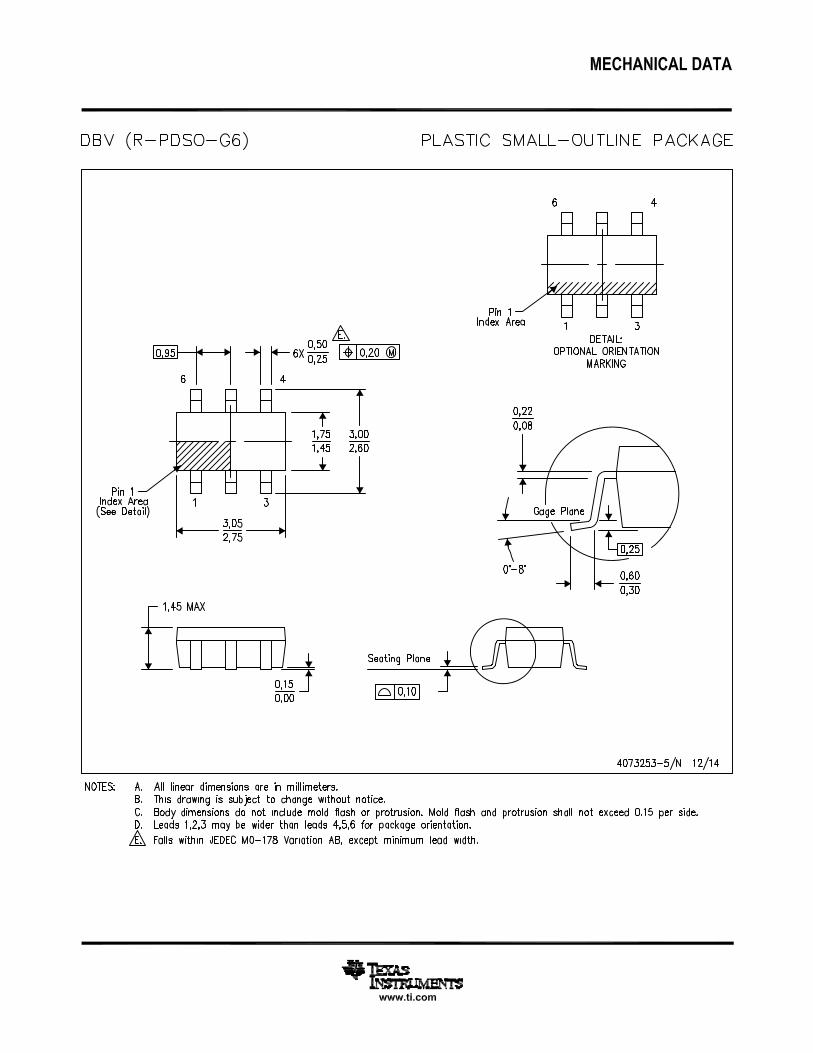
12 Mechanical, Packaging, and Orderable InformationThe following pages include mechanical, packaging, and orderable information. This information is the mostcurrent data available for the designated devices. This data is subject to change without notice and revision ofthis document. For browser-based versions of this data sheet, refer to the left-hand navigation.
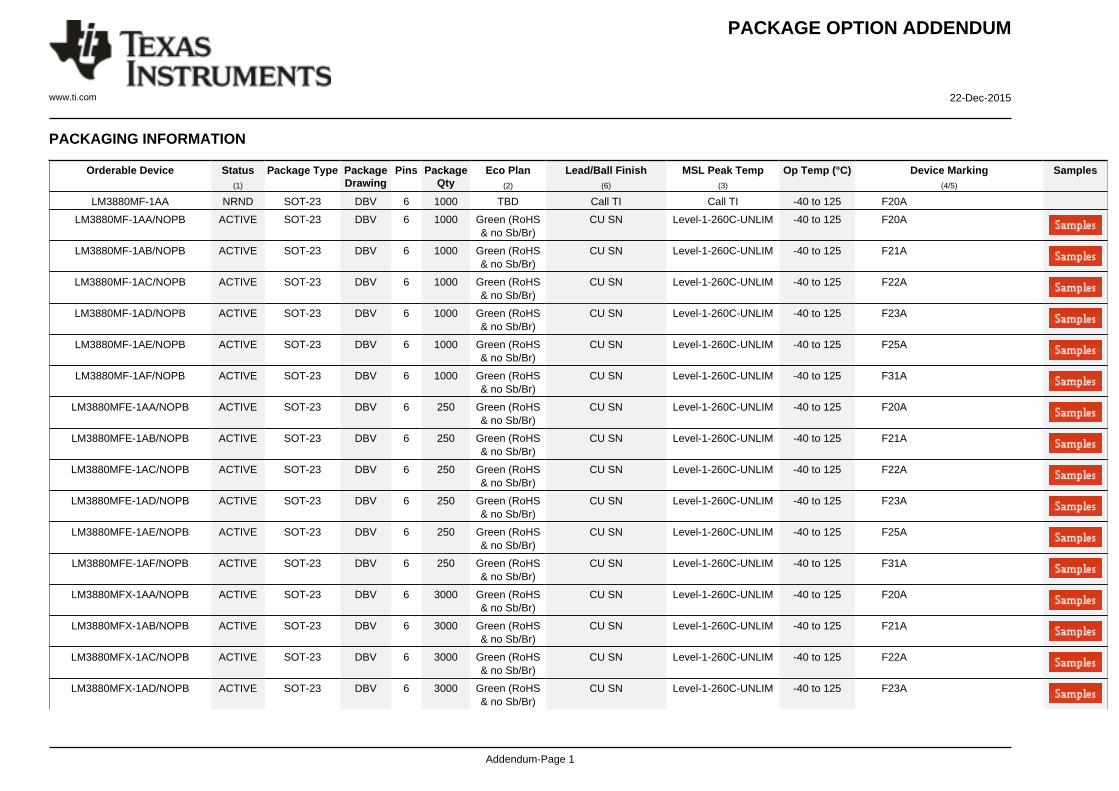
PACKAGE OPTION ADDENDUM
www.ti.com 22-Dec-2015
Addendum-Page 1
PACKAGING INFORMATION
Orderable Device Status(1)
Package Type PackageDrawing
Pins PackageQty
Eco Plan(2)
Lead/Ball Finish(6)
MSL Peak Temp(3)
Op Temp (°C) Device Marking(4/5)
Samples
LM3880MF-1AA NRND SOT-23 DBV 6 1000 TBD Call TI Call TI -40 to 125 F20A
LM3880MF-1AA/NOPB ACTIVE SOT-23 DBV 6 1000 Green (RoHS& no Sb/Br)
CU SN Level-1-260C-UNLIM -40 to 125 F20A
LM3880MF-1AB/NOPB ACTIVE SOT-23 DBV 6 1000 Green (RoHS& no Sb/Br)
CU SN Level-1-260C-UNLIM -40 to 125 F21A
LM3880MF-1AC/NOPB ACTIVE SOT-23 DBV 6 1000 Green (RoHS& no Sb/Br)
CU SN Level-1-260C-UNLIM -40 to 125 F22A
LM3880MF-1AD/NOPB ACTIVE SOT-23 DBV 6 1000 Green (RoHS& no Sb/Br)
CU SN Level-1-260C-UNLIM -40 to 125 F23A
LM3880MF-1AE/NOPB ACTIVE SOT-23 DBV 6 1000 Green (RoHS& no Sb/Br)
CU SN Level-1-260C-UNLIM -40 to 125 F25A
LM3880MF-1AF/NOPB ACTIVE SOT-23 DBV 6 1000 Green (RoHS& no Sb/Br)
CU SN Level-1-260C-UNLIM -40 to 125 F31A
LM3880MFE-1AA/NOPB ACTIVE SOT-23 DBV 6 250 Green (RoHS& no Sb/Br)
CU SN Level-1-260C-UNLIM -40 to 125 F20A
LM3880MFE-1AB/NOPB ACTIVE SOT-23 DBV 6 250 Green (RoHS& no Sb/Br)
CU SN Level-1-260C-UNLIM -40 to 125 F21A
LM3880MFE-1AC/NOPB ACTIVE SOT-23 DBV 6 250 Green (RoHS& no Sb/Br)
CU SN Level-1-260C-UNLIM -40 to 125 F22A
LM3880MFE-1AD/NOPB ACTIVE SOT-23 DBV 6 250 Green (RoHS& no Sb/Br)
CU SN Level-1-260C-UNLIM -40 to 125 F23A
LM3880MFE-1AE/NOPB ACTIVE SOT-23 DBV 6 250 Green (RoHS& no Sb/Br)
CU SN Level-1-260C-UNLIM -40 to 125 F25A
LM3880MFE-1AF/NOPB ACTIVE SOT-23 DBV 6 250 Green (RoHS& no Sb/Br)
CU SN Level-1-260C-UNLIM -40 to 125 F31A
LM3880MFX-1AA/NOPB ACTIVE SOT-23 DBV 6 3000 Green (RoHS& no Sb/Br)
CU SN Level-1-260C-UNLIM -40 to 125 F20A
LM3880MFX-1AB/NOPB ACTIVE SOT-23 DBV 6 3000 Green (RoHS& no Sb/Br)
CU SN Level-1-260C-UNLIM -40 to 125 F21A
LM3880MFX-1AC/NOPB ACTIVE SOT-23 DBV 6 3000 Green (RoHS& no Sb/Br)
CU SN Level-1-260C-UNLIM -40 to 125 F22A
LM3880MFX-1AD/NOPB ACTIVE SOT-23 DBV 6 3000 Green (RoHS& no Sb/Br)
CU SN Level-1-260C-UNLIM -40 to 125 F23A

PACKAGE OPTION ADDENDUM
www.ti.com 22-Dec-2015
Addendum-Page 2
Orderable Device Status(1)
Package Type PackageDrawing
Pins PackageQty
Eco Plan(2)
Lead/Ball Finish(6)
MSL Peak Temp(3)
Op Temp (°C) Device Marking(4/5)
Samples
LM3880MFX-1AE/NOPB ACTIVE SOT-23 DBV 6 3000 Green (RoHS& no Sb/Br)
CU SN Level-1-260C-UNLIM -40 to 125 F25A
LM3880MFX-1AF/NOPB ACTIVE SOT-23 DBV 6 3000 Green (RoHS& no Sb/Br)
CU SN Level-1-260C-UNLIM -40 to 125 F31A
LM3880QMF-1AA/NOPB ACTIVE SOT-23 DBV 6 1000 Green (RoHS& no Sb/Br)
CU SN Level-1-260C-UNLIM -40 to 125 F27A
LM3880QMF-1AB/NOPB ACTIVE SOT-23 DBV 6 1000 Green (RoHS& no Sb/Br)
CU SN Level-1-260C-UNLIM -40 to 125 F28A
LM3880QMF-1AC/NOPB ACTIVE SOT-23 DBV 6 1000 Green (RoHS& no Sb/Br)
CU SN Level-1-260C-UNLIM -40 to 125 F29A
LM3880QMF-1AD/NOPB ACTIVE SOT-23 DBV 6 1000 Green (RoHS& no Sb/Br)
CU SN Level-1-260C-UNLIM -40 to 125 F30A
LM3880QMF-1AE/NOPB ACTIVE SOT-23 DBV 6 1000 Green (RoHS& no Sb/Br)
CU SN Level-1-260C-UNLIM -40 to 125 F24A
LM3880QMF-1AF/NOPB ACTIVE SOT-23 DBV 6 1000 Green (RoHS& no Sb/Br)
CU SN Level-1-260C-UNLIM -40 to 125 F32A
LM3880QMFE-1AA/NOPB ACTIVE SOT-23 DBV 6 250 Green (RoHS& no Sb/Br)
CU SN Level-1-260C-UNLIM -40 to 125 F27A
LM3880QMFE-1AB/NOPB ACTIVE SOT-23 DBV 6 250 Green (RoHS& no Sb/Br)
CU SN Level-1-260C-UNLIM -40 to 125 F28A
LM3880QMFE-1AC/NOPB ACTIVE SOT-23 DBV 6 250 Green (RoHS& no Sb/Br)
CU SN Level-1-260C-UNLIM -40 to 125 F29A
LM3880QMFE-1AD/NOPB ACTIVE SOT-23 DBV 6 250 Green (RoHS& no Sb/Br)
CU SN Level-1-260C-UNLIM -40 to 125 F30A
LM3880QMFE-1AE/NOPB ACTIVE SOT-23 DBV 6 250 Green (RoHS& no Sb/Br)
CU SN Level-1-260C-UNLIM -40 to 125 F24A
LM3880QMFE-1AF/NOPB ACTIVE SOT-23 DBV 6 250 Green (RoHS& no Sb/Br)
CU SN Level-1-260C-UNLIM -40 to 125 F32A
LM3880QMFX-1AA/NOPB ACTIVE SOT-23 DBV 6 3000 Green (RoHS& no Sb/Br)
CU SN Level-1-260C-UNLIM -40 to 125 F27A
LM3880QMFX-1AB/NOPB ACTIVE SOT-23 DBV 6 3000 Green (RoHS& no Sb/Br)
CU SN Level-1-260C-UNLIM -40 to 125 F28A
LM3880QMFX-1AC/NOPB ACTIVE SOT-23 DBV 6 3000 Green (RoHS& no Sb/Br)
CU SN Level-1-260C-UNLIM -40 to 125 F29A
LM3880QMFX-1AD/NOPB ACTIVE SOT-23 DBV 6 3000 Green (RoHS& no Sb/Br)
CU SN Level-1-260C-UNLIM -40 to 125 F30A
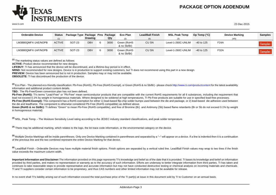
PACKAGE OPTION ADDENDUM
www.ti.com 22-Dec-2015
Addendum-Page 3
Orderable Device Status(1)
Package Type PackageDrawing
Pins PackageQty
Eco Plan(2)
Lead/Ball Finish(6)
MSL Peak Temp(3)
Op Temp (°C) Device Marking(4/5)
Samples
LM3880QMFX-1AE/NOPB ACTIVE SOT-23 DBV 6 3000 Green (RoHS& no Sb/Br)
CU SN Level-1-260C-UNLIM -40 to 125 F24A
LM3880QMFX-1AF/NOPB ACTIVE SOT-23 DBV 6 3000 Green (RoHS& no Sb/Br)
CU SN Level-1-260C-UNLIM -40 to 125 F32A
(1) The marketing status values are defined as follows:ACTIVE: Product device recommended for new designs.LIFEBUY: TI has announced that the device will be discontinued, and a lifetime-buy period is in effect.NRND: Not recommended for new designs. Device is in production to support existing customers, but TI does not recommend using this part in a new design.PREVIEW: Device has been announced but is not in production. Samples may or may not be available.OBSOLETE: TI has discontinued the production of the device.
(2) Eco Plan - The planned eco-friendly classification: Pb-Free (RoHS), Pb-Free (RoHS Exempt), or Green (RoHS & no Sb/Br) - please check http://www.ti.com/productcontent for the latest availabilityinformation and additional product content details.TBD: The Pb-Free/Green conversion plan has not been defined.Pb-Free (RoHS): TI's terms "Lead-Free" or "Pb-Free" mean semiconductor products that are compatible with the current RoHS requirements for all 6 substances, including the requirement thatlead not exceed 0.1% by weight in homogeneous materials. Where designed to be soldered at high temperatures, TI Pb-Free products are suitable for use in specified lead-free processes.Pb-Free (RoHS Exempt): This component has a RoHS exemption for either 1) lead-based flip-chip solder bumps used between the die and package, or 2) lead-based die adhesive used betweenthe die and leadframe. The component is otherwise considered Pb-Free (RoHS compatible) as defined above.Green (RoHS & no Sb/Br): TI defines "Green" to mean Pb-Free (RoHS compatible), and free of Bromine (Br) and Antimony (Sb) based flame retardants (Br or Sb do not exceed 0.1% by weightin homogeneous material)
(3) MSL, Peak Temp. - The Moisture Sensitivity Level rating according to the JEDEC industry standard classifications, and peak solder temperature.
(4) There may be additional marking, which relates to the logo, the lot trace code information, or the environmental category on the device.
(5) Multiple Device Markings will be inside parentheses. Only one Device Marking contained in parentheses and separated by a "~" will appear on a device. If a line is indented then it is a continuationof the previous line and the two combined represent the entire Device Marking for that device.
(6) Lead/Ball Finish - Orderable Devices may have multiple material finish options. Finish options are separated by a vertical ruled line. Lead/Ball Finish values may wrap to two lines if the finishvalue exceeds the maximum column width.
Important Information and Disclaimer:The information provided on this page represents TI's knowledge and belief as of the date that it is provided. TI bases its knowledge and belief on informationprovided by third parties, and makes no representation or warranty as to the accuracy of such information. Efforts are underway to better integrate information from third parties. TI has taken andcontinues to take reasonable steps to provide representative and accurate information but may not have conducted destructive testing or chemical analysis on incoming materials and chemicals.TI and TI suppliers consider certain information to be proprietary, and thus CAS numbers and other limited information may not be available for release.
In no event shall TI's liability arising out of such information exceed the total purchase price of the TI part(s) at issue in this document sold by TI to Customer on an annual basis.

PACKAGE OPTION ADDENDUM
www.ti.com 22-Dec-2015
Addendum-Page 4
OTHER QUALIFIED VERSIONS OF LM3880, LM3880-Q1 :
• Catalog: LM3880
• Automotive: LM3880-Q1
NOTE: Qualified Version Definitions:
• Catalog - TI's standard catalog product
• Automotive - Q100 devices qualified for high-reliability automotive applications targeting zero defects

TAPE AND REEL INFORMATION
*All dimensions are nominal
Device PackageType
PackageDrawing
Pins SPQ ReelDiameter
(mm)
ReelWidth
W1 (mm)
A0(mm)
B0(mm)
K0(mm)
P1(mm)
W(mm)
Pin1Quadrant
LM3880MF-1AA SOT-23 DBV 6 1000 178.0 8.4 3.2 3.2 1.4 4.0 8.0 Q3
LM3880MF-1AA/NOPB SOT-23 DBV 6 1000 178.0 8.4 3.2 3.2 1.4 4.0 8.0 Q3
LM3880MF-1AB/NOPB SOT-23 DBV 6 1000 178.0 8.4 3.2 3.2 1.4 4.0 8.0 Q3
LM3880MF-1AC/NOPB SOT-23 DBV 6 1000 178.0 8.4 3.2 3.2 1.4 4.0 8.0 Q3
LM3880MF-1AD/NOPB SOT-23 DBV 6 1000 178.0 8.4 3.2 3.2 1.4 4.0 8.0 Q3
LM3880MF-1AE/NOPB SOT-23 DBV 6 1000 178.0 8.4 3.2 3.2 1.4 4.0 8.0 Q3
LM3880MF-1AF/NOPB SOT-23 DBV 6 1000 178.0 8.4 3.2 3.2 1.4 4.0 8.0 Q3
LM3880MFE-1AA/NOPB SOT-23 DBV 6 250 178.0 8.4 3.2 3.2 1.4 4.0 8.0 Q3
LM3880MFE-1AB/NOPB SOT-23 DBV 6 250 178.0 8.4 3.2 3.2 1.4 4.0 8.0 Q3
LM3880MFE-1AC/NOPB SOT-23 DBV 6 250 178.0 8.4 3.2 3.2 1.4 4.0 8.0 Q3
LM3880MFE-1AD/NOPB SOT-23 DBV 6 250 178.0 8.4 3.2 3.2 1.4 4.0 8.0 Q3
LM3880MFE-1AE/NOPB SOT-23 DBV 6 250 178.0 8.4 3.2 3.2 1.4 4.0 8.0 Q3
LM3880MFE-1AF/NOPB SOT-23 DBV 6 250 178.0 8.4 3.2 3.2 1.4 4.0 8.0 Q3
LM3880MFX-1AA/NOPB SOT-23 DBV 6 3000 178.0 8.4 3.2 3.2 1.4 4.0 8.0 Q3
LM3880MFX-1AB/NOPB SOT-23 DBV 6 3000 178.0 8.4 3.2 3.2 1.4 4.0 8.0 Q3
LM3880MFX-1AC/NOPB SOT-23 DBV 6 3000 178.0 8.4 3.2 3.2 1.4 4.0 8.0 Q3
LM3880MFX-1AD/NOPB SOT-23 DBV 6 3000 178.0 8.4 3.2 3.2 1.4 4.0 8.0 Q3
LM3880MFX-1AE/NOPB SOT-23 DBV 6 3000 178.0 8.4 3.2 3.2 1.4 4.0 8.0 Q3
PACKAGE MATERIALS INFORMATION
www.ti.com 20-Dec-2016
Pack Materials-Page 1

Device PackageType
PackageDrawing
Pins SPQ ReelDiameter
(mm)
ReelWidth
W1 (mm)
A0(mm)
B0(mm)
K0(mm)
P1(mm)
W(mm)
Pin1Quadrant
LM3880MFX-1AF/NOPB SOT-23 DBV 6 3000 178.0 8.4 3.2 3.2 1.4 4.0 8.0 Q3
LM3880QMF-1AA/NOPB SOT-23 DBV 6 1000 178.0 8.4 3.2 3.2 1.4 4.0 8.0 Q3
LM3880QMF-1AB/NOPB SOT-23 DBV 6 1000 178.0 8.4 3.2 3.2 1.4 4.0 8.0 Q3
LM3880QMF-1AC/NOPB SOT-23 DBV 6 1000 178.0 8.4 3.2 3.2 1.4 4.0 8.0 Q3
LM3880QMF-1AD/NOPB SOT-23 DBV 6 1000 178.0 8.4 3.2 3.2 1.4 4.0 8.0 Q3
LM3880QMF-1AE/NOPB SOT-23 DBV 6 1000 178.0 8.4 3.2 3.2 1.4 4.0 8.0 Q3
LM3880QMF-1AF/NOPB SOT-23 DBV 6 1000 178.0 8.4 3.2 3.2 1.4 4.0 8.0 Q3
LM3880QMFE-1AA/NOPB SOT-23 DBV 6 250 178.0 8.4 3.2 3.2 1.4 4.0 8.0 Q3
LM3880QMFE-1AB/NOPB SOT-23 DBV 6 250 178.0 8.4 3.2 3.2 1.4 4.0 8.0 Q3
LM3880QMFE-1AC/NOPB SOT-23 DBV 6 250 178.0 8.4 3.2 3.2 1.4 4.0 8.0 Q3
LM3880QMFE-1AD/NOPB SOT-23 DBV 6 250 178.0 8.4 3.2 3.2 1.4 4.0 8.0 Q3
LM3880QMFE-1AE/NOPB SOT-23 DBV 6 250 178.0 8.4 3.2 3.2 1.4 4.0 8.0 Q3
LM3880QMFE-1AF/NOPB SOT-23 DBV 6 250 178.0 8.4 3.2 3.2 1.4 4.0 8.0 Q3
LM3880QMFX-1AA/NOPB SOT-23 DBV 6 3000 178.0 8.4 3.2 3.2 1.4 4.0 8.0 Q3
LM3880QMFX-1AB/NOPB SOT-23 DBV 6 3000 178.0 8.4 3.2 3.2 1.4 4.0 8.0 Q3
LM3880QMFX-1AC/NOPB SOT-23 DBV 6 3000 178.0 8.4 3.2 3.2 1.4 4.0 8.0 Q3
LM3880QMFX-1AD/NOPB SOT-23 DBV 6 3000 178.0 8.4 3.2 3.2 1.4 4.0 8.0 Q3
LM3880QMFX-1AE/NOPB SOT-23 DBV 6 3000 178.0 8.4 3.2 3.2 1.4 4.0 8.0 Q3
LM3880QMFX-1AF/NOPB SOT-23 DBV 6 3000 178.0 8.4 3.2 3.2 1.4 4.0 8.0 Q3
PACKAGE MATERIALS INFORMATION
www.ti.com 20-Dec-2016
Pack Materials-Page 2

*All dimensions are nominal
Device Package Type Package Drawing Pins SPQ Length (mm) Width (mm) Height (mm)
LM3880MF-1AA SOT-23 DBV 6 1000 210.0 185.0 35.0
LM3880MF-1AA/NOPB SOT-23 DBV 6 1000 210.0 185.0 35.0
LM3880MF-1AB/NOPB SOT-23 DBV 6 1000 210.0 185.0 35.0
LM3880MF-1AC/NOPB SOT-23 DBV 6 1000 210.0 185.0 35.0
LM3880MF-1AD/NOPB SOT-23 DBV 6 1000 210.0 185.0 35.0
LM3880MF-1AE/NOPB SOT-23 DBV 6 1000 210.0 185.0 35.0
LM3880MF-1AF/NOPB SOT-23 DBV 6 1000 210.0 185.0 35.0
LM3880MFE-1AA/NOPB SOT-23 DBV 6 250 210.0 185.0 35.0
LM3880MFE-1AB/NOPB SOT-23 DBV 6 250 210.0 185.0 35.0
LM3880MFE-1AC/NOPB SOT-23 DBV 6 250 210.0 185.0 35.0
LM3880MFE-1AD/NOPB SOT-23 DBV 6 250 210.0 185.0 35.0
LM3880MFE-1AE/NOPB SOT-23 DBV 6 250 210.0 185.0 35.0
LM3880MFE-1AF/NOPB SOT-23 DBV 6 250 210.0 185.0 35.0
LM3880MFX-1AA/NOPB SOT-23 DBV 6 3000 210.0 185.0 35.0
LM3880MFX-1AB/NOPB SOT-23 DBV 6 3000 210.0 185.0 35.0
LM3880MFX-1AC/NOPB SOT-23 DBV 6 3000 210.0 185.0 35.0
LM3880MFX-1AD/NOPB SOT-23 DBV 6 3000 210.0 185.0 35.0
LM3880MFX-1AE/NOPB SOT-23 DBV 6 3000 210.0 185.0 35.0
LM3880MFX-1AF/NOPB SOT-23 DBV 6 3000 210.0 185.0 35.0
LM3880QMF-1AA/NOPB SOT-23 DBV 6 1000 210.0 185.0 35.0
LM3880QMF-1AB/NOPB SOT-23 DBV 6 1000 210.0 185.0 35.0
LM3880QMF-1AC/NOPB SOT-23 DBV 6 1000 210.0 185.0 35.0
LM3880QMF-1AD/NOPB SOT-23 DBV 6 1000 210.0 185.0 35.0
LM3880QMF-1AE/NOPB SOT-23 DBV 6 1000 210.0 185.0 35.0
LM3880QMF-1AF/NOPB SOT-23 DBV 6 1000 210.0 185.0 35.0
LM3880QMFE-1AA/NOPB SOT-23 DBV 6 250 210.0 185.0 35.0
LM3880QMFE-1AB/NOPB SOT-23 DBV 6 250 210.0 185.0 35.0
LM3880QMFE-1AC/NOPB SOT-23 DBV 6 250 210.0 185.0 35.0
LM3880QMFE-1AD/NOPB SOT-23 DBV 6 250 210.0 185.0 35.0
LM3880QMFE-1AE/NOPB SOT-23 DBV 6 250 210.0 185.0 35.0
LM3880QMFE-1AF/NOPB SOT-23 DBV 6 250 210.0 185.0 35.0
LM3880QMFX-1AA/NOPB SOT-23 DBV 6 3000 210.0 185.0 35.0
LM3880QMFX-1AB/NOPB SOT-23 DBV 6 3000 210.0 185.0 35.0
LM3880QMFX-1AC/NOPB SOT-23 DBV 6 3000 210.0 185.0 35.0
LM3880QMFX-1AD/NOPB SOT-23 DBV 6 3000 210.0 185.0 35.0
LM3880QMFX-1AE/NOPB SOT-23 DBV 6 3000 210.0 185.0 35.0
LM3880QMFX-1AF/NOPB SOT-23 DBV 6 3000 210.0 185.0 35.0
PACKAGE MATERIALS INFORMATION
www.ti.com 20-Dec-2016
Pack Materials-Page 3
IMPORTANT NOTICE
Texas Instruments Incorporated and its subsidiaries (TI) reserve the right to make corrections, enhancements, improvements and otherchanges to its semiconductor products and services per JESD46, latest issue, and to discontinue any product or service per JESD48, latestissue. Buyers should obtain the latest relevant information before placing orders and should verify that such information is current andcomplete. All semiconductor products (also referred to herein as “components”) are sold subject to TI’s terms and conditions of salesupplied at the time of order acknowledgment.TI warrants performance of its components to the specifications applicable at the time of sale, in accordance with the warranty in TI’s termsand conditions of sale of semiconductor products. Testing and other quality control techniques are used to the extent TI deems necessaryto support this warranty. Except where mandated by applicable law, testing of all parameters of each component is not necessarilyperformed.TI assumes no liability for applications assistance or the design of Buyers’ products. Buyers are responsible for their products andapplications using TI components. To minimize the risks associated with Buyers’ products and applications, Buyers should provideadequate design and operating safeguards.TI does not warrant or represent that any license, either express or implied, is granted under any patent right, copyright, mask work right, orother intellectual property right relating to any combination, machine, or process in which TI components or services are used. Informationpublished by TI regarding third-party products or services does not constitute a license to use such products or services or a warranty orendorsement thereof. Use of such information may require a license from a third party under the patents or other intellectual property of thethird party, or a license from TI under the patents or other intellectual property of TI.Reproduction of significant portions of TI information in TI data books or data sheets is permissible only if reproduction is without alterationand is accompanied by all associated warranties, conditions, limitations, and notices. TI is not responsible or liable for such altereddocumentation. Information of third parties may be subject to additional restrictions.Resale of TI components or services with statements different from or beyond the parameters stated by TI for that component or servicevoids all express and any implied warranties for the associated TI component or service and is an unfair and deceptive business practice.TI is not responsible or liable for any such statements.Buyer acknowledges and agrees that it is solely responsible for compliance with all legal, regulatory and safety-related requirementsconcerning its products, and any use of TI components in its applications, notwithstanding any applications-related information or supportthat may be provided by TI. Buyer represents and agrees that it has all the necessary expertise to create and implement safeguards whichanticipate dangerous consequences of failures, monitor failures and their consequences, lessen the likelihood of failures that might causeharm and take appropriate remedial actions. Buyer will fully indemnify TI and its representatives against any damages arising out of the useof any TI components in safety-critical applications.In some cases, TI components may be promoted specifically to facilitate safety-related applications. With such components, TI’s goal is tohelp enable customers to design and create their own end-product solutions that meet applicable functional safety standards andrequirements. Nonetheless, such components are subject to these terms.No TI components are authorized for use in FDA Class III (or similar life-critical medical equipment) unless authorized officers of the partieshave executed a special agreement specifically governing such use.Only those TI components which TI has specifically designated as military grade or “enhanced plastic” are designed and intended for use inmilitary/aerospace applications or environments. Buyer acknowledges and agrees that any military or aerospace use of TI componentswhich have not been so designated is solely at the Buyer's risk, and that Buyer is solely responsible for compliance with all legal andregulatory requirements in connection with such use.TI has specifically designated certain components as meeting ISO/TS16949 requirements, mainly for automotive use. In any case of use ofnon-designated products, TI will not be responsible for any failure to meet ISO/TS16949.
Products ApplicationsAudio www.ti.com/audio Automotive and Transportation www.ti.com/automotiveAmplifiers amplifier.ti.com Communications and Telecom www.ti.com/communicationsData Converters dataconverter.ti.com Computers and Peripherals www.ti.com/computersDLP® Products www.dlp.com Consumer Electronics www.ti.com/consumer-appsDSP dsp.ti.com Energy and Lighting www.ti.com/energyClocks and Timers www.ti.com/clocks Industrial www.ti.com/industrialInterface interface.ti.com Medical www.ti.com/medicalLogic logic.ti.com Security www.ti.com/securityPower Mgmt power.ti.com Space, Avionics and Defense www.ti.com/space-avionics-defenseMicrocontrollers microcontroller.ti.com Video and Imaging www.ti.com/videoRFID www.ti-rfid.comOMAP Applications Processors www.ti.com/omap TI E2E Community e2e.ti.comWireless Connectivity www.ti.com/wirelessconnectivity
Mailing Address: Texas Instruments, Post Office Box 655303, Dallas, Texas 75265Copyright © 2016, Texas Instruments Incorporated