lm5107 100v / 1.4a peak half bridge gate driver (rev. f) · pdf filelm5107 100v / 1.4-a peak...
TRANSCRIPT

DRIVER
DRIVER
LEVELSHIFT
UVLO
UVLO
HI
VDD
LI
VSS
HB
HO
HS
LO
HV
Copyright © 2016, Texas Instruments Incorporated
Product
Folder
Sample &Buy
Technical
Documents
Tools &
Software
Support &Community
An IMPORTANT NOTICE at the end of this data sheet addresses availability, warranty, changes, use in safety-critical applications,intellectual property matters and other important disclaimers. PRODUCTION DATA.
LM5107SNVS333F –NOVEMBER 2004–REVISED SEPTEMBER 2016
LM5107 100V / 1.4-A Peak Half Bridge Gate Driver
1
1 Features1• Drives Both a High Side and Low Side N-Channel
MOSFET• High Peak Output Current (1.4-A Sink / 1.3-A
Source)• Independent TTL Compatible Inputs• Integrated Bootstrap Diode• Bootstrap Supply Voltage to 118 V DC• Fast Propagation Times (27-ns Typical)• Drives 1000 pF Load With 15-ns Rise and Fall
Times• Excellent Propagation Delay Matching (2-ns
Typical)• Supply Rail Undervoltage Lockout• Low Power Consumption• Pin Compatible With ISL6700• Packages:
– SOIC– WSON (4 mm x 4 mm)
2 Applications• Current Fed Push-Pull Converters• Half and Full Bridge Power Converters• Solid State Motor Drives• Two Switch Forward Power Converters
3 DescriptionThe LM5107 is a low cost high voltage gate driver,designed to drive both the high side and the low sideN-Channel MOSFETs in a synchronous buck or ahalf bridge configuration. The floating high-side driveris capable of working with rail voltages up to 100-V.The outputs are independently controlled with TTLcompatible input thresholds. An integrated on chiphigh voltage diode is provided to charge the high sidegate drive bootstrap capacitor. A robust level shiftertechnology operates at high speed while consuminglow power and providing clean level transitions fromthe control input logic to the high side gate driver.Undervoltage lockout is provided on both the low sideand the high side power rails. The device is availablein the SOIC and the thermally enhanced WSONpackages.
Device Information(1)
PART NUMBER PACKAGE BODY SIZE (NOM)
LM5107SOIC (8) 4.90 mm × 3.91 mmWSON (8) 4.00 mm × 4.00 mm
(1) For all available packages, see the orderable addendum atthe end of the datasheet.
Simplified Block Diagram

2
LM5107SNVS333F –NOVEMBER 2004–REVISED SEPTEMBER 2016 www.ti.com
Product Folder Links: LM5107
Submit Documentation Feedback Copyright © 2004–2016, Texas Instruments Incorporated
Table of Contents1 Features .................................................................. 12 Applications ........................................................... 13 Description ............................................................. 14 Revision History..................................................... 25 Pin Configuration and Functions ......................... 36 Specifications......................................................... 3
6.1 Absolute Maximum Ratings ...................................... 36.2 ESD Ratings ............................................................ 46.3 Recommended Operating Conditions....................... 46.4 Thermal Information .................................................. 46.5 Electrical Characteristics .......................................... 56.6 Switching Characteristics .......................................... 66.7 Typical Performance Characteristics ........................ 7
7 Detailed Description ............................................ 107.1 Overview ................................................................. 107.2 Functional Block Diagram ....................................... 107.3 Feature Description................................................. 10
7.4 Device Functional Modes........................................ 118 Application and Implementation ........................ 12
8.1 Application Information............................................ 128.2 Typical Application .................................................. 12
9 Power Supply Recommendations ...................... 1610 Layout................................................................... 17
10.1 Layout Guidelines ................................................. 1710.2 Layout Example .................................................... 17
11 Device and Documentation Support ................. 1811.1 Documentation Support ........................................ 1811.2 Receiving Notification of Documentation Updates 1811.3 Community Resource............................................ 1811.4 Trademarks ........................................................... 1811.5 Electrostatic Discharge Caution............................ 1811.6 Glossary ................................................................ 18
12 Mechanical, Packaging, and OrderableInformation ........................................................... 18
4 Revision HistoryNOTE: Page numbers for previous revisions may differ from page numbers in the current version.
Changes from Revision E (March 2016) to Revision F Page
• Changed Thermal Information table ....................................................................................................................................... 4• Added Overview and Device Functional Modes in Detailed Description section ................................................................. 10• Deleted HS Transient Voltages Below Ground from Application Information section.......................................................... 12• Added Typical Application section. ...................................................................................................................................... 12• Added Power Supply Recommendations section. .............................................................................................................. 16• Added Receiving Notification of Documentation Updates section ....................................................................................... 18
Changes from Revision D (March 2013) to Revision E Page
• Added Device Information table, ESD Ratings, Pin Configuration and Functions section, Detailed Descriptionsection, Application and Implementation section, Layout section, Device and Documentation Support section, andMechanical, Packaging, and Orderable Information section. ................................................................................................. 1
Changes from Revision C (March 2013) to Revision D Page
• Changed layout of National Semiconductor Data Sheet to TI format .................................................................................. 12

HI
LI
VSS
HO
HS
LO
HBVDD 1
2
3
4
8
7
6
5
3
LM5107www.ti.com SNVS333F –NOVEMBER 2004–REVISED SEPTEMBER 2016
Product Folder Links: LM5107
Submit Documentation FeedbackCopyright © 2004–2016, Texas Instruments Incorporated
(1) For WSON package it is recommended that the exposed pad on the bottom of the LM5107 be soldered to ground plane on the PCBboard and the ground plane should extend out from underneath the package to improve heat dissipation.
5 Pin Configuration and Functions
D and NGT Packages8-Pin SOIC, WSON
Top View
Pin FunctionsPIN
DESCRIPTIONunder APPLICATION INFORMATIONNO.NAME
SOIC WSON (1)
1 1 VDD Positive gate drive supply Locally decouple to VSS using low ESR/ESL capacitor located asclose to IC as possible.
2 2 HI High side control input The LM5107 HI input is compatible with TTL input thresholds.Unused HI input should be tied to ground and not left open
3 3 LI Low side control input The LM5107 LI input is compatible with TTL input thresholds. UnusedLI input should be tied to ground and not left open.
4 4 VSS Ground reference All signals are referenced to this ground.5 5 LO Low side gate driver output Connect to the gate of the low side N-MOS device.
6 6 HS High side source connection Connect to the negative terminal of the bootstrap capacitor and to thesource of the high side N-MOS device.
7 7 HO High side gate driver output Connect to the gate of the low side N-MOS device.
8 8 HB High side gate driver positivesupply rail
Connect the positive terminal of the bootstrap capacitor to HB andthe negative terminal of the bootstrap capacitor to HS. The bootstrapcapacitor should be placed as close to IC as possible.
(1) Absolute Maximum Ratings indicate limits beyond which damage to the component may occur. Operating Ratings are conditions underwhich operation of the device is specified. Operating Ratings do not imply performance limits. For performance limits and associated testconditions, see the Electrical Characteristics .
(2) If Military/Aerospace specified devices are required, please contact the Texas Instruments Sales Office/Distributors for availability andspecifications.
(3) In the application the HS node is clamped by the body diode of the external lower N-MOSFET, therefore the HS voltage will generallynot exceed -1V. However in some applications, board resistance and inductance may result in the HS node exceeding this statedvoltage transiently. If negative transients occur on HS, the HS voltage must never be more negative than VDD - 15V. For example, if VDD= 10V, the negative transients at HS must not exceed -5V.
6 Specifications
6.1 Absolute Maximum RatingsSee (1) (2)
MIN MAX UNITVDD to VSS -0.3 18 VHB to HS -0.3 18 VLI or HI to VSS -0.3 VDD +0.3 VLO to VSS -0.3 VDD +0.3 VHO to VSS VHS − 0.3 VHB + 0.3 VHS to VSS
(3) −5 100 VHB to VSS 118 V
TJ Junction Temperature -40 150 °CTstg Storage Temperature Range −55 150 °C

4
LM5107SNVS333F –NOVEMBER 2004–REVISED SEPTEMBER 2016 www.ti.com
Product Folder Links: LM5107
Submit Documentation Feedback Copyright © 2004–2016, Texas Instruments Incorporated
(1) The human body model is a 100 pF capacitor discharged through a 1.5kΩ resistor into each pin. Pin 6 , Pin 7 and Pin 8 are rated at500V.
6.2 ESD RatingsVALUE UNIT
V(ESD) Electrostatic discharge Human-body model (HBM) (1) ±2000 V
(1) In the application the HS node is clamped by the body diode of the external lower N-MOSFET, therefore the HS voltage will generallynot exceed -1V. However in some applications, board resistance and inductance may result in the HS node exceeding this statedvoltage transiently. If negative transients occur on HS, the HS voltage must never be more negative than VDD - 15V. For example, if VDD= 10V, the negative transients at HS must not exceed -5V.
6.3 Recommended Operating Conditionsover operating free-air temperature range (unless otherwise noted)
MIN NOM MAX UNITVDD 8 14 VHS (1) −1 V to 100 VHB VHS + 8 VHS + 14 VHS Slew Rate < 50 V/nsJunction Temperature −40 125 °C
(1) For more information about traditional and new thermal metrics, see Semiconductor and IC Package Thermal Metrics application report.(2) The θJA is not a constant for the package and depends on the printed circuit board design and the operating conditions.(3) 4 layer board with Cu finished thickness 1.5/1/1/1.5 oz. Maximum die size used. 5x body length of Cu trace on PCB top. 50 x 50mm
ground and power planes embedded in PCB. See AN-1187 Leadless Leadframe Package (LLP) (SNOA401).
6.4 Thermal Information
THERMAL METRIC (1)LM5107
UNITD (SOIC) NGT (WSON)8 PINS 8 PINS
RθJA Junction-to-ambient thermal resistance (2) 109.6 38.9 (3) °C/WRθJC(top) Junction-to-case (top) thermal resistance 51.7 37.5 °C/WRθJB Junction-to-board thermal resistance 50.4 15.9 °C/WψJT Junction-to-top characterization parameter 8.1 0.4 °C/WψJB Junction-to-board characterization parameter 49.8 16.1 °C/WRθJC(bot) Junction-to-case (bottom) thermal resistance n/a 5 °C/W

5
LM5107www.ti.com SNVS333F –NOVEMBER 2004–REVISED SEPTEMBER 2016
Product Folder Links: LM5107
Submit Documentation FeedbackCopyright © 2004–2016, Texas Instruments Incorporated
(1) Min and Max limits are 100% production tested at 25°C. Limits over the operating temperature range are specified through correlationusing Statistical Quality Control (SQC) methods. Limits are used to calculate Average Outgoing Quality Level (AOQL).
6.5 Electrical CharacteristicsUnless otherwise specified, VDD = VHB = 12V, VSS = VHS = 0V, No Load on LO or HO. Typical limits are for TJ = +25°C, andminimum and maximum limits apply over the operating junction temperature range (–40°C to +125°C).
PARAMETER TEST CONDITIONS MIN (1) TYP MAX (1) UNITSUPPLY CURRENTSIDD VDD Quiescent Current LI = HI = 0V 0.3 0.6 mAIDDO VDD Operating Current f = 500 kHz 2.1 3.4 mAIHB Total HB Quiescent Current LI = HI = 0V 0.06 0.2 mAIHBO Total HB Operating Current f = 500 kHz 1.6 3 mAIHBS HB to VSS Current, Quiescent VHS = VHB = 100V 0.1 10 µAIHBSO HB to VSS Current, Operating f = 500 kHz 0.5 mAINPUT PINS LI and HIVIL Low Level Input Voltage Threshold 0.8 1.8 VVIH High Level Input Voltage Threshold 1.8 2.2 VRI Input Pulldown Resistance 100 180 500 kΩUNDER VOLTAGE PROTECTIONVDDR VDD Rising Threshold VDDR = VDD - VSS 6 6.9 7.4 VVDDH VDD Threshold Hysteresis 0.5 VVHBR HB Rising Threshold VHBR = VHB - VHS 5.7 6.6 7.1 VVHBH HB Threshold Hysteresis 0.4 VBOOT STRAP DIODEVDL Low-Current Forward Voltage IVDD-HB = 100 µA
VDL = VDD - VHB0.58 0.9 V
VDH High-Current Forward Voltage IVDD-HB = 100 mAVDH = VDD - VHB
0.82 1.1 V
RD Dynamic Resistance IVDD-HB = 100 mA 0.8 1.5 ΩLO GATE DRIVERVOLL Low-Level Output Voltage ILO = 100 mA
VOHL = VLO – VSS0.28 0.45 V
VOHL High-Level Output Voltage ILO = −100 mA,VOHL = VDD– VLO
0.45 0.75 V
IOHL Peak Pullup Current VLO = 0V 1.3 AIOLL Peak Pulldown Current VLO = 12V 1.4 AHO GATE DRIVERVOLH Low-Level Output Voltage IHO = 100 mA
VOLH = VHO– VHS0.28 0.45 V
VOHH High-Level Output Voltage IHO = −100 mAVOHH = VHB– VHO
0.45 0.75 V
IOHH Peak Pullup Current VHO = 0V 1.3 AIOLH Peak Pulldown Current VHO = 12V 1.4 A

LI
HI
tHPLHtLPLH
tHPHLtLPHL
LO
HO
LI
HI
tMOFFtMON
LO
HO
6
LM5107SNVS333F –NOVEMBER 2004–REVISED SEPTEMBER 2016 www.ti.com
Product Folder Links: LM5107
Submit Documentation Feedback Copyright © 2004–2016, Texas Instruments Incorporated
(1) Min and Max limits are 100% production tested at 25°C. Limits over the operating temperature range are specified through correlationusing Statistical Quality Control (SQC) methods. Limits are used to calculate Average Outgoing Quality Level (AOQL).
6.6 Switching CharacteristicsUnless otherwise specified, VDD = VHB = 12V, VSS = VHS = 0V, No Load on LO or HO. Typical limits are for TJ = +25°C, andminimum and maximum limits apply over the operating junction temperature range (–40°C to +125°C).
Parameter CONDITIONS MIN (1) TYP MAX (1) UNITtLPHL Lower Turn-Off Propagation Delay
(LI Falling to LO Falling) 27 56 ns
tHPHL Upper Turn-Off Propagation Delay(HI Falling to HO Falling) 27 56 ns
tLPLH Lower Turn-On Propagation Delay(LI Rising to LO Rising) 29 56 ns
tHPLH Upper Turn-On Propagation Delay(HI Rising to HO Rising) 29 56 ns
tMON Delay Matching: Lower Turn-On and UpperTurn-Off 2 15 ns
tMOFF Delay Matching: Lower Turn-Off and UpperTurn-On 2 15 ns
tRC, tFC Either Output Rise/Fall Time CL = 1000 pF 15 – nstPW Minimum Input Pulse Width that Changes
the Output 50 ns
tBS Bootstrap Diode Turn-Off Time IF = 100 mA, IR = 100 mA 105 ns
Figure 1. Timing Diagram

8 10 12 14 16 180
100
200
300
400
500
600
CU
RR
EN
T (P
A)
VDD, VHB (V)
LI = HI = 0V
VDD = VHB
VSS= VHS = 0V
IHB
IDD
PR
OP
AG
AT
ION
DE
LAY
(ns
)
TEMPERATURE (oC)
-40 -25 -10 5 80 95 110 12520 35 50 6520
24
28
32
36
40
44 CL = 0 pF
VDD = VHB = 12V
VSS = VHS = 0V
tHPHL
tLPHL
tLPLH
tHPLH
turn off
turn on
1.2
1.4
1.6
1.8
2.0
2.2
2.4
CL = 0 pFf = 500 kHz
VDD = VHB = 12V
VSS = VHS = 0V
IDDO
IHBO
I DD
O, I
HB
O (
mA
)
TEMPERATURE (oC)
-40 -25 -10 5 80 95 110 12520 35 50 65
TEMPERATURE (oC)
-40 -25 -10 5 80 95 110 12520 35 50 65
I DD
, IH
B (
mA
)
0.00
0.05
0.10
0.15
0.20
0.25
0.30
0.35
0.40
0.45
IDDO
IHBO
LI = HI = 0V
VDD = VHB = 12V
VSS = VHS = 0V
1 10 100 1000
FREQUENCY (kHz)
0.01
0.1
1
10
100
I DD
O (
mA
)
VDD = VHB = 12V
VSS = VHS = 0V
CL = 4400 pF
CL = 2200 pF
CL = 1000 pF
CL = 0 pF
CL = 470 pF
1 10 100 1000
FREQUENCY (kHz)
0.1
1
10
100
I DD
O (
mA
)
CL = 4400 pF
CL = 2200 pF
CL = 1000 pF
CL = 0 pF
VDD = VHB = 12V
VSS = VHS = 0V
CL = 470 pF
7
LM5107www.ti.com SNVS333F –NOVEMBER 2004–REVISED SEPTEMBER 2016
Product Folder Links: LM5107
Submit Documentation FeedbackCopyright © 2004–2016, Texas Instruments Incorporated
6.7 Typical Performance Characteristics
Figure 2. VDD Operating Current vs Frequency Figure 3. HB Operating Current vs Frequency
Figure 4. Operating Current vs Temperature Figure 5. Quiescent Current vs Temperature
Figure 6. Quiescent Current vs Voltage Figure 7. Propagation Delay vs Temperature

TEMPERATURE (oC)
-40 -25 -10 5 80 95 110 12520 35 50 65
6.3
6.4
6.5
6.6
6.7
6.8
6.9
7.0
TH
RE
SH
OLD
(V
)
VDDR
VHBR
VDDR = VDD - VSS
VHBR = VHB - VHS
0.30
0.32
0.34
0.36
0.38
0.40
0.42
0.44
0.46
0.48
0.50
TEMPERATURE (oC)
-40 -25 -10 5 80 95 110 12520 35 50 65
HY
ST
ER
ES
IS (
V) VDDH
VHBH
1.00E-06
1.00E-05
1.00E-04
1.00E-03
1.00E-02
1.00E-01
I D (
A)
0.2 0.3 0.4 0.5 0.6 0.7 0.8 0.9
FORWARD VOLTAGE
25°C
-40°C
150°C
0 2 4 6 8 10 12
VLO, VHO (V)
0
0.2
0.4
0.6
0.8
1
1.2
1.4
1.6
OU
TP
UT
CU
RR
EN
TS
(A
)
VDD = VHB = 12V
VSS = VHS = 0V
Pull-up Current
Pull-down Current
VO
H (
V)
TEMPERATURE (oC)
-40 -25 -10 5 80 95 110 12520 35 50 650.1
0.2
0.3
0.4
0.5
0.6
0.7
0.8
0.9
VDD = VHB =16V
VDD = VHB = 12V
VDD = VHB = 8V
Output Current : -100 mA
VSS = VHS = 0V
0.1
0.2
0.3
0.4
0.5
TEMPERATURE (oC)
-40 -25 -10 5 80 95 110 12520 35 50 65
VO
L (V
)
VDD = VHB = 12V
VDD = VHB = 8V
Output Current : -100 mAVSS = VHS = 0V
VDD = VHB =16V
8
LM5107SNVS333F –NOVEMBER 2004–REVISED SEPTEMBER 2016 www.ti.com
Product Folder Links: LM5107
Submit Documentation Feedback Copyright © 2004–2016, Texas Instruments Incorporated
Typical Performance Characteristics (continued)
Figure 8. LO and HO High Level Output Voltage vsTemperature
Figure 9. LO and HO Low Level Output Voltage vsTemperature
Figure 10. HO and LO Peak Output Current vs OutputVoltage Figure 11. Doide Forward Voltage
Figure 12. Undervoltage Rising Thresholds vs Temperature Figure 13. Undervoltage Hysteresis vs Temperature

INP
UT
TH
RE
SH
OLD
VO
LTA
GE
(V
)
1.70
1.75
1.80
1.85
1.90
1.95
2.00
TEMPERATURE (oC)
-40 -25 -10 5 80 95 110 12520 35 50 65
Rising
Falling
VDD = 12V
VSS = 0V
INP
UT
TH
RE
SH
OLD
VO
LTA
GE
(V
)
VDD (V)
8 9 10 14 15 1611 12 13
Rising
Falling
1.80
1.81
1.82
1.83
1.84
1.85
1.86
1.87
1.88
1.89
1.90
1.91
1.92
9
LM5107www.ti.com SNVS333F –NOVEMBER 2004–REVISED SEPTEMBER 2016
Product Folder Links: LM5107
Submit Documentation FeedbackCopyright © 2004–2016, Texas Instruments Incorporated
Typical Performance Characteristics (continued)
Figure 14. Input Thresholds vs Temperature Figure 15. Input Thresholds vs Supply Voltage
DRIVER
DRIVER
LEVELSHIFT
UVLO
UVLO
HI
VDD
LI
VSS
HB
HO
HS
LO
HV
Copyright © 2016, Texas Instruments Incorporated
10
LM5107SNVS333F –NOVEMBER 2004–REVISED SEPTEMBER 2016 www.ti.com
Product Folder Links: LM5107
Submit Documentation Feedback Copyright © 2004–2016, Texas Instruments Incorporated
7 Detailed Description
7.1 Overview
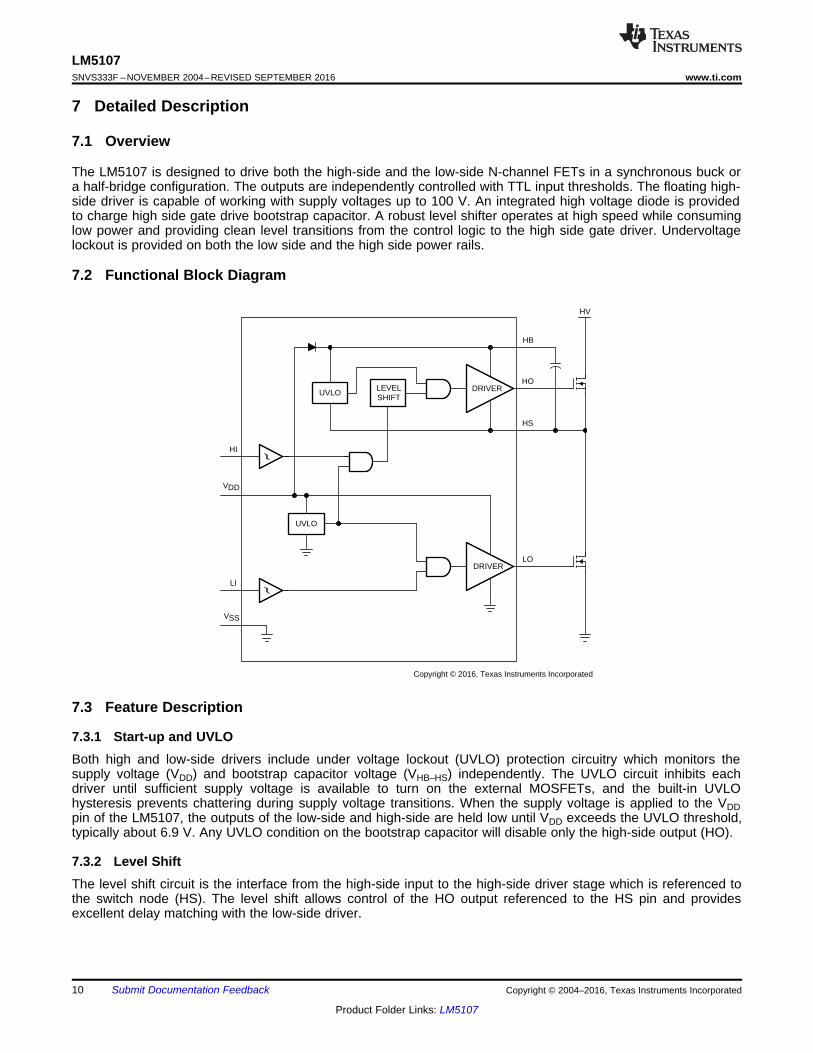
The LM5107 is designed to drive both the high-side and the low-side N-channel FETs in a synchronous buck ora half-bridge configuration. The outputs are independently controlled with TTL input thresholds. The floating high-side driver is capable of working with supply voltages up to 100 V. An integrated high voltage diode is providedto charge high side gate drive bootstrap capacitor. A robust level shifter operates at high speed while consuminglow power and providing clean level transitions from the control logic to the high side gate driver. Undervoltagelockout is provided on both the low side and the high side power rails.
7.2 Functional Block Diagram
7.3 Feature Description
7.3.1 Start-up and UVLOBoth high and low-side drivers include under voltage lockout (UVLO) protection circuitry which monitors thesupply voltage (VDD) and bootstrap capacitor voltage (VHB–HS) independently. The UVLO circuit inhibits eachdriver until sufficient supply voltage is available to turn on the external MOSFETs, and the built-in UVLOhysteresis prevents chattering during supply voltage transitions. When the supply voltage is applied to the VDDpin of the LM5107, the outputs of the low-side and high-side are held low until VDD exceeds the UVLO threshold,typically about 6.9 V. Any UVLO condition on the bootstrap capacitor will disable only the high-side output (HO).
7.3.2 Level ShiftThe level shift circuit is the interface from the high-side input to the high-side driver stage which is referenced tothe switch node (HS). The level shift allows control of the HO output referenced to the HS pin and providesexcellent delay matching with the low-side driver.

11
LM5107www.ti.com SNVS333F –NOVEMBER 2004–REVISED SEPTEMBER 2016
Product Folder Links: LM5107
Submit Documentation FeedbackCopyright © 2004–2016, Texas Instruments Incorporated
Feature Description (continued)
(1) HO is measured with respect to the HS.(2) LO is measured with the respect to the VSS.
7.3.3 Bootstrap DiodeThe bootstrap diode necessary to generate the high-side bias is included in the LM5107. The diode anode isconnected to VDD and cathode connected to VHB. With the VHB capacitor connected to HB and the HS pins, theVHB capacitor charge is refreshed every switching cycle when HS transitions to ground. The boot diode providesfast recovery times, low diode resistance, and voltage rating margin to allow for efficient and reliable operation.
7.3.4 Output StagesThe output stages are the interface to the power MOSFETs in the power train. High slew rate, low resistance,and high peak current capability of both output drivers allow for efficient switching of the power MOSFETs. Thelow-side output stage is referenced from VDD to VSS and the high-side is referenced from VHB to VHS.
7.4 Device Functional ModesThe device operates in normal mode and UVLO mode. See Start-up and UVLO for more information on UVLOoperation mode. In normal mode, the output stage is dependent on the states of the HI and LI pins.
Table 1. Input/Output Logic TableHI LI HO (1) LO (2)
L L L LL H L HH L H LH H H H

HB
PWMController
VIN
T1
RGATE
CBOOT
0.1 µF
0.47 µF
VDD
VCC
OUT1
OUT2
VDD
HI
LI
VSS
HS
LO
HO
Optional external fast recovery diode
LM5107
RBOOT
12
LM5107SNVS333F –NOVEMBER 2004–REVISED SEPTEMBER 2016 www.ti.com
Product Folder Links: LM5107
Submit Documentation Feedback Copyright © 2004–2016, Texas Instruments Incorporated
8 Application and Implementation
NOTEInformation in the following applications sections is not part of the TI componentspecification, and TI does not warrant its accuracy or completeness. TI’s customers areresponsible for determining suitability of components for their purposes. Customers shouldvalidate and test their design implementation to confirm system functionality.
8.1 Application InformationTo affect fast switching of power devices and reduce associated switching power losses, a powerful gate driver isemployed between the PWM output of controllers and the gates of the power semiconductor devices. Also, gatedrivers are indispensable when it is impossible for the PWM controller to directly drive the gates of the switchingdevices. With the advent of digital power, this situation will be often encountered because the PWM signal fromthe digital controller is often a 3.3-V logic signal which cannot effectively turn on a power switch. Level shiftingcircuitry is needed to boost the 3.3-V signal to the gate-drive voltage (such as 12 V) in order to fully turn on thepower device and minimize conduction losses. Traditional buffer drive circuits based on NPN/PNP bipolartransistors in totem-pole arrangement, being emitter follower configurations, prove inadequate with digital powerbecause they lack level-shifting capability. Gate drivers effectively combine both the level-shifting and buffer-drivefunctions. Gate drivers also find other needs such as minimizing the effect of high-frequency switching noise bylocating the high-current driver physically close to the power switch, driving gate-drive transformers andcontrolling floating power-device gates, reducing power dissipation and thermal stress in controllers by movinggate charge power losses from the controller into the driver.
The LM5107 is a high voltage gate driver that is designed to drive both the high-side and low-side N-ChannelMOSFETs in a half-bridge/full bridge configuration or in a synchronous buck circuit. The floating high side driveris capable of operating with supply voltages up to 100 V. This allows for N-Channel MOSFET control in half-bridge, full-bridge, push-pull, two switch forward and active clamp topologies. The outputs are independentlycontrolled. Each channel is controlled by its respective input pins (HI and LI), allowing full and independentflexibility to control on and off state of the output.
8.2 Typical Application
Figure 16. LM5107 Driving MOSFETs in Half-Bridge Configuration

TOTALBOOT
HB
Q 43.01nCC 1 8.7 nF
V 2.3 V= = =
D
MAXTOTAL gmax HBS
SW
D 0.95Q Q I 43 nC 10 µA 43.01nC
F 100 kHz= + = + =
13
LM5107www.ti.com SNVS333F –NOVEMBER 2004–REVISED SEPTEMBER 2016
Product Folder Links: LM5107
Submit Documentation FeedbackCopyright © 2004–2016, Texas Instruments Incorporated
Typical Application (continued)8.2.1 Design RequirementsSee Table 2 for the parameter and values.
Table 2. Operating ParametersPARAMETER VALUE
Gate Driver LM5107MOSFET CSD18531Q5A
VDD 10 VQgmax 43 nC
Fsw 100 kHzDmax 95%IHBS 10 µAVDH 1.0 VVHBR 7.1 VVHBH 0.4 V
8.2.2 Detailed Design Procedure
8.2.2.1 Select Bootstrap and VDD capacitorThe bootstrap capacitor must maintain the HB pin voltage above the UVLO voltage for the HB circuit in anycircumstances during normal operation. Calculate the maximum allowable drop across the bootstrap capacitorwith Equation 1.
ΔVHB = VDD – VDH – VHBL= 10 V – 1.0 V – 6.7 V = 2.3 V
where• VDD = Supply voltage of the gate drive IC• VDH = Bootstrap diode forward voltage drop• VHBL = VHBR – VHBH = 6.7 V, HB falling threshold (1)
The quiescent current of the bootstrap circuit is 10 µA, which is negligible compared to the Qgs of the MOSFET(see Equation 2 and Equation 3).
(2)
(3)
In practice the value for the CBOOT capacitor should be greater than that calculated to allow for situations wherethe power stage may skip pulse due to load transients. It is recommended to place the bootstrap capacitor asclose to the HB and HS pins as possible.
CBOOT = 100 nF (4)
As a general rule the local VDD bypass capacitor should be 10 times greater than the value of CBOOT.CVDD = 10 × CBOOT = 1 µF (5)
The bootstrap and bias capacitors should be ceramic types with X7R dielectric. The voltage rating should betwice that of the maximum VDD to allow for loss of capacitance once the devices have a DC bias voltage acrossthem and to ensure long-term reliability of the devices.
8.2.2.2 Select External Bootstrap Diode and ResistorThe bootstrap capacitor is charged by the VDD through the internal bootstrap diode every cycle when low sideMOSFET turns on. The charging of the capacitor involves high peak currents, and therefore transient powerdissipation in the internal bootstrap diode may be significant and dependent on its forward voltage drop. Both thediode conduction losses and reverse recovery losses contribute to the total losses in the gate driver and need tobe considered in the gate driver IC power dissipation.

DD OHLOL
GATE
V V 10 V 0.25 VI 1.30 A
R 7.5
:
DD DH OLHOL
GATE
V V V 10 V 1 V 0.25 VI 1.17 A
R 7.5
:
DD OHLOH
GATE
V V 10 V 0.45 VI 1.27 A
R 7.5
:
DD DH OHHOH
GATE
V V V 10 V 1 V 0.45 VI 1.14 A
R 7.5
:
( )DD DBOOT
DBOOT pkBOOT
V V 10 V 0.6 VI 4.27 A
R 2.2
- -= = =
W
14
LM5107SNVS333F –NOVEMBER 2004–REVISED SEPTEMBER 2016 www.ti.com
Product Folder Links: LM5107
Submit Documentation Feedback Copyright © 2004–2016, Texas Instruments Incorporated
For high frequency and high capacitive loads, it may be necessary to consider using an external bootstrap diodeplaced in parallel with internal bootstrap diode to reduce power dissipation of the driver.
Bootstrap resistor RBOOT is selected to reduce the inrush current in DBOOT and limit the ramp up slew rate ofvoltage of HB-HS. It is recommended that RBOOT is between 2 Ω and 10 Ω. For this design, a current limitingresistor of 2.2 Ω is selected to limit inrush current of bootstrap diode.
(6)
8.2.2.3 Select Gate Driver ResistorResistor RGATE is sized to reduce ringing caused by parasitic inductances and capacitances and also to limit thecurrent coming out of the gate driver. For this design 7.5-Ω resistors were selected for this design. Maximum HOand LO drive current are calculated by Equation 7 through Equation 10.
(7)
(8)
(9)
where• IHOH = Maximum HO source current• ILOH = Maximum LO source current• IHOL = Maximum HO sink current• ILOH = Maximum HO sink current• VOH = High-Level output voltage drop across HB to HO or VDD to LO• VOL = Low-Level output voltage drop across HO to HS or LO to GND (10)
8.2.3 Power DissipationPower dissipation of the gate driver has two portions as shown in Equation 11.
PDISS = PDC + PSW (11)
Use Equation 12 to calculate the DC portion of the power dissipation (PDC).PDC = IQ × VDD
where• IQ is the quiescent current for the driver. (12)
The quiescent current is the current consumed by the device to bias all internal circuits such as input stage,reference voltage, logic circuits, protections, and also any current associated with switching of internal deviceswhen the driver output changes state (such as charging and discharging of parasitic capacitances, parasiticshoot-through, and so forth). The power dissipated in the gate-driver package during switching (PSW) dependson the following factors:• Gate charge required of the power device (usually a function of the drive voltage VG, which is very close to
input bias supply voltage VDD)• Switching frequency• Use of external gate resistors. When a driver device is tested with a discrete, capacitive load calculating the
power that is required from the bias supply is fairly simple. The energy that must be transferred from the biassupply to charge the capacitor is given by Equation 13.
EG = ½CLOAD × VDD2
where

15
LM5107www.ti.com SNVS333F –NOVEMBER 2004–REVISED SEPTEMBER 2016
Product Folder Links: LM5107
Submit Documentation FeedbackCopyright © 2004–2016, Texas Instruments Incorporated
• CLOAD is load capacitor• VDD is bias voltage feeding the driver (13)
There is an equal amount of energy dissipated when the capacitor is charged and when it is discharged. Thisleads to a total power loss given by Equation 14.
PG = CLOAD × VDD2 × fSW
where• fSW is the switching frequency (14)
The switching load presented by a power MOSFET is converted to an equivalent capacitance by examining thegate charge required to switch the device. This gate charge includes the effects of the input capacitance plus theadded charge needed to swing the drain voltage of the power device as it switches between the ON and OFFstates. Most manufacturers provide specifications of typical and maximum gate charge, in nC, to switch thedevice under specified conditions. Using the gate charge Qg, determine the power that must be dissipated whenswitching a capacitor which is calculated using the equation QG = CLOAD × VDD to provide Equation 15 for power.
PG = CLOAD × VDD2 × fSW = QG × VDD × fSW (15)
This power PG is dissipated in the resistive elements of the circuit when the MOSFET is being turned on and off.Half of the total power is dissipated when the load capacitor is charged during turnon, and the other half isdissipated when the load capacitor is discharged during turnoff. When no external gate resistor is employedbetween the driver and MOSFET, this power is completely dissipated inside the driver package. With the use ofexternal gate-drive resistors, the power dissipation is shared between the internal resistance of driver andexternal gate resistor.
8.2.4 Application Curves
Figure 17. LI/HI to LO/HO Turn On Propagation Delay Figure 18. LI/HI to LO/HO Turn Off Propagation Delay

16
LM5107SNVS333F –NOVEMBER 2004–REVISED SEPTEMBER 2016 www.ti.com
Product Folder Links: LM5107
Submit Documentation Feedback Copyright © 2004–2016, Texas Instruments Incorporated
9 Power Supply Recommendations
The bias supply voltage range for which the device is rated to operate is from 8 V to 14 V. The lower end of thisrange is governed by the internal under voltage-lockout (UVLO) protection feature on the VDD pin supply circuitblocks. Whenever the driver is in UVLO condition when the VDD pin voltage is below the VDDR supply startthreshold, this feature holds the output low, regardless of the status of the inputs. The upper end of this range isdriven by the 18-V absolute maximum voltage rating of the VDD pin of the device (which is a stress rating).Keeping a 4-V margin to allow for transient voltage spikes, the maximum recommended voltage for the VDD pinis 14 V.
The UVLO protection feature also involves a hysteresis function. This means that when the VDD pin bias voltagehas exceeded the threshold voltage and device begins to operate, and if the voltage drops, then the devicecontinues to deliver normal functionality unless the voltage drop exceeds the hysteresis specification VDDH.Therefore, ensuring that, while operating at or near the 8-V range, the voltage ripple on the auxiliary powersupply output is smaller than the hysteresis specification of the device is important to avoid triggering deviceshutdown.
During system shutdown, the device operation continues until the VDD pin voltage has dropped below thethreshold (VDDR – VDDH), which must be accounted for while evaluating system shutdown timing designrequirements. Likewise, at system start up, the device does not begin operation until the VDD pin voltage hasexceeded above the VDDR threshold. The quiescent current consumed by the internal circuit blocks of the deviceis supplied through the VDD pin. Keep in mind that the charge for source current pulses delivered by the LO pinis also supplied through the same VDD pin. As a result, every time a current is sourced out of the LO pin acorresponding current pulse is delivered into the device through the VDD pin. Thus ensuring that a local bypasscapacitor is provided between the VDD and GND pins and located as close as possible to the device for thepurpose of decoupling is important. A low ESR, ceramic surface mount capacitor is necessary. TI recommendsusing two capacitors between VDD and GND: a 100-nF ceramic surface-mount capacitor that can be nudgedvery close to the pins of the device and another surface-mount capacitor in the range 0.22 µF to 10 µF added inparallel. In a similar manner, the current pulses delivered by the HO pin are sourced from the HB pin. Therefore,a 0.022-µF to 1-µF local decoupling capacitor is recommended between the HB and HS pins.
17
LM5107www.ti.com SNVS333F –NOVEMBER 2004–REVISED SEPTEMBER 2016
Product Folder Links: LM5107
Submit Documentation FeedbackCopyright © 2004–2016, Texas Instruments Incorporated
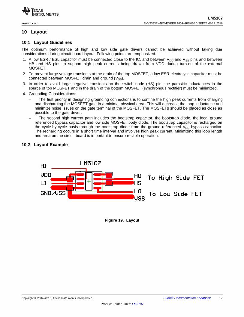
10 Layout
10.1 Layout GuidelinesThe optimum performance of high and low side gate drivers cannot be achieved without taking dueconsiderations during circuit board layout. Following points are emphasized.1. A low ESR / ESL capacitor must be connected close to the IC, and between VDD and VSS pins and between
HB and HS pins to support high peak currents being drawn from VDD during turn-on of the externalMOSFET.
2. To prevent large voltage transients at the drain of the top MOSFET, a low ESR electrolytic capacitor must beconnected between MOSFET drain and ground (VSS).
3. In order to avoid large negative transients on the switch node (HS) pin, the parasitic inductances in thesource of top MOSFET and in the drain of the bottom MOSFET (synchronous rectifier) must be minimized.
4. Grounding Considerations:– The first priority in designing grounding connections is to confine the high peak currents from charging
and discharging the MOSFET gate in a minimal physical area. This will decrease the loop inductance andminimize noise issues on the gate terminal of the MOSFET. The MOSFETs should be placed as close aspossible to the gate driver.
– The second high current path includes the bootstrap capacitor, the bootstrap diode, the local groundreferenced bypass capacitor and low side MOSFET body diode. The bootstrap capacitor is recharged onthe cycle-by-cycle basis through the bootstrap diode from the ground referenced VDD bypass capacitor.The recharging occurs in a short time interval and involves high peak current. Minimizing this loop lengthand area on the circuit board is important to ensure reliable operation.
10.2 Layout Example
Figure 19. Layout

18
LM5107SNVS333F –NOVEMBER 2004–REVISED SEPTEMBER 2016 www.ti.com
Product Folder Links: LM5107
Submit Documentation Feedback Copyright © 2004–2016, Texas Instruments Incorporated
11 Device and Documentation Support
11.1 Documentation Support
11.1.1 Related DocumentationFor additional information, see the following:
AN-1187 Leadless Leadframe Package (LLP) (SNOA401).
11.2 Receiving Notification of Documentation Updates
To receive notification of documentation updates, navigate to the device product folder on ti.com. In the upperright corner, click on Alert me to register and receive a weekly digest of any product information that haschanged. For change details, review the revision history included in any revised document.
11.3 Community ResourceThe following links connect to TI community resources. Linked contents are provided "AS IS" by the respectivecontributors. They do not constitute TI specifications and do not necessarily reflect TI's views; see TI's Terms ofUse.
TI E2E™ Online Community TI's Engineer-to-Engineer (E2E) Community. Created to foster collaborationamong engineers. At e2e.ti.com, you can ask questions, share knowledge, explore ideas and helpsolve problems with fellow engineers.
Design Support TI's Design Support Quickly find helpful E2E forums along with design support tools andcontact information for technical support.
11.4 TrademarksE2E is a trademark of Texas Instruments.All other trademarks are the property of their respective owners.
11.5 Electrostatic Discharge CautionThese devices have limited built-in ESD protection. The leads should be shorted together or the device placed in conductive foamduring storage or handling to prevent electrostatic damage to the MOS gates.
11.6 GlossarySLYZ022 — TI Glossary.
This glossary lists and explains terms, acronyms, and definitions.
12 Mechanical, Packaging, and Orderable InformationThe following pages include mechanical, packaging, and orderable information. This information is the mostcurrent data available for the designated devices. This data is subject to change without notice and revision ofthis document. For browser-based versions of this data sheet, refer to the left-hand navigation.

PACKAGE OPTION ADDENDUM
www.ti.com 30-Jul-2016
Addendum-Page 1
PACKAGING INFORMATION
Orderable Device Status(1)
Package Type PackageDrawing
Pins PackageQty
Eco Plan(2)
Lead/Ball Finish(6)
MSL Peak Temp(3)
Op Temp (°C) Device Marking(4/5)
Samples
LM5107MA/NOPB ACTIVE SOIC D 8 95 Green (RoHS& no Sb/Br)
CU SN Level-1-260C-UNLIM -40 to 125 L5107MA
LM5107MAX/NOPB ACTIVE SOIC D 8 2500 Green (RoHS& no Sb/Br)
CU SN Level-1-260C-UNLIM -40 to 125 L5107MA
LM5107SD/NOPB ACTIVE WSON NGT 8 1000 Green (RoHS& no Sb/Br)
CU SN Level-1-260C-UNLIM -40 to 125 L5107SD
(1) The marketing status values are defined as follows:ACTIVE: Product device recommended for new designs.LIFEBUY: TI has announced that the device will be discontinued, and a lifetime-buy period is in effect.NRND: Not recommended for new designs. Device is in production to support existing customers, but TI does not recommend using this part in a new design.PREVIEW: Device has been announced but is not in production. Samples may or may not be available.OBSOLETE: TI has discontinued the production of the device.
(2) Eco Plan - The planned eco-friendly classification: Pb-Free (RoHS), Pb-Free (RoHS Exempt), or Green (RoHS & no Sb/Br) - please check http://www.ti.com/productcontent for the latest availabilityinformation and additional product content details.TBD: The Pb-Free/Green conversion plan has not been defined.Pb-Free (RoHS): TI's terms "Lead-Free" or "Pb-Free" mean semiconductor products that are compatible with the current RoHS requirements for all 6 substances, including the requirement thatlead not exceed 0.1% by weight in homogeneous materials. Where designed to be soldered at high temperatures, TI Pb-Free products are suitable for use in specified lead-free processes.Pb-Free (RoHS Exempt): This component has a RoHS exemption for either 1) lead-based flip-chip solder bumps used between the die and package, or 2) lead-based die adhesive used betweenthe die and leadframe. The component is otherwise considered Pb-Free (RoHS compatible) as defined above.Green (RoHS & no Sb/Br): TI defines "Green" to mean Pb-Free (RoHS compatible), and free of Bromine (Br) and Antimony (Sb) based flame retardants (Br or Sb do not exceed 0.1% by weightin homogeneous material)
(3) MSL, Peak Temp. - The Moisture Sensitivity Level rating according to the JEDEC industry standard classifications, and peak solder temperature.
(4) There may be additional marking, which relates to the logo, the lot trace code information, or the environmental category on the device.
(5) Multiple Device Markings will be inside parentheses. Only one Device Marking contained in parentheses and separated by a "~" will appear on a device. If a line is indented then it is a continuationof the previous line and the two combined represent the entire Device Marking for that device.
(6) Lead/Ball Finish - Orderable Devices may have multiple material finish options. Finish options are separated by a vertical ruled line. Lead/Ball Finish values may wrap to two lines if the finishvalue exceeds the maximum column width.
Important Information and Disclaimer:The information provided on this page represents TI's knowledge and belief as of the date that it is provided. TI bases its knowledge and belief on informationprovided by third parties, and makes no representation or warranty as to the accuracy of such information. Efforts are underway to better integrate information from third parties. TI has taken and

PACKAGE OPTION ADDENDUM
www.ti.com 30-Jul-2016
Addendum-Page 2
continues to take reasonable steps to provide representative and accurate information but may not have conducted destructive testing or chemical analysis on incoming materials and chemicals.TI and TI suppliers consider certain information to be proprietary, and thus CAS numbers and other limited information may not be available for release.
In no event shall TI's liability arising out of such information exceed the total purchase price of the TI part(s) at issue in this document sold by TI to Customer on an annual basis.

TAPE AND REEL INFORMATION
*All dimensions are nominal
Device PackageType
PackageDrawing
Pins SPQ ReelDiameter
(mm)
ReelWidth
W1 (mm)
A0(mm)
B0(mm)
K0(mm)
P1(mm)
W(mm)
Pin1Quadrant
LM5107MAX/NOPB SOIC D 8 2500 330.0 12.4 6.5 5.4 2.0 8.0 12.0 Q1
LM5107SD/NOPB WSON NGT 8 1000 178.0 12.4 4.3 4.3 1.3 8.0 12.0 Q1
PACKAGE MATERIALS INFORMATION
www.ti.com 30-Jul-2016
Pack Materials-Page 1

*All dimensions are nominal
Device Package Type Package Drawing Pins SPQ Length (mm) Width (mm) Height (mm)
LM5107MAX/NOPB SOIC D 8 2500 367.0 367.0 35.0
LM5107SD/NOPB WSON NGT 8 1000 210.0 185.0 35.0
PACKAGE MATERIALS INFORMATION
www.ti.com 30-Jul-2016
Pack Materials-Page 2

MECHANICAL DATA
NGT0008A
www.ti.com
SDC08A (Rev A)


IMPORTANT NOTICE
Texas Instruments Incorporated and its subsidiaries (TI) reserve the right to make corrections, enhancements, improvements and otherchanges to its semiconductor products and services per JESD46, latest issue, and to discontinue any product or service per JESD48, latestissue. Buyers should obtain the latest relevant information before placing orders and should verify that such information is current andcomplete. All semiconductor products (also referred to herein as “components”) are sold subject to TI’s terms and conditions of salesupplied at the time of order acknowledgment.TI warrants performance of its components to the specifications applicable at the time of sale, in accordance with the warranty in TI’s termsand conditions of sale of semiconductor products. Testing and other quality control techniques are used to the extent TI deems necessaryto support this warranty. Except where mandated by applicable law, testing of all parameters of each component is not necessarilyperformed.TI assumes no liability for applications assistance or the design of Buyers’ products. Buyers are responsible for their products andapplications using TI components. To minimize the risks associated with Buyers’ products and applications, Buyers should provideadequate design and operating safeguards.TI does not warrant or represent that any license, either express or implied, is granted under any patent right, copyright, mask work right, orother intellectual property right relating to any combination, machine, or process in which TI components or services are used. Informationpublished by TI regarding third-party products or services does not constitute a license to use such products or services or a warranty orendorsement thereof. Use of such information may require a license from a third party under the patents or other intellectual property of thethird party, or a license from TI under the patents or other intellectual property of TI.Reproduction of significant portions of TI information in TI data books or data sheets is permissible only if reproduction is without alterationand is accompanied by all associated warranties, conditions, limitations, and notices. TI is not responsible or liable for such altereddocumentation. Information of third parties may be subject to additional restrictions.Resale of TI components or services with statements different from or beyond the parameters stated by TI for that component or servicevoids all express and any implied warranties for the associated TI component or service and is an unfair and deceptive business practice.TI is not responsible or liable for any such statements.Buyer acknowledges and agrees that it is solely responsible for compliance with all legal, regulatory and safety-related requirementsconcerning its products, and any use of TI components in its applications, notwithstanding any applications-related information or supportthat may be provided by TI. Buyer represents and agrees that it has all the necessary expertise to create and implement safeguards whichanticipate dangerous consequences of failures, monitor failures and their consequences, lessen the likelihood of failures that might causeharm and take appropriate remedial actions. Buyer will fully indemnify TI and its representatives against any damages arising out of the useof any TI components in safety-critical applications.In some cases, TI components may be promoted specifically to facilitate safety-related applications. With such components, TI’s goal is tohelp enable customers to design and create their own end-product solutions that meet applicable functional safety standards andrequirements. Nonetheless, such components are subject to these terms.No TI components are authorized for use in FDA Class III (or similar life-critical medical equipment) unless authorized officers of the partieshave executed a special agreement specifically governing such use.Only those TI components which TI has specifically designated as military grade or “enhanced plastic” are designed and intended for use inmilitary/aerospace applications or environments. Buyer acknowledges and agrees that any military or aerospace use of TI componentswhich have not been so designated is solely at the Buyer's risk, and that Buyer is solely responsible for compliance with all legal andregulatory requirements in connection with such use.TI has specifically designated certain components as meeting ISO/TS16949 requirements, mainly for automotive use. In any case of use ofnon-designated products, TI will not be responsible for any failure to meet ISO/TS16949.
Products ApplicationsAudio www.ti.com/audio Automotive and Transportation www.ti.com/automotiveAmplifiers amplifier.ti.com Communications and Telecom www.ti.com/communicationsData Converters dataconverter.ti.com Computers and Peripherals www.ti.com/computersDLP® Products www.dlp.com Consumer Electronics www.ti.com/consumer-appsDSP dsp.ti.com Energy and Lighting www.ti.com/energyClocks and Timers www.ti.com/clocks Industrial www.ti.com/industrialInterface interface.ti.com Medical www.ti.com/medicalLogic logic.ti.com Security www.ti.com/securityPower Mgmt power.ti.com Space, Avionics and Defense www.ti.com/space-avionics-defenseMicrocontrollers microcontroller.ti.com Video and Imaging www.ti.com/videoRFID www.ti-rfid.comOMAP Applications Processors www.ti.com/omap TI E2E Community e2e.ti.comWireless Connectivity www.ti.com/wirelessconnectivity
Mailing Address: Texas Instruments, Post Office Box 655303, Dallas, Texas 75265Copyright © 2016, Texas Instruments Incorporated