lmc835 digital controlled graphic equalizer - …€¦ · lmc835 digital controlled graphic...
TRANSCRIPT
TL/H/6753
LM
C835
Dig
italC
ontro
lled
Gra
phic
Equaliz
er
February 1995
LMC835 Digital Controlled Graphic Equalizer
General DescriptionThe LMC835 is a monolithic, digitally-controlled graphic
equalizer CMOS LSI for Hi-Fi audio. The LMC835 consists
of a Logic section and a Signal Path section made of analog
switches and thin-film silicon-chromium resistor networks.
The LMC835 is used with external resonator circuits to
make a stereo equalizer with seven bands, g12 dB or g6
dB gain range and 25 steps each. Only three digital inputs
are needed to control the equalization. The LMC835 makes
it easy to build a mP-controlled equalizer.
The signal path is designed for very low noise and distor-
tion, resulting in very high performance, compatible with
PCM audio.
FeaturesY No volume controls requiredY Three-wire interfaceY 14 bands, 25 steps eachY g12 dB or g6 dB gain rangesY Low noise and distortionY TTL, CMOS logic compatible
ApplicationsY Hi-Fi equalizerY ReceiverY Car stereoY Musical instrumentY Tape equalizationY MixerY Volume controller
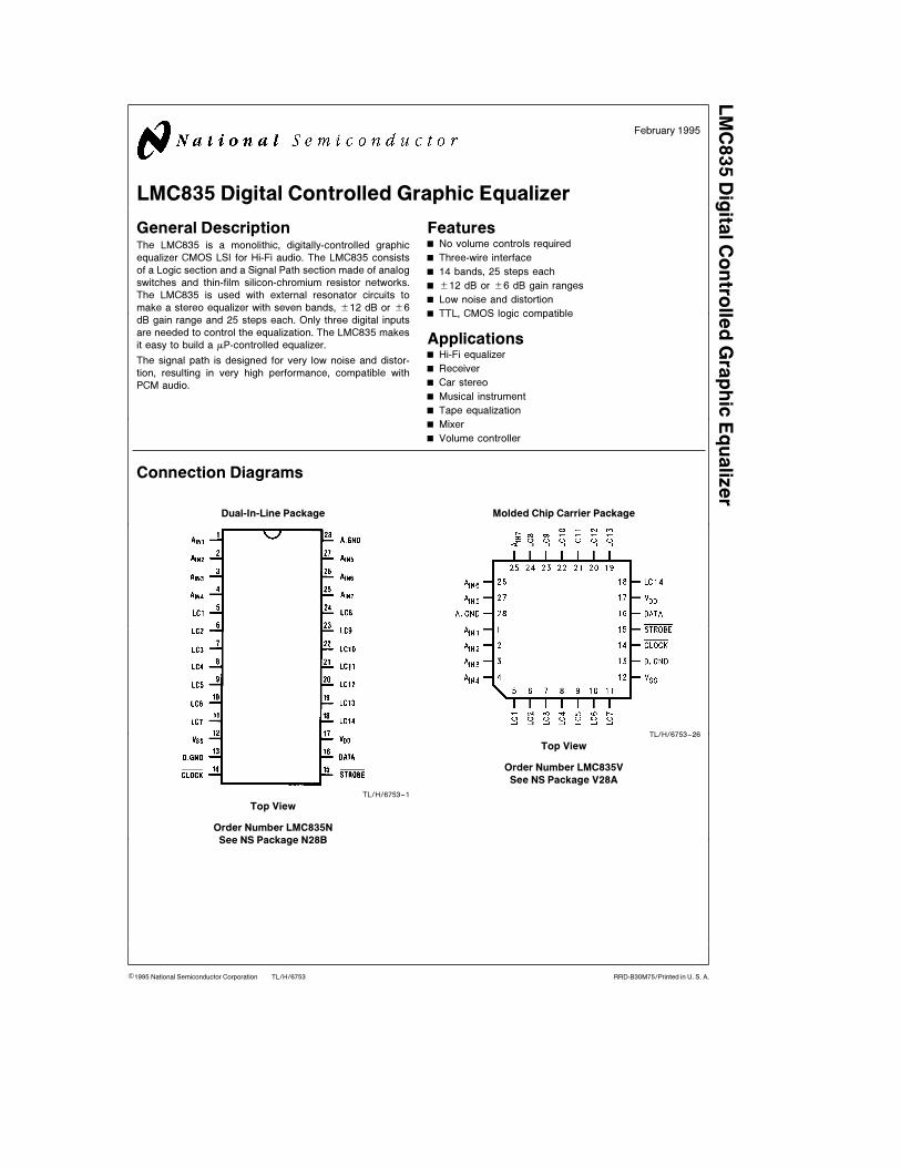
Connection Diagrams
Dual-In-Line Package
TL/H/6753–1
Top View
Order Number LMC835N
See NS Package N28B
Molded Chip Carrier Package
TL/H/6753–26
Top View
Order Number LMC835V
See NS Package V28A
C1995 National Semiconductor Corporation RRD-B30M75/Printed in U. S. A.
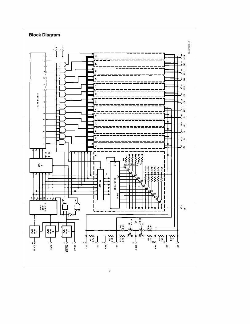
Block Diagram
TL/H
/6753–2
2

Absolute Maximum RatingsIf Military/Aerospace specified devices are required,
please contact the National Semiconductor Sales
Office/Distributors for availability and specifications.
Supply Voltage, VDDbVSS 18V
Allowable Input Voltage (Note 1) VSSb0.3V
to VDDa0.3V
Storage Temperature, Tstg b60§C to a150§CLead Temperature (Soldering, 10 sec), N Pkg a260§CLead Temperature, V Pkg
Vapor Phase (60 sec) a215§CInfrared (15 sec) a220§C
Operating RatingsSupply Voltage, VDDbVSS 5V to 16V
Digital Ground (Pin 13) VSS to VDD
Digital Input (Pins 14, 15, 16) VSS to VDD
Analog Input (Pins 1, 2, 3, 4, 25, 26, 27)
(Note 1) VSS to VDD
Operating Temperature, Topr b40§C to a85§C
Electrical Characteristics (Note 2) VDDe7.5V, VSSeb7.5V, A.GNDe0V
LOGIC SECTION
Tested DesignUnit
Symbol Parameter Test Conditions Typ Limit Limit(Limit)
(Note 3) (Note 4)
IDDL Supply Current Pins 14, 15, 16 are 0V 0.01 0.5 0.5 mA (Max)
ISSL Pins 14, 15, 16 are 0V 0.01 0.5 0.5 mA (Max)
IDDH Pins 14, 15, 16 are 5V 1.3 5 5 mA (Max)
ISSH Pins 14, 15, 16 are 5V 0.9 5 5 mA (Max)
VIH High-Level Input Voltage @Pins 14, 15, 16 1.8 2.3 2.5 V (Min)
VIL Low-Level Input Voltage @Pins 14, 15, 16 0.9 0.6 0.4 V (Max)
fo Clock Frequency @Pin 14 2000 500 500 kHz (Max)
tw(STB) Width of STB Input SeeFigure 1 0.25 1 1 ms (Min)
tsetup Data Setup Time SeeFigure 1 0.25 1 1 ms (Min)
thold Data Hold Time SeeFigure 1 0.25 1 1 ms (Min)
tcs Delay from Rising Edge of CLOCK SeeFigure 1 0.25 1 1 ms (Min)
to STB
IIN Input Current @Pins 14, 15, 16 0VkVINk5V g0.01 g1 mA (Max)
CIN Input Capacitance @Pins 14, 15, 16 fe1 MHz 5 pF
Note 1: Pins 2, 3 and 26 have a maximum input voltage range of g22V for the typical application shown in Figure 7.
Note 2: Bold numbers apply at temperature extremes. All other numbers apply at TAe25§C, VDDe7.5V, VSSeb7.5V,D.GNDeA.GNDe0V as shown in the test
circuit, Figures 3 and 4.
Note 3: Guaranteed and 100% production tested.
Note 4: Guaranteed (but not 100% production tested) over the operating temperature range. These limits are not used to calculate outgoing quality levels.
Timing Diagram
TL/H/6753–3
Note: To change the gain of the presently selected band, it is not necessary to send DATA 1 (Band Selection) each time.
FIGURE 1
3
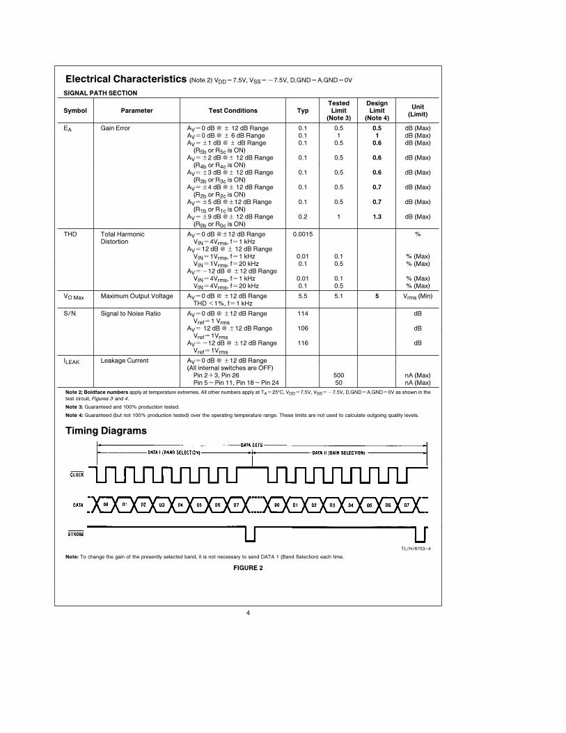
Electrical Characteristics (Note 2) VDDe7.5V, VSSeb7.5V, D.GNDeA.GNDe0V
SIGNAL PATH SECTION
Tested DesignUnit
Symbol Parameter Test Conditions Typ Limit Limit(Limit)
(Note 3) (Note 4)
EA Gain Error AVe0 dB @ g 12 dB Range 0.1 0.5 0.5 dB (Max)AVe0 dB @ g 6 dB Range 0.1 1 1 dB (Max)AVeg1 dB @ g dB Range 0.1 0.5 0.6 dB (Max)
(R5b or R5c is ON)AVeg2 dB @g 12 dB Range 0.1 0.5 0.6 dB (Max)
(R4b or R4c is ON)AVeg3 dB @g 12 dB Range 0.1 0.5 0.6 dB (Max)
(R3b or R3c is ON)AVeg4 dB @g 12 dB Range 0.1 0.5 0.7 dB (Max)
(R2b or R2c is ON)AVeg5 dB @g12 dB Range 0.1 0.5 0.7 dB (Max)
(R1b or R1c is ON)AVeg9 dB @g 12 dB Range 0.2 1 1.3 dB (Max)
(R0b or R0c is ON)
THD Total Harmonic AVe0 dB @g12 dB Range 0.0015 %Distortion VINe4Vrms, fe1 kHz
AVe12 dB @ g 12 dB RangeVINe1Vrms, fe1 kHz 0.01 0.1 % (Max)VINe1Vrms, fe20 kHz 0.1 0.5 % (Max)
AVeb12 dB @ g12 dB RangeVINe4Vrms, fe1 kHz 0.01 0.1 % (Max)VINe4Vrms, fe20 kHz 0.1 0.5 % (Max)
VO Max Maximum Output Voltage AVe0 dB @ g12 dB Range 5.5 5.1 5 Vrms (Min)THD k1%, fe1 kHz
S/N Signal to Noise Ratio AVe0 dB @ g12 dB Range 114 dBVrefe1 Vrms
AVe 12 dB @ g12 dB Range 106 dBVrefe1Vrms
AVeb12 dB @ g12 dB Range 116 dBVrefe1Vrms
ILEAK Leakage Current AVe0 dB @ g12 dB Range(All internal switches are OFF)
Pin 2a3, Pin 26 500 nA (Max)Pin 5EPin 11, Pin 18EPin 24 50 nA (Max)
Note 2; Boldface numbers apply at temperature extremes. All other numbers apply at TAe25§C, VDDe7.5V, VSSeb7.5V, D.GNDeA.GNDe0V as shown in the
test circuit, Figures 3 and 4.
Note 3: Guaranteed and 100% production tested.
Note 4: Guaranteed (but not 100% production tested) over the operating temperature range. These limits are not used to calculate outgoing quality levels.
Timing Diagrams
TL/H/6753–4
Note: To change the gain of the presently selected band, it is not necessary to send DATA 1 (Band Selection) each time.
FIGURE 2
4
Truth Tables
DATA I (Band Selection)
D7 D6 D5 D4 D3 D2 D1 D0
H X L L L L L L
H X L L L L L H
H X L L L L H L
H X L L L L H H
H X L L L H L L
H X L L L H L H
H X L L L H H L
H X L L L H H H
H X L L H L L L
H X L L H L L H
H X L L H L H L
H X L L H L H H
H X L L H H L L
H X L L H H L H
H X L L H H H L
H X L L H H H H
H X L H Valid Binary Input
H X H L Valid Binary Input
H X H H Valid Binary Input
u u u u w Band Code xj k l m
j DATA 1
k Don’t Care
l Ch A g6 dB/g12 dB Range
m Ch B g6 dB/g12 dB Range
(Ch A: Band 1E7, Ch B: Band 8E14)
Ch A g 12 dB Range, Ch B g 12 dB Range, No Band Selection
Ch A g 12 dB Range, Ch B g 12 dB Range, Band 1
Ch A g 12 dB Range, Ch B g 12 dB Range, Band 2
Ch A g 12 dB Range, Ch B g 12 dB Range, Band 3
Ch A g 12 dB Range, Ch B g 12 dB Range, Band 4
Ch A g 12 dB Range, Ch B g 12 dB Range, Band 5
Ch A g 12 dB Range, Ch B g 12 dB Range, Band 6
Ch A g 12 dB Range, Ch B g 12 dB Range, Band 7
Ch A g 12 dB Range, Ch B g 12 dB Range, Band 8
Ch A g 12 dB Range, Ch B g 12 dB Range, Band 9
Ch A g 12 dB Range, Ch B g 12 dB Range, Band 10
Ch A g 12 dB Range, Ch B g 12 dB Range, Band 11
Ch A g 12 dB Range, Ch B g 12 dB Range, Band 12
Ch A g 12 dB Range, Ch B g 12 dB Range, Band 13
Ch A g 12 dB Range, Ch B g 12 dB Range, Band 14
Ch A g 12 dB Range, Ch B g 12 dB Range, No Band Selection
Ch A g 12 dB Range, Ch B g 6 dB Range, Band 1E14
Ch A g 6 dB Range, Ch B g 12 dB Range, Band 1E14
Ch A g 6 dB Range, Ch B g 6 dB Range, Band 1E14
This is the gain if the g12 dB range is
selected by DATA I. If the g6 dB
range is selected, then the values
shown must be approximately halved.
See the characteristics curves for
more exact data.
DATA II (Gain Selection)
D7 D6 D5 D4 D3 D2 D1 D0
Flat L X L L L L L L
1 dB Boost L H H L L L L L
2 dB Boost L H L H L L L L
3 dB Boost L H L L H L L L
4 dB Boost L H L L L H L L
5 dB Boost L H L L L L H L
6 dB Boost L H L H L L H L
7 dB Boost L H H L H L H L
8 dB Boost L H L H L H H L
9 dB Boost L H L L L L L H
10 dB Boost L H H L H L L H
11 dB Boost L H H L H H L H
12 dB Boost L H H L H H H H$ 1 dBE12 dB Cut L LValid Above Input
u u w Gain Code xn o
n DATA II
o Boost/Cut
5
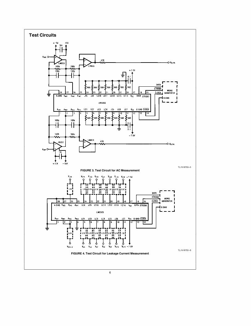
Test Circuits
TL/H/6753–5
FIGURE 3. Test Circuit for AC Measurement
TL/H/6753–6
FIGURE 4. Test Circuit for Leakage Current Measurement
6
Test Circuits (Continued)
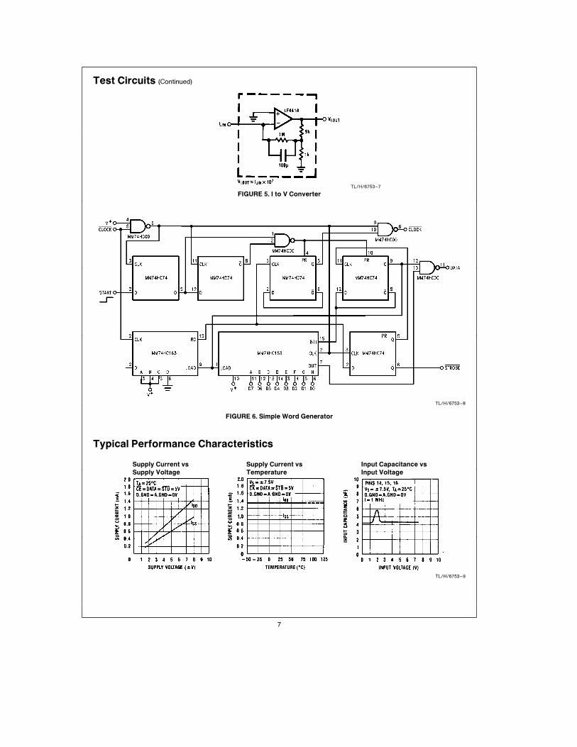
TL/H/6753–7
FIGURE 5. I to V Converter
TL/H/6753–8
FIGURE 6. Simple Word Generator
Typical Performance Characteristics
Supply Current vs
Supply Voltage
Supply Current vs
Temperature
Input Capacitance vs
Input Voltage
TL/H/6753–9
7
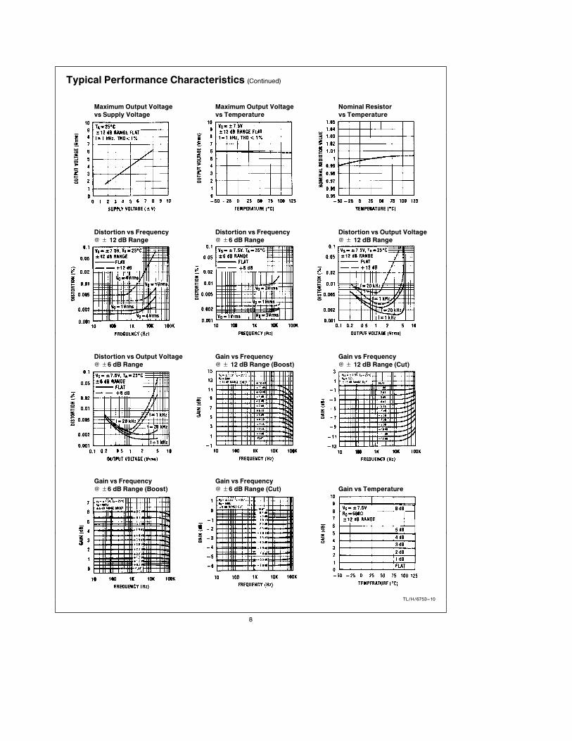
Typical Performance Characteristics (Continued)
Maximum Output Voltage
vs Supply Voltage
Maximum Output Voltage
vs Temperature
Nominal Resistor
vs Temperature
Distortion vs Frequency@ g 12 dB Range
Distortion vs Frequency@ g6 dB Range
Distortion vs Output Voltage@ g 12 dB Range
Distortion vs Output Voltage@ g6 dB Range
Gain vs Frequency@ g 12 dB Range (Boost)
Gain vs Frequency@ g 12 dB Range (Cut)
Gain vs Frequency@ g6 dB Range (Boost)
Gain vs Frequency@ g6 dB Range (Cut) Gain vs Temperature
TL/H/6753–10
8
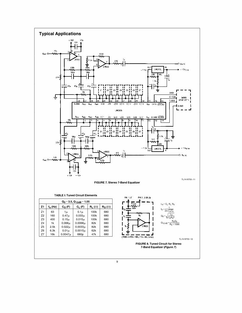
Typical Applications
TL/H/6753–11
FIGURE 7. Stereo 7-Band Equalizer
TABLE I: Tuned Circuit Elements
Q0e3.5, Q12dBe1.05
Z1 fo (Hz) CO (F) CL (F) RL (X) RO (X)
Z1 63 1m 0.1m 100k 680
Z2 160 0.47m 0.033m 100k 680
Z3 400 0.15m 0.015m 100k 680
Z4 1k 0.068m 0.0068m 82k 680
Z5 2.5k 0.022m 0.0033m 82k 680
Z6 6.3k 0.01m 0.0015m 62k 680
Z7 16k 0.0047m 680p 47k 680
TL/H/6753–12
FIGURE 8. Tuned Circuit for Stereo
7-Band Equalizer (Figure 7)
L0eCL RL R0
f0e
1
2q0L0C0
Q0e0 L0
C0R02
Q12 dBe
R0Q0
R0a1590
9
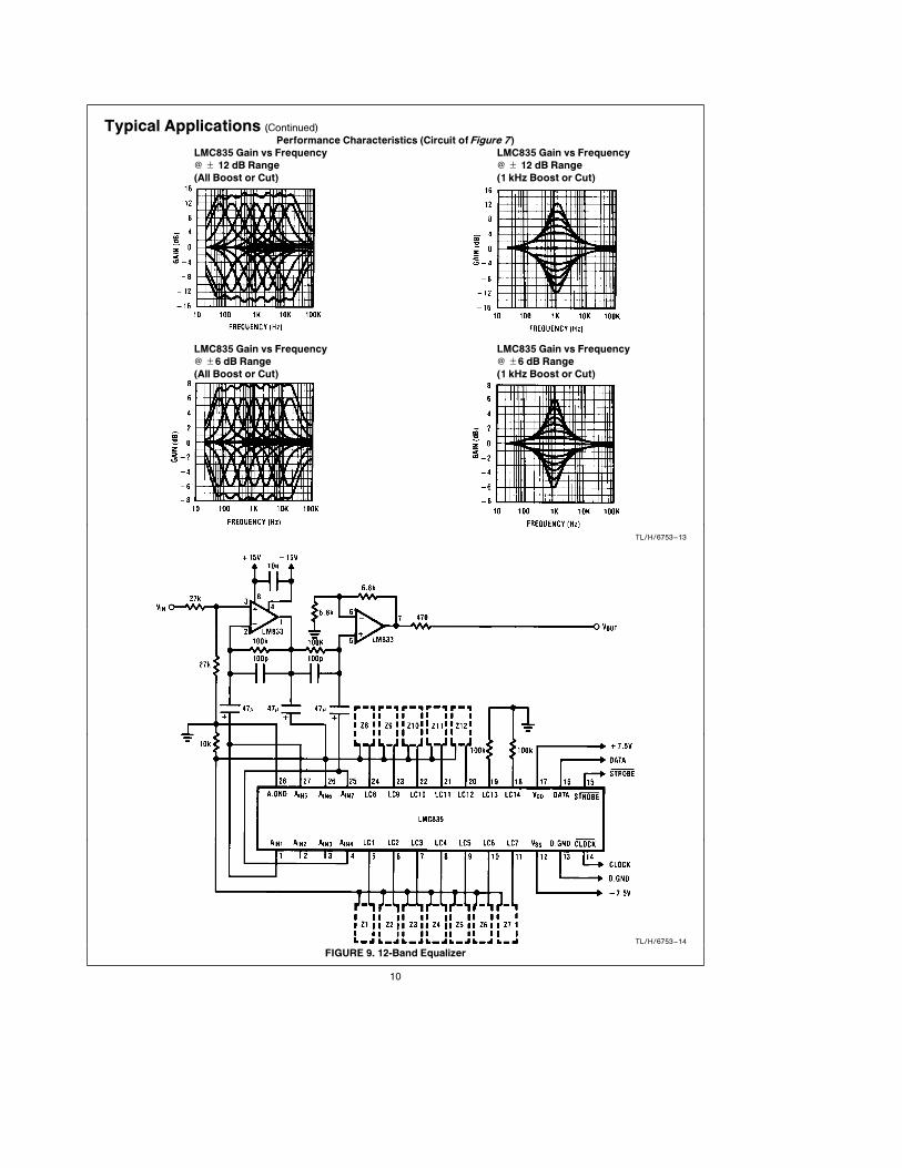
Typical Applications (Continued)
Performance Characteristics (Circuit ofFigure 7)
LMC835 Gain vs Frequency@ g 12 dB Range
(All Boost or Cut)
LMC835 Gain vs Frequency@ g 12 dB Range
(1 kHz Boost or Cut)
LMC835 Gain vs Frequency@ g6 dB Range
(All Boost or Cut)
LMC835 Gain vs Frequency@ g6 dB Range
(1 kHz Boost or Cut)
TL/H/6753–13
TL/H/6753–14
FIGURE 9. 12-Band Equalizer
10
Typical Applications (Continued)
TABLE II. Tuned Circuit Elements
Q0e4.7, Q12 dBe1.4
fo (Hz) Co (F) CL (F) RL (X) Ro (X)
Z1 16 3.3m 0.47m 100k 680
Z2 31.5 15m 0.22m 110k 680
Z3 63 1m 0.1m 100k 680
Z4 125 0.39m 0.068m 91k 680
Z5 250 0.22m 0.033m 82k 680
Z6 500 0.1m 0.015m 100k 680
Z7 1k 0.047m 0.01m 82k 680
Z8 2k 0.022m 0.0047m 91k 680
Z9 4k 0.01m 0.0022m 110k 680
Z10 8k 0.0068m 0.001m 82k 680
Z11 16k 0.0033m 680p 62k 680
Z12 32k 0.0015m 470p 68k 510
TL/H/6753–15
FIGURE 10. Tuned Circuit for
12-Band Equalizer (Figure 9)
Performance Characteristics (Circuit of Figure 9)
12 Band Equalizer Application
LMC835 Gain vs Frequency@ g6 dB Range
(All Boost or Cut)
LMC835 12 Band E.Q. Application
Gain vs Frequency@ g12 dB Range
(1 kHz Boost or Cut)
12 Band Equalizer Application
LMC835 Gain vs Frequency@ g 12 dB Range
(All Boost or Cut)
LMC835 12 Band E.Q. Application
Gain vs Frequency@ g6dB Range
(1 kHz Boost or Cut)
TL/H/6753–16
L0eCL RL R0
f0e
1
2q0L0C0
Q0e0 L0
C0R02
Q12 dBe
R0Q0
R0a1590
11
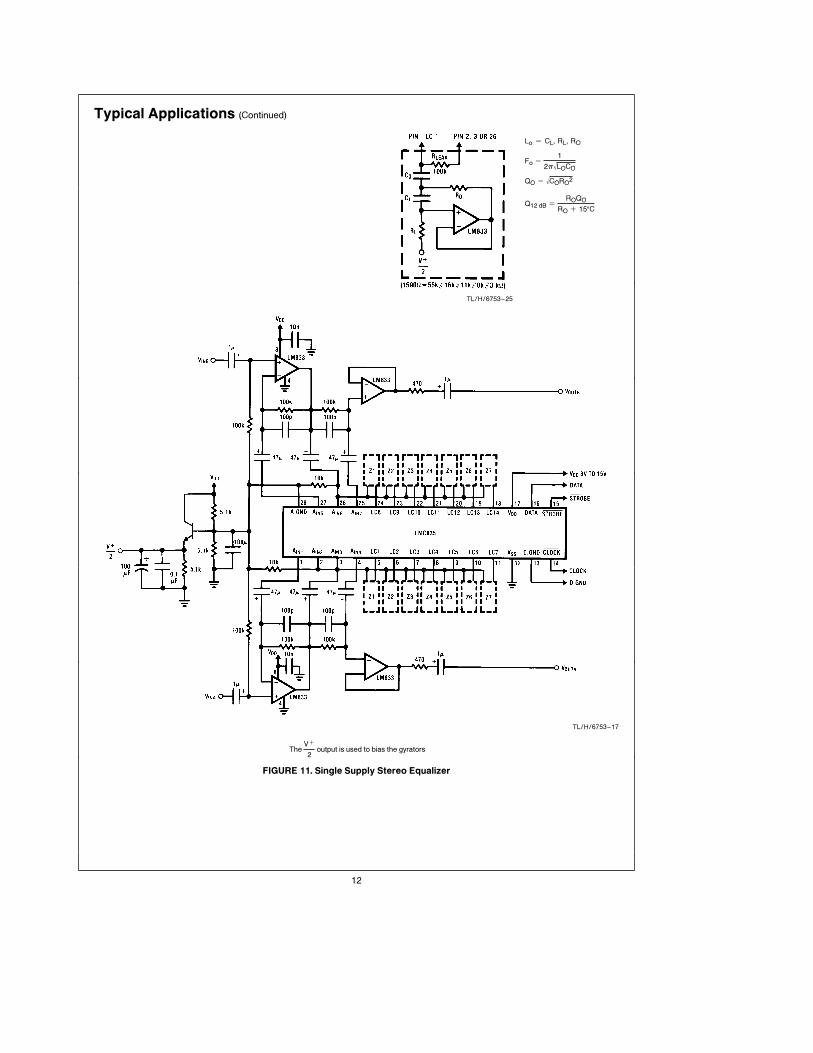
Typical Applications (Continued)
Lo e CL, RL, RO
Fo e
1
2q0LOCO
QO e 0CORO2
Q12 dB e
ROQO
RO a 15§C
TL/H/6753–25
TL/H/6753–17
TheVa
2output is used to bias the gyrators
FIGURE 11. Single Supply Stereo Equalizer
12
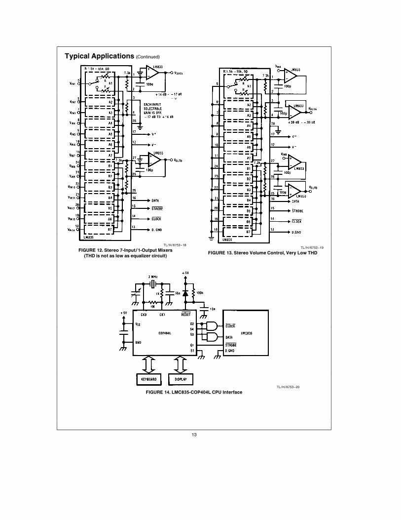
Typical Applications (Continued)
TL/H/6753–18
FIGURE 12. Stereo 7-Input/1-Output Mixers
(THD is not as low as equalizer circuit)
TL/H/6753–19
FIGURE 13. Stereo Volume Control, Very Low THD
TL/H/6753–20
FIGURE 14. LMC835-COP404L CPU Interface
13
Typical Applications (Continued)
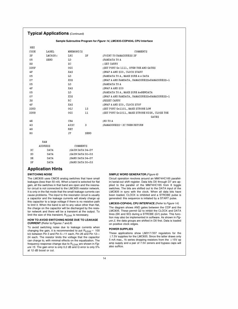
Sample Subroutine Program forFigure 14, LMC835-COP404L CPU Interface
HEX
CODE LABEL MNEMONICS COMMENTS
3F LMC835: LBI 3F ;POINT TO RAMADDRESS 3F
05 SEND LD ;RAMDATA TO A
22 SC ; SET CARRY
335F OGI ;SET PORT G4 1111, OPEN THE AND GATES
4F XAS ;SWAP A AND SIO, CLOCK START
05 LD ;RAMDATA TO A, MAKE SURE A 4 DATA
07 XDS ;SWAP A AND RAMDATA, RAMADDRESS4RAMADDRESS11
05 LD ;RAMDATA TO A
4F XAS ;SWAP A AND SIO
05 LD ;RAMDATA TO A, MAKE SURE A4NEWDATA
07 XDS ;SWAP A AND RAMDATA, RAMADDRESS4RAMADDRESS11
32 RC ;RESET CARRY
4F XAS ;SWAP A AND SIO, CLOCK STOP
335D OGJ 13 ;SET PORT G41101, MAKE STROBE LOW
335B OGI 11 ;SET PORT G41011, MAKE STROBE HIGH, CLOSE THE
GATES
4E CBA ;BD TO A
43 AISC 3 ;RAMADDRESSk3C THEN RETURN
48 RET
80 JP SEND
RAM
ADDRESS COMMENTS
3C DATA ;GAIN DATA D41D7
3D DATA ;GAIN DATA D01D3
3E DATA ;BAND DATA D41D7
3F DATA ;BAND DATA D01D3
Application HintsSWITCHING NOISE
The LMC835 uses CMOS analog switches that have small
leakages (less than 50 nA). When a band is selected for flat
gain, all the switches in that band are open and the resona-
tor circuit is not connected to the LMC835 resistor network.
It is only in the flat mode that the small leakage currents can
cause problems. The input to the resonator circuit is usually
a capacitor and the leakage currents will slowly charge up
this capacitor to a large voltage if there is no resistive path
to limit it. When the band is set to any value other than flat,
the charge on the capacitor will be discharged by the resis-
tor network and there will be a transient at the output. To
limit the size of this transient, RLEAK is necessary.
HOW TO AVOID SWITCHING NOISE DUE TO LEAKAGE
CURRENT (Refer toFigures 7 and8)
To avoid switching noise due to leakage currents when
changing the gain, it is recommended to put RLEAKe 100
kX between Pin 3 and Pin 5Ð11 each, Pin 26 and Pin 12Ð
24 each. The resistor limits the voltage that the capacitor
can charge to, with minimal effects on the equalization. The
frequency response change due to RLEAK are shown inFig-ure 15. The gain error is only 0.2 dB and Q error is only 5%
at 12 dB boost or cut.
SIMPLE WORD GENERATOR (Figure 6)
Circuit operation revolves around an MM74HC165 parallel-
in/serial-out shift register. Data bits D0 through D7 are ap-
plied to the parallel of the MM74HC165 from 8 toggle
switches. The bits are shifted out to the DATA input of the
LMC835 in sync with the clock. When all data bits have
been loaded, CLOCK is inhibited and a STROBE pulse is
generated: this sequence is initiated by a START pulse.
LMC835-COP404L CPU INTERFACE (Refer toFigure 14)
The diagram shows AND gates between the COP and the
LMC835. These permit G2 to inhibit the CLOCK and DATA
lines (SK and SO) during a STROBE (G1) pulse. This func-
tion may also be implemented in software. As shown in Fig-ure 2, the data groups are shifted in D0 first. Data is loaded
on positive clock edges.
POWER SUPPLIES
These applications show LM317/337 regulators for theg7.5V supplies for the LMC835. Since the latter draws only
5 mA max., 1k series dropping resistors from the g15V op
amp supply and a pair of 7.5V zeners and bypass caps will
also suffice.
14
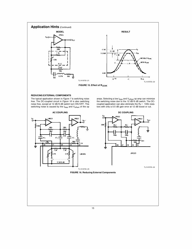
Application Hints (Continued)
MODEL
TL/H/6753–21
RESULT
TL/H/6753–22
FIGURE 15. Effect of RLEAK
REDUCING EXTERNAL COMPONENTS
The typical application shown in Figure 7 is switching noise
free. The DC-coupled circuit in Figure 16 is also switching
noise free, except at 12 dB/6 dB switch turn ON/OFF. This
switching noise is caused by the Ibias and Voffset of the op
amps. Selecting a low Ibias and Voffset op amp can minimize
the switching noise due to the 12 dB/6 dB switch. The DC-
coupled application can also eliminate the RFe 100k resis-
tors with only a 0.5 dB gain error at 12 dB boost or cut.
AC COUPLING
TL/H/6753–23
DC COUPLING
TL/H/6753–24
FIGURE 16. Reducing External Components
15

16
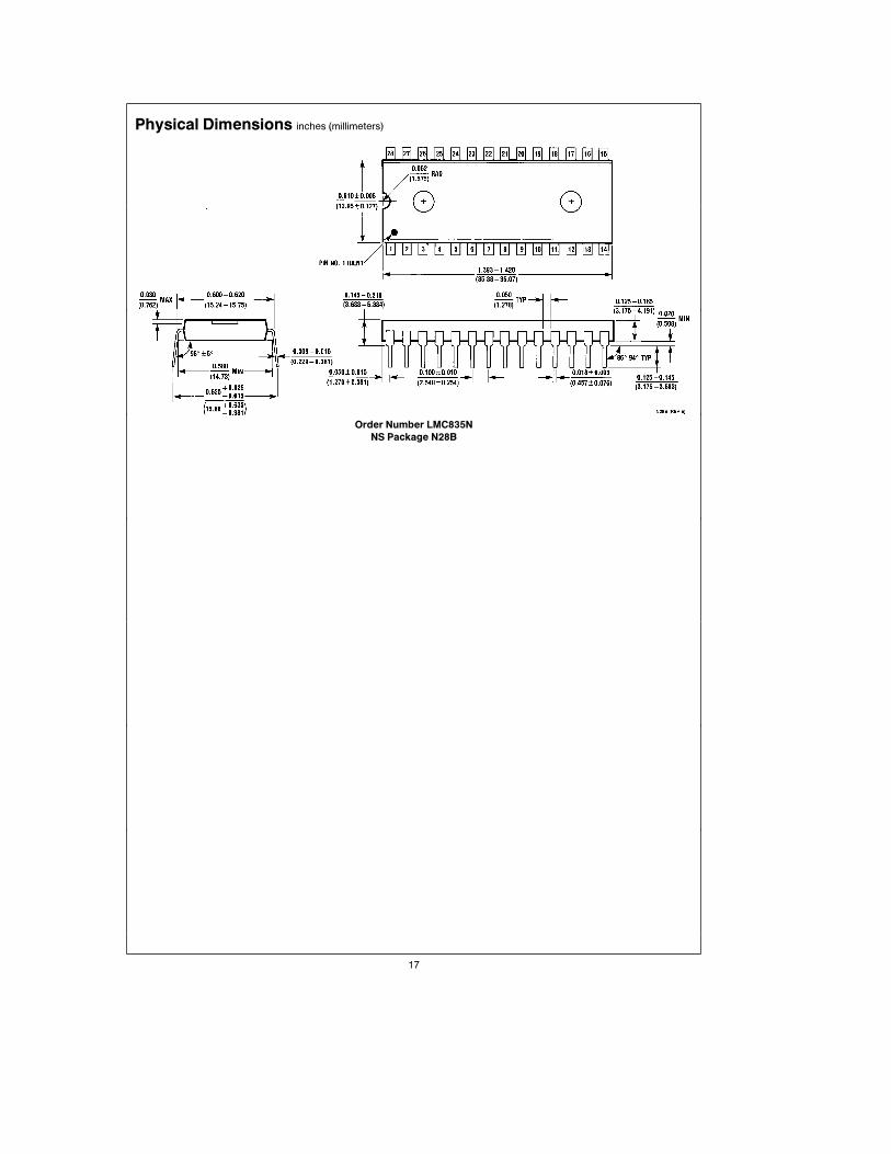
Physical Dimensions inches (millimeters)
Order Number LMC835N
NS Package N28B
17
LM
C835
Dig
italC
ontr
olled
Gra
phic
Equalizer
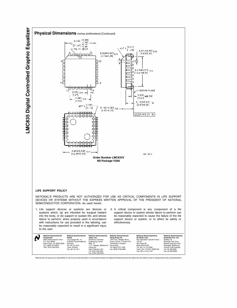
Physical Dimensions inches (millimeters) (Continued)
Order Number LMC835V
NS Package V28A
LIFE SUPPORT POLICY
NATIONAL’S PRODUCTS ARE NOT AUTHORIZED FOR USE AS CRITICAL COMPONENTS IN LIFE SUPPORT
DEVICES OR SYSTEMS WITHOUT THE EXPRESS WRITTEN APPROVAL OF THE PRESIDENT OF NATIONAL
SEMICONDUCTOR CORPORATION. As used herein:
1. Life support devices or systems are devices or 2. A critical component is any component of a life
systems which, (a) are intended for surgical implant support device or system whose failure to perform can
into the body, or (b) support or sustain life, and whose be reasonably expected to cause the failure of the life
failure to perform, when properly used in accordance support device or system, or to affect its safety or
with instructions for use provided in the labeling, can effectiveness.
be reasonably expected to result in a significant injury
to the user.
National Semiconductor National Semiconductor National Semiconductor National Semiconductor National Semiconductores National SemiconductorCorporation GmbH Japan Ltd. Hong Kong Ltd. Do Brazil Ltda. (Australia) Pty, Ltd.2900 Semiconductor Drive Livry-Gargan-Str. 10 Sumitomo Chemical 13th Floor, Straight Block, Rue Deputado Lacorda Franco Building 16P.O. Box 58090 D-82256 F 4urstenfeldbruck Engineering Center Ocean Centre, 5 Canton Rd. 120-3A Business Park DriveSanta Clara, CA 95052-8090 Germany Bldg. 7F Tsimshatsui, Kowloon Sao Paulo-SP Monash Business ParkTel: 1(800) 272-9959 Tel: (81-41) 35-0 1-7-1, Nakase, Mihama-Ku Hong Kong Brazil 05418-000 Nottinghill, MelbourneTWX: (910) 339-9240 Telex: 527649 Chiba-City, Tel: (852) 2737-1600 Tel: (55-11) 212-5066 Victoria 3168 Australia
Fax: (81-41) 35-1 Ciba Prefecture 261 Fax: (852) 2736-9960 Telex: 391-1131931 NSBR BR Tel: (3) 558-9999Tel: (043) 299-2300 Fax: (55-11) 212-1181 Fax: (3) 558-9998Fax: (043) 299-2500
National does not assume any responsibility for use of any circuitry described, no circuit patent licenses are implied and National reserves the right at any time without notice to change said circuitry and specifications.