lmh6525/lmh6526 four–channel laser diode driver with
TRANSCRIPT

LMH6525, LMH6526
www.ti.com SNOSAF1B –JUNE 2005–REVISED MARCH 2013
LMH6525/LMH6526 Four–Channel Laser Diode Driver with Dual OutputCheck for Samples: LMH6525, LMH6526
1FEATURES • LMH6525 has Differential Enable OscillatorInputs
23• Fast Switching: Rise and Fall Times: 0.6/1.0• LMH6526 has Single Ended Enable Oscillatorns.
Inputs• Low Voltage Differential Signaling (LVDS)Channels Enable Interface for the Fast
APPLICATIONSSwitching Lines• Combination DVD/CD Recordable and• Low Output Current Noise: 0.24 nA/√Hz
Rewritable Drives• Dual Output: Selectable by SELA/B Pin (Active• DVD CamcordersHIGH)• DVD Recorders– SELA = LMH6526 SEB = LMH6525
• Four Independent Current ChannelsDESCRIPTION
– Gain of 300, 300 mA Write ChannelThe LMH™6525/6526 is a laser diode driver for use
– Gain of 150, 150 mA Low-Noise Read in combination DVD/CD recordable and rewritableChannel systems. The part contains two high-current outputs
for reading and writing the DVD (650 nm) and CD– Two Gain of 150, 150 mA Write Channels(780 nm) lasers. Functionality includes read, write– 600 mA Minimum Combined Output Currentand erase through four separate switched current
• Integrated AC Coupled HFM Oscillator channels. The channel currents are summed togetherat the selected output to generate multilevel– Selectable Frequency and Amplitudewaveforms for reading, writing and erasing of opticalSettingdiscs. The LVDS interface delivers DVD write speeds– By External Resistorsof 16x and higher while minimizing noise and
– 200 MHz to 600 MHz Frequency Range crosstalk. The LMH6525/6526 is optimized for bothspeed and power consumption to meet the demands– Amplitude to 100 mA Peak-to-Peakof next generation systems. The part features a 150ModulationmA read channel plus one 300 mA and two 150 mA• Complete Shutdown by ENABLE Pin write channels, which can be summed to allow a total
• 5V Single-Supply Operation output current of 600 mA or greater. The channelcurrents are set through four independent current• Logic inputs TTL and CMOS compatibleinputs.• Space Saving Package (OFN)
1
Please be aware that an important notice concerning availability, standard warranty, and use in critical applications ofTexas Instruments semiconductor products and disclaimers thereto appears at the end of this data sheet.
2LMH is a trademark of Texas Instruments.3All other trademarks are the property of their respective owners.
PRODUCTION DATA information is current as of publication date. Copyright © 2005–2013, Texas Instruments IncorporatedProducts conform to specifications per the terms of the TexasInstruments standard warranty. Production processing does notnecessarily include testing of all parameters.
CHANNEL 3
CHANNEL 4
CHANNEL 2
READ CHANNEL
RF OSCILLATOR
OUTPUT A
OUTPUT B
I4EN4
EN4B
I3EN3
EN3B
I2EN2
EN2B
IR
ENR
ENOSC
EN
AB
LE
RF
A
RA
A
RF
B
RA
B
SE
LB
IOUTA
IOUTB
ENOSCB
VDD
VDD
VDD
VDDA
GN
DB
GN
DA
LMH6525
CHANNEL 3
CHANNEL 4
CHANNEL 2
READ CHANNEL
RF OSCILLATOR
OUTPUT A
OUTPUT B
I4EN4
EN4B
I3EN3
EN3B
I2EN2
EN2B
IR
ENR
ENOSC
IOUTA
IOUTB
VDD
VDD
VDD
VDDA
LMH6526
EN
AB
LE
RF
A
RA
A
RF
B
RA
B
SE
LA
GN
DB
GN
DA
LMH6525, LMH6526
SNOSAF1B –JUNE 2005–REVISED MARCH 2013 www.ti.com
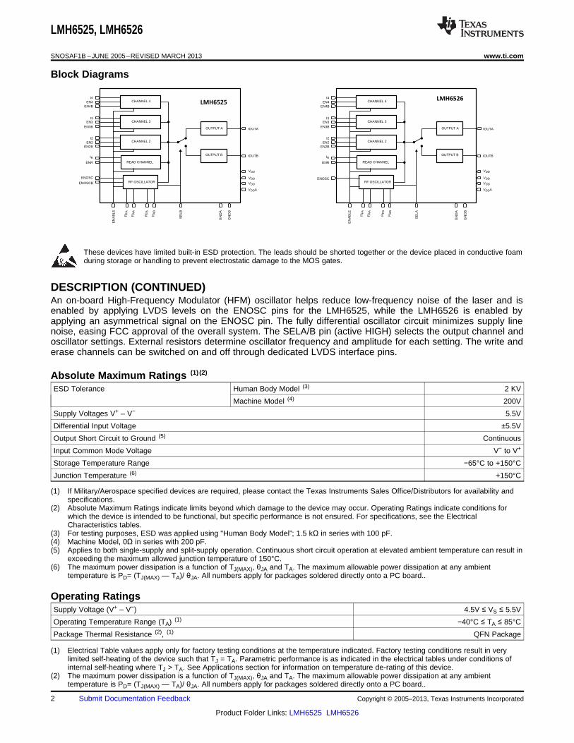
Block Diagrams
These devices have limited built-in ESD protection. The leads should be shorted together or the device placed in conductive foamduring storage or handling to prevent electrostatic damage to the MOS gates.
DESCRIPTION (CONTINUED)An on-board High-Frequency Modulator (HFM) oscillator helps reduce low-frequency noise of the laser and isenabled by applying LVDS levels on the ENOSC pins for the LMH6525, while the LMH6526 is enabled byapplying an asymmetrical signal on the ENOSC pin. The fully differential oscillator circuit minimizes supply linenoise, easing FCC approval of the overall system. The SELA/B pin (active HIGH) selects the output channel andoscillator settings. External resistors determine oscillator frequency and amplitude for each setting. The write anderase channels can be switched on and off through dedicated LVDS interface pins.
Absolute Maximum Ratings (1) (2)
ESD Tolerance Human Body Model (3) 2 KV
Machine Model (4) 200V
Supply Voltages V+ – V− 5.5V
Differential Input Voltage ±5.5V
Output Short Circuit to Ground (5) Continuous
Input Common Mode Voltage V− to V+
Storage Temperature Range −65°C to +150°C
Junction Temperature (6) +150°C
(1) If Military/Aerospace specified devices are required, please contact the Texas Instruments Sales Office/Distributors for availability andspecifications.
(2) Absolute Maximum Ratings indicate limits beyond which damage to the device may occur. Operating Ratings indicate conditions forwhich the device is intended to be functional, but specific performance is not ensured. For specifications, see the ElectricalCharacteristics tables.
(3) For testing purposes, ESD was applied using "Human Body Model”; 1.5 kΩ in series with 100 pF.(4) Machine Model, 0Ω in series with 200 pF.(5) Applies to both single-supply and split-supply operation. Continuous short circuit operation at elevated ambient temperature can result in
exceeding the maximum allowed junction temperature of 150°C.(6) The maximum power dissipation is a function of TJ(MAX), θJA and TA. The maximum allowable power dissipation at any ambient
temperature is PD= (TJ(MAX) — TA)/ θJA. All numbers apply for packages soldered directly onto a PC board..
Operating RatingsSupply Voltage (V+ – V−) 4.5V ≤ VS ≤ 5.5V
Operating Temperature Range (TA) (1) −40°C ≤ TA ≤ 85°C
Package Thermal Resistance (2), (1) QFN Package
(1) Electrical Table values apply only for factory testing conditions at the temperature indicated. Factory testing conditions result in verylimited self-heating of the device such that TJ = TA. Parametric performance is as indicated in the electrical tables under conditions ofinternal self-heating where TJ > TA. See Applications section for information on temperature de-rating of this device.
(2) The maximum power dissipation is a function of TJ(MAX), θJA and TA. The maximum allowable power dissipation at any ambienttemperature is PD= (TJ(MAX) — TA)/ θJA. All numbers apply for packages soldered directly onto a PC board..
2 Submit Documentation Feedback Copyright © 2005–2013, Texas Instruments Incorporated
Product Folder Links: LMH6525 LMH6526

LMH6525, LMH6526
www.ti.com SNOSAF1B –JUNE 2005–REVISED MARCH 2013
Operating Ratings (continued)(θJC) 3°C/W
(θJA) (no heatsink) 42°C/W
(θJA) (no heatsink see (3)) 30.8°C/W
IINR/3/4 1.5 mA (Max)
IIN2 1.0 mA (Max)
RFREQ 1000 Ω (Min)
RAMP 1000 Ω (Min)
FOSC 100-600 MHz
AOSC 10-100 mAPP
(3) This figure is taken from a thermal modeling result. The test board is a 4 layer FR-4 board measuring 101 mm x 101 mm x 1.6 mm witha 3 x 3 array of thermal vias. The ground plane on the board is 50 mm x 50 mm. Ambient temperature in simulation is 22°C, still air.Power dissipation is 1W.
Copyright © 2005–2013, Texas Instruments Incorporated Submit Documentation Feedback 3
Product Folder Links: LMH6525 LMH6526
LMH6525, LMH6526
SNOSAF1B –JUNE 2005–REVISED MARCH 2013 www.ti.com
+5V DC Electrical Characteristics (1)
Unless otherwise specified, all limits specified for TJ = 25°C, RL = 10Ω. Boldface limits apply at the temperature extremes.
Symbol Parameter Conditions Min (2) Typ (3) Max (2) Units
LVDS
VI Input Voltage Range |VGPD| < 50 mV (4) 0 1.7 2.4 V
VIDTH Input Diff. Threshold |VGPD| < 50 mV (4) –100 0 100 mV
VHYST Input Diff. Hysteresis VIDTHH – VIDTHL 25 0 mV
RIN Input Diff. Impedance 95 115 135 ΩIIN Input Current Excluding RIN Current , VCM = 1.25V 8 20 μA
Current Channels
RIN Input Resistance all Channels RIN to Ground 475 580 675 ΩIOS2 Current Offset Channel 2 Channel R,3,4 Off 2.1 16 mA
IIN = 0, EN = High
IOS,R,3,4 Current Offset Channel R,3,4 All Channels Off 1.2 9 mAIIN = 0, EN = High
AIW Current Gain Channel 2 345 386 430 A/A
AIR Current Gain Channel Read 135 159 180 A/A
AI,3,4 Current Gain Channel 3 and 4 160 182 200 A/A
ILIN-R,2,3,4 Output Current Linearity 200 μA < IIN < 1000 μA; RLOAD = 5Ω 1.7 3 %Channels Read, 2,3 and 4
IOUTW Output Current Channel 2 @ 1 mA input current 285 300 mA
IOUTR Output Current Channel Read 140 162 mA@ 1 mA input current
IOUT3,4 Output Current Channel 3 and 4 160 183 mA@ 1 mA input current
IOUTTOTAL Total Output Current All Channels (5) 600 mA
VTLO TTL Low Voltage Input (H to L), ENR 1.29 0.8 VENOSC (LMH6526)
VTLO TTL Low Voltage Input (H to L) 1.40 0.8 VB-Select (LMH6525)A-Select (LMH6526)
VELO Enable Low Voltage Enable Input (H to L) 1.98 0.8 V
VTHI TTL High Voltage Input (L to H), ENR 2 1.27 VENOSC (LMH6526)
VTHI TTL High Voltage Input (L to H) 2 1.51 VB-Select (LMH6525)A-Select (LMH6526)
VEHI Enable High Voltage Enable Input (L to H) 2.8 2.13 V
ISpd Supply Current, Power Down Enable = Low 0.003 0.1 mA
ISr1 Supply Current, Read Mode, ENOSC = Low; ENOSCB = High 81.5 100 mAOscillator Disabled I2 = I3 = I4 = IR = 125 μA
ISr2 Supply Current, Read Mode, ENOSC = High; ENOSCB = Low 81.5 100 mAOscillator Enabled I2 = I3 = I4 = IR = 125 μA
RFA = 3.5 kΩISwr Supply Current, Write Mode EN2 = EN3 = EN4 = High; 180 210 mA
I2 = I3 = I4 = IR = 125 μA
IS Supply Current All Channels disable, no input current. 33 40 mASELA/B = LowRAA, RAB, RFA, RFB = ∞
(1) Electrical Table values apply only for factory testing conditions at the temperature indicated. Factory testing conditions result in verylimited self-heating of the device such that TJ = TA. Parametric performance is as indicated in the electrical tables under conditions ofinternal self-heating where TJ > TA. See Applications section for information on temperature de-rating of this device.
(2) All limits are specified by testing or statistical analysis.(3) Typical values represent the most likely parametric norm.(4) VGPD = ground potential difference voltage between driver and receiver(5) Total input current is 4 mA (all 4 channels equal) and output currents are summed together (see typical performance characteristics).
4 Submit Documentation Feedback Copyright © 2005–2013, Texas Instruments Incorporated
Product Folder Links: LMH6525 LMH6526

LMH6525, LMH6526
www.ti.com SNOSAF1B –JUNE 2005–REVISED MARCH 2013
+5V AC ELECTRICAL CHARACTERISTICSUnless otherwise specified, all limits specified for TJ = 25°C, IOUT = 40 mA DC and 40 mA pulse, RL = 50Ω. Boldface limitsapply at the temperature extremes.
Symbol Parameter Conditions Min (1) Typ (2) Max (1) Units
tr Write Rise Time IOUT = 40 mA (Read) + 40 mA 0.6 ns(10% to 90%) RLOAD = 5Ω
tf Write Fall Time IOUT = 40 mA (Read) + 40 mA 1.6 ns(90% to 10%) RLOAD = 5Ω
tr Write Rise Time IOUT = 100 mA (Read) + 100 mA 0.6 ns(10% to 90%) RLOAD = 5Ω
tf Write Fall Time IOUT = 100 mA (Read) + 100 mA 1.0 ns(90% to 10%) RLOAD = 5Ω
tr Write Rise Time IOUT = 150 mA (Read) + 150 mA 0.6 ns(10% to 90%) RLOAD = 5Ω
tf Write Fall Time IOUT = 150 mA (Read) + 150 mA 1.0 ns(90% to 10%) RLOAD = 5Ω
OS Output Current Overshoot IOUT = 40 mA (Read) + 40 mA 18 %(3)
IN0 Output Current Noise IOUT = 40 mA; RLOAD = 50Ω; 0.24 nA/√Hzf = 50 MHz; ENOSC = Low
tON IOUT ON Prod. Delay Switched on EN2 and EN2B 3.1 ns
tOFF IOUT OFF Prop. Delay Switched on EN2 and EN2B 3.3 ns
tdisr Disable Time, Read Channel Switched on ENR 3.5 as
Tenr Enable Time, Read Channel Switched on ENR 2.8 ns
tdis Disable Time (Shutdown) Enable = High to Low 37 ns
ten Enable Time (Shutdown) Enable = Low to High 4.5 µs
BWC Channel Bandwidth, −3 dB IOUT = 50 mA, All Channels 250 KHz
FOSC Oscillator Frequency RF = 3.48 kΩ 290 360 430 MHzRange 200 MHz to 600 MHz
TDO Disable Time Oscillator LMH6525 5 ns
TEO Enable Time Oscillator LMH6525 4 ns
TDO Disable Time Oscillator LMH6526 7 ns
TEO Enable Time Oscillator LMH6526 4 ns
(1) All limits are specified by testing or statistical analysis.(2) Typical values represent the most likely parametric norm.(3) This is the average between the positive and negative overshoot.
Copyright © 2005–2013, Texas Instruments Incorporated Submit Documentation Feedback 5
Product Folder Links: LMH6525 LMH6526

67
8
9
10
11
12
13
14
15 16 17 18 19 20 21
25
IOU
TA
EN
OS
C
NC
EN
R
EN
AB
LE
VD
DA
GN
DA
RA
B
SE
LA
EN
2B
EN
2
EN
3B
EN
3
EN
4B
GNDB
IOUTB
VDD
VDD
VDD
NC
EN4
I2
I3
I4
RFA
RFB
IR
RAA
3 2 145
28
27
26
24
23
22
LMH6526
67
8
9
10
11
12
13
14
15 16 17 18 19 20 21
25IO
UT
A
EN
OS
C
EN
OS
CB
EN
R
EN
AB
LE
VD
DA
GN
DA
RA
B
SE
LB
EN
2B
EN
2
EN
3B
EN
3
EN
4B
GNDB
IOUTB
VDD
VDD
VDD
NC
EN4
I2
I3
I4
RFA
RFB
IR
RAA
3 2 145
28
27
26
24
23
22
LMH6525
LMH6525, LMH6526
SNOSAF1B –JUNE 2005–REVISED MARCH 2013 www.ti.com
CONNECTION DIAGRAMS
28-Pin (QFN)Top View
28-Pin (QFN)Top View
See Package Number NJD0028A
See Package Number NJD0028A
Table 1. Pin Description
Pin # Description Remarks
1. Laser driver output channel A
2. LVDS Oscillator Enable pin Internal Oscillator activated if logical input is high
3. LVDS Oscillator Enable pin B (only LMH6525) Internal Oscillator activated if logical input is low
4. Read Channel Enable pin Read Channel active if pin is high
5. Chip Enable pin Chip Enabled if pin is high
6. Supply Voltage A
7. Ground Connection A
8. Read Channel current setting 1 mA input current result in 150 mA output current
9. Channel 2 current setting 1 mA input current result in 300 mA output current
10. Channel 3 current setting 1 mA input current result in 150 mA output current
11. Channel 4 current setting 1 mA input current result in 150 mA output current
12. Oscillator Frequency setting Channel A Set by external resistor to ground
13. Oscillator Frequency setting Channel B Set by external resistor to ground
14. Oscillator Amplitude setting Channel A Set by external resistor to ground
15. Oscillator Amplitude setting Channel B Set by external resistor to ground
16. Channel select B (LMH6525) Channel selected if pin is highChannel select A (LMH6526)
17. LVDS input Channel 2B Channel 2 active if logical input is low
18. LVDS input Channel 2 Channel 2 active if logical input is high
19. LVDS input Channel 3B Channel 3 active if logical input is low
20. LVDS input Channel 3 Channel 3 active if logical input is high
21. LVDS input Channel 4B Channel 4 active if logical input is low
22. LVDS input Channel 4 Channel 4 active if logical input is high
23. NC
24. Supply Voltage
25. Supply Voltage
6 Submit Documentation Feedback Copyright © 2005–2013, Texas Instruments Incorporated
Product Folder Links: LMH6525 LMH6526
ON
ON
ON
ON
ON
ON
ON
AMPLITUDE
SET BY IR
AMPLITUDE
SET BY I3
AMPLITUDE
SET BY I4
SUMMATION OF
I2, I3 and I4
AMPLITUDE
SET BY I2
EN4EN4B
EN3B
EN2B
ENABLE
IOUTA
ENR
EN2
EN3
LMH6525, LMH6526
www.ti.com SNOSAF1B –JUNE 2005–REVISED MARCH 2013
Table 1. Pin Description (continued)
Pin # Description Remarks
26. Supply Voltage
27. Laser driver output channel B
28. Ground Connection B
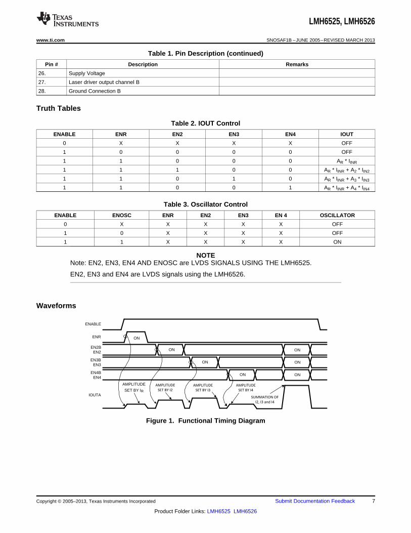
Truth Tables
Table 2. IOUT Control
ENABLE ENR EN2 EN3 EN4 IOUT
0 X X X X OFF
1 0 0 0 0 OFF
1 1 0 0 0 AR * IINR
1 1 1 0 0 AR * IINR + A2 * IIN2
1 1 0 1 0 AR * IINR + A3 * IIN3
1 1 0 0 1 AR * IINR + A4 * IIN4
Table 3. Oscillator Control
ENABLE ENOSC ENR EN2 EN3 EN 4 OSCILLATOR
0 X X X X X OFF
1 0 X X X X OFF
1 1 X X X X ON
NOTENote: EN2, EN3, EN4 AND ENOSC are LVDS SIGNALS USING THE LMH6525.
EN2, EN3 and EN4 are LVDS signals using the LMH6526.
Waveforms
Figure 1. Functional Timing Diagram
Copyright © 2005–2013, Texas Instruments Incorporated Submit Documentation Feedback 7
Product Folder Links: LMH6525 LMH6526

ENABLE
ENOSC
IOUTA
ENR
TEO TDO
EN2B,3B,4BEN2,3,4
tftr
tON tOFF
ENABLE
IOUTA
tenr
ENABLE
IOUTA
ENR
tdisr
ten
IOUTA
ENABLE
ENR
tdis
LMH6525, LMH6526
SNOSAF1B –JUNE 2005–REVISED MARCH 2013 www.ti.com
Figure 2. Enable Timing
Figure 3. Read Timing
Figure 4. Write Timing
Figure 5. Oscillator Timing
8 Submit Documentation Feedback Copyright © 2005–2013, Texas Instruments Incorporated
Product Folder Links: LMH6525 LMH6526

SHUTDOWN
CONTROL
OSC
CONTROL
ENABLE
RF
A
RF
BR
AA
RA
B
SELB (LMH6525)SELA (LMH6526)
CLOSED IF HIGH
CLOSED IF HIGH
CLOSED IF HIGH
CLOSED IF HIGH
CLOSED IF HIGH+
-
+
-
+
-
+
-
+
-
+
-
EN4
100:
EN4B
I4
500:
EN3
100:
EN3B
I3
500:
EN2
100:
EN2B
I2
500:
ENR
IR
500:
ENOSC
IOUTA
IOUTB
+
-
ENOSCB
NC at LMH6526
LMH6525, LMH6526
www.ti.com SNOSAF1B –JUNE 2005–REVISED MARCH 2013
Detailed Block Diagram
Copyright © 2005–2013, Texas Instruments Incorporated Submit Documentation Feedback 9
Product Folder Links: LMH6525 LMH6526
DAC
DAC
DAC
DAC
DIGITAL DRIVER
ENR
EN2
EN2B
EN3
EN3B
EN4
EN4B
LVDS
DRIVERS
DIGITAL LOGIC
ENOSC
ENOSCB
SELB
ENABLE
NA for LMH6526
SELA for LMH6526
DIGITAL SYSTEM
LOGIC
SELB
ENABLE
ENOSCB
ENOSC
RFA
RFB
RAA
RAB
IR
ENR
EN2
EN2B
EN3
EN3B
EN4
EN4B
OSCILLATORT
AB
GN
DA
GN
DB
NC
IOUTB
IOUTA
VD
DA
VD
D
VD
D
VD
D
LASER
DIODE
LASER
DIODE
FREQUENCY
A
FREQUENCY
B
AMPLITUDE
A
AMPLITUDE
B
LOWER RESISTANCE = HIGHER FREQUENCY AND AMPLITUDE
3k 3k 3k 3k
47 PF 68 nF 47 PF100 nF
5V 5V
BETWEEN
PINS 26
AND 28
BETWEEN
PINS 6
AND 7
6 24
25
26
8
4
9
18
17
10
20
19
11
22
21
12
13
14
15
2
3
16
5
23
27
1
GNDA AND VDDA ARE ANALOG SIGNAL GROUND AND POWER. THEY ARE NOT CONNECTED TO
GNDB AND VDD INSIDE THE CHIP
DIGITAL SYSTEM DACs
LMH6525
LMH6526
29 7
28
LMH6525, LMH6526
SNOSAF1B –JUNE 2005–REVISED MARCH 2013 www.ti.com
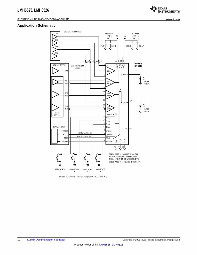
Application Schematic
10 Submit Documentation Feedback Copyright © 2005–2013, Texas Instruments Incorporated
Product Folder Links: LMH6525 LMH6526

0 1 2 3 4 5 6 7 8
0
900
OU
TP
UT
CU
RR
EN
T (
mA
)
TOTAL INPUT CURRENT (mA)
100
200
300
400
500
600
700
800
0
2.7
0.3
0.6
0.9
1.2
1.5
1.8
2.1
2.4
HE
AD
RO
OM
(V
)
VS = 5.5V
VS = 5.0V
VS = 4.5V
HEADROOM
OUTPUT CURRENT
RL = 5:
1 10 20 50
FREQUENCY (MHz)
4030
RLOAD = 25:
OSC = OFF
IDC = 40 mA
0
0.5
1
1.5
2
2.5
3
3.5
4
CU
RR
EN
T N
OIS
E (
nA/
Hz)
0 1 2 3 4 5 6 7 8 9
0
100
200
300
400
500
600
FR
EQ
UE
NC
Y (
MH
z)
RF (k:)
VS = 5V
RLOAD = 5:
0 10 20 30 40 50 60 70 80
TIME (ns)
0
0.1
0.2
0.3
0.4
0.5
OU
TP
UT
(V
)
VS = 5V
RLOAD = 5:
VSTEP = 40 mA
VDC = 40 mA
0 10 20 30 40 50 60 70 80
RA (k:)
0
20
40
60
80
100
120
140
AM
PLI
TU
DE
(m
AP
P)
VS = 5V
IDC = 150 mA
RLOAD = 10:
f = 300 MHzVS = 5V
IDC = 150 mA
RLOAD = 5:
f = 300 MHz
0 1 2 3 4 5 6 7 8 9 100
20
40
60
80
100
120
140
AM
PLI
TU
DE
(m
AP
P)
RA (k:)
VS = 5V
IDC = 150 mA
RLOAD = 10:f = 300 MHz
VS = 5V
IDC = 150 mA
RLOAD = 5:f = 300 MHz
LMH6525, LMH6526
www.ti.com SNOSAF1B –JUNE 2005–REVISED MARCH 2013
Typical Performance Characteristics(TJ = 25°C, V+ = ±5V, V− = 0V; Unless Specified).
Oscillator Amplitude Oscillator Amplitudevs. vs.RA RA
Figure 6. Figure 7.
Oscillator Frequencyvs.RF Pulse Response
Figure 8. Figure 9.
Noise Headroom & Output Currentvs. vs.
Frequency Total Input Current
Figure 10. Figure 11.
Copyright © 2005–2013, Texas Instruments Incorporated Submit Documentation Feedback 11
Product Folder Links: LMH6525 LMH6526

LMH6525, LMH6526
SNOSAF1B –JUNE 2005–REVISED MARCH 2013 www.ti.com
APPLICATION INFORMATION
CIRCUIT DESCRIPTION
General & Spec
The LMH6525/6526 is a 4-channel-input, dual-output laser driver. The dual outputs are meant to drive twodifferent laser diodes, one for CD reading and writing and one for DVD reading and writing. The part has anoscillator that can be set for both amplitude and frequency. The oscillator has four input pins for setting both theamplitude and frequency by connecting external resistors to ground. The part operates at 5V and is capable todeliver a minimum total output current of 500 mA.
INPUTS
Current-Setting Inputs
The 4 input channels are transconductance-type inputs. This means the output current of the channel isproportional to the current (not voltage) sourced into the input pin. That is why these pins are designated by theletter “I” to indicate the current input nature of the pin. The read channel current-setting pin is “IR”, the Channel 2current-setting pin is “I2” and so on. Using a transconductance-type input eliminates the high-impedance inputsassociated with a voltage input amplifier. The lower input impedances of the input nodes lowers the susceptibilityof the part to EMI/RFI. The Read Channel (IR) and Channel 3 (I3) and 4 (I4) current-setting inputs have a gain of150. The Channel 2 input (I2) has a current gain of 300. Sourcing one milliampere into the pins IR, I3 or I4, willresult in 150 mA at the output for each Channel, while 1 mA into I2 will result in 300 mA at the output for Channel2. These currents of 150 mA and 300 mA are the maximum allowable currents per channel. The total allowableoutput current from all the channels operating together exceeds 500 mA.
Channel Enable Inputs
Each of the four channels has one (read) or two enable inputs that allow the channel to be turned on or off. Theread channel enable (ENR) is a single-ended TTL/CMOS compatible input. A single-ended signal is adequate forthis channel because the read channel is generally enabled the entire time the drive is reading or writing. Thethree write/erase channels need to be operated much faster so these channel enables are LVDS (Low VoltageDifferential Signal) inputs. Each channel has two inputs, such as EN2 and EN2B. Following the standard anLVDS output consists of a current source of 3.5 mA, and this current produces across the internal terminationresistor of 100Ω in the LMH6525 or LMH6526 a voltage of 350 mV. The polarity of the current through theresistor can change very quickly thus switching the channel current on or off. The bias level of the LVDS signal isabout 1.2V, so the operating levels are 175 mV above and below this bias level. The ENxB inputs act as the notinput so if the other input is at logical ‘1’ state and the not input at ‘0’ state the channel is activated. The internal100Ω resister provides a proper termination for the LVDS signals, saving space and simplifying layout andassembly.
Control Inputs
There are two other control inputs (next to the oscillator enable which is covered in the next section). There arethe global chip Enable and output select pin SELA or SELB. Setting the Enable pin to a level above 2V willenable the part. This means the supply current raises from sleep mode value to the normal operating values. TheSELA or SELB input (TTL/ CMOS levels) controls which output is active. When at logical ‘1’ state the outputindicated by it’s name is active. The mode of this pin also controls the oscillator circuitry which means that theappropriate setting resistors become active as described in the next section.
Oscillator Inputs
The oscillator section can be switched on or off by a LVDS signal for the LMH6525 and by a TTL/ CMOS signalfor the LMH6526. When switched on the oscillator will modulate the output current. The settings of the frequencyand amplitude are done by 4 resistors, two for every channel. RFA and RFB pins set the oscillator frequency forthe A and B outputs respectively. The RAA and RAB pins set the oscillator amplitude for the A and B channelsrespectively. These 4 inputs work by having current drawn out of the pin by a setting resistor or potentiometer.The frequency and amplitude increase by decreasing setting resistor value. There are two charts in the TypicalPerformance Characteristics section that relates the setting resistor value to the resulting frequency or amplitude.Normally the settings for the frequency and amplitude are done by connecting the pin via a resistor to ground. Ifneeded to program this settings it is possible to connect these RFx and RAx pins via a current limiting resistor to
12 Submit Documentation Feedback Copyright © 2005–2013, Texas Instruments Incorporated
Product Folder Links: LMH6525 LMH6526

SUPPLY LINE
RESISTANCE
OUTPUT STAGE
LMH65xx
LASER
DIODE
SATURATED
OUTPUT
VOLTAGE
VSUPPLY
LMH6525, LMH6526
www.ti.com SNOSAF1B –JUNE 2005–REVISED MARCH 2013
the output of an op amp or DAC. When using such a circuitry the output can be held at a negative voltage, whichmeans even if the channel pins RFx and RAx are not selected, current is drawn from the pin. This is only truewhen the negative voltage has such a value that the internal transistors connected to the pin will conduct. Thiswill influence the settings of the active pins RFx and RAx. Due to this effect it is recommended, when using anegative voltage lower as -0.5V, to disable this voltage simultaneously with the channel.
OUTPUT
The outputs can source currents in excess of 600 mA. The output pins have been designed to have minimalseries inductance in order to minimize current overshoot on fast pulses. The outputs have a saturation voltage ofabout 1V. The table below shows the typical output saturation Voltages into a 5Ω load at various supply voltages.
Table 4. Output Saturation
Supply Voltage (V) Maximum Output (mA) 5Ω Saturation Voltage (V)
4.5V 700 0.8
5.0V 777 0.89
5.5V 846 1.02
As can be seen, even with a 4.5V supply voltage the part can deliver 700 mA while the saturation voltage is at0.8V. This means the output voltage of the part can be at maximum 700e-3*5 = 3.5V. With a saturated outputvoltage (see Figure 12) of 0.8V the voltage on the supply pin of the part is 4.3V. The used supply voltage is 4.5Vso there is a supply voltage loss of 0.2V over the supply line resistance, but nevertheless the part can drive laserdiodes with a forward voltage up to 3.5V with currents over 500 mA. When operating at 5.5V the part can delivercurrents over 800 mA. In this case the output at the anode of the laser diode is 846e-3*5 = 4.23V, combined withthe saturated output voltage of 1.02V the supply voltage of the part at the power pin is 5.25V and this means thesupply line loss is 0.25V. So at 5.5V supply voltage the part can drive laser diodes with a forward voltage inaccess of 4V.
Figure 12. Output Configuration
Application Hints
SUPPLY SEQUENCING
As the LMH6525/6526 is fabricated in the CMOS7 process, latch-up concerns are minimal. Be aware thatapplying a low impedance input to the part when it has no supply voltage will forward bias the ESD diode on theinput pin and then source power into the part’s VDD pin. If the potential exists for sustained operation with activeinputs and no supply voltage, all the active inputs should have series resistors to limit the current into the inputpins to levels below a few milliamperes.
Copyright © 2005–2013, Texas Instruments Incorporated Submit Documentation Feedback 13
Product Folder Links: LMH6525 LMH6526

LMH6525, LMH6526
SNOSAF1B –JUNE 2005–REVISED MARCH 2013 www.ti.com
DECOUPLING
The LMH6525/6526 has very high output currents changing within a nanosecond. This makes decouplingespecially important. High performance, low impedance ceramic capacitors should be located as close aspossible to the supply pins. The LMH6525/6526 needs two decoupling capacitors, one for the analog power andground VDDA, GNDA) and one for the power side supply and ground (3xVDD and GNDB). The high level of outputcurrent dictates the power side decoupling capacitor should be 0.1 microfarads minimum. Larger values mayimprove rise times depending on the layout and trace impedances of the connections. The capacitors shouldhave direct connection across the supply pins on the top layer, preferably with small copper-pour planes. Theseplanes can connect to the bottom side ground and/or power planes with vias but there should be a topside lowimpedance path with no vias if possible. (see also Figure 15 Decoupling Capacitors).
OVERSHOOT
As the LMH6525/6526 has fast rise times of less then a nanosecond, any inductance in the output path willcause overshoot. This includes the inductance in the laser diode itself as well as any trace inductance. A seriesconnection of a resistor and a capacitor across the laser diode could be helpful to reduce unwanted overshoot orto reduce the very high peaks caused by the relaxation oscillations of a laser diode when driven from below theknee voltage. But keep always in mind that this causes a slower rise and/ or fall time. Typical values are 10Ωand 100 pF. The actual values required depend on the laser diode used and the circuit layout and should bedetermined empirically.
THERMAL
General
The LMH6525/6526 is a very high current output device. This means that the device must have adequate heat-sinking to prevent the die from reaching its absolute maximum rating of 150°C. The primary way heat is removedfrom the LMH6525/6526 is through the Die Attach Pad, the large center pad on the bottomside of the device.Heat is also carried out of the die through the bond wires to the traces. The outputs and the VDD pads of thedevice have double bond wires on this device so they will conduct about twice as much heat to the pad. In anyevent, the heat able to be transferred out the bond wires is far less than that which can be conducted out of thedie attach pad. Heat can also be removed from the top of the part but the plastic encapsulation has worsethermal conductivity then copper. This means a heat sink on top of the part is less effective than the samecopper area on the circuit board that is thermally attached to the Die Attach Pad.
PBC Heatsinks
In order to remove the heat from the die attach pad there must be a good thermal path to large copper pours onthe circuit board. If the part is mounted on a dual-layer board the simplest method is to use 6 or 8 vias under thedie attach pad to connect the pad thermally (as well as electrically, of course) to the bottomside of the circuitboard. The vias can then conduct heat to a copper pour area with a size as large as possible. Please seeapplication note AN-1187 (Literature Number SNOA401) for guidelines about these vias and QFN packaging ingeneral.
Derating
It is essential to keep the LMH6525/6526 die under 150°C. This means that if there is inadequate heat sinkingthe part may overheat at maximum load while at maximum operating ambient of 85°C. How much power(current) the part can deliver to the load at elevated ambient temperatures is purely dependent on the amount ofheat sinking the part is provided with.
LAYOUT
Inputs
Critical inputs are the LVDS lines. These are two coupled lines of a certain impedance, mostly 100Ω. For somereason those lines could have another value but in that case the termination resistance must have the samevalue. The differential input resistance of the LMH6525 and LMH6526 is 100Ω and normally the impedance ofthe incoming transmission line matches that value. When using a flexible flat cable it is important to know theimpedance of two parallel wires in that cable. Flex cables can have different pitch distances, but a commonly
14 Submit Documentation Feedback Copyright © 2005–2013, Texas Instruments Incorporated
Product Folder Links: LMH6525 LMH6526

a
d
LMH6525, LMH6526
www.ti.com SNOSAF1B –JUNE 2005–REVISED MARCH 2013
used cable has a pitch of 0.5 mm. When verified by TDR equipment, the measurements show an impedance ofabout 142Ω. It is possible to calculate the impedance of such a cable when some parameters are known.Needed parameters are the pitch (a) of the wires, the thickness (d) en r (see Figure 13). When Checked under amicroscope: the thickness of the wires is 0.3 mm. The pitch is 0.5 mm, while the ;r must be 1 for air. Theimpedance of two parallel wires is given by this formula,
Z = (276/r) * log(2*a)/d (1)
With the data above filled in this formula the result is:Z = 144Ω (2)
Figure 13. Parallel Wires
Both the measured and the calculated numbers match very closely. The impedance of the flex cable is a physicalparameter so when designing a transmission path using this flex cable, the impedance of the total path must bebased on 140Ω. There is another parameter which is the termination resistance inside the LMH6525 or LMH6526which is 100Ω. When terminating the 140Ω transmission path with an impedance of 100Ω a mismatch will occurcausing reflections on the transmission line. To solve this problem it is possible to connect directly at the inputterminals of the part two resistors of 20Ω one on every pin to keep it symmetrical. Normally this causes signalloss over the total extra series resistance of 40Ω when using a voltage source for driving the transmission line.An advantage of a LVDS source is it’s current nature. The current of a LVDS output is 3.5 mA and this currentproduces across a resistor of 140Ω a voltage of 490 mV, while this voltage across the 100Ω internal terminationresistor of the part remains at 350 mV, which is conform the LVDS standard. With the usage of a seriesresistance of 40Ω and the termination resistor of 100Ω the total termination resistance now matches the lineimpedance and reflections will be as low as possible. A helpful tool for calculating impedances of transmissionlines is the: ‘Transmission Line Rapidesigner’ available from the Texas Instruments Interface Products Group.Application Note AN-905 (Literature Number SNLA035) details the use of this handy software tool.
The Read Enable and Enable inputs are slower and much less critical. The Oscillator Enable input is toggled incombination with the write pulse so special attention should be given to this signal to insure it is routed cleanly. Itmay be desirable to put a termination resistor close to the LMH6526 for the Enable Oscillator line, to achieve thebest turn-on and turn-off performance of the oscillator.
OUTPUTS
In order to achieve the fastest output rise times the layout of the output lines should be short and tight (seeFigure 14). It is intended that the Output B trace be routed under the decoupling capacitor and that the groundreturn for the laser be closely coupled to the output and terminated at the ground side of the decouplingcapacitor.
Copyright © 2005–2013, Texas Instruments Incorporated Submit Documentation Feedback 15
Product Folder Links: LMH6525 LMH6526

LMH6525, LMH6526
SNOSAF1B –JUNE 2005–REVISED MARCH 2013 www.ti.com
Figure 14. Laser Connection
The capacitance on the output lines should also be reduced as much as possible. As always the loop area of thelaser current should be minimized and keep in mind that it is important not to have vias in the current path of theoutput lines. Via’s will introduce some inductance which lead to extra overshoot on the pulse shape.
DECOUPLING CAPACITORS
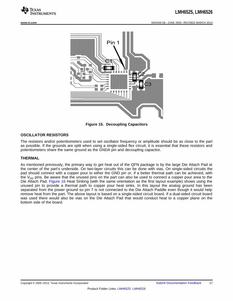
As mentioned before, the decoupling capacitors are critical to the performance of the part. The output sectionabove mentioned that the power-side decoupling capacitor should be as close as possible to the VDD and GNDpins and that the B output should pass under the decoupling capacitor. Similarly the analog-side decouplingcapacitor should be as close as possible to the VDDA and GNDA pins. Figure 15 shows a layout where theanalog (VDDA and GNDA) decoupling cap C1 is placed next to pins 6 and 7. (Note the layout is rotated 90degrees from the last figure.) The ground extends into a plane that should connect to the oscillator amplitude andcurrent setting resistors. C2 is the power-side decoupling capacitor and it can be seen placed as close to the VDDand GNDB pins as possible while straddling the B output trace. This layout has also provided for a second powerdecoupling capacitor C3 that connects from VDD to a different GND copper pour. It must be noted that the twoground planes extending from C2 and C3 must be tied together. This will be shown in the thermal section below.Bear in mind that the closeness of the parts to the LMH6525/6526 may be dictated by manufacturing reworkconsiderations such that the LMH6525/6526 can be de-soldered with a hot-air rework station without the need toremove the capacitors. The relevant manufacturing organization can provide guidelines for this minimumspacing.
16 Submit Documentation Feedback Copyright © 2005–2013, Texas Instruments Incorporated
Product Folder Links: LMH6525 LMH6526
LMH6525, LMH6526
www.ti.com SNOSAF1B –JUNE 2005–REVISED MARCH 2013
Figure 15. Decoupling Capacitors
OSCILLATOR RESISTORS
The resistors and/or potentiometers used to set oscillator frequency or amplitude should be as close to the partas possible. If the grounds are split when using a single-sided flex circuit, it is essential that these resistors andpotentiometers share the same ground as the GNDA pin and decoupling capacitor.
THERMAL
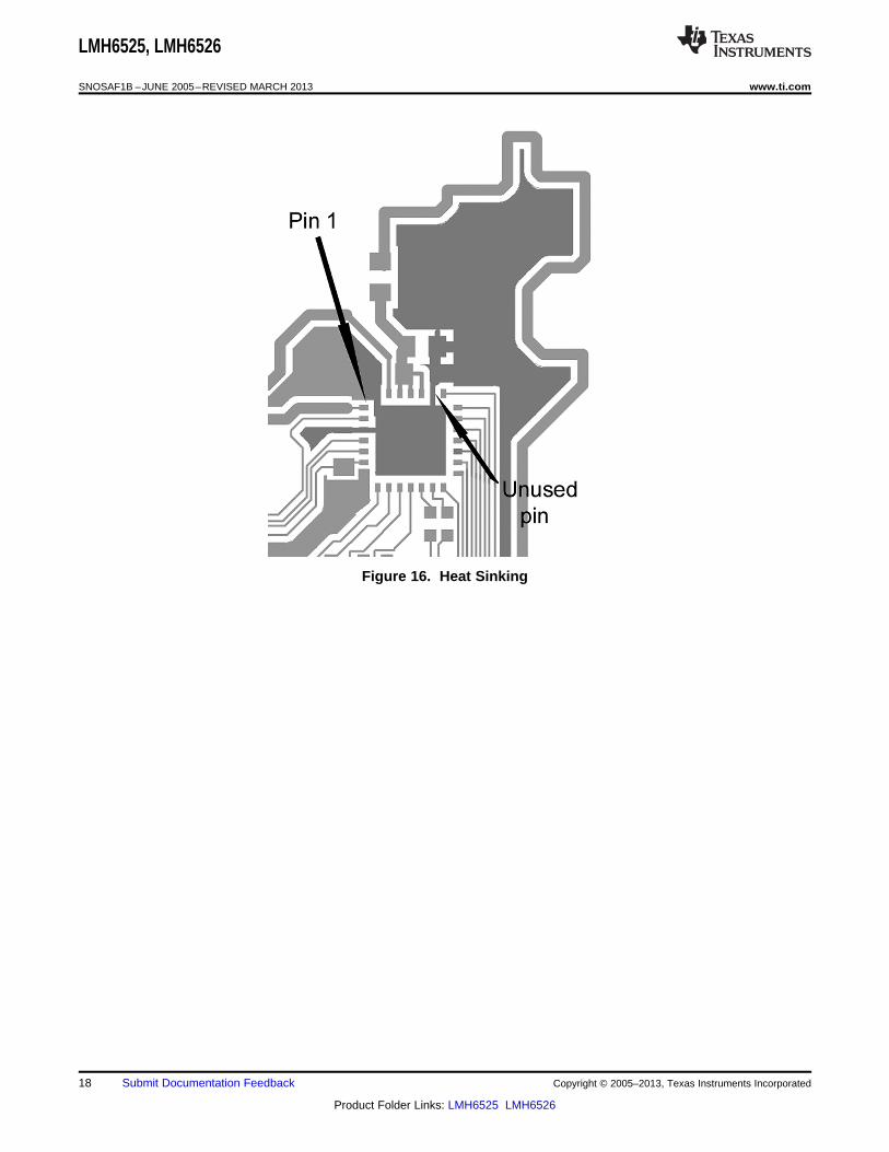
As mentioned previously, the primary way to get heat out of the QFN package is by the large Die Attach Pad atthe center of the part’s underside. On two-layer circuits this can be done with vias. On single-sided circuits thepad should connect with a copper pour to either the GND pin or, if a better thermal path can be achieved, withthe VDD pins. Be aware that the unused pins on the part can also be used to connect a copper pour area to theDie Attach Pad. Figure 16 Heat Sinking (with the same orientation as the first layout example) shows using theunused pin to provide a thermal path to copper pour heat sinks. In this layout the analog ground has beenseparated from the power ground so pin 7 is not connected to the Die Attach Paddle even though it would helpremove heat from the part. The above layout is based on a single-sided circuit board. If a dual-sided circuit boardwas used there would also be vias on the Die Attach Pad that would conduct heat to a copper plane on thebottom side of the board.
Copyright © 2005–2013, Texas Instruments Incorporated Submit Documentation Feedback 17
Product Folder Links: LMH6525 LMH6526
LMH6525, LMH6526
SNOSAF1B –JUNE 2005–REVISED MARCH 2013 www.ti.com
Figure 16. Heat Sinking
18 Submit Documentation Feedback Copyright © 2005–2013, Texas Instruments Incorporated
Product Folder Links: LMH6525 LMH6526

LMH6525, LMH6526
www.ti.com SNOSAF1B –JUNE 2005–REVISED MARCH 2013
REVISION HISTORY
Changes from Revision A (March 2013) to Revision B Page
• Changed layout of National Data Sheet to TI format .......................................................................................................... 18
Copyright © 2005–2013, Texas Instruments Incorporated Submit Documentation Feedback 19
Product Folder Links: LMH6525 LMH6526

PACKAGE OPTION ADDENDUM
www.ti.com 8-Oct-2015
Addendum-Page 1
PACKAGING INFORMATION
Orderable Device Status(1)
Package Type PackageDrawing
Pins PackageQty
Eco Plan(2)
Lead/Ball Finish(6)
MSL Peak Temp(3)
Op Temp (°C) Device Marking(4/5)
Samples
LMH6525SP/NOPB ACTIVE UQFN NJD 28 1000 Green (RoHS& no Sb/Br)
CU SN Level-1-260C-UNLIM -40 to 85 L6525SP
LMH6526SP/NOPB ACTIVE UQFN NJD 28 1000 Green (RoHS& no Sb/Br)
CU SN Level-1-260C-UNLIM -40 to 85 L6526SP
(1) The marketing status values are defined as follows:ACTIVE: Product device recommended for new designs.LIFEBUY: TI has announced that the device will be discontinued, and a lifetime-buy period is in effect.NRND: Not recommended for new designs. Device is in production to support existing customers, but TI does not recommend using this part in a new design.PREVIEW: Device has been announced but is not in production. Samples may or may not be available.OBSOLETE: TI has discontinued the production of the device.
(2) Eco Plan - The planned eco-friendly classification: Pb-Free (RoHS), Pb-Free (RoHS Exempt), or Green (RoHS & no Sb/Br) - please check http://www.ti.com/productcontent for the latest availabilityinformation and additional product content details.TBD: The Pb-Free/Green conversion plan has not been defined.Pb-Free (RoHS): TI's terms "Lead-Free" or "Pb-Free" mean semiconductor products that are compatible with the current RoHS requirements for all 6 substances, including the requirement thatlead not exceed 0.1% by weight in homogeneous materials. Where designed to be soldered at high temperatures, TI Pb-Free products are suitable for use in specified lead-free processes.Pb-Free (RoHS Exempt): This component has a RoHS exemption for either 1) lead-based flip-chip solder bumps used between the die and package, or 2) lead-based die adhesive used betweenthe die and leadframe. The component is otherwise considered Pb-Free (RoHS compatible) as defined above.Green (RoHS & no Sb/Br): TI defines "Green" to mean Pb-Free (RoHS compatible), and free of Bromine (Br) and Antimony (Sb) based flame retardants (Br or Sb do not exceed 0.1% by weightin homogeneous material)
(3) MSL, Peak Temp. - The Moisture Sensitivity Level rating according to the JEDEC industry standard classifications, and peak solder temperature.
(4) There may be additional marking, which relates to the logo, the lot trace code information, or the environmental category on the device.
(5) Multiple Device Markings will be inside parentheses. Only one Device Marking contained in parentheses and separated by a "~" will appear on a device. If a line is indented then it is a continuationof the previous line and the two combined represent the entire Device Marking for that device.
(6) Lead/Ball Finish - Orderable Devices may have multiple material finish options. Finish options are separated by a vertical ruled line. Lead/Ball Finish values may wrap to two lines if the finishvalue exceeds the maximum column width.
Important Information and Disclaimer:The information provided on this page represents TI's knowledge and belief as of the date that it is provided. TI bases its knowledge and belief on informationprovided by third parties, and makes no representation or warranty as to the accuracy of such information. Efforts are underway to better integrate information from third parties. TI has taken andcontinues to take reasonable steps to provide representative and accurate information but may not have conducted destructive testing or chemical analysis on incoming materials and chemicals.TI and TI suppliers consider certain information to be proprietary, and thus CAS numbers and other limited information may not be available for release.

PACKAGE OPTION ADDENDUM
www.ti.com 8-Oct-2015
Addendum-Page 2
In no event shall TI's liability arising out of such information exceed the total purchase price of the TI part(s) at issue in this document sold by TI to Customer on an annual basis.
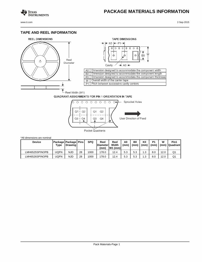
TAPE AND REEL INFORMATION
*All dimensions are nominal
Device PackageType
PackageDrawing
Pins SPQ ReelDiameter
(mm)
ReelWidth
W1 (mm)
A0(mm)
B0(mm)
K0(mm)
P1(mm)
W(mm)
Pin1Quadrant
LMH6525SP/NOPB UQFN NJD 28 1000 178.0 12.4 5.3 5.3 1.3 8.0 12.0 Q1
LMH6526SP/NOPB UQFN NJD 28 1000 178.0 12.4 5.3 5.3 1.3 8.0 12.0 Q1
PACKAGE MATERIALS INFORMATION
www.ti.com 2-Sep-2015
Pack Materials-Page 1
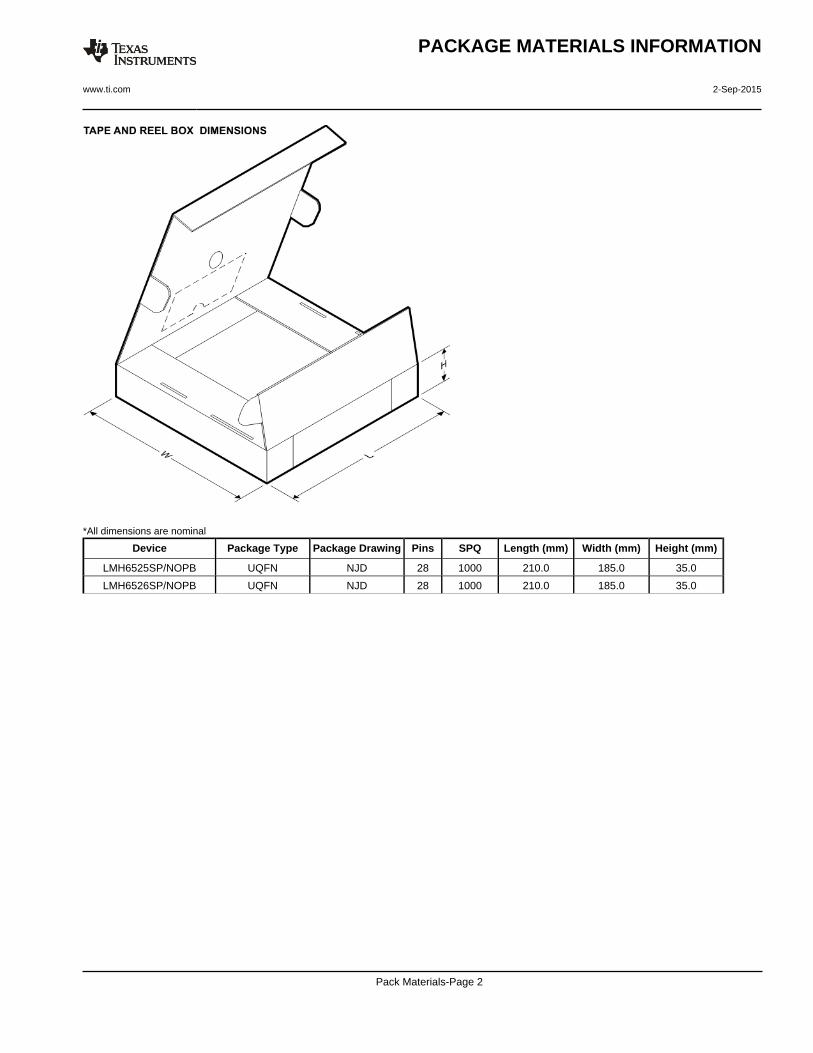
*All dimensions are nominal
Device Package Type Package Drawing Pins SPQ Length (mm) Width (mm) Height (mm)
LMH6525SP/NOPB UQFN NJD 28 1000 210.0 185.0 35.0
LMH6526SP/NOPB UQFN NJD 28 1000 210.0 185.0 35.0
PACKAGE MATERIALS INFORMATION
www.ti.com 2-Sep-2015
Pack Materials-Page 2
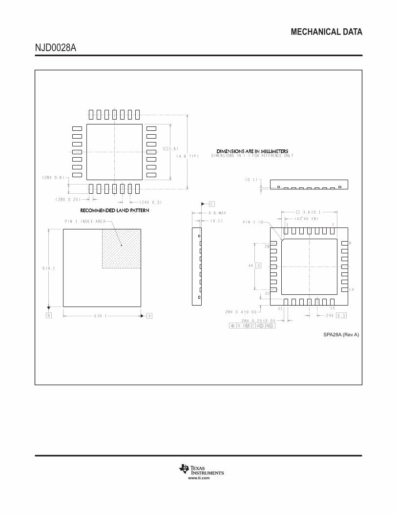
MECHANICAL DATA
NJD0028A
www.ti.com
SPA28A (Rev A)

IMPORTANT NOTICE
Texas Instruments Incorporated and its subsidiaries (TI) reserve the right to make corrections, enhancements, improvements and otherchanges to its semiconductor products and services per JESD46, latest issue, and to discontinue any product or service per JESD48, latestissue. Buyers should obtain the latest relevant information before placing orders and should verify that such information is current andcomplete. All semiconductor products (also referred to herein as “components”) are sold subject to TI’s terms and conditions of salesupplied at the time of order acknowledgment.TI warrants performance of its components to the specifications applicable at the time of sale, in accordance with the warranty in TI’s termsand conditions of sale of semiconductor products. Testing and other quality control techniques are used to the extent TI deems necessaryto support this warranty. Except where mandated by applicable law, testing of all parameters of each component is not necessarilyperformed.TI assumes no liability for applications assistance or the design of Buyers’ products. Buyers are responsible for their products andapplications using TI components. To minimize the risks associated with Buyers’ products and applications, Buyers should provideadequate design and operating safeguards.TI does not warrant or represent that any license, either express or implied, is granted under any patent right, copyright, mask work right, orother intellectual property right relating to any combination, machine, or process in which TI components or services are used. Informationpublished by TI regarding third-party products or services does not constitute a license to use such products or services or a warranty orendorsement thereof. Use of such information may require a license from a third party under the patents or other intellectual property of thethird party, or a license from TI under the patents or other intellectual property of TI.Reproduction of significant portions of TI information in TI data books or data sheets is permissible only if reproduction is without alterationand is accompanied by all associated warranties, conditions, limitations, and notices. TI is not responsible or liable for such altereddocumentation. Information of third parties may be subject to additional restrictions.Resale of TI components or services with statements different from or beyond the parameters stated by TI for that component or servicevoids all express and any implied warranties for the associated TI component or service and is an unfair and deceptive business practice.TI is not responsible or liable for any such statements.Buyer acknowledges and agrees that it is solely responsible for compliance with all legal, regulatory and safety-related requirementsconcerning its products, and any use of TI components in its applications, notwithstanding any applications-related information or supportthat may be provided by TI. Buyer represents and agrees that it has all the necessary expertise to create and implement safeguards whichanticipate dangerous consequences of failures, monitor failures and their consequences, lessen the likelihood of failures that might causeharm and take appropriate remedial actions. Buyer will fully indemnify TI and its representatives against any damages arising out of the useof any TI components in safety-critical applications.In some cases, TI components may be promoted specifically to facilitate safety-related applications. With such components, TI’s goal is tohelp enable customers to design and create their own end-product solutions that meet applicable functional safety standards andrequirements. Nonetheless, such components are subject to these terms.No TI components are authorized for use in FDA Class III (or similar life-critical medical equipment) unless authorized officers of the partieshave executed a special agreement specifically governing such use.Only those TI components which TI has specifically designated as military grade or “enhanced plastic” are designed and intended for use inmilitary/aerospace applications or environments. Buyer acknowledges and agrees that any military or aerospace use of TI componentswhich have not been so designated is solely at the Buyer's risk, and that Buyer is solely responsible for compliance with all legal andregulatory requirements in connection with such use.TI has specifically designated certain components as meeting ISO/TS16949 requirements, mainly for automotive use. In any case of use ofnon-designated products, TI will not be responsible for any failure to meet ISO/TS16949.
Products ApplicationsAudio www.ti.com/audio Automotive and Transportation www.ti.com/automotiveAmplifiers amplifier.ti.com Communications and Telecom www.ti.com/communicationsData Converters dataconverter.ti.com Computers and Peripherals www.ti.com/computersDLP® Products www.dlp.com Consumer Electronics www.ti.com/consumer-appsDSP dsp.ti.com Energy and Lighting www.ti.com/energyClocks and Timers www.ti.com/clocks Industrial www.ti.com/industrialInterface interface.ti.com Medical www.ti.com/medicalLogic logic.ti.com Security www.ti.com/securityPower Mgmt power.ti.com Space, Avionics and Defense www.ti.com/space-avionics-defenseMicrocontrollers microcontroller.ti.com Video and Imaging www.ti.com/videoRFID www.ti-rfid.comOMAP Applications Processors www.ti.com/omap TI E2E Community e2e.ti.comWireless Connectivity www.ti.com/wirelessconnectivity
Mailing Address: Texas Instruments, Post Office Box 655303, Dallas, Texas 75265Copyright © 2015, Texas Instruments Incorporated